WO2010064535A1 - 造形方法 - Google Patents
造形方法 Download PDFInfo
- Publication number
- WO2010064535A1 WO2010064535A1 PCT/JP2009/069365 JP2009069365W WO2010064535A1 WO 2010064535 A1 WO2010064535 A1 WO 2010064535A1 JP 2009069365 W JP2009069365 W JP 2009069365W WO 2010064535 A1 WO2010064535 A1 WO 2010064535A1
- Authority
- WO
- WIPO (PCT)
- Prior art keywords
- curable composition
- transfer
- group
- shape
- photocurable composition
- Prior art date
- Legal status (The legal status is an assumption and is not a legal conclusion. Google has not performed a legal analysis and makes no representation as to the accuracy of the status listed.)
- Ceased
Links
Images




Classifications
-
- B—PERFORMING OPERATIONS; TRANSPORTING
- B29—WORKING OF PLASTICS; WORKING OF SUBSTANCES IN A PLASTIC STATE IN GENERAL
- B29C—SHAPING OR JOINING OF PLASTICS; SHAPING OF MATERIAL IN A PLASTIC STATE, NOT OTHERWISE PROVIDED FOR; AFTER-TREATMENT OF THE SHAPED PRODUCTS, e.g. REPAIRING
- B29C43/00—Compression moulding, i.e. applying external pressure to flow the moulding material; Apparatus therefor
- B29C43/32—Component parts, details or accessories; Auxiliary operations
- B29C43/36—Moulds for making articles of definite length, i.e. discrete articles
-
- B—PERFORMING OPERATIONS; TRANSPORTING
- B29—WORKING OF PLASTICS; WORKING OF SUBSTANCES IN A PLASTIC STATE IN GENERAL
- B29C—SHAPING OR JOINING OF PLASTICS; SHAPING OF MATERIAL IN A PLASTIC STATE, NOT OTHERWISE PROVIDED FOR; AFTER-TREATMENT OF THE SHAPED PRODUCTS, e.g. REPAIRING
- B29C43/00—Compression moulding, i.e. applying external pressure to flow the moulding material; Apparatus therefor
- B29C43/32—Component parts, details or accessories; Auxiliary operations
- B29C43/52—Heating or cooling
-
- B—PERFORMING OPERATIONS; TRANSPORTING
- B29—WORKING OF PLASTICS; WORKING OF SUBSTANCES IN A PLASTIC STATE IN GENERAL
- B29L—INDEXING SCHEME ASSOCIATED WITH SUBCLASS B29C, RELATING TO PARTICULAR ARTICLES
- B29L2011/00—Optical elements, e.g. lenses, prisms
- B29L2011/0016—Lenses
Definitions
- the present invention relates to a modeling method for modeling a lens such as a lens array having a lens portion having an aspherical shape, or a model such as a mold used for molding such a lens.
- Patent Document 1 discloses a method of manufacturing a microlens array using a mold having a surface that forms a lens shape, and a first resin is cured on the first substrate by the mold into the lens shape.
- a method for manufacturing a microlens array including a step of forming the first substrate and a step of removing the second resin by dry etching and removing a part of the second substrate. .
- Patent Document 2 discloses a method for manufacturing a fine structure by sequentially transferring a fine pattern on a surface of a mother stamper, and (1) a step of fixing the mother stamper to a predetermined position with respect to a substrate. And (2) a step of supplying resin between the mother stamper and the substrate, (3) a step of pressing the mother stamper against the resin in a vacuum, and (4) a step of curing the resin. And (5) a step of removing the mother stamper from the cured resin, and (6) a step of moving the mother stamper or the substrate so as to change a relative position between the mother stamper and the substrate. 7) A method of manufacturing a fine structure is disclosed that includes, after the step (6), a step of repeating the steps (2) to (6) a predetermined number of times.
- Patent Document 1 and Patent Document 2 have a problem that it is difficult to mold a molded article that requires a high degree of accuracy, such as a lens having an aspherical shape.
- This invention aims at providing the modeling method which can model modeling objects, such as a lens, with high precision compared with the prior art.
- the feature of the present invention is that the object to be shaped and a transfer body on which a transfer shape having the same shape as the lens portion made of an aspheric shape or a shape opposite to the lens portion made of the aspheric shape is formed.
- a modeling method which consists of a curable composition containing the urethane compound which has a polymeric functional group, and a polymerization initiator.
- the curable composition comprises (A) silica fine particles; (B) a urethane compound represented by the following general formula (1); (Wherein R 1 is a straight chain or branched divalent aliphatic group having 1 to 12 carbon atoms, an alicyclic group having 3 to 12 carbon atoms, or an aromatic ring having carbon atoms.
- R 2 represents a linear or branched divalent aliphatic group having 1 to 10 carbon atoms, an alicyclic group having 3 to 10 carbon atoms, an aromatic ring having 6 to 30 carbon atoms.
- R 3 and R 4 are each independently a hydrogen atom or a methyl group.
- C a (meth) acrylate having an ethylenically unsaturated group and an alicyclic structure;
- D a polymerization initiator,
- R 5 represents a hydrogen atom or a methyl group
- R 6 represents an alkyl group having 1 to 3 carbon atoms or a phenyl group
- R 7 represents a hydrogen atom or a hydrocarbon group having 1 to 10 carbon atoms.
- Q is an integer from 1 to 6, and r is an integer from 0 to 2.
- the silica fine particles (A) contained in the curable composition are surface-treated with 10 to 50 parts by mass of the silane compound (E) with respect to 100 parts by mass of the silica fine particles (A). .
- the curable composition has a viscosity of 100 to 5000 mPa ⁇ s.
- the present invention it is possible to provide a modeling method capable of modeling a modeled object such as a lens with high accuracy as compared with the conventional technique.
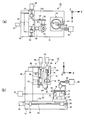
- FIG.1 (a) is a top view
- FIG.1 (b) is a left view.
- It is a 1st flowchart which shows transfer operation
- 2nd flowchart which shows operation
- the modeling apparatus 10 which concerns on the 1st Embodiment of this invention is shown.
- the modeling apparatus 10 is a modeled object and is used for modeling a lens array that is an optical component.
- the modeling apparatus 10 includes a base 12 installed on an installation surface, and a movable base 24 is supported on the base 12.
- a support base 14 is further supported on the upper surface of the movable base 24.
- the movable base 24 includes a lower part 26 in which a projecting part 25 having a shape projecting downward is formed, and an upper part 27 positioned above the lower part 26, and the projecting part 25 faces upward of the base 12. It is attached to the base 12 so as to be fitted in a groove (not shown) in the y-axis direction formed on the surface 12a. For this reason, the movable table 24 is guided by the groove in the y-axis direction, and can move in the y-axis direction on the surface 12a.
- a feed screw 28 is engaged with the protruding portion 25. The feed screw 28 is rotatably supported by the base 12 using bearings 30 and 30 so that the axial direction (longitudinal direction) is the y-axis direction.
- a y-axis motor 32 fixed to the base 12 is connected to the left end of the feed screw 28 in FIG. Therefore, by rotating the y-axis motor 32, the drive is transmitted to the projecting portion 25 via the feed screw 28, and the movable base 24 moves in the y-axis direction. Which direction of the y-axis is to be moved can be determined by controlling the rotation direction of the y-axis motor 32.
- a ⁇ -axis motor 34 is provided on the upper portion 27 of the movable table 24.
- the ⁇ -axis motor 34 rotates the upper portion 27 of the movable table 24 around a rotation axis in a direction perpendicular to the Z axis with respect to the lower portion 26 of the movable table 24.
- the movable base 24 is movable in the y-axis direction as a whole, and the upper portion 27 is rotatable with respect to the lower portion 26.
- a wafer W made of, for example, glass or the like is placed on the support base 14, and the support base 14 supports the placed wafer W from the lower side in the gravity direction.
- the support base 14 is connected to a drive source 18 including, for example, a motor.
- the support table 14 can rotate integrally with the wafer W with respect to the upper portion 27 of the movable table 24.
- spin coating It is configured as a rotary table for spin coating used in the above.
- a plurality of holes h2 for example, an injection apparatus (not shown) for injecting the curable composition as injecting is provided in the modeling apparatus 10, and the curable composition is formed in the plurality of holes h2 formed in the wafer W by the injection apparatus. You may make it inject
- the support 14 can pass light emitted from a light irradiation device 60 described later, for example, using a material having optical transparency such as glass.
- a placement / removal device (not shown) made of a robot or the like may be used. However, it may be performed manually by the operator.
- the upper portion 27 of the movable table 24 is provided with a supply device 36 for supplying a photocurable composition used as a molding object to the wafer W.
- a storage unit 40 that stores the photocurable composition is connected to the supply device 36 via a valve 38, and the supply device 36 converts the photocurable composition stored in the storage unit 40 into a substantially circular shape. It can be supplied so as to be dropped from above onto a substantially central portion of the wafer W having a (disk shape).
- the photocurable composition supplied to the wafer W is diffused by centrifugal force when the support base 14 rotates for a predetermined time, and is applied to the surface of the wafer W with a substantially uniform thickness.
- a light irradiation device 60 used as a curing device is provided on the upper portion 27 of the movable table 24.
- the light irradiation device 60 is connected to a light source 70 by an optical fiber 68 used as a light transmission means, and is used to irradiate the photocurable composition applied to the wafer W with light.
- the light irradiation device 60 is provided on the lower side, which is opposite to the transfer body 62 described later, with respect to the support base 14, the wafer W, and the photocurable composition applied to the wafer W. ing. For this reason, it is possible to irradiate the photocurable composition with light without being blocked by the transfer body 62 while the transfer body 62 is in contact with the photocurable composition.
- the movable base 24 is mounted on the base 12 and the support 42 is fixed.
- a movable unit 44 is attached to the column 42 so as to be movable in the x-axis direction with respect to the column 42.
- the movable unit 44 includes a left side portion 48 located on the left side in the drawing and a right side portion 50 fixed to the left side portion 48.
- the left portion 48 is supported so as to be movable in the x-axis direction with respect to the support column 42, and the feed screw 52 is engaged with the left portion 48.
- the feed screw 52 is rotatably attached to the column 42 by a bearing 54 so that the axis direction is the x-axis direction.
- the x-axis motor 56 attached to the column 42 is connected to one end of the feed screw 52. Therefore, when the x-axis motor 56 is rotated, the drive of the x-axis motor 56 is transmitted to the left portion 48 via the feed screw 52, and the left portion 48 and the right portion 50 of the movable unit 44 are integrated in the x-axis direction. Moving. Which direction in the x-axis direction the movable unit 44 is moved can be determined by controlling the rotation direction of the x-axis motor 56.
- a transfer body 62 is mounted on the right side portion 50 of the movable unit 44 via a support member 45.
- the support member 45 is attached to the movable unit 44 so as to be movable in the z-axis direction.
- the support member 45 includes a protrusion 46 that protrudes to the left in FIG. 1 and a support 47 that is fixed to the protrusion 46.
- the transfer body 62 is attached to the support portion 47 so that the transfer body 62 can be attached to and detached from the downward surface.
- the transfer body 62 has a shape of a lens portion to be formed and a curability used as a modeled object. Depending on the type of composition, etc., one selected from different sizes and shapes can be worn.
- a feed screw 58 is screwed into the protruding portion 46.
- the feed screw 58 is rotatably attached to the right side portion 50 of the movable unit 44 using bearings 61 and 61 so that the axial direction becomes the z-axis direction.
- the upper end of the feed screw 58 is connected to the support member z-axis motor 64. Therefore, when the support member z-axis motor 64 is rotated, the drive is transmitted to the support member 45 via the feed screw 58, and the support member 45 and the transfer body 62 supported by the support member 45 are integrated into the z-axis. Move in the direction.
- a detection device 72 used as detection means for detecting the position of the wafer W and the transfer body 62 is movable up and down independently of the support member 45 (movable in the z-axis direction). Is attached).
- the detection device 72 is, for example, a photographing unit 74 formed of a CCD camera, a lens unit 76 provided on the wafer W side of the photographing unit 74, and an illumination unit that ensures brightness for good photographing by the photographing unit 74. And a light 78 to be used.
- a z-axis motor 80 for detecting device is attached to the detecting device 72, and the z-axis motor 80 for detecting device is used as a drive source for moving the detecting device 72 in the z-axis direction with respect to the movable unit 44. Then, by moving the detection device 72 up and down, the photographing unit 74 can be focused on the transfer body 62 and the like.
- the support member 45 is attached to the movable unit 44 so as to be movable in the z-axis direction, and the movable unit 44 is attached to the support column 42 so as to be movable in the x-axis direction. Therefore, by controlling the x-axis motor 56 and the support member z-axis motor 64, the transfer member 62 can be moved in the x-axis direction and the z-axis direction together with the support member 45. Further, as described above, the support base 14 moves in the y-axis direction together with the movable base 24 and rotates by driving the y-axis motor 32 and the ⁇ -axis motor 34.
- the y-axis motor 32 controls the y-axis motor 32, the x-axis motor 56, the support member z-axis motor 64, and the ⁇ -axis motor 34, the relative positional relationship between the wafer W, the light irradiation device 60, and the transfer body 62. Can be changed.
- the photocurable composition applied to the wafer W and the transfer body 62 can be brought into contact with and separated from each other.
- the y-axis motor 32, the x-axis motor 56, the support member z-axis motor 64, and the ⁇ -axis motor 34 together with the feed screws 28, 52, 58, etc. It is used as a moving device that moves at least one of the photocurable composition and the transfer body 62 so that the transfer body 62 is brought into contact with and separated from the transfer body 62. Details of control of the y-axis motor 32, the x-axis motor 56, the support member z-axis motor 64, and the ⁇ -axis motor 34 will be described later.
- the photocurable composition is a curable composition that cures when irradiated with light.
- a photocurable composition is used as the object to be modeled.
- the transfer body 62 abuts or the transfer body 62 is pressed.
- a material that can be deformed according to the shape of the transfer body 62 and can be cured while maintaining the deformed state can be used as appropriate.
- the curable composition described above is cured by heating.
- a thermosetting composition can be used.
- the light irradiation apparatus which hardens a photocurable composition is used as a hardening apparatus which hardens a to-be-shaped object
- a hardening apparatus is suitably selected according to the material used as a to-be-shaped object. Is done. For example, when a thermosetting composition is used as the object to be modeled as described above, a heater that heats the thermosetting composition is selected as the curing device.
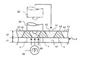
- FIG. 2 shows details of the transfer body 62 and the wafer W.
- the wafer W has a structure in which a holding plate W2 is overlaid on a substrate W1.
- the substrate W1 is made of, for example, glass that is a material that can transmit light, and the thickness t1 thereof is, for example, 400 ⁇ m.
- the holding plate W2 is made of, for example, a liquid, and is used for holding the photocurable composition before curing with high fluidity in a predetermined position, and is made of, for example, silicon, and the thickness t2 thereof is, for example, 725 ⁇ m,
- a plurality of through holes h1 penetrating from above to below are formed.
- Each through hole h1 has, for example, a mortar shape that narrows from the top to the bottom.
- the substrate W1 is in a state in which a plurality of holes h2 each having a concave shape whose bottom is sealed and opened upward are formed. Further, for example, a scribe layer (notched portion) S is formed inside the substrate W1 at a position between the adjacent through holes h1 of the substrate W1. Since the position where the scribe layer S of the substrate W1 is formed is weaker than other portions, the substrate W1 is divided along the scribe layer S when dividing the substrate W1.
- the transfer body 62 is made of, for example, metal, and has a transfer shape formed in the same shape as the lens portion 312 (see FIG. 8 to be described later) used as a lens portion having an aspheric shape or a shape opposite to the lens portion 312.
- a convex portion 90 is formed as the transfer shape.
- the transfer body 62 is used to deform the photocurable composition following the shape of the convex portion 90, and is formed on the transfer body 62 by curing the photocurable composition in the deformed state.
- the transferred shape is transferred to the photocurable composition.
- the convex portion 90 is formed by mechanically processing the transfer body 62 made of metal, for example, by using a machine tool such as a machining center, and has an aspherical shape.
- the transfer shape formed on the transfer body 62 as the convex portion 90 is required to have high accuracy, and the convex portion 90 has an aspherical shape and is difficult to process. This processing often requires a long time and high cost. Therefore, in this embodiment, in order to shorten the processing time and suppress the cost, the transfer body 62 is formed with a transfer shape only at one place.
- the aspherical shape generally refers to a surface shape other than a curved surface shape formed by cutting out a part of a spherical surface.
- the optical component such as the lens portion 312 has a shape represented by an aspherical shape expression represented by Expression (1) below.
- the photocurable composition is applied to the entire upward surface of the wafer W by spin coating, and the applied photocurable composition is applied to the holding plate W2 so as to flow into the holes h2 of the holding plate W2.
- the state in which the transfer body 62 is in contact with the photocurable composition held and held so that at least the convex portions 90 are in contact with the photocurable composition is shown.
- the photocurable composition is cured and the transfer formed on the convex portion. The shape is transferred to the photocurable composition.
- the transfer body 62 is separated from the wafer W as indicated by a two-dot chain line in FIG. 2, and is cured, for example, as indicated by an arrow in FIG. It moves so that it may contact
- an injection device (not shown) is used for the plurality of holes h ⁇ b> 2 formed in the wafer W instead of applying the photocurable composition to the entire surface of the wafer W by spin coating.
- the transfer body 62 is in contact with the photocurable composition held on the holding plate W2 so that at least the convex portions 90 are in contact with the photocurable composition.
- the state is shown. In this case, when the convex portion 90 comes into contact with the photocurable composition held in one hole h2 and light is irradiated, the photocurable composition is already in the hole h2 adjacent to the hole h2.
- the transfer body 62 is separated from the wafer W as shown by a two-dot chain line in FIG. As shown by the arrows in FIG. 5, the curable composition moves so as to be in contact with the uncured curable composition held in the hole h2 adjacent to the hole h2 holding the cured curable composition. Then, before the transfer body 62 that is in contact with the curable composition held in the adjacent hole h2 moves to the adjacent hole h2 of the adjacent hole h2, the transfer hole 62 further enters the adjacent hole h2.
- the photocurable composition is injected by an injection device.
- the photocurable composition is deformed in accordance with the transfer body 62 (deformation step).
- a photocurable composition is injected into the wafer W in which a plurality of holes h2 are formed in advance (injection step), and the photocurable composition injected into the holes h2 is brought into contact with the transfer body 62 (contact step). .
- the photocurable composition is injected into the hole h2 (injection process), and the transfer body 62 is contacted with the photocurable composition injected into the hole h2 (contact process). ) Are repeated a plurality of times.
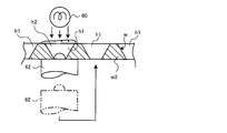
- FIG. 4 shows a first modification of the wafer W.
- the wafer W according to the above-described embodiment is configured such that the substrate W1 and the holding plate W2 are stacked.
- the substrate W1 according to the first modification includes only the holding plate W2.
- the transfer body 62 is brought into contact with the holding plate W2 from below so as to close at least one of the through holes h1 from below, and is blocked from below.
- Changing the configuration of the modeling apparatus 10 so that the photocurable composition can be supplied to the formed hole h2 from above, and the photocurable composition supplied to the hole h2 can be irradiated with light from above. Cost.
- the transfer body 62 moves so as to block the adjacent through-hole h1 from below, and thereafter The photocurable composition is injected into the adjacent hole h2 formed so as to close the through hole h1 by an injection device. Note that the same portions as those of the wafer W according to the above-described embodiment are denoted by the same reference numerals in FIG.
- the photocurable composition is held by the holding plate W2 and is held by the holding plate W2.
- the photocurable composition does not exist continuously over the entire surface of the wafer W, but is divided into a plurality of small volumes. For this reason, when the photocurable composition contracts, the shrinkage of the photocurable composition is accumulated, and an error occurs between the position where the shape of the transfer body 62 is transferred and the desired position. It is possible to prevent harmful effects. Further, the amount of the photocurable composition to be used can be reduced as compared with the case where the photocurable composition is applied to the entire surface of the substrate W1 without using the holding plate W2.
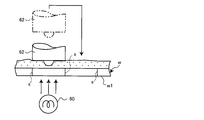
- FIG. 5 shows a second modification of the wafer W. While the wafer W according to the above-described embodiment is configured such that the substrate W1 and the holding plate W2 are stacked, in this second modification, the wafer W does not have the holding plate W2. And the substrate W1.
- the photocurable composition is applied to the entire surface of the wafer W by spin coating, and the photocurable composition applied to the wafer W is sequentially transferred. Transfer by the body 62 is performed.
- the photocurable composition is continuously present on the entire surface of the wafer W, and when the photocurable composition contracts. As the shrinkage of the photocurable composition is accumulated, an error may occur between a position where the shape of the transfer body 62 is transferred and a desired position. For this reason, in order to prevent the generation
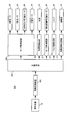
- FIG. 6 is a block diagram illustrating a control device 200 included in the modeling apparatus 10.
- the control device 200 includes a main control unit 204 to which an output from the detection device 72 is input via an image recognition device 202 that recognizes an image captured by the detection device 72.
- the main control unit 204 controls the y-axis motor 32, the x-axis motor 56, the support member z-axis motor 64, and the ⁇ -axis motor 34 by controlling the motor control circuit 206.
- the main control unit 204 controls the light source 70 by controlling the light source driving circuit 208. Further, the main control unit 204 controls the z-axis motor 80 for the detection device by controlling the motor control circuit 210.
- the main control unit 204 controls the valve 38 by controlling the valve drive circuit 212.
- the main control unit 204 controls the drive source 18 by controlling the drive source control circuit 214. Further, as described above, when the molding apparatus 10 is provided with an injection apparatus (not shown) for injecting the photocurable composition into the hole h2 formed in the wafer W, the control apparatus 200 also controls the injection apparatus. Made.
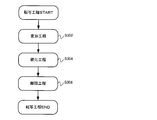
- FIG. 7 is a first flowchart showing the control of the modeling apparatus 10 by the control apparatus 200, and shows a process of a modeling method for modeling a lens array that is a modeled object and an optical component.
- the lens array refers to an optical component in which a plurality of lens portions are formed on one member.
- the first flow church shows a process in the case where the photocurable composition is applied to the entire surface of the wafer W by, for example, spin coating.
- a mounting process for mounting the wafer W on the support table 14 is executed in step S100.
- a photocurable composition application process for applying the photocurable composition to the wafer W is executed.
- the main control unit 204 controls the valve drive circuit 212 to keep the valve 38 open for a predetermined time and supply the photocurable composition to the surface of the wafer W.
- the main control unit 204 controls the drive source control circuit 214 to drive the drive source 18 for a predetermined time.
- the driving source 18 is driven, the support table 14 rotates, and the photocurable composition supplied to the wafer W placed on the support table 14 is diffused substantially uniformly on the surface of the wafer W by centrifugal force. It becomes a state.
- step S300 a transfer process for transferring the transfer shape formed on the transfer body 62 to the photocurable composition is executed. Details of the transfer process in step S300 will be described later.
- next step S400 it is determined whether or not all the transfer processes have been completed. That is, as step S300, for example, it is determined whether or not it is the last transfer process among the transfer processes repeated about 1500 to 2400 times. If it is determined in step S400 that it is not the last transfer process, the process returns to step S300. On the other hand, if it is determined in step S300 that it is the last transfer process, the process proceeds to the next step S500.
- step S500 the wafer W transferred to the applied photocurable composition is unloaded from the modeling apparatus 10 from the state of being placed on the support base 14.
- the modeling apparatus 10 does not have a device such as a robot that places the wafer W on the support table 14 and carries the wafer W out of the modeling apparatus 10
- the wafer W is placed on the support table 14.
- the removal of the wafer W from the modeling apparatus 10 is performed manually by the operator, and the operations of Step S100 and Step S500 under the control of the main control unit 204 are not performed.
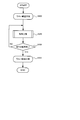
- FIG. 8 is a first flowchart showing a transfer process by the control device 200.
- the transfer body 62 is applied to the thermosetting composition.
- 5 is a flowchart showing details of control in a transfer step (step S300) for transferring a transfer shape formed in the step.
- a deforming process is performed in which the photocurable composition applied to the wafer W is deformed in accordance with the transfer shape formed on the transfer body 62 in step S302.
- step S302 the main control unit 204 controls the motor control circuit 206 to drive the y-axis motor 32, the x-axis motor 56, the support member z-axis motor 64, and the ⁇ -axis motor 34, and thereby the wafer W. At least one of the transfer body 62 and the support 14 is moved so that the predetermined position of the photocurable composition applied to the film contacts the transfer body 62 and deforms the photocurable composition.
- step S302 based on the data detected by the detection device 72 and subjected to image processing by the image recognition device 202, the support base 14 and the support base 14 and the transfer base 62 come into contact with the appropriate position of the photocurable composition.
- Position correction data may be created on the transfer body 62, and at least one of the transfer body 62 and the support base 14 may be moved under the control of the main control unit 204 based on the correction data.
- the photocurable composition is deformed following the convex portion 90 of the transfer body 62 as described above.
- the convex part 90 of the transfer body 62 is processed so as to have the opposite shape of each lens part (optical component part) constituting the lens array.
- the photocurable composition is deformed into the shape of a lens portion having a concave aspherical shape by being deformed following the convex portion 90 having an aspherical shape.
- the transfer body 62 having the convex portion 90 is used to form the concave lens portion.
- the transfer body 62 having the concave portion for forming the convex lens portion is used.
- a transfer body 62 having a transfer portion processed into a shape opposite to the shape of the optical component portion is selected and used.
- the type of the photocurable composition to be used is taken into consideration, and even when the lens portion having the same final shape is formed according to the shrinkage rate of the photocurable composition to be used. Even if it exists, the transfer body in which the projections 90 having different sizes and shapes are formed is selected. That is, the transfer body 62 is changed in accordance with the shrinkage during the molding of the photocurable composition.
- a curing step is performed in which the photocurable composition deformed following the transfer body 62 is cured by contacting the transfer body 62. That is, the main control unit 204 controls the light source driving circuit 208 to cause the light source 70 to irradiate at least a portion of the photocurable composition that has been deformed in contact with the transfer body 62 for a predetermined time.
- a photocurable composition hardens
- a separation step of separating the cured photocurable composition and the transfer body 62 is executed. That is, the main control unit 204 controls the motor control circuit 206 to drive the support member z-axis motor 64 so as to move the transfer body 62 in contact with the thermosetting composition upward, for example.
- a series of transfer processes are completed by steps S302, S304, and S306 described above, and one lens portion is formed in the photocurable composition by completing the transfer process. Then, as shown in FIG. 6, by repeating the transfer process until all the transfer is completed according to the number of lens parts to be formed, the same number of lens parts as the number of transfer processes repeated on the photocurable composition. The shape is transferred to form a lens array.
- FIG. 9 is a second flowchart showing the control of the modeling apparatus 10 by the control device 200, and shows a process of a modeling method for modeling a lens array that is a modeled object and an optical component.
- a process in the case where the photocurable composition is applied to the entire surface of the wafer W by, for example, spin coating is shown.
- a process for injecting a photocurable composition into a plurality of holes h2 (see FIG. 2) formed in the wafer W using an injection device (not shown). It is shown.
- step S100 a mounting process of mounting the wafer W on the support base 14 is executed, and in step S200, the photocurable composition is applied to the entire surface of the wafer W.
- step S300 the transfer shape formed on the transfer body 62 is transferred to the photocurable composition.
- step S400 it is determined whether or not all transfer processes are completed. It was carried out of the modeling apparatus 10.
- the photocurable composition is not applied to the entire surface of the wafer W in step S200.
- the wafer W is not applied.
- the curable composition is injected into the hole h2 formed in the above.
- FIG. 10 is a second flowchart showing a transfer process by the control device 200.
- FIG. 10 is a flowchart which shows the detail of control of the transfer process (step S300) which transfers the transfer shape formed in the transfer body 62 to a composition.
- step S302 an injection process (step S302a) for injecting a photocurable composition into one of the plurality of holes h2 formed in the wafer W, and one of the holes h2 in step S302a. And a contact step (S302b) for bringing the transfer body 62 into contact with the photocurable composition injected into the step, and a deformation step for deforming the photocurable composition in accordance with the transfer shape formed on the transfer body 62. Executed.
- step S302 the main control unit 204 controls the motor control circuit 206 after controlling the implantation apparatus to apply a photocurable composition to one of the plurality of holes h2 formed in the wafer W, At least one of the transfer body 62 and the support 14 is moved so that the hole h2 injected into one hole h2 and the transfer body 62 come into contact with each other.
- step S304 a curing process for curing the photocurable composition deformed in accordance with the transfer body 62 is executed. That is, the main control unit 204 irradiates the light source 70 so that at least light is irradiated to the curable composition injected into the hole h2 in step S302a.
- step S306 a separation step of separating the photocurable composition injected into the cured hole h2 and the transfer body 62 is executed.
- a series of transfer processes is completed by steps S302a, S302b, S304, and S306 described above.
- the transfer process is completed, one of the plurality of holes h2 formed in the wafer W is photocurable. While the composition is injected, the photo-curable composition is cured in a deformed state following the transfer shape formed on the transfer body 62, thereby forming one lens portion. Then, as shown in FIG. 9, by repeating the transfer process until all transfer is completed according to the number of lens parts to be formed, the same number of lens parts as the number of transfer processes repeated on the photocurable composition. The shape is transferred to form a lens array.
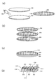
- FIG. 11 illustrates a process of manufacturing a lens that is an optical component having a lens portion having at least one aspherical shape, using the lens array 304 shaped by the process described above.
- the formed lens array is bonded by a method such as bonding a plurality of sheets as necessary (bonding step).
- 11A shows three lens arrays 304 before being joined
- FIG. 11B shows a joined lens array 310 in which three lens arrays 304 are joined.
- the cemented lens array 310 joined in the joining process is divided by a method such as cutting so as to have at least one lens portion (dividing process).
- a lens is manufactured by dividing the cemented lens array 310. If the scribe layer S (see FIG. 2) is formed on the wafer W as described above, the cemented lens array 310 can be easily divided.
- FIG. 11C shows a lens 314 manufactured by cutting the cemented lens array 310 joined so that the lens arrays 304 are laminated so as to include one lens portion 312.
- a camera can be manufactured by attaching the lens 314 to a light receiving element such as a CMOS sensor, for example, and the manufactured camera is used as a camera built in a mobile phone, for example.
- a process of manufacturing a lens 314 having a plurality of lens portions by forming a cemented lens array by joining a plurality of lens arrays 304 and dividing the cemented lens array 310.
- the lens 314 including a single layer can be formed by dividing the plurality of lens arrays 304 without joining them.
- the lens array 304 and the cemented lens array 310 can be used as the lens array 304 and the cemented lens array 310 without being divided.
- the lens array 304 (see FIG. 11) is modeled using the modeling apparatus 10 (see FIG. 1), whereas in the second embodiment, the modeling apparatus 10 is used.
- the mold used to mold the lens array is formed.
- the mold is formed through the placement process in step S100, the photocurable composition application process in step S200, the transfer process in step S300, and the wafer unloading process in step S500. This transfer process is repeated according to the number of lens portions of the lens array to be finally molded.
- the transfer body 62 (see FIG. 2) is a transfer body 62 having a transfer portion processed into a shape opposite to the aspherical lens portion formed on the lens array 304. It was. On the other hand, in the second embodiment, a transfer body 62 having a lens portion processed into the same shape as the lens portion of the lens array finally formed is used. For this reason, the shape of the lens portion 312 of the lens array 304 to be finally formed is transferred to the lens molding die to be shaped.
- a step of forming a lens array as a primary optical component using a mold formed using the modeling apparatus 10 and the molded lens array are divided.
- a process for manufacturing a lens as a secondary optical component is described.
- the model 300 is modeled using the modeling apparatus 10 (modeling).
- the lens array 304 is formed using, for example, a nanoimprint technique (lens array forming step).
- a nanoimprint technique for example, two molds 300 are prepared, and the two molds 300 and 300 are arranged so that the surfaces on which the shape of the transfer body 62 (see FIG. 2) is transferred face each other.
- a lens array material such as a curable composition is supplied using the supply device 302, and the material such as the curable composition is cured in a deformed state according to the shape of the molds 300 and 300, thereby transferring the mold 300.
- a lens array having a shape opposite to the shape of the surface is molded.
- the curable composition can be cured by irradiation with light.
- the two molds 300 are arranged so that the surfaces on which the shape of the transfer body 62 is transferred face each other and the lens array material is supplied between the molds 300, 300.
- a lens array material may be supplied between the mold 300 and the flat plate by disposing the surface on which the shape of the body 62 is transferred and a flat plate having a flat surface.
- the formed lens array is bonded as necessary (joining step) as shown in FIG. 12 (c) is a cemented lens array 310, and the cemented lens array 310 is divided so as to have at least one lens portion (dividing step), and as shown in FIG. 12 (d), A lens 314 having one lens portion 312 is manufactured.
- the lens 314 can be manufactured by attaching the lens 314 to a light receiving element such as a CMOS sensor, for example. Used as a built-in camera.
- the lens array 304 manufactured in the second embodiment can be divided into a single layer without joining, thereby forming a lens 314 composed of a single layer. it can. Further, the lens array 304 and the cemented lens array 310 can be used as the lens array 304 and the cemented lens array 310 without being divided.
- the modeled object that can be modeled using the apparatus 10 is not limited to an optical component such as a lens array or a mold for molding the optical component, but includes, for example, an electroforming mother mold used in electroforming and a tank model. I can give you.
- the curable composition used in the present invention includes a urethane compound having a polymerizable functional group and a polymerization initiator, preferably, (A) silica fine particles, (B) a urethane compound having a specific structure (hereinafter also referred to simply as “urethane compound (B)”), and (C) having an ethylenically unsaturated group and having an alicyclic structure.
- a urethane compound having a polymerizable functional group and a polymerization initiator preferably, (A) silica fine particles, (B) a urethane compound having a specific structure (hereinafter also referred to simply as “urethane compound (B)”), and (C) having an ethylenically unsaturated group and having an alicyclic structure.
- (Meth) acrylate (hereinafter also referred to simply as reactive (meth) acrylate (C)) and (D) a polymerization initiator, and the silica fine particles (A) are surface-treated with a specific silane compound. It is characterized.
- (meth) acrylate means methacrylate and / or acrylate.
- silica fine particles (A) used in the curable composition those having an average particle diameter of 1 to 100 nm can be suitably used.
- the average particle size is less than 1 nm, the viscosity of the prepared curable composition increases, the content of the silica fine particles (A) in the curable composition is limited, and the dispersion in the curable composition is limited.
- a cured product obtained by curing the curable composition hereinafter also simply referred to as a cured product
- sufficient transparency and heat resistance tend to be not obtained.
- the average particle diameter exceeds 100 nm, the transparency of the cured product may deteriorate.
- the average particle diameter of the silica fine particles (A) is preferably 1 to 50 nm, more preferably 5 to 50 nm, and most preferably 5 to 40 nm, from the viewpoint of the balance between the viscosity of the curable composition and the transparency of the cured product. It is.
- the average particle size of the silica fine particles (A) was determined by observing the silica fine particles with a high-resolution transmission electron microscope (type HI-9000, manufactured by Hitachi, Ltd.). A particle image can be selected and obtained as a number average particle size by a known image data statistical processing technique.
- silica fine particles having different average particle diameters may be mixed and used in order to increase the filling amount of the silica fine particles (A) into the cured product.
- silica fine particles (A) porous silica sol, or a composite metal oxide of aluminum, magnesium, zinc or the like and silicon may be used.
- the content of the silica fine particles (A) in the curable composition is preferably 20 to 80% by mass as the surface-treated silica fine particles, and the heat resistance and environmental resistance of the cured product and the viscosity of the curable composition. From the viewpoint of the balance, the amount is more preferably 40 to 60% by mass. Within this range, the fluidity of the curable composition and the dispersibility of the silica fine particles (A) in the curable composition are good. Therefore, if such a curable composition is used, sufficient strength and heat resistance can be obtained. And a cured product having environmental resistance can be easily produced.
- silica fine particles (A) it is preferable to use silica fine particles dispersed in an organic solvent from the viewpoint of dispersibility in the curable composition.
- organic solvent it is preferable to use a solvent in which organic components (such as urethane compound (B) and (meth) acrylate (C) described later) contained in the curable composition are dissolved.
- organic solvent examples include alcohols, ketones, esters, and glycol ethers.
- Methanol, ethanol, isopropyl alcohol, butyl are used because of the ease of solvent removal in the solvent removal step of removing the organic solvent from the mixed liquid of silica fine particles (A), urethane compound (B) and (meth) acrylate (C) described later.
- Alcohol solvents such as alcohol and n-propyl alcohol, and ketone organic solvents such as methyl ethyl ketone and methyl isobutyl ketone are preferred.
- isopropyl alcohol is particularly preferable.
- silica fine particles (A) dispersed in isopropyl alcohol are used, the viscosity of the curable composition after solvent removal is lower than when other solvents are used, and the curable composition having a low viscosity is stabilized. Can be produced.
- silica fine particles dispersed in an organic solvent can be produced by a conventionally known method, and are commercially available, for example, under the trade name Snowtech IPA-ST (manufactured by Nissan Chemical Co., Ltd.).
- distributed to the organic solvent is the silica particle contained in a composition. Refers to the content of itself.
- the silica fine particles (A) used in the curable composition used in the present invention are surface-treated with a silane compound (E).
- a silane compound (E) hereinafter, the silane compound will be described.
- the silane compound (E) is represented by the following general formula (2).
- R 5 represents a hydrogen atom or a methyl group
- R 6 represents an alkyl group having 1 to 3 carbon atoms or a phenyl group
- R 7 represents a hydrogen atom or a hydrocarbon group having 1 to 10 carbon atoms.
- Q is an integer from 1 to 6, and r is an integer from 0 to 2.
- R 6 is a methyl group
- R 7 is a methyl group
- preferable q is 3
- preferable r is 0.
- the silane compound (E) reduces the viscosity of the curable composition and improves the dispersion stability of the silica fine particles (A) in the curable composition by reacting with the urethane compound (B) described later. In addition, it is used for reducing curing shrinkage when curing the curable composition and imparting moldability to the cured product.
- the viscosity of the curable composition is increased, the curing shrinkage at the time of curing is increased, the cured product becomes brittle, and the cured product becomes Since cracks are generated, it is not preferable.
- silane compound (E) examples include ⁇ -acryloxypropyldimethylmethoxysilane, ⁇ -acryloxypropylmethyldimethoxysilane, ⁇ -acryloxypropyldiethylmethoxysilane, ⁇ -acryloxypropylethyldimethoxysilane, and ⁇ -acryloxy.
- ⁇ -acryloxypropyldimethylmethoxysilane and ⁇ -acryloxypropylmethyldimethoxysilane are used.
- ⁇ -methacryloxypropyldimethylmethoxysilane, ⁇ -methacryloxypropylmethyldimethoxysilane, ⁇ -acryloxypropyltrimethoxysilane, and ⁇ -methacryloxypropyltrimethoxysilane are preferable, and ⁇ -acryloxypropyltrimethoxy is more preferable.
- Silane Moreover, these can be used in combination of 2 or more types.
- such a silane compound (E) can be manufactured by a well-known method, and is marketed.
- the amount of the silane compound (E) used in the surface treatment of the silica fine particles (A) is usually 10 to 50 parts by weight, preferably 20 to 40 parts by weight, more preferably 24, to 100 parts by weight of the silica fine particles A). Is 36 parts by mass.
- the amount of the silane compound (E) used is less than 10 parts by mass, the viscosity of the curable composition is increased, the dispersibility of the silica fine particles (A) in the curable composition is deteriorated, and gelation occurs. there is a possibility.
- silica fine particle (A) when it exceeds 50 mass parts, aggregation of a silica fine particle (A) may be caused.
- the mass of the said silica particle (A) points out the mass of only the silica particle itself disperse
- the silane compound (E) When a large amount of acrylate (urethane compound (B) and reactive acrylate (C) described later) is contained in the curable composition, the silane compound (E) has an acrylic group, that is, R 1 is a hydrogen atom.
- the silane compound represented by the general formula (1) and the curable composition contain a large amount of methacrylate (urethane compound (B) and methacrylate (C) described later), as the silane compound (E), It is preferable to use a silane compound represented by the general formula (1) containing a methacryl group, that is, R 1 is a methyl group. In such a case, a curing reaction tends to occur when the curable composition of the present invention is cured.
- the (B) urethane compound used in the present invention (hereinafter also referred to simply as “(B) urethane compound”) is represented by the following general formula (1), and contains two or more polymerizable unsaturated bonds in the molecule. To do.
- R 1 represents a linear or branched divalent aliphatic group having 1 to 12 carbon atoms, a divalent organic group having 3 to 12 carbon atoms having an alicyclic group, and an aromatic ring.
- R 1 is the viewpoint of curability of the curable composition of the present invention described later, and the hardness and curl of a cured product obtained by curing the curable composition (hereinafter also simply referred to as “cured product”).
- a divalent aliphatic group having 1 to 6 carbon atoms or [— (CH 2 ) a —O— (CH 2 ) b —] c (a and b are each independently an integer of 1 to 5; c is preferably an integer of 1 to 3, and a divalent aliphatic group having 2 to 4 carbon atoms or [— (CH 2 ) a —O— (CH 2 ) b —] c (a And b are each independently an integer of 2 to 4, and c is 1 or 2.), more preferably a divalent aliphatic group having 2 or 3 carbon atoms, or — (CH 2 ) 2 —O—. More preferred is (CH 2 ) 2 —.
- R 2 represents a linear or branched divalent aliphatic group having 1 to 10 carbon atoms, a divalent organic group having 3 to 10 carbon atoms having an alicyclic group, and an aromatic ring. Or a divalent organic group having 6 to 30 carbon atoms or [— (CH 2 ) d —O— (CH 2 ) e —] f (where d and e are each independently an integer of 1 to 10, f Represents an integer of 1 to 5.
- R 2 has 1 to 6 carbon atoms from the viewpoint of the balance between the curability of the curable composition of the present invention, which will be described later, and the hardness and curl properties of a cured product obtained by curing the curable composition.
- a divalent aliphatic group having 2 to 4 carbon atoms a divalent organic group having 6 to 30 carbon atoms having a benzene ring, or [— (CH 2 ) d —O— (CH 2 ) e ⁇ ] f (d and e are each independently an integer of 2 to 4, f represents 1 or 2), and is a divalent aliphatic group having 2 or 3 carbon atoms or — (CH 2 ) 2 —O— (CH 2 ) 2 — is more preferable.
- R 3 and R 4 are each independently a hydrogen atom or a methyl group. From the viewpoint of curability of curing at a low exposure amount, a hydrogen atom is preferable.
- a cured product having an excellent balance of surface hardness, transparency and curling property can be obtained. That is, high quality is achieved for various products made of the cured product of the present invention.
- the content of the (B) urethane compound is preferably 10 to 99 parts by mass, more preferably 20 to 99 parts by mass, and further preferably 30 to 99 parts by mass.
- the content of the urethane compound is within the above range, a resin excellent in curability, pencil hardness, scratch resistance, curling property, balance of strength and flexibility can be obtained.
- the urethane compound represented by the general formula (1) used in the present invention is a polymerizable unsaturated group-containing alcohol compound represented by the following general formula (3) (hereinafter also referred to as “compound (1)”). It can be synthesized by contacting with a polymerizable unsaturated group-containing isocyanate compound represented by the following general formula (4) (hereinafter also referred to as “compound (2)”).
- R 1 and R 3 are the same as described above.
- R 2 and R 4 are the same as described above.
- Examples of the compound (1) include 2-hydroxyethyl (meth) acrylate, 2-hydroxypropyl (meth) acrylate, 3-hydroxypropyl (meth) acrylate, 4-hydroxybutyl (meth) acrylate, and the like. These can be used individually by 1 type or in combination of 2 or more types. 2-Hydroxyethyl (meth) acrylate is preferred.
- R 3 is a hydrogen atom, that is, when the compound (1) has an acrylate structure
- R 3 is a methyl group, that is, when the compound (1) has a methacrylate structure
- (meth) acrylate means methacrylate and / or acrylate.
- OCN-R 2 in the general formula (4) an isocyanate compound containing one or more unsaturated groups in the molecule represented by - for R 2, the same as R 2 in the compound represented by the general formula (1)
- specific examples of OCN—R 2 — include the following (a) to (e).
- * is a structure containing an isocyanate group, hydrogen, a (meth) acryl group, a hydrocarbon group, or an aromatic ring. Each * may be the same or different.
- (A) is a structure containing a divalent saturated aliphatic group, alicyclic group or aromatic ring having a linear or branched structure, and h is that the number of carbon atoms in the portion excluding the isocyanate group is 1-10. An integer that satisfies the condition.
- (B) is a structure containing a divalent saturated aliphatic group, alicyclic group or aromatic ring having a linear or branched structure, and l is said to have 1 to 10 carbon atoms in the portion excluding the isocyanate group.
- (C) is a structure having a cyclohexane ring as a main skeleton, and the carbon number of the portion excluding the isocyanate group is 6 or more and 10 or less.
- (D) is a structure having a benzene ring as the main skeleton, and the carbon number of the portion excluding the isocyanate group is 6 or more and 10 or less.
- (E) is a structure having an ether skeleton, and i, j, and k are integers that satisfy the condition that the number of carbon atoms in the portion excluding the isocyanate group is 1 or more and 100 or less.
- R 4 is a hydrogen atom or a methyl group, preferably a hydrogen atom.
- Preferred specific examples of the compound (2) are shown below. Examples of those having the structure (a) include 2- (meth) acryloyloxyethyl isocyanate, 3- (meth) acryloyloxypropyl isocyanate, 4- (meth) acryloyloxybutyl isocyanate, and 5- (meth) acryloylpentyl isocyanate.
- 6- (meth) acryloyloxyhexyl isocyanate, 2- (meth) acryloyloxypropyl isocyanate, 1,1-bis (acryloyloxymethyl) ethyl isocyanate, and those having the structure of (b) above are 3-isocyanato- Examples of 2-methylpropyl (meth) acrylate having the structure (c) include 3-isocyanatocyclohexyl (meth) acrylate, 4-isocyanatocyclohexyl (meth) acrylate, and the structure (d) above.
- a urethanization catalyst By using the urethanization catalyst, the reaction can be remarkably accelerated.
- Specific examples of the urethanization catalyst include dibutyltin dilaurate, copper naphthenate, cobalt naphthenate, zinc naphthenate, triethylamine, 1,4-diazabicyclo [2.2.2] octane, 2,6,7-trimethyl-1 , 4-diazabicyclo [2.2.2] octane.
- the urethanization catalysts may be used alone or in combination of two or more.
- the addition amount of the urethanization catalyst is preferably 0.01 to 5 parts by mass, more preferably 0.1 to 1 part by mass with respect to 100 parts by mass of the compound (2). If the addition amount is less than 0.01 parts by mass, the reactivity may decrease. On the other hand, when the addition amount exceeds 5 parts by mass, a side reaction may occur during the reaction.
- the reaction temperature in the reaction between the compound (1) and the compound (2) is preferably ⁇ 10 to 100 ° C., more preferably 0 to 60 ° C. More preferably, it is 10 to 30 ° C.
- the above reaction can be carried out in hexane containing BHT (2,6-di-tert-butyl-4-methylphenol). Since BHT-containing hexane can be used as a cleaning solvent as it is after completion of the reaction, it is possible to reduce the burden on the environment when performing the above reaction.
- the content of BHT in the BHT-containing hexane is 1 to 1000 ppm, preferably 50 to 500 ppm, and more preferably 100 to 400 ppm.
- cyclohexyl (meth) acrylate 4-butylcyclohexyl (meth) acrylate, dicyclopentanyl (meth) acrylate, dicyclopentenyl (meth) acrylate, dicyclopentadienyl (meth) acrylate, bornyl (meth) acrylate, Cycloalkyls such as isobornyl (meth) acrylate, tricyclodecanyl (meth) acrylate, adamantyl (meth) acrylate, dicyclopentanyl di (meth) acrylate, tricyclodecane dimethanol diacrylate, adamantyl di (meth) acrylate, etc. And (meth) acrylates.
- (meth) acrylate having two ethylenically unsaturated groups is preferable, and dicyclopentanyl di (meth) acrylate is most preferable, from the viewpoint of shape followability to the mold. .
- the alicyclic structure is a structure in which an aromatic ring structure is excluded from a structure in which carbon atoms are bonded cyclically.
- the amount of (meth) acrylate (C) used in the curable composition is preferably 5 to 400 parts by weight, more preferably 10 parts per 100 parts by weight of the silica fine particles (A) before the surface treatment. Is 200 parts by mass, more preferably 20-100 parts by mass.
- the blending amount is less than 5 parts by mass, the shape following property to the mold is lowered. If the blending amount exceeds 400 parts by mass, the adhesion to the substrate may be lowered.
- the mass of the said silica particle (A) points out the mass of only the silica particle itself disperse
- photopolymerization initiator examples include benzophenone, benzoin methyl ether, benzoin propyl ether, diethoxyacetophenone, 1-hydroxy-phenylphenyl ketone, 2,6-dimethylbenzoyldiphenylphosphine oxide, 2,4,6-trimethylbenzoyldiphenyl. And phosphine oxide and diphenyl- (2,4,6-trimethylbenzoyl) phosphine oxide. Two or more of these photopolymerization initiators may be used in combination.
- the content of the photopolymerization initiator in the curable composition may be an amount that allows the curable composition to be appropriately cured, and is 0.01 to 10 parts by mass with respect to 100 parts by mass of the curable composition. It is preferably 0.02 to 5 parts by mass, more preferably 0.1 to 2 parts by mass. If the addition amount of the photopolymerization initiator is too large, the storage stability of the curable composition is lowered, colored, or the crosslinking at the time of crosslinking to obtain a cured product rapidly proceeds, such as cracks during curing. Problems may occur. Moreover, when there are too few addition amounts of a photoinitiator, a curable composition may not fully be hardened.
- thermal polymerization initiator examples include benzoyl peroxide, diisopropyl peroxycarbonate, t-butyl peroxy (2-ethylhexanoate) and the like.
- the content of the thermal polymerization initiator in the curable composition is preferably 2 parts by mass or less, more preferably 0.1 to 2 parts by mass with respect to 100 parts by mass of the curable composition.
- the curable composition used in the present invention is, as necessary, a leveling agent, an antioxidant, and an ultraviolet absorber as long as the viscosity of the composition and the properties of the cured product, such as transparency and heat resistance, are not impaired.
- a leveling agent such as acrylic acid, acrylic acid, and the like.
- an antioxidant such as sodium metabisulfite, sodium metabisulfite, sodium metabisulfite, sodium metabisulfite, sodium metabisulfite, sodium metabisulfite, sodium metabisulfite, sodium metabisulfite, sodium metabisulfite, sodium metabisulfite, sodium metabisulfite, sodium metabisulfite, sodium metabisulfite, sodium metabisulfite, sodium metabisulfite, sodium metabisulfite, sodium metabisulfite, sodium metabisulfite, sodium metabisulfite, sodium metabisulfite, sodium metabisulfite, sodium metabisulfite, sodium metabisulfite, sodium metabisulfite, sodium
- leveling agents include polyether-modified dimethylpolysiloxane copolymer, polyester-modified dimethylpolysiloxane copolymer, polyether-modified methylalkylpolysiloxane copolymer, aralkyl-modified methylalkylpolysiloxane copolymer, and polyether-modified. Examples thereof include methylalkylpolysiloxane copolymer.
- filler or pigment examples include calcium carbonate, talc, mica, clay, Aerosil (registered trademark), barium sulfate, aluminum hydroxide, zinc stearate, zinc white, bengara, azo pigment, and the like.
- Corn-type viscometer DV-IIIULTRA manufactured by BROOKFIELD
- 25 ° C. spindle no.
- the viscosity measured with CP-41 is usually 100 to 5000 mPa ⁇ s, and it has a low viscosity even without containing a solvent and has good handling properties.
- the silica fine particles (A) are highly compatible with the urethane compound (B) and the (meth) acrylate (C) by the surface treatment of the silica fine particles (A), and the urethane compounds (B) and (meth). This is due to the high dispersion stability of the silica fine particles (A) in the acrylate (C).
- the curable composition used in the present invention includes, for example, a step of surface-treating colloidal silica (silica fine particles (A)) dispersed in an organic solvent with a silane compound (E) (step 1), and surface-treated silica fine particles.
- Step 2 in which urethane compound (B) and (meth) acrylate (C) are added to (A) and uniformly mixed, silica fine particles (A) obtained in Step 2, urethane compound (B) and (Metal) )
- step 1 the silica fine particles (A) are surface-treated with the silane compound (E).
- the silica fine particles (A) are put in a reactor, and while stirring, the silane compound (E) is added, stirred and mixed, and water and a catalyst necessary for hydrolyzing the silane compound are further added. While stirring, the silane compound is hydrolyzed and subjected to condensation polymerization on the surface of the silica fine particles (A).
- silica fine particles dispersed in an organic solvent as the silica fine particles (A).
- the disappearance due to hydrolysis of the silane compound can be confirmed by gas chromatography.
- a non-polar column DB-1 manufactured by J & W
- gas chromatography Alignment Co., Ltd. Model 6850
- temperature 50 to 300 ° C. heating rate 10 ° C./min
- He He
- the residual amount of the silane compound can be measured by an internal standard method with a flow rate of 1.2 cc / min and a flame ionization detector, disappearance due to hydrolysis of the silane compound can be confirmed.
- the amount of the silane compound (E) used in the surface treatment of the silica fine particles (A) is usually 10 to 50 parts by mass, preferably 20 to 40 parts by mass with respect to 100 parts by mass of the silica fine particles (A). Part by mass, more preferably 24 to 36 parts by mass.
- the lower limit of the amount of water required for carrying out the hydrolysis reaction is 1 times the total number of moles of alkoxy groups and hydroxy groups bonded to the silane compound (E), and the upper limit is 10 times. If the amount of water is too small, the hydrolysis rate may become extremely slow, resulting in lack of economic efficiency, or the surface treatment may not proceed sufficiently. Conversely, if the amount of water is excessively large, the silica fine particles (A) may form a gel.
- a catalyst for the hydrolysis reaction When performing the hydrolysis reaction, a catalyst for the hydrolysis reaction is usually used.
- a catalyst include, for example, inorganic acids such as hydrochloric acid, acetic acid, sulfuric acid, phosphoric acid; Organic acids such as formic acid, propionic acid, oxalic acid, p-toluenesulfonic acid, benzoic acid, phthalic acid, maleic acid; Alkali catalysts such as potassium hydroxide, sodium hydroxide, calcium hydroxide, ammonia; organic metals; Metal alkoxides; Organotin compounds such as dibutyltin dilaurate, dibutyltin dioctylate, dibutyltin diacetate; Aluminum tris (acetylacetonate), titanium tetrakis (acetylacetonate), titanium bis (butoxy) bis (acetylacetonate), titanium bis (isopropoxy) bis (acetylacetonate), zir
- hydrochloric acid, acetic acid, maleic acid, and boron compounds are preferable from the viewpoints of solubility in water and sufficient hydrolysis rate.
- These catalysts can be used alone or in combination of two or more.
- Step 1 when the hydrolysis reaction of the silane compound (E) is performed, a water-insoluble catalyst may be used, but a water-soluble catalyst is preferably used.
- a water-soluble catalyst for hydrolysis reaction it is preferable to dissolve the water-soluble catalyst in an appropriate amount of water and add it to the reaction system because the catalyst can be uniformly dispersed.
- the addition amount of the catalyst used for the hydrolysis reaction is not particularly limited, but usually silica fine particles (a ) 0.1 to 10 parts by weight, preferably 0.5 to 5 parts by weight per 100 parts by weight.
- distributed to the organic solvent as a silica particle (A)
- the mass of the said silica particle (A) points out the mass of only the silica particle itself disperse
- the reaction temperature of the hydrolysis reaction is not particularly limited, but is usually in the range of 10 to 80 ° C, preferably in the range of 20 to 50 ° C. If the reaction temperature is excessively low, the hydrolysis rate may become extremely slow, resulting in lack of economic efficiency, and the surface treatment may not proceed sufficiently. When the reaction temperature is excessively high, the gelation reaction tends to occur.
- the reaction time for performing the hydrolysis reaction is not particularly limited, but is usually in the range of 10 minutes to 48 hours, preferably 30 minutes to 24 hours.
- the method of mixing the surface-treated silica fine particles (A) with the urethane compound (B) and (meth) acrylate (C) is not particularly limited.
- a mixer a ball mill at room temperature or under heating conditions.
- a method of mixing with a mixer such as a three-roller, or a method of adding and mixing the urethane compound (B) and (meth) acrylate (C) while continuously stirring in the reactor in which Step 1 was performed. Can be mentioned.
- step 3 the organic solvent and water are distilled off from the homogeneous mixture of silica fine particles (A), urethane compound (B) and (meth) acrylate (C), and the solvent is removed (hereinafter collectively referred to as solvent removal). It is preferable to heat in a reduced pressure state.
- the temperature is preferably maintained at 20 to 100 ° C., and more preferably 30 to 70 ° C., and further preferably 30 to 50 ° C. in terms of the balance between aggregation gelation prevention and the solvent removal speed. If the temperature is raised too much, the fluidity of the curable composition may be extremely lowered, or the curable composition may be gelled.
- the degree of vacuum at the time of depressurization is usually 10 to 4000 kPa, more preferably 10 to 1000 kPa, and most preferably 10 to 500 kPa in order to balance the solvent removal speed and the prevention of aggregation gelation. If the value of the degree of vacuum is too large, the solvent removal speed becomes extremely slow, which is economical.
- the composition after desolvation contains substantially no solvent.
- substantially means that when a cured product is actually obtained using the curable composition, it is not necessary to go through a step of removing the solvent again.
- the remaining amount of the organic solvent and water in the product is preferably 1% by mass or less, preferably 0.5% by mass or less, and more preferably 0.1% by mass or less.
- a polymerization inhibitor may be added to 100 parts by mass of the composition after desolvation before desolvation.
- the polymerization inhibitor is used to prevent components contained in the composition from undergoing a polymerization reaction during the solvent removal process or during storage of the composition after the solvent removal and the curable composition.
- the polymerization inhibitor include hydroquinone, hydroquinone monomethyl ether, benzoquinone, pt-butylcatechol, 2,6-di-tert-butyl-4-methylphenol, and the like. These can be used alone or in combination of two or more.
- Step 3 can be carried out by transferring the homogeneous mixed liquid of silica fine particles (A), urethane compound (B) and (meth) acrylate (C), which has undergone Step 2, to a dedicated apparatus. If carried out in the reactor in which 1 was carried out, it can be carried out in the reactor following step 2.
- Step 4 the method of adding the polymerization initiator (D) to the composition desolvated in Step 3 and uniformly mixing the mixture is not particularly limited.
- a mixer such as a mixer, a ball mill, or a three roll at room temperature.
- This filtration is performed for the purpose of removing foreign substances such as dust in the curable composition.
- the filtration method is not particularly limited, but a pressure filtration method using a membrane type or cartridge type filter having a pressure filtration pore size of 1.0 ⁇ m is preferred.
- the curable composition used in the present invention is cured to cure an optical lens, an optical lens mold, an optical disk substrate, a liquid crystal display element plastic substrate, a color filter substrate, an organic EL display element plastic substrate, and a solar cell. It becomes the hardened
- the curing shrinkage rate is small, it can be used as a mold for various moldings, and in particular, a cured product that can be suitably used as a mold used for molding optical components such as lens arrays.
- a cured product is obtained by curing the curable composition used in the present invention.
- a curing method a method of crosslinking the ethylenically unsaturated groups of the urethane compound (B) and (meth) acrylate (C) by irradiation with active energy rays, a method of thermally polymerizing the ethylenically unsaturated groups by applying heat. These can be used in combination.
- a photopolymerization initiator is contained in the curable composition in the above step 4.
- a thermal polymerization initiator is contained in the curable composition.
- the cured product of the curable composition used in the present invention is formed by, for example, applying the curable composition onto a substrate such as a glass plate, a plastic plate, a metal plate, or a silicon wafer to form a coating film, and then curing the curable composition. It can be obtained by irradiating the active composition with active energy rays or by heating. For curing, both irradiation with active energy rays and heating may be performed.
- Examples of the method for applying the curable composition include application by a bar coater, applicator, die coater, spin coater, spray coater, curtain coater, roll coater, etc., application by screen printing, and application by dipping.
- the coating amount of the curable composition used in the present invention on the substrate is not particularly limited, and can be appropriately adjusted according to the purpose.
- the film thickness of the coating film obtained after the curing treatment by active energy ray irradiation and / or heating is preferably 1 to 200 ⁇ m, and more preferably 5 to 100 ⁇ m.
- the active energy ray used for curing is preferably an electron beam or light in the ultraviolet to infrared wavelength range.
- the light source for example, an ultra-high pressure mercury light source or a metal halide light source can be used for ultraviolet rays, a metal halide light source or a halogen light source can be used for visible rays, and a halogen light source can be used for infrared rays. Can be used.
- the irradiation amount of the active energy ray is appropriately set according to the type of the light source, the film thickness of the coating film, etc., but preferably the reaction of the ethylenically unsaturated group of the urethane compound (B) and (meth) acrylate (C).
- the rate can be appropriately set so as to be 80% or more, more preferably 90% or more.
- curing may be further advanced by heat treatment (annealing treatment).
- the heating temperature at that time is preferably in the range of 80 to 200 ° C.
- the heating time is preferably in the range of 10 minutes to 60 minutes.
- the heating temperature is preferably in the range of 80 to 200 ° C, more preferably in the range of 100 to 150 ° C. .
- the heating temperature is lower than 80 ° C., it is necessary to lengthen the heating time, and there is a tendency that it is not economical. Therefore, it tends to lack economic efficiency.
- the heating time is appropriately set according to the heating temperature, the film thickness of the coating film, etc., but preferably the reaction rate of ethylenically unsaturated groups of urethane compound (B) and (meth) acrylate (C) is 80% or more. More preferably, it can be appropriately set to be 90% or more.
- the heating temperature at that time is preferably in the range of 150 to 200 ° C.
- the heating time is preferably in the range of 5 minutes to 60 minutes.
- the cured product of the curable composition used in the present invention is excellent in transparency, curability, shape followability, and substrate adhesion, it molds a mold used for molding optical components such as lens arrays. Can be suitably used.
- the light transmittance at a wavelength of 400 nm when the cured film is 100 ⁇ m thick is preferably 85% or more.
- the efficiency of utilizing light is lowered, and therefore, the curability at the time of photocuring may be impaired, which is not preferable.
- the curability is poor, the part in contact with the air will not cure due to oxygen inhibition, so the desired shape may not be obtained, or a large amount of light irradiation energy will be required to cure, or heating Although it takes a long time, it is not preferable from the viewpoint of productivity.
- the cured product is excellent in curability, it is easily cured without being inhibited by oxygen when it is photocured or thermally cured in air. Can be obtained.
- the cured product is cured in a state where a curable composition is applied on a substrate such as glass, a transfer body is in contact with the curable composition, and the curable composition is deformed according to the shape of the transfer body.
- the transfer composition formed on the transfer body which is obtained by curing the curable composition by irradiating light or the like, is transferred to the cured product.
- cured material is excellent in the shape followability to a transfer body.
- “excellent in shape following” means that the shape of the transfer body is transferred as it is as the shape of the cured product, and the surface of the cured product is less likely to be wrinkled or cracked.
- the cured product is coated with a curable composition on a substrate such as glass, the transfer body comes into contact with the curable composition, and the curable composition is deformed according to the shape of the transfer body.
- the composition is separated from the transfer body.
- the cured product has excellent substrate adhesion. If the substrate adhesion is inferior, the cured product is brought to the transfer body side and the cured product is peeled off from the substrate, which is not preferable because it does not function as a mold used for molding optical components, for example.
- curable composition used for this invention is demonstrated in detail by an Example, this curable composition is not limited to the following examples, unless the summary is exceeded.
- a urethane compound (B-2) was obtained.
- [Preparation of curable composition] (Preparation Example 1) In a separable flask, 100 parts by mass of isopropyl alcohol-dispersed colloidal silica (silica content 30% by mass, average particle size 10-20 nm, trade name Snowtech IPA-ST; manufactured by Nissan Chemical Co., Ltd.) is placed. In addition, 9.0 parts by mass of ⁇ -methacryloxypropyltrimethoxysilane was added, and mixed by stirring. Further, 2.9 parts by mass of a 0.1825% by mass HCl solution was added, and the mixture was stirred at 20 ° C. for 24 hours to obtain silica fine particles. Surface treatment was performed.
- urethane compound (B-1) and dicyclopentadienyl diacrylate (trade name: Light acrylate DCP-A; manufactured by Kyoeisha Chemical Co., Ltd.) 14.7 are applied to the silica fine particles subjected to surface treatment. Part by mass was added and mixed uniformly. Thereafter, the mixture was heated under reduced pressure at 40 ° C. and 100 kPa with stirring to remove volatile components. The amount of volatile matter removed was 72.0 parts by mass.
- a curable composition 4 was prepared in the same manner as Preparation Example 1 except that ethyladamantyl acrylate (manufactured by Osaka Organic Chemical Co., Ltd., trade name EtADA) was used instead of the urethane compound (B-1). Obtained.
- the viscosity of this curable composition 4 was 4100 mPa ⁇ S.
- composition of each component used for the preparation of the above curable composition is shown in Table 1 below.
- the curable composition is injected onto the wafer W using an injection device, and the transfer body is in contact with the photocurable composition with respect to the curable composition such that the convex portions 90 are in contact with the photocurable composition.
- No. 62 was brought into contact, and was exposed to 4 J / cm 2 with an exposure apparatus incorporating an ultrahigh pressure mercury lamp and cured. Thereafter, the transfer body 62 was separated from the wafer W. The above operation was repeated 100 times to obtain a cured product in which the shape of 100 transfer bodies 62 was transferred. The shape of these 100 cured products was observed with an optical microscope, and the presence or absence of wrinkles or cracks was evaluated.
- the evaluation criteria are as follows, and the results are shown in Table 2.
- the curable composition is injected onto the wafer W using an injection device, and the transfer body is in contact with the photocurable composition with respect to the curable composition such that the convex portions 90 are in contact with the photocurable composition.
- No. 62 was brought into contact, and was exposed to 4 J / cm 2 with an exposure apparatus incorporating an ultrahigh pressure mercury lamp and cured. Thereafter, the transfer body 62 was separated from the wafer W. The above operation was repeated 100 times.
- the transfer body 62 is separated from the wafer W and the substrate adherence of the cured product is poor, the cured product adheres to the transfer body 62 side and peels off from the wafer W.
- Table 2 shows the results of evaluating the number obtained by closely contacting the wafer W in 100 cured products as the substrate adhesion. For example, when 90 of 100 pieces are in close contact with the wafer W, the evaluation result is expressed as 90/100.
- the curable compositions of Preparation Examples 1 and 2 are excellent in shape followability, substrate adhesion, and transparency. Therefore, in order to mold a mold used for molding an optical component such as a lens array. It can be used suitably.
- the curable composition of Comparative Example Preparation 1 is excellent in adhesion to the substrate and transparency, but is inferior in shape following property and may cause wrinkles and cracks.
- the curable composition of Comparative Preparation Example 2 is excellent in transparency, it is inferior in shape followability and substrate adhesion, and may be peeled off from the substrate. , Because wrinkles and cracks may occur.
- FIG. 10 When the steps shown in FIG. 10, FIG. 11 and FIG. 12 were performed using the curable compositions 1 and 2 produced by the methods shown in Preparation Examples 1 and 2 of the curable composition, a good lens was obtained. A mold used for molding arrays and lenses could be obtained. In particular, with respect to modeling of a mold used for molding a lens, both shape following and substrate adhesion were good.
- the present invention is applied to, for example, a modeling method for modeling a lens such as a lens array having a lens portion having an aspherical shape, or a model such as a mold used for molding such a lens. be able to.
Landscapes
- Engineering & Computer Science (AREA)
- Mechanical Engineering (AREA)
- Addition Polymer Or Copolymer, Post-Treatments, Or Chemical Modifications (AREA)
- Casting Or Compression Moulding Of Plastics Or The Like (AREA)
- Shaping Of Tube Ends By Bending Or Straightening (AREA)
- Macromonomer-Based Addition Polymer (AREA)
Abstract
従来の技術と比較して、レンズ等の造形物を高精度に造形することができる造形方法を提供する。重合性官能基を有するウレタン化合物と重合開始剤とを含む光硬化性組成物と、非球面形状からなるレンズ部(312)と同形状、又は非球面形状からなるレンズ部(312)と反対形状からなる転写形状部が形成された転写体(62)とを互いに接触させ、光硬化性組成物を転写体(62)の転写形状にならって変形させる変形工程と、変形した光硬化性組成物の少なくとも変形した部分を、光照射装置(60)で光を照射することで硬化させる硬化工程と、硬化した光硬化性組成物と転写部材とを離間させる離間工程とからなる転写工程を複数回繰り返して、レンズアレイ、ナノインプリント用の型等の造形物を造形する。
Description
本発明は、例えば、非球面形状からなるレンズ部を有するレンズアレイ等のレンズや、このようなレンズの成形に用いられる型等の造形物を造形する造形方法に関する。
特許文献1には、レンズ形状を形成する面を有する金型を用いたマイクロレンズアレイの製造方法であって、前記金型により第1の基板上に第1の樹脂を前記レンズ形状に硬化させレンズ基板を複数形成する工程と、前記レンズ基板をアレイ状に配列する工程と、前記アレイ状のレンズ基板上にメッキして前記レンズ形状を形成する面を有するマスタを形成する工程と、前記マスタのレンズ形状を形成する面上にメッキしてマザーを形成する工程と、前記マザーにより成形型を形成する工程と、前記成形型により第2の基板上に第2の樹脂を前記レンズ形状に硬化させ形成する工程と、ドライエッチングにより前記第2の
樹脂を除去するとともに前記第2の基板の一部を除去する工程とを含むマイクロレンズアレイの製造方法が開示されている。
樹脂を除去するとともに前記第2の基板の一部を除去する工程とを含むマイクロレンズアレイの製造方法が開示されている。
また、特許文献2には、マザースタンパの表面にある微細パターンを順次転写させることによる微細構造体の製造方法であって、(1) 基板に対して前記マザースタンパを所定の位置に固定する工程と、(2) 前記マザースタンパと前記基板との間に樹脂を供給する工程と、(3) 真空中にて前記マザースタンパを前記樹脂に押圧する工程と、(4) 前記樹脂を硬化させる工程と、(5) 前記マザースタンパを前記硬化樹脂から離脱させる工程と、(6) 前記マザースタンパと前記基板との相対位置を変更させるように、前記マザースタンパ若しくは前記基板を移動させる工程と、(7) 前記工程(6)の後、工程(2)~工程(6)を所定の回数繰り返す工程と、を含む微細構造体の製造方法が開示されている。
しかしながら、特許文献1及び特許文献2に開示の技術では、例えば非球面形状からなるレンズ等の高度な精度が要求される造形物を成形することは困難であるとの問題点があった。
本発明は、従来の技術と比較して、レンズ等の造形物を高精度に造形することができる造形方法を提供することを目的とする。
本発明の特徴とするところは、被造形物と、非球面形状からなるレンズ部と同形状、又は前記非球面形状からなるレンズ部と反対形状からなる転写形状が形成された転写体とを互いに接触させ、被造形物を前記転写形状にならって変形させる変形工程と、被造形物の、少なくとも変形した部分を硬化させる硬化工程と、被造形物と前記転写体とを互いに離間させる離間工程と、前記転写体を前記被造形物の他の位置へ相対移動させる移動工程と、を有し、被造形物に前記転写形状を転写する転写工程を複数回繰り返す造形方法であって、前記被造形物が、重合性官能基を有するウレタン化合物と重合開始剤とを含む硬化性組成物からなる造形方法にある。
好適には、前記硬化性組成物は、
(A)シリカ微粒子と、
(B)下記一般式(1)で表されるウレタン化合物と、
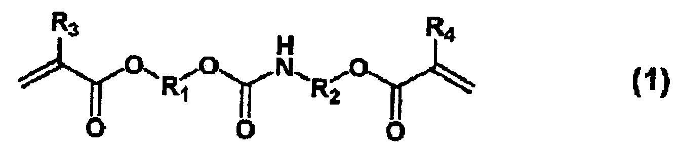
(式中、R1は、直鎖もしくは分岐を有する炭素数1~12の2価の脂肪族基、脂環基を有する炭素数3~12の2価の有機基、芳香環を有する炭素数6~30の2価の有機基または[-(CH2)a-O-(CH2)b-]c(aおよびbはそれぞれ独立に1~10の整数、cは1~5の整数を表す。)であり、
R2は、直鎖もしくは分岐を有する炭素数1~10の2価の脂肪族基、脂環基を有する炭素数3~10の2価の有機基、芳香環を有する炭素数6~30の2価の有機基または[-(CH2)d-O-(CH2)e-]f(dおよびeはそれぞれ独立に1~10の整数、fは1~5の整数を表す。)であり、
R3およびR4はそれぞれ独立に水素原子またはメチル基である。)
(C)エチレン性不飽和基を有し且つ脂環式構造を有する(メタ)アクリレートと、
(D)重合開始剤と
を含み、
前記シリカ微粒子(A)が、下記一般式(2)で表されるシラン化合物(E)で表面処理されていることを特徴とする、請求項1に記載の造形方法。

(式(2)中、R5は水素原子又はメチル基を表し、R6は炭素数1~3のアルキル基又はフェニル基を表し、R7は水素原子又は炭素数1~10の炭化水素基を表し、qは1~6の整数であり、rは0~2の整数である。)
(A)シリカ微粒子と、
(B)下記一般式(1)で表されるウレタン化合物と、
R2は、直鎖もしくは分岐を有する炭素数1~10の2価の脂肪族基、脂環基を有する炭素数3~10の2価の有機基、芳香環を有する炭素数6~30の2価の有機基または[-(CH2)d-O-(CH2)e-]f(dおよびeはそれぞれ独立に1~10の整数、fは1~5の整数を表す。)であり、
R3およびR4はそれぞれ独立に水素原子またはメチル基である。)
(C)エチレン性不飽和基を有し且つ脂環式構造を有する(メタ)アクリレートと、
(D)重合開始剤と
を含み、
前記シリカ微粒子(A)が、下記一般式(2)で表されるシラン化合物(E)で表面処理されていることを特徴とする、請求項1に記載の造形方法。
好適には、前記硬化性組成物に含まれる前記シリカ微粒子(A)が、該シリカ微粒子(A)100質量部に対して10~50質量部の前記シラン化合物(E)で表面処理されている。
好適には、前記硬化性組成物の粘度が100~5000mPa・sである。
本発明によれば、従来の技術と比較して、レンズ等の造形物を高精度に造形することができる造形方法を提供することができる。
10 造形装置
14 支持台
18 駆動源
24 可動台
32 y軸モータ
34 θ軸モータ
36 供給装置
44 可動ユニット
56 x軸モータ
60 光照射装置
62 転写体
64 支持部材用z軸モータ
68 光ファイバー
70 光源
72 検知装置
74 撮影部
76 レンズユニット
90 凸部
200 制御装置
204 主制御部
300 型
304 レンズアレイ
310 接合レンズアレイ
312 レンズ部
314 レンズ
W ウエハ
W1 基板
W2 保持板
h1 貫通孔
h2 孔
14 支持台
18 駆動源
24 可動台
32 y軸モータ
34 θ軸モータ
36 供給装置
44 可動ユニット
56 x軸モータ
60 光照射装置
62 転写体
64 支持部材用z軸モータ
68 光ファイバー
70 光源
72 検知装置
74 撮影部
76 レンズユニット
90 凸部
200 制御装置
204 主制御部
300 型
304 レンズアレイ
310 接合レンズアレイ
312 レンズ部
314 レンズ
W ウエハ
W1 基板
W2 保持板
h1 貫通孔
h2 孔
次に本発明の実施形態を図面に基づいて説明する。
図1において、本発明の第1の実施形態に係る造形装置10が示されている。造形装置10は、造形物であり、光学部品であるレンズアレイの造形に用いられ、設置面に設置される基台12を有し、基台12の上に可動台24が支持されている。可動台24の上側面には、さらに支持台14が支持されている。
図1において、本発明の第1の実施形態に係る造形装置10が示されている。造形装置10は、造形物であり、光学部品であるレンズアレイの造形に用いられ、設置面に設置される基台12を有し、基台12の上に可動台24が支持されている。可動台24の上側面には、さらに支持台14が支持されている。
可動台24は、下側に突出した形状の突出部25が形成された下側部分26と、下側部分26の上側に位置する上側部分27とからなり、突出部25が基台12の上向きの面12aに形成されたy軸方向の溝(不図示)に嵌め込まれるように基台12に取り付けられている。このため、y軸方向の溝にガイドされ、可動台24は、面12a上でy軸方向に移動可能となっている。突出部25には、送りネジ28が噛み合っている。送りねじ28は、軸の方向(長手方向)がy軸方向となるように、軸受30、30を用いて基台12に回動自在に支持されている。送りネジ28の図1における左端部には、基台12に固定さ
れたy軸モータ32が連結されている。したがって、y軸モータ32を回転させることで、送りネジ28を介して突出部25に駆動が伝達され、可動台24がy軸方向に移動する。可動台をy軸のいずれの方向に移動させるかは、y軸モータ32の回転方向を制御することで決することができる。
れたy軸モータ32が連結されている。したがって、y軸モータ32を回転させることで、送りネジ28を介して突出部25に駆動が伝達され、可動台24がy軸方向に移動する。可動台をy軸のいずれの方向に移動させるかは、y軸モータ32の回転方向を制御することで決することができる。
可動台24の上側部分27には、θ軸モータ34が設けられている。θ軸モータ34は、可動台24の上側部分27を、可動台24の下側部分26に対してZ軸に垂直な方向の回転軸を中心に回転させる。このように、可動台24は全体としてy軸方向に移動可能であるとともに、上側部分27が下側部分26に対して回転可能となっている。
支持台14には、例えばガラス等からなるウエハWが載置され、支持台14は載置されたウエハWを重力方向下側から支持する。また、支持台14には、例えばモータ等を備えた駆動源18が連結されている。このため、支持台14は、可動台24の上側部分27に対してウエハWと一体として回転することができるようになっていて、ウエハWにいわゆるスピンコートで硬化性組成物等を塗布する際に用いられるスピンコート用の回転テーブルとして構成されている。あるいは、支持台14をスピンコート用の回転テーブルとして構成して、スピンコートによってウエハWに硬化性組成物を塗布するように構成すること
に替えて、ウエハWに形成された複数の孔h2(図2参照)に、例えば注入するようにして硬化性組成物を注入する注入装置(不図示)を造形装置10に設け、この注入装置でウエハWに形成された複数の孔h2に硬化性組成物を注入するようにしても良い。
に替えて、ウエハWに形成された複数の孔h2(図2参照)に、例えば注入するようにして硬化性組成物を注入する注入装置(不図示)を造形装置10に設け、この注入装置でウエハWに形成された複数の孔h2に硬化性組成物を注入するようにしても良い。
支持台14は、例えばガラス等の光透過性を有する材料を用いる等、後述する光照射装置60が発する光が通過することができるようになっている。尚、支持台14にウエハWを載置し、支持台14に載置された状態からウエハWを除去するには、例えばロボット等からなる載置・除去装置(不図示)を用いても良いし、操作者が手作業で行っても良い。
可動台24の上側部分27には、被成形物として用いられる光硬化性組成物を、ウエハWに供給する供給装置36が設けられている。供給装置36には、バルブ38を介して、光硬化性組成物を貯蔵する貯蔵部40が接続されていて、供給装置36は、貯蔵部40に貯蔵された光硬化性組成物を、略円形(円板形状)からなるウエハWの略中心部に上方から落下させるように供給することができる。ウエハWに供給された光硬化性組成物は、支持台14が予め定められた所定時間回転することで遠心力によって拡散し、ウエハW表面に略均一な厚さで塗布された状態となる。
また、可動台24の上側部分27には、硬化装置として用いられる光照射装置60が設けられている。光照射装置60は、光伝達手段として用いられる光ファイバー68によって光源70に接続されていて、ウエハWに塗布された光硬化性組成物に光を照射するために用いられる。この実施形態では、光照射装置60は、支持台14、ウエハW、及びウエハWに塗布された光硬化性組成物に対して、後述する転写体62とは逆側である下側に設けられている。このため、転写体62を光硬化性組成物に接触させた状態で、転写体62に遮られることなく光硬化性組成物に光を照射することができる。
基台12には、可動台24が装着されているとともに支柱42が固定されている。支柱42には、支柱42に対してx軸方向に移動可能に可動ユニット44が取り付けられている。可動ユニット44は、図中左側に位置する左側部分48と、左側部分48に固定された右側部分50とからなる。左側部分48は、支柱42に対してx軸方向に移動可能に支持され、送りネジ52が噛み合っている。送りねじ52は、軸の方向がx軸方向となるように軸受54により支柱42に回動可能に取り付けられている。
送りネジ52の一端部には、支柱42に取り付けられたx軸モータ56が連結されている。したがって、x軸モータ56を回転させると、送りネジ52を介して左側部分48にx軸モータ56の駆動が伝達され、可動ユニット44の左側部分48と右側部分50とが一体としてx軸方向に移動する。可動ユニット44をx軸方向におけるいずれの方向に移動させるかは、x軸モータ56の回転方向を制御することで決することができる。
可動ユニット44の右側部分50には、転写体62が、支持部材45を介して装着されている。支持部材45は、可動ユニット44に対してz軸方向に移動可能に取り付けられていて、図1中左側に突出した突出部46と、突出部46に固定された支持部47とからなる。支持部47には、例えば下向きの面に転写体62が着脱することができるように装着されていて、転写体62は、形成しようとするレンズ部の形状や、被造形物として用いられる硬化性組成物の種類等に応じて、大きさや形状が互いに異なるものの中から選択された1つを装着することができるようになっている。
突出部46には送りネジ58が螺合している。送りネジ58は、可動ユニット44の右側部分50に、軸受61、61を用いて軸方向がz軸方向となるように回動可能に取り付けられている。送りネジ58の上端部は、支持部材用z軸モータ64に連結されている。よって、支持部材用z軸モータ64を回転させると、送りネジ58を介して支持部材45に駆動が伝達され、支持部材45と、支持部材45に支持された転写体62とが一体としてz軸方向に移動する。
可動ユニット44の右側部分50には、ウエハW及び転写体62の位置を検知する検知手段として用いられる検知装置72が、支持部材45とは独立して上下動可能に(z軸方向に移動可能に)取り付けられている。検知装置72は、例えばCCDカメラからなる撮影部74と、撮影部74のウエハWの側に設けられたレンズユニット76と、撮影部74による良好な撮影のための明るさを確保する照明手段として用いられるライト78とを有する。検知装置72には、検知装置用z軸モータ80が取り付けられていて、検知装置用z軸モータ80は、検知装置72を可動ユニット44に対してz軸方向に移動させるための駆動源として用いられ、検知装置72を上下動させることにより、撮影部74の焦点を転写体62等に合わせることができる。
以上のように、支持部材45は、可動ユニット44に対してz軸方向に移動可能に取り付けられていて、可動ユニット44は支柱42に対してx軸方向に移動可能に取り付けられている。よって、x軸モータ56と支持部材用z軸モータ64とを制御することで、支持部材45とともに転写体62を、x軸方向とz軸方向とに移動させることができる。また、先述のように、支持台14は、y軸モータ32及びθ軸モータ34を駆動することで、可動台24とともにy軸方向に移動し、回転する。よって、y軸モータ32、x軸モータ56、支持部材用z軸モータ64、及びθ軸モータ34を制御することにより、ウエハWと、光照射装置60及び転写体62との相対的な位置関係を変更することができる。
そして、ウエハWと転写体62との相対的な位置関係を変更することで、ウエハWに塗布された光硬化性組成物と転写体62とを、互いに当接させ離間させることができる。このように、この実施形態では、y軸モータ32、x軸モータ56、支持部材用z軸モータ64、及びθ軸モータ34が、送りネジ28、52、58等とともに、光硬化性組成物と転写体62とを互いに当接させ離間させるように、光硬化性組成物及び転写体62の少なくともいずれ一方を移動させる移動装置として用いられている。y軸モータ32、x軸モータ56、支持部材用z軸モータ64、及びθ軸モータ34の制御の詳細については後述する。
以上で説明をした実施形態において、光硬化性組成物とは、光を照射することにより硬化する硬化性組成物である。また、以上で説明した実施形態においては、被造形物として光硬化性組成物が用いられているが、被造形物としては、転写体62が当接することで、又は転写体62を圧接することで転写体62の形状にならって変形可能であり、変形した状態を保って硬化させることができる材料を適宜用いることができ、例えば、上述した硬化性組成物であって加熱することで硬化する熱硬化性組成物を用いることができる。また、この実施形態では、被造形物を硬化させる硬化装置として、光硬化性組成物を硬化させる光照射装置が用いられているが、硬化装置は被造形物として用いられる材料に応じて適宜選択される。例えば、前述のように被造形物として熱硬化性組成物が用いられる場合、硬化装置としては、熱硬化性組成物を加熱するヒータが選択される。
図2には、転写体62及びウエハWの詳細が示されている。
図2に示されるように、ウエハWは、基板W1の上方に、保持板W2が重ねられた構造をしている。基板W1は、例えば光が透過することができる材料であるガラスからなり、その厚さt1は、例えば400μである。保持板W2は、例えば液体からなり、流動性が高い硬化前の光硬化性組成物を所定の位置に保持するために用いられ、例えばシリコンからなり、その厚さt2は、例えば725μであり、上方から下方に貫通する貫通孔h1が複数形成されている。それぞれの貫通孔h1は、例えば、上方から下方に向かって狭くなるすり鉢形状をしている。
図2に示されるように、ウエハWは、基板W1の上方に、保持板W2が重ねられた構造をしている。基板W1は、例えば光が透過することができる材料であるガラスからなり、その厚さt1は、例えば400μである。保持板W2は、例えば液体からなり、流動性が高い硬化前の光硬化性組成物を所定の位置に保持するために用いられ、例えばシリコンからなり、その厚さt2は、例えば725μであり、上方から下方に貫通する貫通孔h1が複数形成されている。それぞれの貫通孔h1は、例えば、上方から下方に向かって狭くなるすり鉢形状をしている。
このように、基板W1の上方に配置される保持板W2に、保持板W2を貫通するように複数の貫通孔h1が形成されているため、貫通孔h1の下側が基板W1で封止され、基板W1には、下方が封止され上方に向けて開放された凹部形状からなる複数の孔h2が形成された状態となっている。また、基板W1の互いに隣り合う貫通孔h1の間の位置には、例えば基板W1の内部にスクライブ層(刻み部)Sが形成されている。基板W1のスクライブ層Sが形成された位置は、他の部分よりも強度が弱いため、基板W1を分割する場合に、基板W1はスクライブ層Sにそって分割される。
転写体62は、例えば金属からなり、非球面形状からなるレンズ部として用いられるレンズ部312(後述する図8参照)と同形状、又はレンズ部312と反対形状からなる転写形状が形成された転写体として用いられていて、該転写形状としては、例えば凸部90が形成されている。また、転写体62は、凸部90の形状にならって光硬化性組成物を変形させるために用いられていて、変形した状態で光硬化性組成物を硬化させることで、転写体62に形成された転写形状が光硬化性組成物へと転写される。凸部90は、金属からなる転写体62を、例えば、マシニングセンタ等の工作機械を用いて例えば削り出す等、機械的に加工することで形成され、非球面形状となっている。
転写体62に形成された転写形状が転写されることにより造形がなされる被造形物には高い精度が要求される。このため、例えば、凸部90として転写体62に形成される転写形状にも高い精度が要求され、しかも、凸部90は、非球面形状を有し、加工が困難であるため、転写体62の加工には長時間且つ高コストを要することが多い。そこで、この実施形態では、加工時間を短縮し、コストを抑制するために、転写体62に一箇所だけ転写形状が形成されている。
ここで、非球面形状とは、一般には、球面の一部を切り出した形状からなる曲面形状以外の表面形状をいう。又、レンズ部312のような光学部品においては、以下に式(1)で示す非球面形状式で示される形状をいう。
z=C・ρ2/[1+{1-(1+κ1)・C2・ρ2}1/2] ・・・ 式(1)
但し、Cを曲率半径Rの逆数、ρを反射鏡面の光軸からの高さ、zをサグ(sag)量、κ1を円錐係数とする。
但し、Cを曲率半径Rの逆数、ρを反射鏡面の光軸からの高さ、zをサグ(sag)量、κ1を円錐係数とする。
図2においては、ウエハWの上向きの面、全面にスピンコートにより光硬化性組成物が塗布され、塗布された光硬化性組成物が保持板W2の孔h2に流れ込むようにして保持板W2に保持され、保持された光硬化性組成物に対して、少なくとも凸部90が光硬化性組成物に接触するように、転写体62が接触した状態が示されている。この状態で、光照射装置60を用いて光硬化性組成物の凸部90に接触した位置、及びその周辺に光を照射すると、光硬化性組成物が硬化して凸部に形成された転写形状が光硬化性組成物へと転写される。そして、光硬化性組成物が硬化した後、転写体62は、図2に二点鎖線で示される
ようにウエハWから離間し、図2中に矢印で示されるように、例えば、硬化した硬化性組成物を保持する孔h2の隣の孔h2に保持された未硬化の硬化性組成物に接するように移動する。
ようにウエハWから離間し、図2中に矢印で示されるように、例えば、硬化した硬化性組成物を保持する孔h2の隣の孔h2に保持された未硬化の硬化性組成物に接するように移動する。
図3には、ウエハWの向きの面、全面にスピンコートにより光硬化性組成物を塗布することに替えて、ウエハWに形成された複数の孔h2に、注入装置(不図示)を用いて光硬化性組成物を注入する場合において、保持板W2に保持された光硬化性組成物に対して、少なくとも凸部90が光硬化性組成物に接触するように、転写体62が接触した状態が示されている。この場合、1つの孔h2に保持された光硬化性組成物に凸部90が接触し、光が照射されている時点で、その孔h2に隣接する孔h2には光硬化性組成物が既に注入された状態となっており、1つの孔h2内の光硬化性組成物が硬化した後、転写体62は、図3に二点鎖線で示されるようにウエハWから離間し、図3中に矢印で示されるように、硬化した硬化性組成物を保持する孔h2の隣の孔h2に保持された未硬化の硬化性組成物に接するように移動する。そして、隣の孔h2に保持された硬化性組成物に接した状態にある転写体62が、隣の孔h2のさらに隣の孔h2へと移動する前に、そのさらに隣の孔h2には、注入装置によって光硬化性組成物が注入される。
すなわち、図3に示されるように、注入装置を用いて光硬化性組成物を孔h2に注入する場合においては、光硬化性組成物を転写体62にならって変形させるにあたり(変形工程)、予め複数の孔h2が形成されたウエハWに、光硬化性組成物が注入され(注入工程)、孔h2に注入された光硬化性組成物と、転写体62とを接触させる(接触工程)。また、光硬化性組成物を変形させるにあたり、孔h2への光硬化性組成物の注入(注入工程)と、孔h2に注入された光硬化性組成物への転写体62の接触(接触工程)とが、相互に複数回繰り返される。
図4には、ウエハWの第1の変形例が示されている。先述の実施形態に係るウエハWは、基板W1と保持板W2が積層されるようになっていたが、この第1の変形例に係る基板W1は、保持板W2だけからなる。第1の変形例に係る基板W1を用いる場合は、貫通孔h1の少なくとも1つを下方から塞ぐように、転写体62を保持板W2に対して下方から接触させ、下方から塞がれることで形成された孔h2に上方から光硬化性組成物を供給し、孔h2に供給された光硬化性組成物に上方から光を照射することができるように、造形装置10の構成を変更することを要する。この第1の変形例に係るウエハWを用いる場合は、孔h2に注入された光硬化性組成物が硬化した後に、転写体62が隣接する貫通孔h1を下方から塞ぐように移動し、その後、貫通孔h1が塞がれるようにして形成された隣接する孔h2に、注入装置によって光硬化性組成物が注入される。尚、先述の実施形態に係るウエハWと同一部分については、図3に同一番号を付して説明を省略する。
以上で説明をしたように、保持板W2を有するウエハW、又は保持板W2からなるウエハWを用いると、光硬化性組成物が保持板W2に保持されることで、保持板W2に保持されていない場合と異なり、光硬化性組成物はウエハWの表面全体に連続して存するのではなく、複数の小体積からなる空間に小分けして存する状態となる。このため、光硬化性組成物が収縮した時点において、光硬化性組成物の収縮が積み重なることで、転写体62の形状が転写された位置と、所望の位置との間に誤差が生じるとの弊害を防止することができる。また、保持板W2を用いずに、基板W1の全面に光硬化性組成物を塗布する場合と比較して、用いる光硬化性組成物の量を少なくすることができる。
図5には、ウエハWの第2の変形例が示されている。
先述の実施形態に係るウエハWは、基板W1と保持板W2とが積層されるようになっていたのに対して、この第2の変形例では、ウエハWは、保持板W2を有せず、基板W1からなる。第2の変形例に係るウエハWを用いる場合、ウエハWの表面全体に、スピンコートで光硬化性組成物を塗布し、ウエハWに塗布された光硬化性組成物に対して、順次、転写体62による転写がなされる。
先述の実施形態に係るウエハWは、基板W1と保持板W2とが積層されるようになっていたのに対して、この第2の変形例では、ウエハWは、保持板W2を有せず、基板W1からなる。第2の変形例に係るウエハWを用いる場合、ウエハWの表面全体に、スピンコートで光硬化性組成物を塗布し、ウエハWに塗布された光硬化性組成物に対して、順次、転写体62による転写がなされる。
この第2の変形例に係るウエハWは、保持板W2を有しないため、光硬化性組成物はウエハWの表面全体に連続して存する状態となり、光硬化性組成物が収縮した時点において、光硬化性組成物の収縮が積み重なることで、転写体62の形状が転写された位置と、所望の位置との間に誤差が生じる虞がある。このため、係る誤差の発生を防止するために、用いる光硬化性組成物の収縮にあわせて、転写体62が光硬化性組成物に接触する位置のピッチを変更することが望ましい。すなわち、転写体62が転写される1つの位置と、この位置に隣接し、転写体が光硬化性組成物に接触する他の位置との距離であるピッチを、用いる光硬化性組成物の収縮率に応じて、光硬化性組成物が硬化した後における所望のピッチよりも広くなるように、設定し、変更することが望ましい。尚、先述の実施形態に係るウエハWと同一部分については、図5に同一番号を付して説明を省略する。
図6は、造形装置10が有する制御装置200を示すブロック図である。
図6に示されるように、制御装置200は、検知装置72で撮影された画像を認識する画像認識装置202を介して検知装置72からの出力が入力される主制御部204を有する。主制御部204は、モータ制御回路206を制御することで、y軸モータ32、x軸モータ56、支持部材用z軸モータ64、及びθ軸モータ34を制御する。また、主制御部204は、光源駆動回路208を制御することで光源70を制御する。また、主制御部204は、モータ制御回路210を制御することで検知装置用z軸モータ80を制御する。また、主制御部204は、バルブ駆動回路212を制御することで、バルブ38を制御する。また、主制御部204は、駆動源制御回路214を制御することで、駆動源18を制御する。また、先述のように、ウエハWに形成された孔h2に光硬化性組成物を注入する注入装置(不図示)を造形装置10に設けた場合、この注入装置の制御も、制御装置200によってなされる。
図6に示されるように、制御装置200は、検知装置72で撮影された画像を認識する画像認識装置202を介して検知装置72からの出力が入力される主制御部204を有する。主制御部204は、モータ制御回路206を制御することで、y軸モータ32、x軸モータ56、支持部材用z軸モータ64、及びθ軸モータ34を制御する。また、主制御部204は、光源駆動回路208を制御することで光源70を制御する。また、主制御部204は、モータ制御回路210を制御することで検知装置用z軸モータ80を制御する。また、主制御部204は、バルブ駆動回路212を制御することで、バルブ38を制御する。また、主制御部204は、駆動源制御回路214を制御することで、駆動源18を制御する。また、先述のように、ウエハWに形成された孔h2に光硬化性組成物を注入する注入装置(不図示)を造形装置10に設けた場合、この注入装置の制御も、制御装置200によってなされる。
図7は、制御装置200による造形装置10の制御を示す第1のフローチャートであり、造形物であり光学部品であるレンズアレイ造形する造形方法の工程を示している。ここで、レンズアレイとは、1つの部材に複数のレンズ部が形成された光学部品をいう。この第1のフローチャーチには、ウエハWの全面に、例えばスピンコートによって光硬化性組成物が塗布される場合の工程が示されている。
一連の工程がスタートすると、ステップS100で、支持台14にウエハWを載置する載置工程が実行される。次のステップS200では、ウエハWに光硬化性組成物を塗布する光硬化性組成物塗布工程が実行される。光硬化性組成物塗布工程では、主制御部204は、バルブ駆動回路212を制御して、バルブ38を予め定められた時間、開いた状態とし、ウエハWの表面に光硬化性組成物を供給させる。光硬化性組成物の供給が完了した後、主制御部204は、駆動源制御回路214を制御して駆動源18を予め定められた時間、駆動させる。駆動源18が駆動することで、支持台14が回転し、支持台14に載置さ
れたウエハWに供給された光硬化性組成物が、遠心力によってウエハWの表面に略均一に拡散した状態となる。
れたウエハWに供給された光硬化性組成物が、遠心力によってウエハWの表面に略均一に拡散した状態となる。
次のステップS300では、転写体62に形成された転写形状を光硬化性組成物に転写する転写工程が実行される。ステップS300の転写工程の詳細については後述する。
次のステップS400では、全ての転写工程が終了したか否かの判別がなされる。すなわち、ステップS300として、例えば、1500回~2400回程度繰り返される転写工程のうち、最後の転写工程であるか否かの判別がなされる。ステップS400で、最後の転写工程ではないとの判別がなされると、ステップS300に戻る。一方、ステップS300で最後の転写工程であるとの判別がなされると、次のステップS500へと進む。
ステップS500では、塗布された光硬化性組成物に転写がなされたウエハWが、支持台14に載置された状態から、造形装置10外へと搬出される。尚、造形装置10が、支持台14にウエハWを載置し、ウエハWを造形装置10から搬出するロボット等の装置を有していない場合は、ウエハWの支持台14への載置と、造形装置10からのウエハWの除去は操作者による手作業で行われ、主制御部204の制御によるステップS100及びステップS500の動作はなされない。
図8は、制御装置200による転写工程を示す第1のフローチャートであり、ウエハWの全面に、スピンコート等によって光硬化性組成物が塗布される場合における、熱硬化性組成物に転写体62に形成された転写形状を転写する転写工程(ステップS300)の制御の詳細を示すフローチャートである。
転写工程がスタートすると、ステップS302でウエハWに塗布された光硬化性組成物を、転写体62に形成された転写形状にならって変形させる変形工程が実行される。すなわち、ステップS302では、主制御部204は、モータ制御回路206を制御して、y軸モータ32、x軸モータ56、支持部材用z軸モータ64、及びθ軸モータ34を駆動させ、ウエハWに塗布された光硬化性組成物の所定の位置と転写体62とが接触し、光硬化性組成物を変形させるように、転写体62及び支持台14の少なくとも一方を移動させる。
転写工程がスタートすると、ステップS302でウエハWに塗布された光硬化性組成物を、転写体62に形成された転写形状にならって変形させる変形工程が実行される。すなわち、ステップS302では、主制御部204は、モータ制御回路206を制御して、y軸モータ32、x軸モータ56、支持部材用z軸モータ64、及びθ軸モータ34を駆動させ、ウエハWに塗布された光硬化性組成物の所定の位置と転写体62とが接触し、光硬化性組成物を変形させるように、転写体62及び支持台14の少なくとも一方を移動させる。
ステップS302における変形工程では、検知装置72で検知され、画像認識装置202で画像処理されたデータに基づいて、転写体62が光硬化性組成物の適正な位置に接触するように支持台14及び転写体62に位置補正データを作成し、この補正データに基づいて、主制御部204による制御で転写体62及び支持台14の少なくとも一方を移動させるようにしても良い。
ステップS302の変形工程では、先述のように光硬化性組成物が、転写体62の凸部90にならって変形する。ここで、転写体62の凸部90は、レンズアレイを構成するそれぞれのレンズ部(光学部品部)の反対形状を有するように加工されている。このため、非球面形状からなる凸部90にならって変形することで、光硬化性組成物は、凹形状の非球面形状からなるレンズ部の形状に変形する。尚、この実施形態では、凹形状のレンズ部を形成するために、凸部90を有する転写体62を用いているが、例えば凸形状のレンズ部を形成するための凹部を有する転写体62を用いる等、形成しようとする光学部品部の形状に応じて、その光学部品部の形状と反対形状に加工された転写部を有する転写体62が、選択して用いられる。
また、転写体62を選択するにあっては、用いる光硬化性組成物の種類が考慮され、用いる光硬化性組成物の収縮率に応じて、たとえ同じ最終形状のレンズ部を形成する場合であっても異なる大きさ、異なる形状の凸部90等が形成された転写体が選択される。すなわち、光硬化性組成物の成形途中における収縮にあわせて、転写体62の変更がなされる。
次のステップS304では、転写体62と接触することにより、転写体62にならって変形した光硬化性組成物を硬化させる硬化工程が実行される。すなわち、主制御部204は、光源駆動回路208を制御して、光源70に、光硬化組成物の少なくとも転写体62と接触して変形した部分に予め定められた時間光を照射させる。ステップS304による硬化工程を経ることにより、光硬化性組成物は、レンズ部の形状に変形した状態で硬化し、光硬化性組成物に1つのレンズ部が造られる。
次のステップS306では、硬化した光硬化性組成物と転写体62とを離間させる離間工程が実行させる。すなわち、主制御部204は、モータ制御回路206を制御し、例えば、熱硬化性組成物と接触した状態にある転写体62を上方に移動させるように支持部材用z軸モータ64を駆動させる。
以上で説明をしたステップS302、ステップS304、ステップS306により一連の転写工程が終了し、転写工程が終了することで、光硬化性組成物に1つのレンズ部が形成される。そして、図6に示されるように、形成するレンズ部の数に応じて全ての転写が終了するまで転写工程が繰り返すことにより、光硬化性組成物に繰り返した転写工程の回数と同数のレンズ部の形状が転写され、レンズアレイが造形される。
図9は、制御装置200による造形装置10の制御を示す第2のフローチャートであり、造形物であり光学部品であるレンズアレイ造形する造形方法の工程を示している。先述の第1のフローチャートには、ウエハWの全面に、例えばスピンコートによって光硬化性組成物が塗布される場合の工程が示されていた。これに対して、この第2のフローチャートには、ウエハWに形成された複数の孔h2(図2参照)に、注入装置(不図示)を用いて光硬化性組成物を注入する場合の工程が示されている。
先述の第1のフローチャートに示す工程においては、ステップS100で、支持台14にウエハWを載置する載置工程が実行され、ステップS200でウエハWの全面に光硬化性組成物が塗布され、ステップS300では、転写体62に形成された転写形状を光硬化性組成物に転写され、ステップS400で全ての転写工程が終了したか否かの判別がなされた後、ステップS500で、ウエハWが造形装置10外へと搬出された。
これに対して、この第2のフローチャートに示す工程においては、ステップS200におけるウエハWの全面への光硬化性組成物の塗布はなされず、後述するように、ステップS300の転写工程において、ウエハWに形成された孔h2への硬化性組成物の注入がなされる。
これに対して、この第2のフローチャートに示す工程においては、ステップS200におけるウエハWの全面への光硬化性組成物の塗布はなされず、後述するように、ステップS300の転写工程において、ウエハWに形成された孔h2への硬化性組成物の注入がなされる。
図10は、制御装置200による転写工程を示す第2のフローチャートであり、ウエハWに形成された複数の孔h2に、注入装置を用いて光硬化性組成物を注入する場合における、熱硬化性組成物に転写体62に形成された転写形状を転写する転写工程(ステップS300)の制御の詳細を示すフローチャートである。
転写工程がスタートすると、ステップS302で、ウエハWに形成された複数の孔h2の中の1つに光硬化性組成物を注入する注入工程(ステップS302a)と、ステップS302aで孔h2の1つに注入された光硬化性組成物に、転写体62を接触させる接触工程(S302b)とを有し、光硬化性組成物を転写体62に形成された転写形状にならって変形させる変形工程が実行される。すなわち、ステップS302では、主制御部204は、注入装置を制御してウエハWに形成された複数の孔h2の1つに光硬化性組成物をした後、モータ制御回路206を制御して、1つの孔h2に注入された孔h2と転写体62とが接触するように、転写体62及び支持台14の少なくとも一方を移動させる。
次のステップS304では、転写体62にならって変形した光硬化性組成物を硬化させる硬化工程が実行される。すなわち、主制御部204は、ステップS302aで孔h2に注入された硬化性組成物に対して少なくとも光が照射されるように、光源70を照射させる。ステップS304による硬化工程を経ることにより、孔h2に注入された光硬化性組成物は、レンズ部の形状に変形した状態で硬化し、1つのレンズ部が造られる。
次のステップS306では、硬化した孔h2に注入された光硬化性組成物と、転写体62とを離間させる離間工程が実行される。
以上で説明をしたステップS302a、ステップS302b、ステップS304、ステップS306により一連の転写工程が終了し、転写工程が終了することで、ウエハWに形成された複数の孔h2の1つに光硬化性組成物が注入されるとともに、この光硬化性組成物を転写体62に形成された転写形状にならって変形した状態で硬化させることで、1つのレンズ部が形成される。そして、図9に示されるように、形成するレンズ部の数に応じて全ての転写が終了するまで転写工程が繰り返すことにより、光硬化性組成物に繰り返した転写工程の回数と同数のレンズ部の形状が転写され、レンズアレイが造形される。
図11には、以上で説明をした工程により造形されたレンズアレイ304を用いて、少なくとも1つの非球面形状からなるレンズ部を有する光学部品であるレンズを製造する工程が説明されている。
まず、形成されたレンズアレイは、図11(a)、図11(b)に示されるように、必要に応じて複数枚が、張り合わせる等の方法で接合される(接合工程)。図11(a)には、接合させる前の3個のレンズアレイ304が、図11(b)には、3枚のレンズアレイ304が接合された接合レンズアレイ310が示されている。
まず、形成されたレンズアレイは、図11(a)、図11(b)に示されるように、必要に応じて複数枚が、張り合わせる等の方法で接合される(接合工程)。図11(a)には、接合させる前の3個のレンズアレイ304が、図11(b)には、3枚のレンズアレイ304が接合された接合レンズアレイ310が示されている。
次に、接合工程で接合された接合レンズアレイ310を、少なくとも1つのレンズ部を有するように、例えば切断する等の方法で分割する(分割工程)。接合レンズアレイ310が分割されることにより、レンズが製造される。ここで、先述のように、ウエハWにスクライブ層S(図2参照)を形成しておけば、接合レンズアレイ310の分割が容易となる。
図11(c)には、レンズアレイ304が積層されるように接合された接合レンズアレイ310を、1つのレンズ部312を含むように切断することで製造されたレンズ314が示されている。レンズ314を、例えば、CMOSセンサ等の受光素子に取り付けることでカメラを製造することができ、製造されたカメラは、例えば携帯電話機に内蔵されるカメラとして用いられる。
尚、以上で説明をしたレンズの製造工程では、レンズアレイ304を複数接合することにより接合レンズアレイを形成し、接合レンズアレイ310を分割することよって複数のレンズ部を有するレンズ314を製造する工程について説明したが、複数のレンズアレイ304を接合することなく単層のまま分割することで、単層からなるレンズ314を形成することができる。また、レンズアレイ304、接合レンズアレイ310を分割することなく、レンズアレイ304、接合レンズアレイ310として利用することもできる。
次に本発明の第2の実施形態について説明する。
第1の実施形態では、造形装置10(図1参照)を用いてレンズアレイ304(図11参照)の造形がなされたのに対して、この第2の実施形態では、造形装置10を用いて、レンズアレイを成形するために用いられる型の形成がなされる。型は、第1の実施形態と同様に、ステップS100の載置工程、ステップS200に光硬化性組成物塗付工程、ステップS300の転写工程、ステップS500のウエハ搬出工程を経て造形され、ステップS300の転写工程は、最終的に成形されるレンズアレイのレンズ部の数に応じて繰り返される。
第1の実施形態では、造形装置10(図1参照)を用いてレンズアレイ304(図11参照)の造形がなされたのに対して、この第2の実施形態では、造形装置10を用いて、レンズアレイを成形するために用いられる型の形成がなされる。型は、第1の実施形態と同様に、ステップS100の載置工程、ステップS200に光硬化性組成物塗付工程、ステップS300の転写工程、ステップS500のウエハ搬出工程を経て造形され、ステップS300の転写工程は、最終的に成形されるレンズアレイのレンズ部の数に応じて繰り返される。
先述の第1の実施形態では、転写体62(図2参照)として、レンズアレイ304に形成される非球面形状からなるレンズ部と反対形状に加工された転写部を有する転写体62が用いられた。これに対して、この第2の実施形態では、最終的に形成されるレンズアレイのレンズ部と同形状に加工されたレンズ部を有する転写体62が用いられる。このため、造形されるレンズ成形用の型には、最終的に形成されるレンズアレイ304のレンズ部312の形状が転写される。
図12には、本発明の第2の実施形態において、造形装置10を用いて造形された型を用いて、1次光学部品としてのレンズアレイを成形する工程と、成形されたレンズアレイを分割して2次光学部品としてのレンズを製造する工程が説明されている。
造形装置10で造形された型を用いてレンズアレイを造形し、レンズを製造するには、まず、図12(a)に示されるように、造形装置10を用いて型300を造形し(造形工程)、造形した型300を用いて、例えばナノインプリント(nanoimprint)の技術を用いて、レンズアレイ304を成形する(レンズアレイ成形工程)。例えば、型300を2つ準備し、2つの型300、300を転写体62(図2参照)の形状が転写された側の面が互いに向かい合うように配置して、型300、300の間に、供給装置302を用いて例えば硬化性組成物等のレンズアレイの材料を供給し、硬化性組成物等の材料を型300、300の形状にならって変形した状態で硬化させ、型300の転写面の形状と反対の形状を有するレンズアレイを成形する。この際、例えば、型300の製造時と同様に、レンズアレイの材料として光硬化性組成物を用いた場合、光を照射することで硬化性組成物を硬化させることができる。
尚、2つの型300を転写体62の形状が転写された側の面が互いに向かい合うように配置して型300、300の間にレンズアレイの材料を供給することに替えて、型300の転写体62の形状が転写された側の面と、平面を有する平板とを対向するように配置して、型300と平板との間にレンズアレイの材料を供給しても良い。
尚、2つの型300を転写体62の形状が転写された側の面が互いに向かい合うように配置して型300、300の間にレンズアレイの材料を供給することに替えて、型300の転写体62の形状が転写された側の面と、平面を有する平板とを対向するように配置して、型300と平板との間にレンズアレイの材料を供給しても良い。
形成されたレンズアレイは、先述の第1の実施形態で形成されたレンズアレイと同様に、図12(b)に示されるように必要に応じて複数枚が接合されて(接合工程)、図12(c)に示されるように接合レンズアレイ310とされ、接合レンズアレイ310が、少なくとも1つのレンズ部を有するように分割されて(分割工程)、図12(d)に示されるように、1つのレンズ部312を有するレンズ314が製造される。レンズ314は、先述の第1の実施形態で製造されたレンズと同様に、例えば、CMOSセンサ等の受光素子に取り付けることでカメラを製造することができ、製造されたカメラは、例えば携帯電話機に内蔵されるカメラとして用いられる。
先述の第1の実施形態と同様に、この第2の実施形態で製造されたレンズアレイ304は、接合することなく単層のまま分割することで、単層からなるレンズ314を形成することができる。また、レンズアレイ304、接合レンズアレイ310を分割することなく、レンズアレイ304、接合レンズアレイ310として利用することもできる。
以上で説明をした第1の実施形態では、レンズアレイを形成する例を説明し、第2の実施形態では、レンズアレイを成形するために用いられる型を成形する例にについて説明したが、造形装置10を用いて造形することができる造形物は、レンズアレイ等の光学部品や、光学部品を成形するための型に限らず、例えば、電鋳で用いられる電鋳母型、入槽モデルをあげることができる。
以下、本発明に用いられる硬化性組成物について詳細に説明する。
[硬化性組成物]
本発明に用いられる硬化性組成物は、重合性官能基を有するウレタン化合物と重合開始剤とを含むものであり、好適には、
(A)シリカ微粒子と、(B)特定の構造を有するウレタン化合物(以下単に「ウレタン化合物(B)」ともいう)と、(C)エチレン性不飽和基を有し且つ脂環式構造を有する(メタ)アクリレート(以下単に反応性(メタ)アクリレート(C)ともいう)と、(D)重合開始剤とを含み、前記シリカ微粒子(A)が、特定のシラン化合物で表面処理されていることを特徴している。以下これら各構成要素について説明する。尚、ここで(メタ)アクリレートとは、メタクリレート及び/またはアクリレートを意味する。
[硬化性組成物]
本発明に用いられる硬化性組成物は、重合性官能基を有するウレタン化合物と重合開始剤とを含むものであり、好適には、
(A)シリカ微粒子と、(B)特定の構造を有するウレタン化合物(以下単に「ウレタン化合物(B)」ともいう)と、(C)エチレン性不飽和基を有し且つ脂環式構造を有する(メタ)アクリレート(以下単に反応性(メタ)アクリレート(C)ともいう)と、(D)重合開始剤とを含み、前記シリカ微粒子(A)が、特定のシラン化合物で表面処理されていることを特徴している。以下これら各構成要素について説明する。尚、ここで(メタ)アクリレートとは、メタクリレート及び/またはアクリレートを意味する。
<(A)シリカ微粒子>
硬化性組成物に用いられるシリカ微粒子(A)としては、平均粒子径が1~100nmのものを好適に用いることができる。平均粒子径が1nm未満であると、作製した硬化性組成物の粘度が増大し、シリカ微粒子(A)の硬化性組成物中での含有量が制限されるとともに硬化性組成物中での分散性が悪化し、硬化性組成物を硬化させて得られる硬化物(以下単に硬化物とも言う)において十分な透明性および耐熱性を得ることができない傾向がある。また、平均粒子径が100nmを越えると硬化物の透明性が悪化する場合がある。
硬化性組成物に用いられるシリカ微粒子(A)としては、平均粒子径が1~100nmのものを好適に用いることができる。平均粒子径が1nm未満であると、作製した硬化性組成物の粘度が増大し、シリカ微粒子(A)の硬化性組成物中での含有量が制限されるとともに硬化性組成物中での分散性が悪化し、硬化性組成物を硬化させて得られる硬化物(以下単に硬化物とも言う)において十分な透明性および耐熱性を得ることができない傾向がある。また、平均粒子径が100nmを越えると硬化物の透明性が悪化する場合がある。
シリカ微粒子(A)の平均粒子径は、硬化性組成物の粘度と硬化物の透明性とのバランスの点から、より好ましくは1~50nm、さらに好ましくは5~50nm、最も好ましくは5~40nmである。なお、シリカ微粒子(A)の平均粒子径は、高分解能透過型電子顕微鏡((株)日立製作所製 H-9000型)でシリカ微粒子を観察し、観察される微粒子像より任意に100個のシリカ粒子像を選び、公知の画像データ統計処理手法により数平均粒子径として求めることができる。
硬化性組成物には、シリカ微粒子(A)の硬化物への充填量を上げるために、平均粒子径が異なるシリカ微粒子を混合して用いてもよい。また、シリカ微粒子(A)として、多孔質シリカゾルや、アルミニウム、マグネシウム、亜鉛等とケイ素との複合金属酸化物を用いてもよい。
硬化性組成物中のシリカ微粒子(A)の含有量は、表面処理されたシリカ微粒子として20~80質量%であることが好ましく、硬化物の耐熱性、耐環境性と硬化性組成物の粘度のバランスの点から、より好ましくは40~60質量%である。この範囲であれば、硬化性組成物の流動性および硬化性組成物中のシリカ微粒子(A)の分散性が良好であるため、そのような硬化性組成物を用いれば、十分な強度および耐熱性、耐環境性を持つ硬化物を容易に製造することができる。
また、シリカ微粒子(A)としては、硬化性組成物中での分散性の点から、有機溶媒に分散したシリカ微粒子を用いることが好ましい。有機溶媒としては、硬化性組成物中に含有される有機成分(後述するウレタン化合物(B)および(メタ)アクリレート(C)など)が溶解するものを用いることが好ましい。
前記有機溶媒としては、例えば、アルコール類、ケトン類、エステル類、グリコールエーテル類が挙げられる。後述するシリカ微粒子(A)、ウレタン化合物(B)および(メタ)アクリレート(C)の混合液から有機溶媒を除去する脱溶媒工程における脱溶媒のしやすさから、メタノール、エタノール、イソプロピルアルコール、ブチルアルコール、n-プロピルアルコール等のアルコール系、メチルエチルケトン、メチルイソブチルケトン等のケトン系の有機溶媒が好ましい。
これらの中でも、イソプロピルアルコールが特に好ましい。イソプロピルアルコールに分散したシリカ微粒子(A)を用いた場合には、脱溶媒後の硬化性組成物の粘度が他の溶媒を使用した場合に比べて低く、粘度が低い硬化性組成物を安定して作製することができる。
このような有機溶媒に分散したシリカ微粒子は従来公知の方法で製造することができ、またたとえば商品名スノーテックIPA-ST(日産化学(株)製)などとして市販されている。なお、シリカ微粒子(A)として有機溶媒に分散したシリカ微粒子を使用する場合は、前述の本発明の硬化性組成物中のシリカ微粒子(A)の含有量は、組成物中に含まれるシリカ微粒子そのもののみの含有量を指す。
また、本発明に用いられる硬化性組成物に使用されるシリカ微粒子(A)は、シラン化合物(E)で表面処理されている。以下シラン化合物について説明する。
<(E)シラン化合物>
前記シラン化合物(E)は、下記一般式(2)で表される。
<(E)シラン化合物>
前記シラン化合物(E)は、下記一般式(2)で表される。
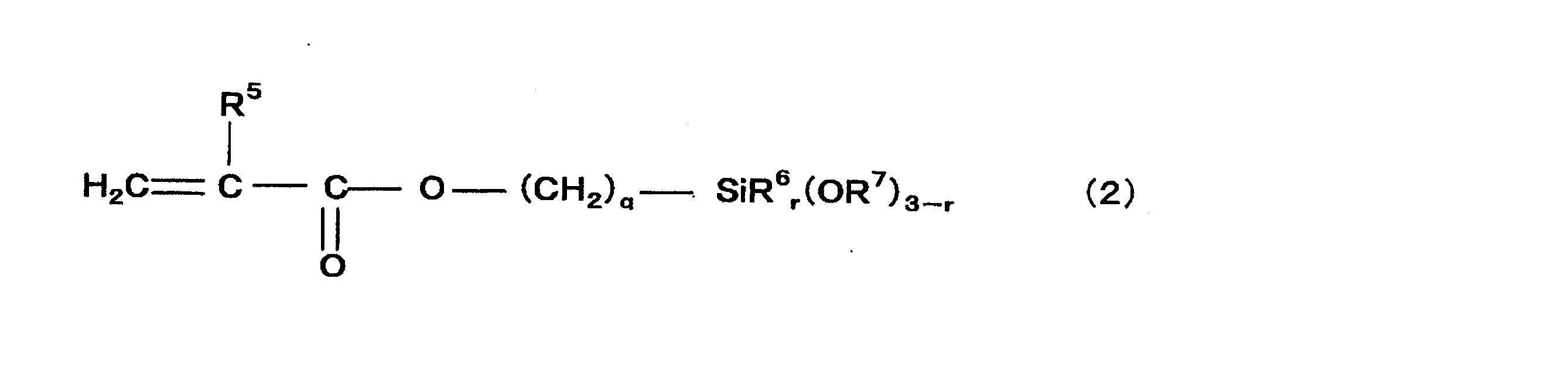
(式(2)中、R5は水素原子又はメチル基を表し、R6は炭素数1~3のアルキル基又はフェニル基を表し、R7は水素原子又は炭素数1~10の炭化水素基を表し、qは1~6の整数であり、rは0~2の整数である。)
硬化性組成物の粘度の低減、保存安定性の点から、好ましいR6はメチル基であり、好ましいR7はメチル基であり、好ましいqは3であり、好ましいrは0である。
シラン化合物(E)は硬化性組成物の粘度を低減させ、且つ後述するウレタン化合物(B)と反応することによって、シリカ微粒子(A)の硬化性組成物中における分散安定性を向上させるため、及び硬化性組成物を硬化させる際の硬化収縮を低減し、かつ硬化物に成形加工性を付与するために用いられるものである。つまり、シラン化合物(E)でシリカ微粒子(A)を表面処理しない場合には、硬化性組成物の粘度が高くなるとともに、硬化時の硬化収縮が大きくなり、硬化物が脆くなり、硬化物にクラックが発生したりするので好ましくない。
シラン化合物(E)は硬化性組成物の粘度を低減させ、且つ後述するウレタン化合物(B)と反応することによって、シリカ微粒子(A)の硬化性組成物中における分散安定性を向上させるため、及び硬化性組成物を硬化させる際の硬化収縮を低減し、かつ硬化物に成形加工性を付与するために用いられるものである。つまり、シラン化合物(E)でシリカ微粒子(A)を表面処理しない場合には、硬化性組成物の粘度が高くなるとともに、硬化時の硬化収縮が大きくなり、硬化物が脆くなり、硬化物にクラックが発生したりするので好ましくない。
シラン化合物(E)としては、例えば、γ-アクリロキシプロピルジメチルメトキシシラン、γ-アクリロキシプロピルメチルジメトキシシラン、γ-アクリロキシプロピルジエチルメトキシシラン、γ-アクリロキシプロピルエチルジメトキシシラン、γ-アクリロキシプロピルトリメトキシシラン、γ-アクリロキシプロピルジメチルエトキシシラン、γ-アクリロキシプロピルメチルジエトキシシラン、γ-アクリロキシプロピルジエチルエトキシシラン、γ-アクリロキシプロピルエチルジエトキシシラン、γ-アクリロキシプロピルトリエトキシシラン、γ-メタクリロキシプロピルジメチルメトキシシラン、γ-メタクリロキシプロピルメチルジメトキシシラン、γ-メタクリロキシプロピルジエチルメトキシシラン、γ-メタクリロキシプロピルエチルジメトキシシラン、γ-メタクリロキシプロピルトリメトキシシラン、γ-メタクリロキシプロピルジメチルエトキシシラン、γ-メタクリロキシプロピルメチルジエトキシシラン、γ-メタクリロキシプロピルジエチルエトキシシラン、γ-メタクリロキシプロピルエチルジエトキシシラン、γ-メタクリロキシプロピルトリエトキシシラン等が挙げられる。
シリカ微粒子(A)の硬化性組成物中における凝集防止、硬化性組成物の粘度の低減および保存安定性向上の点からは、γ-アクリロキシプロピルジメチルメトキシシラン、γ-アクリロキシプロピルメチルジメトキシシラン、γ-メタクリロキシプロピルジメチルメトキシシラン、γ-メタクリロキシプロピルメチルジメトキシシラン、γ-アクリロキシプロピルトリメトキシシラン、γ-メタクリロキシプロピルトリメトキシシランが好ましく、より好ましくは、γ-アクリロキシプロピルトリメトキシシランである。また、これらは、2種以上を併用して用いることができる。
また、このようなシラン化合物(E)は公知の方法で製造することができ、また市販されている。
シリカ微粒子(A)を表面処理する際のシラン化合物(E)の使用量は、シリカ微粒子A)100質量部に対して通常10~50質量部、好ましくは20~40質量部、より好ましくは24~36質量部である。シラン化合物(E)の使用量が10質量部未満であると、硬化性組成物の粘度が高くなり、シリカ微粒子(A)の硬化性組成物中への分散性が悪化してゲル化を生じる可能性がある。また、50質量部を超えると、シリカ微粒子(A)の凝集を引き起こすことがある。なお、シリカ微粒子(A)として有機溶媒に分散したシリカ微粒子を使用する場合は、前記シリカ微粒子(A)の質量は、有機溶媒に分散したシリカ微粒子そのもののみの質量を指す。また、シリカ微粒子(A)の表面処理については後述する。
シリカ微粒子(A)を表面処理する際のシラン化合物(E)の使用量は、シリカ微粒子A)100質量部に対して通常10~50質量部、好ましくは20~40質量部、より好ましくは24~36質量部である。シラン化合物(E)の使用量が10質量部未満であると、硬化性組成物の粘度が高くなり、シリカ微粒子(A)の硬化性組成物中への分散性が悪化してゲル化を生じる可能性がある。また、50質量部を超えると、シリカ微粒子(A)の凝集を引き起こすことがある。なお、シリカ微粒子(A)として有機溶媒に分散したシリカ微粒子を使用する場合は、前記シリカ微粒子(A)の質量は、有機溶媒に分散したシリカ微粒子そのもののみの質量を指す。また、シリカ微粒子(A)の表面処理については後述する。
硬化性組成物中にアクリレート(後述するウレタン化合物(B)および反応性アクリレート(C))が多く含まれる場合には、前記シラン化合物(E)として、アクリル基を有する、つまりR1が水素原子である一般式(1)で表されるシラン化合物、硬化性組成物中にメタクリレート(後述するウレタン化合物(B)およびメタクリレート(C))が多く含まれる場合は、前記シラン化合物(E)として、メタクリル基を含有する、つまりR1がメチル基である一般式(1)で表されるシラン化合物を用いることが好ましい。そのような場合には、本発明の硬化性組成物を硬化させる際に硬化反応が起こりやすい。
<(B)ウレタン化合物>
本発明で使用される(B)ウレタン化合物(以下、単に「(B)ウレタン化合物」ともいう。)は下記一般式(1)で示され、分子中に重合性不飽和結合を2個以上含有する。

上記一般式(1)中、R1は直鎖もしくは分岐を有する炭素数1~12の2価の脂肪族基、脂環基を有する炭素数3~12の2価の有機基、芳香環を有し炭素数6~30の2価の有機基または[-(CH2)a-O-(CH2)b-]cである(aおよびbはそれぞれ独立に1~10の整数、cは1~5の整数を表す。)。R1は後述する本発明の硬化性組成物の硬化性の観点と、該硬化性組成物を硬化して得られる硬化物(以下、単に「硬化物」ともいう。)の硬度とカール性とのバランスの観点から炭素数1~6の2価の脂肪族基または[-(CH2) a-O-(CH2)b-]c(aおよびbはそれぞれ独立に1~5の整数、cは1~3の整数
を表す。)であることが好ましく、炭素数2~4の2価の脂肪族基または[-(CH2)a-O-(CH2)b-]c(aおよびbはそれぞれ独立に2~4の整数、cは1または2を表す。)であることがより好ましく、炭素数2もしくは3の2価の脂肪族基または-(CH2)2-O-(CH2)2-であることがさらに好ましい。
本発明で使用される(B)ウレタン化合物(以下、単に「(B)ウレタン化合物」ともいう。)は下記一般式(1)で示され、分子中に重合性不飽和結合を2個以上含有する。
を表す。)であることが好ましく、炭素数2~4の2価の脂肪族基または[-(CH2)a-O-(CH2)b-]c(aおよびbはそれぞれ独立に2~4の整数、cは1または2を表す。)であることがより好ましく、炭素数2もしくは3の2価の脂肪族基または-(CH2)2-O-(CH2)2-であることがさらに好ましい。
上記一般式(1)中、R2は、直鎖もしくは分岐を有する炭素数1~10の2価の脂肪族基、脂環基を有する炭素数3~10の2価の有機基、芳香環を有する炭素数6~30の2価の有機基または[-(CH2)d-O-(CH2)e-]fであり(但しdおよびeはそれぞれ独立に1~10の整数、fは1~5の整数を表す)。R2は後述する本発明の硬化性組成物の硬化性の観点と、該硬化性組成物を硬化して得られる硬化物の硬度およびカール性とのバランスの観点から、炭素数1~6の2価の脂肪族基または芳香環を有する炭素数6~30の2価の有機基または[-(CH2)d-O-(CH2)e-]f(dおよびeはそれぞれ独立に1~5
の整数、fは1~3の整数を表す。)であることが好ましく、炭素数2~4の2価の脂肪族基、ベンゼン環を有する炭素数6~30の2価の有機基または[-(CH2)d-O-(CH2)e-]f(dおよびeはそれぞれ独立に2~4の整数、fは1または2を表す。)であることがより好ましく、炭素数2もしくは3の2価の脂肪族基または-(CH2)2-O-(CH2)2-であることがさらに好ましい。
の整数、fは1~3の整数を表す。)であることが好ましく、炭素数2~4の2価の脂肪族基、ベンゼン環を有する炭素数6~30の2価の有機基または[-(CH2)d-O-(CH2)e-]f(dおよびeはそれぞれ独立に2~4の整数、fは1または2を表す。)であることがより好ましく、炭素数2もしくは3の2価の脂肪族基または-(CH2)2-O-(CH2)2-であることがさらに好ましい。
上記式(1)中、R3およびR4はそれぞれ独立に水素原子またはメチル基である。低露光量で硬化するという硬化性の観点からは、水素原子であることが好ましい。
硬化性組成物に(B)ウレタン化合物を用いることで、表面硬度、透明性およびカール性のバランスに優れた硬化物が得られる。すなわち、本発明の硬化物からなる種々の製品について高い品質が達成される。
硬化性組成物に(B)ウレタン化合物を用いることで、表面硬度、透明性およびカール性のバランスに優れた硬化物が得られる。すなわち、本発明の硬化物からなる種々の製品について高い品質が達成される。
本発明の硬化性組成物100質量部のうち、(B)ウレタン化合物の含量は、好ましくは10~99質量部、より好ましくは20~99質量部、さらに好ましくは30~99質量部である。(B)ウレタン化合物の含量が前記範囲内にあることにより、硬化性、鉛筆硬度、耐擦傷性、カール性、強度と柔軟性のバランスに優れた樹脂を得ることができる。
本発明で使用される上記一般式(1)で示されるウレタン化合物は、下記一般式(3)で示される重合性不飽和基含有アルコール化合物(以下「化合物(1)」ともいう。)と、下記一般式(4)で示される重合性不飽和基含有イソシアネート化合物(以下「化合物(2)」ともいう。)とを接触させて合成することができる。


上記化合物(1)としては、例えば、2-ヒドロキシエチル(メタ)アクリレート、2-ヒドロキシプロピル(メタ)アクリレート、3-ヒドロキシプロピル(メタ)アクリレート、4-ヒドロキシブチル(メタ)アクリレート等が挙げられる。これらは1種単独でまたは2種類以上を組み合わせて使用することができる。好ましくは2-ヒドロキシエチル(メタ)アクリレートである。一般的に、R3が水素原子である場合、すなわち化合物(1)がアクリレート構造を有する場合のほうが、R3がメチル基である場合、すなわち化合物(1)がメタクリレート構造を有する場合よりも、得られるウレタン化合物を含有する硬化性組成物の硬化性が優れている傾向がある。なお、本願明細書において、「(メタ)アクリレート」の記載はメタクリレートおよび/またはアクリレートを意味する。
一般式(4)で示される分子内に不飽和基を1つ以上含むイソシアネート化合物のOCN-R2-のR2は、上記一般式(1)で表される化合物中のR2と同じであるが、OCN-R2-の具体例としては、下記に示す(a)~(e)などが挙げられる。

上記一般式(4)においてR4は水素原子またはメチル基であり、好ましくは水素原子である。
上記化合物(2)の好ましい具体例を次に示す。上記(a)の構造を有するものとしては、2-(メタ)アクリロイルオキシエチルイソシアネート、3-(メタ)アクリロイルオキシプロピルイソシアネート、4-(メタ)アクリロイルオキシブチルイソシアネート、5-(メタ)アクリロイルペンチルイソシアネート、6-(メタ)アクリロイルオキシヘキシルイソシアネート、2-(メタ)アクリロイルオキシプロピルイソシアネート、1,1-ビス(アクリロイルオキシメチル)エチルイソシアネート、上記(b)の構造を有するものとしては、3-イソシアナト-2-メチルプロピル(メタ)アクリレート、上記(c)の構造を有するものとしては、3-イソシアナトシクロヘキシル(メタ)アクリレート、4-イソシアナトシクロヘキシル(メタ)アクリレート、上記(d)の構造を有するものとしては、3-イソシアナトフェニル(メタ)アクリレート、4-イソシアナトフェニル(メタ)アクリレート、3,5-ジイソシアナト-2-メチルフェニル(メタ)アクリレート、上記(e)の構造を有するものとしては、2-(イソシアナトエチルオキシ)エチル(メタ)アクリレートが挙げられる。一般的に、R4が水素原子である場合、すなわち化合物(2)がアクリレート構造を有する場合のほうが、R4がメチル基である場合、すなわち化合物(2)がメタクリレート構造を有する場合よりも、得られるウレタン化合物を含有する硬化性組成物の硬化性が優れている傾向がある。
上記化合物(2)の好ましい具体例を次に示す。上記(a)の構造を有するものとしては、2-(メタ)アクリロイルオキシエチルイソシアネート、3-(メタ)アクリロイルオキシプロピルイソシアネート、4-(メタ)アクリロイルオキシブチルイソシアネート、5-(メタ)アクリロイルペンチルイソシアネート、6-(メタ)アクリロイルオキシヘキシルイソシアネート、2-(メタ)アクリロイルオキシプロピルイソシアネート、1,1-ビス(アクリロイルオキシメチル)エチルイソシアネート、上記(b)の構造を有するものとしては、3-イソシアナト-2-メチルプロピル(メタ)アクリレート、上記(c)の構造を有するものとしては、3-イソシアナトシクロヘキシル(メタ)アクリレート、4-イソシアナトシクロヘキシル(メタ)アクリレート、上記(d)の構造を有するものとしては、3-イソシアナトフェニル(メタ)アクリレート、4-イソシアナトフェニル(メタ)アクリレート、3,5-ジイソシアナト-2-メチルフェニル(メタ)アクリレート、上記(e)の構造を有するものとしては、2-(イソシアナトエチルオキシ)エチル(メタ)アクリレートが挙げられる。一般的に、R4が水素原子である場合、すなわち化合物(2)がアクリレート構造を有する場合のほうが、R4がメチル基である場合、すなわち化合物(2)がメタクリレート構造を有する場合よりも、得られるウレタン化合物を含有する硬化性組成物の硬化性が優れている傾向がある。
上記化合物(1)と化合物(2)とを反応させる際のモル比は、化合物(1):化合物
(2)=1:1~1:1.5である。
上記化合物(1)と、上記化合物(2)とを反応させる際には、ウレタン化触媒を使用することが好ましい。ウレタン化触媒を使用することにより、著しく反応を速めることができる。ウレタン化触媒の具体例としては、ジブチル錫ジラウリレート、ナフテン酸銅、ナフテン酸コバルト、ナフテン酸亜鉛、トリエチルアミン、1,4-ジアザビシクロ[2.2.2]オクタン、2,6,7-トリメチル-1,4-ジアザビシクロ[2.2.2]オクタンなどが挙げられる。
(2)=1:1~1:1.5である。
上記化合物(1)と、上記化合物(2)とを反応させる際には、ウレタン化触媒を使用することが好ましい。ウレタン化触媒を使用することにより、著しく反応を速めることができる。ウレタン化触媒の具体例としては、ジブチル錫ジラウリレート、ナフテン酸銅、ナフテン酸コバルト、ナフテン酸亜鉛、トリエチルアミン、1,4-ジアザビシクロ[2.2.2]オクタン、2,6,7-トリメチル-1,4-ジアザビシクロ[2.2.2]オクタンなどが挙げられる。
これらのウレタン化触媒は1種単独で用いてもよく、2種以上を組み合わせて用いてもよい。ウレタン化触媒の添加量は、化合物(2)100質量部に対して0.01~5質量部が好ましく、より好ましくは0.1~1質量部である。添加量が0.01質量部未満では反応性が低下する場合がある。一方、添加量が5質量部を超えると反応時に副反応が起きる可能性がある。
上記化合物(1)と化合物(2)との反応における反応温度は、好ましくは-10~100℃、より好ましくは0~60℃である。さらに好ましくは10~30℃である。
上記の反応はBHT(2,6-ジ-tert-ブチル-4-メチルフェノール)含有ヘキサン中で行うことができる。BHT含有ヘキサンは反応終了後にそのまま洗浄溶剤として使用することができるので、上記の反応を行う際の環境への負荷を低減させることができる。この場合のBHT含有ヘキサン中のBHTの含有量は、1~1000ppm、好ましくは50~500ppm、さらに好ましくは100~400ppmである。
上記の反応はBHT(2,6-ジ-tert-ブチル-4-メチルフェノール)含有ヘキサン中で行うことができる。BHT含有ヘキサンは反応終了後にそのまま洗浄溶剤として使用することができるので、上記の反応を行う際の環境への負荷を低減させることができる。この場合のBHT含有ヘキサン中のBHTの含有量は、1~1000ppm、好ましくは50~500ppm、さらに好ましくは100~400ppmである。
上記の量比、温度条件にて反応を行うことで副反応が抑えられ良好な収率、純度で(B)ウレタン化合物を得ることができる。また、室温付近で反応を行うことができるので(B)ウレタン化合物同士の重合の可能性を低減することができる。
<(C)(メタ)アクリレート>
硬化性組成物に用いられるエチレン性不飽和基を有し且つ脂環式構造を有する(メタ)アクリレート(C)は、硬化時の収縮を低減する効果があるため、造形時に型への形状追随性が向上する。たとえば、シクロヘキシル(メタ)アクリレート、4-ブチルシクロヘキシル(メタ)アクリレート、ジシクロペンタニル(メタ)アクリレート、ジシクロペンテニル(メタ)アクリレート、ジシクロペンタジエニル(メタ)アクリレート、ボルニル(メタ)アクリレート、イソボルニル(メタ)アクリレート、トリシクロデカニル(メタ)アクリレート、アダマンチル(メタ)アクリレート、ジシクロペンタニルジ(メタ)ア
クリレート、トリシクロデカンジメタノールジアクリレート、アダマンチルジ(メタ)アクリレートなどのシクロアルキル(メタ)アクリレート類が挙げられる。
<(C)(メタ)アクリレート>
硬化性組成物に用いられるエチレン性不飽和基を有し且つ脂環式構造を有する(メタ)アクリレート(C)は、硬化時の収縮を低減する効果があるため、造形時に型への形状追随性が向上する。たとえば、シクロヘキシル(メタ)アクリレート、4-ブチルシクロヘキシル(メタ)アクリレート、ジシクロペンタニル(メタ)アクリレート、ジシクロペンテニル(メタ)アクリレート、ジシクロペンタジエニル(メタ)アクリレート、ボルニル(メタ)アクリレート、イソボルニル(メタ)アクリレート、トリシクロデカニル(メタ)アクリレート、アダマンチル(メタ)アクリレート、ジシクロペンタニルジ(メタ)ア
クリレート、トリシクロデカンジメタノールジアクリレート、アダマンチルジ(メタ)アクリレートなどのシクロアルキル(メタ)アクリレート類が挙げられる。
上記の例示した(メタ)アクリレートの中でも、金型への形状追随性の観点から、2つのエチレン性不飽和基を有する(メタ)アクリレートが好ましく、ジシクロペンタニルジ(メタ)アクリレートが最も好ましい。
なお、脂環式構造とは、炭素原子が環状に結合した構造のうち、芳香環構造を除くものである。
硬化性組成物に用いられる(メタ)アクリレート(C)の配合量は、表面処理前のシリカ微粒子(A)100質量部に対して、5~400質量部であることが好ましく、より好ましくは10~200質量部であり、さらに好ましくは20~100質量部である。配合量が5質量部未満では、金型への形状追随性が低下する。配合量が400質量部を超えると、基板への密着性が低下することがある。なお、シリカ微粒子(A)として有機溶媒に分散したシリカ微粒子を使用する場合は、前記シリカ微粒子(A)の質量は、有機溶媒に分散したシリカ微粒子そのもののみの質量を指す。
硬化性組成物に用いられる(メタ)アクリレート(C)の配合量は、表面処理前のシリカ微粒子(A)100質量部に対して、5~400質量部であることが好ましく、より好ましくは10~200質量部であり、さらに好ましくは20~100質量部である。配合量が5質量部未満では、金型への形状追随性が低下する。配合量が400質量部を超えると、基板への密着性が低下することがある。なお、シリカ微粒子(A)として有機溶媒に分散したシリカ微粒子を使用する場合は、前記シリカ微粒子(A)の質量は、有機溶媒に分散したシリカ微粒子そのもののみの質量を指す。
<(D)重合開始剤>
硬化性組成物に用いられる重合開始剤(D)としては、ラジカルを発生する光重合開始剤及び熱重合開始剤が挙げられる。
硬化性組成物に用いられる重合開始剤(D)としては、ラジカルを発生する光重合開始剤及び熱重合開始剤が挙げられる。
前記光重合開始剤としては、例えばベンゾフェノン、ベンゾインメチルエーテル、ベンゾインプロピルエーテル、ジエトキシアセトフェノン、1-ヒドロキシ-フェニルフェニルケトン、2,6-ジメチルベンゾイルジフェニルホスフィンオキシド、2,4,6-トリメチルベンゾイルジフェニルホスフィンオキシドおよびジフェニル-(2,4,6-トリメチルベンゾイル)フォスフィンオキシドが挙げられる。これらの光重合開始剤は2種以上を併用してもよい。
光重合開始剤の硬化性組成物中における含有量は、硬化性組成物を適度に硬化させる量であればよく、硬化性組成物100質量部に対して、0.01~10質量部であることが好ましく、より好ましくは0.02~5質量部であり、さらに好ましくは0.1~2質量部である。光重合開始剤の添加量が多すぎると、硬化性組成物の保存安定性が低下したり、着色したり、架橋して硬化物を得る際の架橋が急激に進行し硬化時の割れ等の問題が発生する場合がある。また、光重合開始剤の添加量が少なすぎると硬化性組成物を十分に硬化させることができないことがある。
前記熱重合開始剤としては、ベンゾイルパーオキシド、ジイソプロピルパーオキシカーボネート、t-ブチルパーオキシ(2-エチルヘキサノエート)等が挙げられる。
熱重合開始剤の硬化性組成物中における含有量は、硬化性組成物100質量部に対して、2質量部以下であることが好ましく、0.1~2質量部であることがより好ましい。
熱重合開始剤の硬化性組成物中における含有量は、硬化性組成物100質量部に対して、2質量部以下であることが好ましく、0.1~2質量部であることがより好ましい。
また、本発明に用いられる硬化性組成物は、必要に応じて、組成物の粘度及び硬化物の透明性、耐熱性等の特性を損なわない範囲で、レベリング剤、酸化防止剤、紫外線吸収剤、溶剤、顔料、他の無機フィラー等の充填剤、反応性希釈剤、その他改質剤等を含んでいてもよい。
レベリング剤としては、例えば、ポリエーテル変性ジメチルポリシロキサン共重合物、ポリエステル変性ジメチルポリシロキサン共重合物、ポリエーテル変性メチルアルキルポリシロキサン共重合物、アラルキル変性メチルアルキルポリシロキサン共重合物、ポリエーテル変性メチルアルキルポリシロキサン共重合物等が挙げられる。
充填剤または顔料としては、炭酸カルシウム、タルク、マイカ、クレー、アエロジル(登録商標)等、硫酸バリウム、水酸化アルミニウム、ステアリン酸亜鉛、亜鉛華、ベンガラ、アゾ顔料等が挙げられる。
このような各種成分を含有する本発明の硬化性組成物の、コーンプレート式粘度計DV-IIIULTRA(BROOKFIELD社製)、25℃、スピンドルNo.CP-41で測定した粘度は、通常100~5000mPa・sであり、溶剤を含有していなくとも低粘度であり、良好なハンドリング性を有する。このことは、上述のシリカ微粒子(A)の表面処理による、シリカ微粒子(A)のウレタン化合物(B)および(メタ)アクリレート(C)との高い相溶性、ウレタン化合物(B)および(メタ)アクリレート(C)中におけるシリカ微粒子(A)の高い分散安定性に起因する。
<硬化性組成物の製造方法>
本発明本発明に用いられる硬化性組成物は、例えば、有機溶媒に分散したコロイダルシリカ(シリカ微粒子(A))をシラン化合物(E)で表面処理する工程(工程1)、表面処理したシリカ微粒子(A)にウレタン化合物(B)および(メタ)アクリレート(C)を添加し、均一混合する工程(工程2)、工程2で得られたシリカ微粒子(A)とウレタン化合物(B)および(メタ)アクリレート(C)との均一混合液から有機溶媒及び水を留去・脱溶媒する工程(工程3)、工程3で留去・脱溶媒された組成物に重合開始剤(D)を添加、均一混合して硬化性組成物とする工程(工程4)を順次行うことにより製造することができる。以下各工程について説明する。
本発明本発明に用いられる硬化性組成物は、例えば、有機溶媒に分散したコロイダルシリカ(シリカ微粒子(A))をシラン化合物(E)で表面処理する工程(工程1)、表面処理したシリカ微粒子(A)にウレタン化合物(B)および(メタ)アクリレート(C)を添加し、均一混合する工程(工程2)、工程2で得られたシリカ微粒子(A)とウレタン化合物(B)および(メタ)アクリレート(C)との均一混合液から有機溶媒及び水を留去・脱溶媒する工程(工程3)、工程3で留去・脱溶媒された組成物に重合開始剤(D)を添加、均一混合して硬化性組成物とする工程(工程4)を順次行うことにより製造することができる。以下各工程について説明する。
(工程1)
工程1では、シリカ微粒子(A)をシラン化合物(E)で表面処理する。表面処理は、シリカ微粒子(A)を反応器に入れ、攪拌しながら、シラン化合物(E)を添加、攪拌混合し、さらに該シラン化合物の加水分解を行うのに必要な水と触媒を添加、攪拌しながら、該シラン化合物を加水分解し、シリカ微粒子(A)表面にて縮重合させることにより行う。なお、前記シリカ微粒子(A)としては、有機溶媒に分散したシリカ微粒子を用いることが好ましいことは、前述のとおりである。
工程1では、シリカ微粒子(A)をシラン化合物(E)で表面処理する。表面処理は、シリカ微粒子(A)を反応器に入れ、攪拌しながら、シラン化合物(E)を添加、攪拌混合し、さらに該シラン化合物の加水分解を行うのに必要な水と触媒を添加、攪拌しながら、該シラン化合物を加水分解し、シリカ微粒子(A)表面にて縮重合させることにより行う。なお、前記シリカ微粒子(A)としては、有機溶媒に分散したシリカ微粒子を用いることが好ましいことは、前述のとおりである。
なお、前記シラン化合物の加水分解による消失を、ガスクロマトグラフィーにより確認することができる。ガスクロマトグラフィー(アジレント(株)製 型式6850)にて、無極性カラムDB-1(J&W社製)を使用し、温度50~300℃、昇温速度10℃/min、キャリアガスとしてHeを使用し、流量1.2cc/min、水素炎イオン化検出器にて内部標準法でシラン化合物の残存量を測定することができるため、シラン化合物の加水分解による消失を確認することができる。
なお、前述のようにシリカ微粒子(A)を表面処理する際のシラン化合物(E)の使用量は、シリカ微粒子(A)100質量部に対して通常10~50質量部、好ましくは20~40質量部、より好ましくは24~36質量部である。
加水分解反応を行うのに必要な水の量の下限値は、シラン化合物(E)に結合したアルコキシ基およびヒドロキシ基のモル数の合計の1倍、上限値は10倍である。水の量が過度に少ないと、加水分解速度が極端に遅くなり経済性に欠けたり、表面処理が充分進行しないおそれがある。逆に水の量が過度に多いと、シリカ微粒子(A)がゲルを形成するおそれがある。
加水分解反応を行う際には、通常、加水分解反応用の触媒が使用される。このような触媒の具体例としては、例えば、塩酸、酢酸、硫酸、リン酸等の無機酸;
蟻酸、プロピオン酸、シュウ酸、パラトルエンスルホン酸、安息香酸、フタル酸、マレイン酸等の有機酸;
水酸化カリウム、水酸化ナトリウム、水酸化カルシウム、アンモニア等のアルカリ触媒;有機金属;
金属アルコキシド;
ジブチルスズジラウレート、ジブチルスズジオクチレート、ジブチルスズジアセテート等の有機スズ化合物;
アルミニウムトリス(アセチルアセトネート)、チタニウムテトラキス(アセチルアセトネート)、チタニウムビス(ブトキシ)ビス(アセチルアセトネート)、チタニウムビス(イソプロポキシ)ビス(アセチルアセトネート)、ジルコニウムビス(ブトキシ)ビス(アセチルアセトネート)、ジルコニウムビス(イソプロポキシ)ビス(アセチルアセトネート)等の金属キレート化合物;
ホウ素ブトキシド、ホウ酸等のホウ素化合物;
等が挙げられる。
蟻酸、プロピオン酸、シュウ酸、パラトルエンスルホン酸、安息香酸、フタル酸、マレイン酸等の有機酸;
水酸化カリウム、水酸化ナトリウム、水酸化カルシウム、アンモニア等のアルカリ触媒;有機金属;
金属アルコキシド;
ジブチルスズジラウレート、ジブチルスズジオクチレート、ジブチルスズジアセテート等の有機スズ化合物;
アルミニウムトリス(アセチルアセトネート)、チタニウムテトラキス(アセチルアセトネート)、チタニウムビス(ブトキシ)ビス(アセチルアセトネート)、チタニウムビス(イソプロポキシ)ビス(アセチルアセトネート)、ジルコニウムビス(ブトキシ)ビス(アセチルアセトネート)、ジルコニウムビス(イソプロポキシ)ビス(アセチルアセトネート)等の金属キレート化合物;
ホウ素ブトキシド、ホウ酸等のホウ素化合物;
等が挙げられる。
これらの中でも、水への溶解性、充分な加水分解速度が得られる点から、塩酸、酢酸、マレイン酸、ホウ素化合物が好ましい。これらの触媒は、1種又は2種以上を組み合わせて用いることができる。
工程1において、シラン化合物(E)の加水分解反応を行う際には、非水溶性触媒を用いてもよいが、水溶性触媒を使用することが好ましい。加水分解反応用の水溶性触媒を使用する場合は、水溶性触媒を適当量の水に溶解し、反応系に添加すると、触媒を均一に分散させることができるので好ましい。
加水分解反応に使用する触媒の添加量は、特に限定されないが、通常シリカ微粒子(a
)100質量部に対して、0.1~10質量部、好ましくは0.5~5質量部である。なお、シリカ微粒子(A)として有機溶媒に分散したシリカ微粒子を使用する場合は、前記シリカ微粒子(A)の質量は、有機溶媒に分散したシリカ微粒子そのもののみの質量を指す。
)100質量部に対して、0.1~10質量部、好ましくは0.5~5質量部である。なお、シリカ微粒子(A)として有機溶媒に分散したシリカ微粒子を使用する場合は、前記シリカ微粒子(A)の質量は、有機溶媒に分散したシリカ微粒子そのもののみの質量を指す。
加水分解反応の反応温度は特に限定されないが、通常、10~80℃の範囲であり、好ましくは20~50℃の範囲である。反応温度が過度に低いと、加水分解速度が極端に遅くなり経済性に欠けたり、表面処理が充分進行しなかったりするおそれがある。反応温度が過度に高いと、ゲル化反応が起こりやすくなる傾向がある。
また、加水分解反応を行うための反応時間は特に限定されないが、通常10分間~48時間、好ましくは30分間~24時間の範囲である。
(工程2)
工程2において、表面処理したシリカ微粒子(A)とウレタン化合物(B)および(メタ)アクリレート(C)とを混合する方法は、特に制限は無いが、たとえば、室温または加熱条件下でミキサー、ボールミル、3本ロールなどの混合機により混合する方法や、工程1を行った反応器の中で連続的に攪拌しながらウレタン化合物(B)および(メタ)アクリレート(C)を添加、混合する方法が挙げられる。
工程2において、表面処理したシリカ微粒子(A)とウレタン化合物(B)および(メタ)アクリレート(C)とを混合する方法は、特に制限は無いが、たとえば、室温または加熱条件下でミキサー、ボールミル、3本ロールなどの混合機により混合する方法や、工程1を行った反応器の中で連続的に攪拌しながらウレタン化合物(B)および(メタ)アクリレート(C)を添加、混合する方法が挙げられる。
(工程3)
工程3において、シリカ微粒子(A)とウレタン化合物(B)および(メタ)アクリレート(C)との均一混合液から有機溶媒及び水を留去・脱溶媒(以下これらをまとめて脱溶媒という)するには、減圧状態で加熱することが好ましい。
工程3において、シリカ微粒子(A)とウレタン化合物(B)および(メタ)アクリレート(C)との均一混合液から有機溶媒及び水を留去・脱溶媒(以下これらをまとめて脱溶媒という)するには、減圧状態で加熱することが好ましい。
温度は、20~100℃に保つことが好ましく、凝集ゲル化防止と脱溶媒スピードとのバランスで、より好ましくは30~70℃、さらに好ましくは30~50℃である。温度を上げすぎると、硬化性組成物の流動性が極端に低下したり、硬化性組成物がゲル状になってしまったりすることがある。
減圧する際の真空度は、通常10~4000kPaであり、脱溶媒スピードと凝集ゲル化防止とのバランスを図る上で、さらに好ましくは10~1000kPa、最も好ましくは、10~500kPaである。真空度の値が大きすぎると、脱溶媒スピードが極端に遅くなり経済性にかける。
脱溶媒後の組成物は、実質的に溶媒を含まないことが好ましい。ここでいう実質的とは、硬化性組成物を用いて実際に硬化物を得る際に、再度、脱溶媒する工程を経る必要がないことを意味しており、具体的には、硬化性組成物中の有機溶媒及び水の残存量として、1質量%以下が好ましく、好ましくは0.5質量%以下、更に好ましくは0.1質量%以下であることを意味する。
工程3においては、脱溶媒する前に、脱溶媒後の組成物100質量部に対して0.1質量部以下の重合禁止剤を添加してもよい。重合禁止剤は脱溶媒過程中や脱溶媒後の組成物及び硬化性組成物の保存中に組成物の含有成分が重合反応を起こすのを防止するために用いられる。重合禁止剤としては、例えば、ハイドロキノン、ハイドロキノンモノメチルエーテル、ベンゾキノン、p-t-ブチルカテコール、2,6-ジ-t-ブチル-4-メチルフェノール等が挙げられる。これらは1種又は2種以上を組み合わせて用いることができる。
工程3は、工程2を経たシリカ微粒子(A)とウレタン化合物(B)および(メタ)アクリレート(C)との均一混合液を専用の装置に移して行うこともできるし、工程2を、工程1を実施した反応器で行ったのであれば、工程2に引き続いて該反応器中で行うことができる。
(工程4)
工程4において、工程3で脱溶媒された組成物に重合開始剤(D)を添加、均一混合する方法は、特に制限は無いが、たとえば、室温でミキサー、ボールミル、3本ロールなどの混合機により混合する方法や、工程1~3を行った反応器の中で連続的に攪拌しながら重合開始剤(D)を添加、混合する方法が挙げられる。
工程4において、工程3で脱溶媒された組成物に重合開始剤(D)を添加、均一混合する方法は、特に制限は無いが、たとえば、室温でミキサー、ボールミル、3本ロールなどの混合機により混合する方法や、工程1~3を行った反応器の中で連続的に攪拌しながら重合開始剤(D)を添加、混合する方法が挙げられる。
さらに、このような重合開始剤(D)の添加、混合を行って得られた硬化性組成物に対して、必要に応じて濾過を行ってもよい。この濾過は、硬化性組成物中のゴミ等の外来の異物除去を目的として行う。濾過方法には、特に制限は無いが、加圧濾過孔径1.0μmのメンブレンタイプ、カートリッジタイプ等のフィルターを使用し、加圧濾過する方法が好ましい。
以上の各工程を経ることにより、本発明に用いられる硬化性組成物を製造することができる。この硬化性組成物は、その構成成分であるシリカ微粒子(A)が特定のシラン化合物で処理されているため、溶剤を含有していなくとも粘度が低く、ハンドリング性が良好である。
以上の各工程を経ることにより、本発明に用いられる硬化性組成物を製造することができる。この硬化性組成物は、その構成成分であるシリカ微粒子(A)が特定のシラン化合物で処理されているため、溶剤を含有していなくとも粘度が低く、ハンドリング性が良好である。
[硬化物]
本発明に用いられる硬化性組成物は、硬化することにより、光学レンズ、光学レンズ成形用型、光ディスク基板、液晶表示素子用プラスチック基板、カラーフィルター用基板、有機EL表示素子用プラスチック基板、太陽電池基板、タッチパネル、光学素子、光導波路、LED封止材等の部材として用いることができる硬化物となる。
中でも硬化収縮率が小さいことから各種成形用の型に使用でき、特にレンズアレイ等の光学部品を成形するために用いられる型として好適に用いることができる硬化物となる。
本発明に用いられる硬化性組成物は、硬化することにより、光学レンズ、光学レンズ成形用型、光ディスク基板、液晶表示素子用プラスチック基板、カラーフィルター用基板、有機EL表示素子用プラスチック基板、太陽電池基板、タッチパネル、光学素子、光導波路、LED封止材等の部材として用いることができる硬化物となる。
中でも硬化収縮率が小さいことから各種成形用の型に使用でき、特にレンズアレイ等の光学部品を成形するために用いられる型として好適に用いることができる硬化物となる。
<硬化物の製造方法>
本発明に用いられる硬化性組成物を硬化させることにより、硬化物が得られる。硬化の方法としては、活性エネルギー線の照射によりウレタン化合物(B)および(メタ)アクリレート(C)のエチレン性不飽和基を架橋させる方法、熱をかけてエチレン性不飽和基を熱重合させる方法等があり、これらを併用することもできる。
本発明に用いられる硬化性組成物を硬化させることにより、硬化物が得られる。硬化の方法としては、活性エネルギー線の照射によりウレタン化合物(B)および(メタ)アクリレート(C)のエチレン性不飽和基を架橋させる方法、熱をかけてエチレン性不飽和基を熱重合させる方法等があり、これらを併用することもできる。
硬化性組成物を紫外線等の活性エネルギー線により硬化させる場合は、上記の工程4において、硬化性組成物中に光重合開始剤を含有させる。
硬化性組成物に熱をかけて硬化させる場合は、上記の工程4において、硬化性組成物中に熱重合開始剤を含有させる。
硬化性組成物に熱をかけて硬化させる場合は、上記の工程4において、硬化性組成物中に熱重合開始剤を含有させる。
本発明に用いられる硬化性組成物の硬化物は、例えば、硬化性組成物をガラス板、プラスチック板、金属板、シリコンウエハ等の基材上に塗布して塗膜を形成した後、その硬化性組成物に活性エネルギー線を照射することによって、あるいは加熱することによって、得ることができる。硬化のために、活性エネルギー線の照射と加熱との両方を行ってもよい。
硬化性組成物の塗布方法としては、例えば、バーコーター、アプリケーター、ダイコーター、スピンコーター、スプレーコーター、カーテンコーター、ロールコーターなどによる塗布、スクリーン印刷などによる塗布、ディッピングなどによる塗布が挙げられる。
本発明に用いられる硬化性組成物の基材上への塗布量は特に限定されず、目的に応じて適宜調整することができる。成形性の観点からは、活性エネルギー線照射および/または加熱での硬化処理後に得られる塗膜の膜厚が、1~200μmとなる量が好ましく、5~100μmとなる量がより好ましい。
硬化のために使用される活性エネルギー線としては、電子線、または紫外から赤外の波長範囲の光が好ましい。
光源としては、例えば、紫外線であれば超高圧水銀光源またはメタルハライド光源、可視光線であればメタルハライド光源またはハロゲン光源、赤外線であればハロゲン光源が使用できるが、この他にもレーザー、LEDなどの光源が使用できる。
光源としては、例えば、紫外線であれば超高圧水銀光源またはメタルハライド光源、可視光線であればメタルハライド光源またはハロゲン光源、赤外線であればハロゲン光源が使用できるが、この他にもレーザー、LEDなどの光源が使用できる。
活性エネルギー線の照射量は、光源の種類、塗膜の膜厚などに応じて適宜設定されるが、好ましくはウレタン化合物(B)および(メタ)アクリレート(C)のエチレン性不飽和基の反応率が80%以上、より好ましくは90%以上になるように適宜設定できる。
また、活性エネルギー線を照射して硬化させた後、必要に応じて、加熱処理(アニール処理)をして硬化をさらに進行させてもよい。その際の加熱温度は、80~200℃の範囲にあることが好ましい。加熱時間は、10分~60分の範囲にあることが好ましい。
本発明に用いられる硬化性組成物の硬化のために加熱処理により熱重合させる場合は、加熱温度は、80~200℃の範囲にあることが好ましく、より好ましくは100~150℃の範囲である。加熱温度が80℃より低いと、加熱時間を長くする必要があり経済性に欠ける傾向にあり、加熱温度が200℃より高いと、エネルギーコストがかかるうえに、加熱昇温時間及び降温時間がかかるため、経済性に欠ける傾向にある。
加熱時間は、加熱温度、塗膜の膜厚などに応じて適宜設定されるが、好ましくはウレタン化合物(B)および(メタ)アクリレート(C)のエチレン性不飽和基の反応率が80%以上、より好ましくは90%以上になるように適宜設定できる。
熱重合により硬化性組成物を硬化させた後、必要に応じて、加熱処理(アニール処理)
をして硬化をさらに進行させてもよい。その際の加熱温度は、150~200℃の範囲にあることが好ましい。加熱時間は、5分~60分の範囲にあることが好ましい。
熱重合により硬化性組成物を硬化させた後、必要に応じて、加熱処理(アニール処理)
をして硬化をさらに進行させてもよい。その際の加熱温度は、150~200℃の範囲にあることが好ましい。加熱時間は、5分~60分の範囲にあることが好ましい。
<硬化物>
本発明に用いられる硬化性組成物の硬化物は、透明性、硬化性、形状追随性、基板密着性に優れることから、レンズアレイ等の光学部品を成形するために用いられる型を成形するのに好適に用いることができる。
本発明に用いられる硬化性組成物の硬化物は、透明性、硬化性、形状追随性、基板密着性に優れることから、レンズアレイ等の光学部品を成形するために用いられる型を成形するのに好適に用いることができる。
前記硬化物は透明性に優れているため、硬化膜100μm厚みでの波長400nmの光線透過率が好ましくは85%以上である。波長400nmの光線透過率が85%以下の場合は、光を利用する効率が低下するので、光硬化させる際の硬化性を損ねることがあるので好ましくない。
硬化性に乏しい場合は、空気と接触している部分が酸素阻害により硬化しないので所望の形状が得られないことが生じたり、硬化させるために、光照射エネルギーが多量に必要になったり、加熱時間が長くなったりするので生産性の観点でも好ましくないが、前記硬化物は、硬化性に優れているため、空気中で光硬化または熱硬化する際、酸素阻害を受けることなく容易に硬化物を得ることができる。
前記硬化物は、ガラス等の基板上に硬化性組成物が塗布され、その硬化性組成物に転写体が接触し、その転写体の形状にならって硬化性組成物を変形した状態で硬化化性組成物を光を照射する等によって硬化させることによって得られ、転写体に形成された転写形状が硬化物に転写される。前記硬化物は、転写体への形状追随性に優れている。ここで言う「形状追随性に優れる」とは、転写体の形状がそのまま硬化物の形状として転写され、硬化物の表面にしわやクラックが生じにくいことを意味する。
前記硬化物は、ガラス等の基板上に硬化性組成物が塗布され、その硬化性組成物に転写体が接触し、その転写体の形状にならって硬化性組成物を変形した状態で硬化性組成物を光を照射する等によって硬化させた後、転写体から離間される。この離間される際に、基板側へ密着保持されていることが必要で有るが、前記硬化物は、基板密着性に優れている。基板密着性が劣ると転写体側へ前記硬化物が持っていかれ、基板から硬化物が剥れてしまうので、たとえば光学部品を成形するために用いられる型として機能しなくなってしまうので好ましくない。
以下、本発明に用いられる硬化性組成物を実施例により詳細に説明するが、この硬化性組成物は、その要旨を越えない限り以下の例に限定されるものではない。
(合成例1)
<ウレタン化合物(B-1)>
反応容器中に2-ヒドロキシエチルアクリレート(大阪有機化学工業(株)製)100部、2,6-ジ-tert-ブチル-4-メチルフェノール(BHT、純正化学(株)製)200ppm含有ヘキサン(純正化学(株)製)142部、ジブチル錫ジラウリレート(東京化成工業(株)製)2.8部を入れて撹拌した。その後、2-アクリロイルオキシエチルイソシアネート(昭和電工(株)製、商品名カレンズ(登録商標)AOI)122部を徐々に滴下し、室温にて撹拌を行った。高速液体クロマトグラフィーで2-ヒドロキシエチルアクリレートのピークがほぼ消失したことを確認して反応を終了し、続いてBHT200ppm含有ヘキサン203部を用いて4回洗浄を行いウレタン化合物(B-1)を得た。
(合成例2)
<ウレタン化合物(B-2)>
合成例1において、2-アクリロイルオキシエチルイソシアネートにかえて2-メタクリロイルオキシエチルイソシアネート(昭和電工(株)製、商品名カレンズ(登録商標)MOI)を使用する以外は、合成例1と同様にしてウレタン化合物(B-2)を得た。
[硬化性組成物の調製]
(調製例1)
セパラブルフラスコに、イソプロピルアルコール分散型コロイダルシリカ(シリカ含量30質量%、平均粒子径10~20nm、商品名スノーテックIPA-ST;日産化学(株)製)100質量部を入れ、該セパラブルフラスコにγ-メタクリロキシプロピルトリメトキシシラン9.0質量部を加え、攪拌混合し、さらに0.1825質量%の HCl溶液2.9質量部を加え、20℃で24hr撹拌することにより、シリカ微粒子の表面処理を行った。
<ウレタン化合物(B-1)>
反応容器中に2-ヒドロキシエチルアクリレート(大阪有機化学工業(株)製)100部、2,6-ジ-tert-ブチル-4-メチルフェノール(BHT、純正化学(株)製)200ppm含有ヘキサン(純正化学(株)製)142部、ジブチル錫ジラウリレート(東京化成工業(株)製)2.8部を入れて撹拌した。その後、2-アクリロイルオキシエチルイソシアネート(昭和電工(株)製、商品名カレンズ(登録商標)AOI)122部を徐々に滴下し、室温にて撹拌を行った。高速液体クロマトグラフィーで2-ヒドロキシエチルアクリレートのピークがほぼ消失したことを確認して反応を終了し、続いてBHT200ppm含有ヘキサン203部を用いて4回洗浄を行いウレタン化合物(B-1)を得た。
(合成例2)
<ウレタン化合物(B-2)>
合成例1において、2-アクリロイルオキシエチルイソシアネートにかえて2-メタクリロイルオキシエチルイソシアネート(昭和電工(株)製、商品名カレンズ(登録商標)MOI)を使用する以外は、合成例1と同様にしてウレタン化合物(B-2)を得た。
[硬化性組成物の調製]
(調製例1)
セパラブルフラスコに、イソプロピルアルコール分散型コロイダルシリカ(シリカ含量30質量%、平均粒子径10~20nm、商品名スノーテックIPA-ST;日産化学(株)製)100質量部を入れ、該セパラブルフラスコにγ-メタクリロキシプロピルトリメトキシシラン9.0質量部を加え、攪拌混合し、さらに0.1825質量%の HCl溶液2.9質量部を加え、20℃で24hr撹拌することにより、シリカ微粒子の表面処理を行った。
なお、γ-メタクリロキシプロピルトリメトキシシランの加水分解による消失を、ガスクロマトグラフィー(アジレント(株)製 型式6850)により確認した。無極性カラムDB-1(J&W社製)を使用し、温度50~300℃、昇温速度10℃/min、キャリアガスとしてHeを使用し、流量1.2cc/min、水素炎イオン化検出器にて内部標準法で測定した。γ-メタクリロキシプロピルトリメトキシシランは、上記HCl溶液を添加後8hrで消失した。
次に、表面処理を行ったシリカ微粒子にウレタン化合物(B-1)22.0質量部とジシクロペンタジエニルジアクリレート(商品名ライトアクリレートDCP-A;共栄社化学(株)製)14.7質量部を加えて均一に混合した。その後、攪拌しながら40℃、100kPaにて減圧加熱して、揮発分を除去した。揮発分の除去量は72.0質量部であった。
この揮発分の除去により得られた母液76.6質量部に、光重合開始剤としてD1173(チバ・スペシャリティ・ケミカルズ(株)製、商品名:DAROCURE1173)0.766質量部およびMBF(チバ・スペシャリティ・ケミカルズ(株)製、メチルベンゾイルホルメート、商品名:DAROCURE MBF)1.532質量部を溶解し、メンブレンフィルター(孔径1.0μm)で加圧ろ過(圧力0.2MPa)して硬化性組成物1を得た。この硬化性組成物1の粘度は3700mPa・Sであった。
(調製例2)
調製例1において、ウレタン化合物(B-1)に代えて、ウレタン化合物(B-2)を用いた以外は、調製例1と同様にして硬化性組成物2を得た。この硬化性組成物2の粘度は3300mPa・Sであった。
調製例1において、ウレタン化合物(B-1)に代えて、ウレタン化合物(B-2)を用いた以外は、調製例1と同様にして硬化性組成物2を得た。この硬化性組成物2の粘度は3300mPa・Sであった。
(比較調製例1)
調製例1において、ウレタン化合物(B-1)に代えて、エチレンオキサイド変性トリメチロールプロパントリアクリレート(大阪有機化学(株)製、商品名ビスコート#360)を用いた以外は、調製例1と同様にし硬化性組成物3を得た。この硬化性組成物3の粘度は3000mPa・Sであった。
調製例1において、ウレタン化合物(B-1)に代えて、エチレンオキサイド変性トリメチロールプロパントリアクリレート(大阪有機化学(株)製、商品名ビスコート#360)を用いた以外は、調製例1と同様にし硬化性組成物3を得た。この硬化性組成物3の粘度は3000mPa・Sであった。
(比較調製例2)
調製例1において、ウレタン化合物(B-1)に代えて、エチルアダマンチルアクリレート(大阪有機化学(株)製、商品名EtADA)を用いた以外は、調製例1と同様にし硬化性組成物4を得た。この硬化性組成物4の粘度は4100mPa・Sであった。
調製例1において、ウレタン化合物(B-1)に代えて、エチルアダマンチルアクリレート(大阪有機化学(株)製、商品名EtADA)を用いた以外は、調製例1と同様にし硬化性組成物4を得た。この硬化性組成物4の粘度は4100mPa・Sであった。
以上の硬化性組成物の調製に用いた各成分の組成を下記表1に示す。
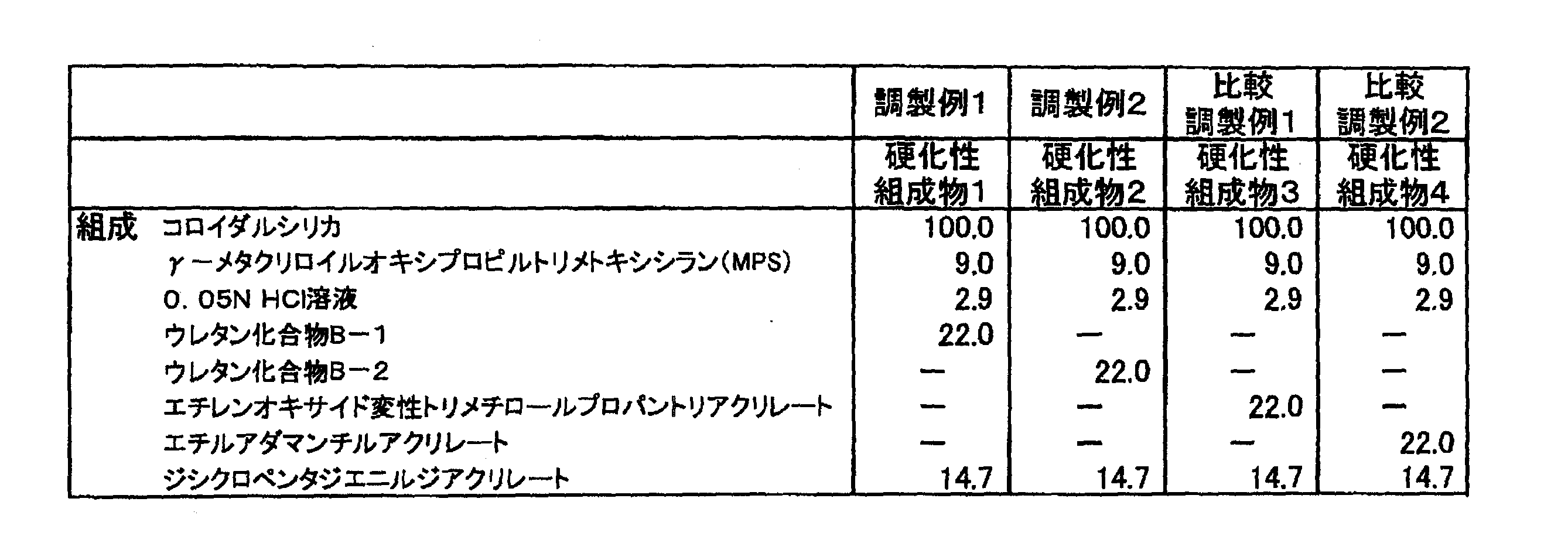
[硬化膜の調製]
<活性エネルギー線硬化>
実施例及び比較例において、硬化性組成物をそれぞれ別々のガラス基板(50mm×50mm)上に、硬化膜の厚みが100μmになるように塗布し、超高圧水銀ランプを組み込んだ露光装置で4J/cm2露光し塗膜を硬化させた。
<活性エネルギー線硬化>
実施例及び比較例において、硬化性組成物をそれぞれ別々のガラス基板(50mm×50mm)上に、硬化膜の厚みが100μmになるように塗布し、超高圧水銀ランプを組み込んだ露光装置で4J/cm2露光し塗膜を硬化させた。
[性能評価方法]
<透過率>
得られた硬化膜の波長400nmの光の透過率を、JIS-K7105に準拠し、分光光度計(日本分光(株)製、UV3100)を用いて測定した。結果を表2に示した。その透過率の値が大きいほど透明性が良好な硬化膜である。
また、得られた硬化膜の全光線透過率を、色彩濁度計(日本電色工業(株)製、COH400)を用いて測定した。結果を表2に示した。その全光線透過率の値が大きいほど透明性が良好な硬化膜である。
<透過率>
得られた硬化膜の波長400nmの光の透過率を、JIS-K7105に準拠し、分光光度計(日本分光(株)製、UV3100)を用いて測定した。結果を表2に示した。その透過率の値が大きいほど透明性が良好な硬化膜である。
また、得られた硬化膜の全光線透過率を、色彩濁度計(日本電色工業(株)製、COH400)を用いて測定した。結果を表2に示した。その全光線透過率の値が大きいほど透明性が良好な硬化膜である。
<形状追随性>
図3に示すように、ウエハW上に、注入装置を用いて上記硬化性組成物を注入し、硬化性組成物に対して、凸部90が光硬化性組成物に接触するように転写体62を接触させ、超高圧水銀ランプを組み込んだ露光装置で4J/cm2露光し硬化させた。その後、転写体62をウエハWから離間させた。上記操作を100回繰り返して100個の転写体62の形状が転写された硬化物を得た。この100個の硬化物の形状を光学顕微鏡で観察し、しわやクラックの有無を評価した。評価基準は以下の通りとし、結果を表2に示した。
A:しわ、クラックが全く生じない
B:しわ、クラックが生じない頻度が90/100以上
C:しわ、クラックが生じない頻度が50/100以上、90/100未満
D:しわ、クラックが生じない頻度が50/100未満
図3に示すように、ウエハW上に、注入装置を用いて上記硬化性組成物を注入し、硬化性組成物に対して、凸部90が光硬化性組成物に接触するように転写体62を接触させ、超高圧水銀ランプを組み込んだ露光装置で4J/cm2露光し硬化させた。その後、転写体62をウエハWから離間させた。上記操作を100回繰り返して100個の転写体62の形状が転写された硬化物を得た。この100個の硬化物の形状を光学顕微鏡で観察し、しわやクラックの有無を評価した。評価基準は以下の通りとし、結果を表2に示した。
A:しわ、クラックが全く生じない
B:しわ、クラックが生じない頻度が90/100以上
C:しわ、クラックが生じない頻度が50/100以上、90/100未満
D:しわ、クラックが生じない頻度が50/100未満
<基板密着性>
図3に示すように、ウエハW上に、注入装置を用いて上記硬化性組成物を注入し、硬化性組成物に対して、凸部90が光硬化性組成物に接触するように転写体62を接触させ、超高圧水銀ランプを組み込んだ露光装置で4J/cm2露光し硬化させた。その後、転写体62をウエハWから離間させた。上記操作を100回繰り返した。転写体62をウエハWから離間させた際に、硬化物の基板密着性が悪いと、硬化物が転写体62側にくっついてしまいウエハWからはがれてしまう。100個の硬化物中ウエハWに密着して得られた個数を基板密着性として評価した結果を表2に示した。例えば、100個中90個がウエハWに密着した場合は90/100として評価結果を表現した。
図3に示すように、ウエハW上に、注入装置を用いて上記硬化性組成物を注入し、硬化性組成物に対して、凸部90が光硬化性組成物に接触するように転写体62を接触させ、超高圧水銀ランプを組み込んだ露光装置で4J/cm2露光し硬化させた。その後、転写体62をウエハWから離間させた。上記操作を100回繰り返した。転写体62をウエハWから離間させた際に、硬化物の基板密着性が悪いと、硬化物が転写体62側にくっついてしまいウエハWからはがれてしまう。100個の硬化物中ウエハWに密着して得られた個数を基板密着性として評価した結果を表2に示した。例えば、100個中90個がウエハWに密着した場合は90/100として評価結果を表現した。
<硬化収縮率>
スピンコーター法で樹脂溶液をシリコンウェハ上に塗布した。この塗布基板を光学式膜厚計で測定した。この膜厚を初期膜厚とする。その後、窒素雰囲気下で露光し、硬化膜を作成し、その膜厚を同様の方法で測定した。この膜厚を露光後膜厚とする。硬化収縮率を以下の式により求めた。尚、測定は5箇所で行い、それらを平均した。
(初期膜厚-露光後膜厚)/初期膜厚 ×100 <%>

スピンコーター法で樹脂溶液をシリコンウェハ上に塗布した。この塗布基板を光学式膜厚計で測定した。この膜厚を初期膜厚とする。その後、窒素雰囲気下で露光し、硬化膜を作成し、その膜厚を同様の方法で測定した。この膜厚を露光後膜厚とする。硬化収縮率を以下の式により求めた。尚、測定は5箇所で行い、それらを平均した。
(初期膜厚-露光後膜厚)/初期膜厚 ×100 <%>
表2より、調製例1及び2の硬化性組成物は、形状追随性、基板密着性、透明性ともに優れることから、レンズアレイ等の光学部品を成形するために用いられる型を成形するのに好適に用いることができる。
一方、比較例調製1の硬化性組成物は、基板密着性、透明性に優れるが、形状追随性に劣り、しわ、クラックが発生することがあるため、好ましくない。
また、比較調製例2の硬化性組成物は、透明性に優れるが、形状追随性、基板密着性に劣り、基板からの剥れが生じることがあり、基板に密着したしているものにおいても、しわ、クラックが発生することがありため、好ましくない。
(実施例)
上記の硬化性組成物の調製例1および2で示した方法で作製した硬化性組成物1および2を用いて、図10、図11および図12に示した工程を行ったところ、良好なレンズアレイおよびレンズの成形に用いられる型を得ることができた。特に、レンズの成形に用いられる型の造形については、形状追随性、基板密着性ともに良好であった。
(実施例)
上記の硬化性組成物の調製例1および2で示した方法で作製した硬化性組成物1および2を用いて、図10、図11および図12に示した工程を行ったところ、良好なレンズアレイおよびレンズの成形に用いられる型を得ることができた。特に、レンズの成形に用いられる型の造形については、形状追随性、基板密着性ともに良好であった。
以上述べたように、本発明は、例えば、非球面形状からなるレンズ部を有するレンズアレイ等のレンズや、このようなレンズの成形に用いられる型等の造形物を造形する造形方法に適用することができる。
Claims (5)
- 被造形物と、転写形状が形成された転写体とを互いに接触させ、被造形物を前記転写形状にならって変形させる変形工程と、
被造形物の、少なくとも変形した部分を硬化させる硬化工程と、
被造形物と前転写体とを互いに離間させる離間工程と、
を有し、被造形物に前記転写形状を転写する転写工程を複数回繰り返す造形方法であって、前記被造形物が、重合性官能基を有するウレタン化合物と重合開始剤とを含む硬化性組成物からなる造形方法。 - 前記硬化性組成物は、
(A)シリカ微粒子と、
(B)下記一般式(1)で表されるウレタン化合物と、

R2は、直鎖もしくは分岐を有する炭素数1~10の2価の脂肪族基、脂環基を有する炭素数3~10の2価の有機基、芳香環を有する炭素数6~30の2価の有機基または[-(CH2)d-O-(CH2)e-]f(dおよびeはそれぞれ独立に1~10の整数、fは1~5の整数を表す。)であり、
R3およびR4はそれぞれ独立に水素原子またはメチル基である。)
(C)エチレン性不飽和基を有し且つ脂環式構造を有する(メタ)アクリレートと、
(D)重合開始剤と
を含み、
前記シリカ微粒子(A)が、下記一般式(2)で表されるシラン化合物(E)で表面処理されていることを特徴とする、請求項1に記載の造形方法。
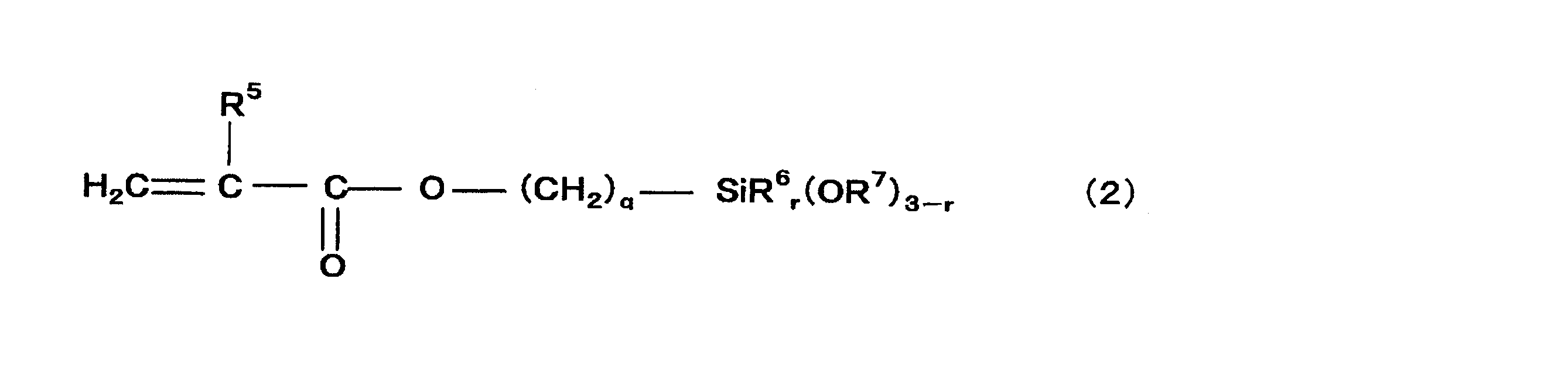
- 前記(メタ)アクリレート(C)が、2つのエチレン性不飽和基を有することを特徴とする請求項2に記載の造形方法。
- 前記シリカ微粒子(A)が、
該シリカ微粒子(A)100質量部に対して10~50質量部の前記シラン化合物(E)
で表面処理されていることを特徴とする請求項2または3に記載の造形方法。 - 前記硬化性組成物の粘度が100~5000mPa・sであることを特徴とする請求項1乃至4いずれかに記載の造形方法。
Priority Applications (1)
| Application Number | Priority Date | Filing Date | Title |
|---|---|---|---|
| JP2010541287A JP5551085B2 (ja) | 2008-12-05 | 2009-11-13 | 造形方法 |
Applications Claiming Priority (2)
| Application Number | Priority Date | Filing Date | Title |
|---|---|---|---|
| JP2008310476 | 2008-12-05 | ||
| JP2008-310476 | 2008-12-05 |
Publications (1)
| Publication Number | Publication Date |
|---|---|
| WO2010064535A1 true WO2010064535A1 (ja) | 2010-06-10 |
Family
ID=42233187
Family Applications (1)
| Application Number | Title | Priority Date | Filing Date |
|---|---|---|---|
| PCT/JP2009/069365 Ceased WO2010064535A1 (ja) | 2008-12-05 | 2009-11-13 | 造形方法 |
Country Status (3)
| Country | Link |
|---|---|
| JP (1) | JP5551085B2 (ja) |
| TW (1) | TWI455964B (ja) |
| WO (1) | WO2010064535A1 (ja) |
Cited By (3)
| Publication number | Priority date | Publication date | Assignee | Title |
|---|---|---|---|---|
| JP2021525456A (ja) * | 2018-05-30 | 2021-09-24 | アプライド マテリアルズ インコーポレイテッドApplied Materials,Incorporated | 傾斜角光格子をインプリントする方法 |
| WO2022130855A1 (ja) * | 2020-12-16 | 2022-06-23 | 住友電気工業株式会社 | 樹脂組成物、光ファイバのセカンダリ被覆材料、光ファイバ及び光ファイバの製造方法 |
| US11919804B2 (en) | 2019-06-19 | 2024-03-05 | Sumitomo Electric Industries, Ltd. | Resin composition, secondary coating material for optical fiber, optical fiber, and method for manufacturing optical fiber |
Citations (5)
| Publication number | Priority date | Publication date | Assignee | Title |
|---|---|---|---|---|
| JPH11142601A (ja) * | 1997-11-11 | 1999-05-28 | Kureha Chem Ind Co Ltd | プラスチックレンズおよびその製造方法 |
| JP2003094445A (ja) * | 2001-09-20 | 2003-04-03 | Seiko Epson Corp | 微細構造体の製造方法、該微細構造体を備えた装置の製造方法、該製造方法による微細構造体、該微細構造体製造用装置並びに該微細構造体を備えた装置製造用装置 |
| JP2004059822A (ja) * | 2002-07-31 | 2004-02-26 | Dainippon Printing Co Ltd | 光硬化性樹脂、光硬化性樹脂組成物、微細凹凸パターン形成方法、転写箔、光学物品及びスタンパー |
| JP2004217836A (ja) * | 2003-01-16 | 2004-08-05 | Mitsubishi Chemicals Corp | 放射線硬化性組成物、放射線硬化性組成物の製造方法、硬化物及び光学材料 |
| JP2006117742A (ja) * | 2004-10-20 | 2006-05-11 | Kuraray Co Ltd | 光硬化性樹脂組成物及びそれを用いた積層体の製造方法 |
-
2009
- 2009-11-13 WO PCT/JP2009/069365 patent/WO2010064535A1/ja not_active Ceased
- 2009-11-13 JP JP2010541287A patent/JP5551085B2/ja not_active Expired - Fee Related
- 2009-11-16 TW TW098138851A patent/TWI455964B/zh not_active IP Right Cessation
Patent Citations (5)
| Publication number | Priority date | Publication date | Assignee | Title |
|---|---|---|---|---|
| JPH11142601A (ja) * | 1997-11-11 | 1999-05-28 | Kureha Chem Ind Co Ltd | プラスチックレンズおよびその製造方法 |
| JP2003094445A (ja) * | 2001-09-20 | 2003-04-03 | Seiko Epson Corp | 微細構造体の製造方法、該微細構造体を備えた装置の製造方法、該製造方法による微細構造体、該微細構造体製造用装置並びに該微細構造体を備えた装置製造用装置 |
| JP2004059822A (ja) * | 2002-07-31 | 2004-02-26 | Dainippon Printing Co Ltd | 光硬化性樹脂、光硬化性樹脂組成物、微細凹凸パターン形成方法、転写箔、光学物品及びスタンパー |
| JP2004217836A (ja) * | 2003-01-16 | 2004-08-05 | Mitsubishi Chemicals Corp | 放射線硬化性組成物、放射線硬化性組成物の製造方法、硬化物及び光学材料 |
| JP2006117742A (ja) * | 2004-10-20 | 2006-05-11 | Kuraray Co Ltd | 光硬化性樹脂組成物及びそれを用いた積層体の製造方法 |
Cited By (8)
| Publication number | Priority date | Publication date | Assignee | Title |
|---|---|---|---|---|
| JP2021525456A (ja) * | 2018-05-30 | 2021-09-24 | アプライド マテリアルズ インコーポレイテッドApplied Materials,Incorporated | 傾斜角光格子をインプリントする方法 |
| JP7242709B2 (ja) | 2018-05-30 | 2023-03-20 | アプライド マテリアルズ インコーポレイテッド | 傾斜角光格子をインプリントする方法 |
| US11919804B2 (en) | 2019-06-19 | 2024-03-05 | Sumitomo Electric Industries, Ltd. | Resin composition, secondary coating material for optical fiber, optical fiber, and method for manufacturing optical fiber |
| WO2022130855A1 (ja) * | 2020-12-16 | 2022-06-23 | 住友電気工業株式会社 | 樹脂組成物、光ファイバのセカンダリ被覆材料、光ファイバ及び光ファイバの製造方法 |
| JPWO2022130855A1 (ja) * | 2020-12-16 | 2022-06-23 | ||
| CN116529308A (zh) * | 2020-12-16 | 2023-08-01 | 住友电气工业株式会社 | 树脂组合物、光纤的次级被覆材料、光纤以及光纤的制造方法 |
| US12528926B2 (en) | 2020-12-16 | 2026-01-20 | Sumitomo Electric Industries, Ltd. | Resin composition, secondary coating material for optical fiber, optical fiber, and method for manufacturing optical fiber |
| JP7841432B2 (ja) | 2020-12-16 | 2026-04-07 | 住友電気工業株式会社 | 樹脂組成物、光ファイバのセカンダリ被覆材料、光ファイバ及び光ファイバの製造方法 |
Also Published As
| Publication number | Publication date |
|---|---|
| JPWO2010064535A1 (ja) | 2012-05-10 |
| JP5551085B2 (ja) | 2014-07-16 |
| TWI455964B (zh) | 2014-10-11 |
| TW201031694A (en) | 2010-09-01 |
Similar Documents
| Publication | Publication Date | Title |
|---|---|---|
| JP5551084B2 (ja) | 造形方法 | |
| KR101265411B1 (ko) | 경화성 조성물 및 그의 경화물 | |
| TWI536101B (zh) | A photo-hardened nanoimprint composition, a method of forming the pattern of the composition, and a copying tool for a nanoimprint of the hardened body having the composition | |
| JPH09316113A (ja) | 光硬化性樹脂組成物および樹脂製型の製造方法 | |
| JP6522322B2 (ja) | ナノインプリント用レプリカ金型の製造方法 | |
| JP5551085B2 (ja) | 造形方法 | |
| JP2012214022A (ja) | 光硬化性ナノインプリント用組成物、該組成物を用いたパターンの形成方法、及び該組成物の硬化体を有するナノインプリント用レプリカ金型 | |
| JP5877786B2 (ja) | 光硬化型含フッ素樹脂組成物およびこれを用いた樹脂モールドの製造方法 | |
| EP4119588A1 (en) | Photocurable resin composition for imprint molding, resin mold, method for forming pattern using said resin mold, composite material having said resin mold, method for producing said composite material, and method for producing optical member | |
| JP6008628B2 (ja) | 光硬化性ナノインプリント用組成物を用いたパターンの製造方法 | |
| JP5769636B2 (ja) | レンズ又はレンズアレイの造形方法 | |
| JP6970673B2 (ja) | 光造形製造用光硬化性樹脂組成物、該組成物を用いて作製される三次元物品、及び関連する製造方法 | |
| JP6247826B2 (ja) | インプリント成型用光硬化性樹脂組成物 | |
| JP6974803B2 (ja) | インプリント用光硬化性組成物 | |
| KR102101344B1 (ko) | 롤투롤 나노 임프린트 복제 몰드 제작용 광중합성 조성물 및 이를 포함하는 복제 몰드 | |
| JP5551087B2 (ja) | 造形方法 | |
| JP2024057753A (ja) | 活性エネルギー線硬化性組成物、硬化物、及び積層体 | |
| WO2013125574A1 (ja) | ガラス基材、及びガラス積層物 | |
| KR20110025492A (ko) | 임프린트 리소그래피용 광경화형 수지 몰드 조성물 |
Legal Events
| Date | Code | Title | Description |
|---|---|---|---|
| 121 | Ep: the epo has been informed by wipo that ep was designated in this application |
Ref document number: 09830302 Country of ref document: EP Kind code of ref document: A1 |
|
| WWE | Wipo information: entry into national phase |
Ref document number: 2010541287 Country of ref document: JP |
|
| NENP | Non-entry into the national phase |
Ref country code: DE |
|
| 122 | Ep: pct application non-entry in european phase |
Ref document number: 09830302 Country of ref document: EP Kind code of ref document: A1 |