WO2010058771A1 - プラズマ処理装置 - Google Patents
プラズマ処理装置 Download PDFInfo
- Publication number
- WO2010058771A1 WO2010058771A1 PCT/JP2009/069492 JP2009069492W WO2010058771A1 WO 2010058771 A1 WO2010058771 A1 WO 2010058771A1 JP 2009069492 W JP2009069492 W JP 2009069492W WO 2010058771 A1 WO2010058771 A1 WO 2010058771A1
- Authority
- WO
- WIPO (PCT)
- Prior art keywords
- frequency power
- high frequency
- power supply
- electric field
- supply unit
- Prior art date
- Legal status (The legal status is an assumption and is not a legal conclusion. Google has not performed a legal analysis and makes no representation as to the accuracy of the status listed.)
- Ceased
Links
Images











Classifications
-
- H—ELECTRICITY
- H01—ELECTRIC ELEMENTS
- H01J—ELECTRIC DISCHARGE TUBES OR DISCHARGE LAMPS
- H01J37/00—Discharge tubes with provision for introducing objects or material to be exposed to the discharge, e.g. for the purpose of examination or processing thereof
- H01J37/32—Gas-filled discharge tubes
- H01J37/32009—Arrangements for generation of plasma specially adapted for examination or treatment of objects, e.g. plasma sources
- H01J37/32082—Radio frequency generated discharge
- H01J37/321—Radio frequency generated discharge the radio frequency energy being inductively coupled to the plasma
- H01J37/3211—Antennas, e.g. particular shapes of coils
-
- H—ELECTRICITY
- H01—ELECTRIC ELEMENTS
- H01J—ELECTRIC DISCHARGE TUBES OR DISCHARGE LAMPS
- H01J37/00—Discharge tubes with provision for introducing objects or material to be exposed to the discharge, e.g. for the purpose of examination or processing thereof
- H01J37/32—Gas-filled discharge tubes
- H01J37/32431—Constructional details of the reactor
- H01J37/3244—Gas supply means
-
- H—ELECTRICITY
- H01—ELECTRIC ELEMENTS
- H01J—ELECTRIC DISCHARGE TUBES OR DISCHARGE LAMPS
- H01J37/00—Discharge tubes with provision for introducing objects or material to be exposed to the discharge, e.g. for the purpose of examination or processing thereof
- H01J37/32—Gas-filled discharge tubes
- H01J37/32009—Arrangements for generation of plasma specially adapted for examination or treatment of objects, e.g. plasma sources
- H01J37/32082—Radio frequency generated discharge
- H01J37/321—Radio frequency generated discharge the radio frequency energy being inductively coupled to the plasma
-
- H—ELECTRICITY
- H01—ELECTRIC ELEMENTS
- H01J—ELECTRIC DISCHARGE TUBES OR DISCHARGE LAMPS
- H01J37/00—Discharge tubes with provision for introducing objects or material to be exposed to the discharge, e.g. for the purpose of examination or processing thereof
- H01J37/32—Gas-filled discharge tubes
- H01J37/32009—Arrangements for generation of plasma specially adapted for examination or treatment of objects, e.g. plasma sources
- H01J37/32082—Radio frequency generated discharge
- H01J37/32174—Circuits specially adapted for controlling the RF discharge
Definitions
- the present invention relates to a plasma processing apparatus for performing plasma processing on a substrate.
- an etching process is performed on a substrate such as a semiconductor wafer (hereinafter referred to as a wafer) or a glass plate for LCD (hereinafter referred to as an LCD substrate).
- a plasma treatment such as a film formation treatment.
- a pattern mask is formed on the surface of the substrate, and the lower layer film (for example, in the case of the above-described wafer, an antireflection film, an amorphous carbon film, a silicon oxide film, and an etching stop is formed through the pattern mask.
- a laminated film in which films having different compositions such as films are laminated in this order from the upper side) is processed.
- the etching gas is switched for each film and the processing conditions such as the flow rate and pressure of the etching gas are adjusted. ing. Therefore, in order to uniformly etch each film in the plane, the processing gas is supplied so that the concentration distribution in the processing region above the wafer is uniform in the plane according to the processing conditions of each film. At the same time, it is necessary to make this processing gas into plasma uniformly.
- a parallel plate type plasma processing apparatus is known as an apparatus for performing plasma processing by converting a processing gas into plasma.
- a wafer is mounted on a mounting table in a processing container, and a processing gas is supplied from a metal gas shower head having a plurality of gas discharge holes formed on a lower surface thereof toward a lower wafer.
- High-frequency power is supplied between the gantry and the gas shower head to turn the processing gas into plasma.
- the gas shower head since the gas shower head is used as described above, the processing gas can be supplied uniformly to the wafer.
- the path of the current flowing between the mounting table and the gas shower head is complicated, Depending on conditions, for example, the plasma distribution tends to be non-uniform in the radial direction of the wafer.
- an apparatus using an ICP (Inductively-Coupled Plasma) system is known as a plasma processing apparatus.
- the top wall of the processing vessel is made of a dielectric material such as quartz, and a coil that is concentrically wound around the wafer on the mounting table or wound in a spiral shape is installed on the top wall.
- the processing gas is turned into plasma by supplying a high-frequency voltage to form an electric field in the processing vessel along the circumferential direction of the wafer. Therefore, this apparatus can easily adjust the electric field strength distribution (plasma concentration distribution) by changing the winding position of the coil.
- a gas shower head cannot be provided. .
- a gas discharge hole is provided, for example, at the center of the top wall of the processing container, and the processing gas is supplied from the gas discharge hole, so that the distribution of the processing gas tends to be non-uniform.
- a top capacitor electrode is provided so as to face the wafer on the bottom capacitor electrode, and the top wall around the top capacitor electrode is provided.
- a technique is known in which an induction coil is installed on a dielectric material and an induction coil wound in the circumferential direction is installed on the dielectric material.
- the processing gas is turned into plasma by the high-frequency current supplied between the bottom capacitor electrode and the top capacitor electrode in the region on the center side of the wafer, and the processing gas is turned into plasma by the electric field of the induction coil on the peripheral edge side of the wafer. it can.
- the concentration distribution of the processing gas is made uniform over the surface, and the wafer It is considered that the plasma concentration distribution in the radial direction can be adjusted.
- the above-mentioned large-diameter wafer may cause variations in plasma processing in the circumferential direction
- a technique for making the plasma distribution in the circumferential direction uniform in addition to the plasma distribution in the radial direction is required.
- the plasma processing may vary at the edge portion of a large LCD substrate compared to the center side, it is necessary to make the plasma distribution uniform so that good plasma processing can be performed at such an edge portion. There is.
- the plasma processing apparatus of the present invention includes a processing container, a mounting table that is a lower electrode provided in the processing container, and a gas shower head that is an upper electrode and serves as a processing gas supply unit.
- the upper electrode and the lower electrode A first high-frequency power supply unit connected to one of the electrodes for outputting the high-frequency power for generating the plasma, and a second high-frequency power set to the same output frequency as the output frequency of the first high-frequency power supply unit
- the first electrode is disposed so as to surround the one electrode, and the second high frequency power supply unit
- An induction coil for forming a horizontal electric field along a line connecting a side wall of the processing container and an upper region of the central portion of the substrate in the processing container by the supplied high-frequency power; The strength of
- the adjustment of the strength of the combined electric field is performed by setting the horizontal electric field formed by the first high frequency power supply unit and the horizontal electric field formed by the second high frequency power supply unit in phase or in opposite phase. It is preferable that the operation is set. It is preferable that a plurality of the induction coils are arranged along the circumferential direction of the processing container, and the lengths of the respective conductive paths connecting each of the plurality of induction coils and the second high-frequency power supply unit are the same. .
- the plasma processing apparatus may include a negative voltage supply unit that is connected to the gas shower head and draws the electric field induced by the induction coil toward the center of the processing container.
- the phase difference adjusting means is a control signal for adjusting a phase difference between the horizontal electric field formed by the first high frequency power supply unit and the horizontal electric field formed by the second high frequency power supply unit. Is preferably provided.
- the control unit has an opposite phase to a control signal for adjusting the horizontal electric field formed by the first high frequency power supply unit and the horizontal electric field formed by the second high frequency power supply unit to the same phase. It is preferable to have a function of selectively outputting a control signal for adjusting the frequency.
- the plasma processing apparatus includes a storage unit that stores a recipe for processing performed on the substrate and a phase adjustment amount by the phase difference adjusting unit in association with each other, and the control unit stores the storage unit. It is preferable to read out the adjustment amount according to the recipe and output a control signal.
- an induction coil is disposed so as to surround an upper electrode or a lower electrode connected to a first high-frequency power source when viewed from above, and a second high-frequency power source
- a high frequency power is supplied to the induction coil to form a horizontal electric field in the processing container along a line connecting the side wall of the processing container and the upper region of the central portion of the substrate, and this electric field and the first high frequency power supply
- a combined electric field is formed by a horizontal electric field formed in the vicinity of one of the upper electrode and the lower electrode by the portion. Since the magnitude of the combined electric field is adjusted by adjusting the phase difference between the electric fields in the lateral direction, the control factor involved in the generation of plasma is increased by one. The degree of freedom in adjusting the density distribution is increased, and as a result, there is an effect that contributes to improving the uniformity of the plasma processing on the substrate.
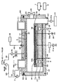
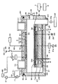
- the plasma etching processing apparatus includes a processing container 21 composed of a vacuum chamber, and a mounting table 3 disposed at the center of the bottom surface in the processing container 21.
- the processing container 21 is electrically grounded, and an exhaust port 22 is formed at a side position of the mounting table 3 on the bottom surface of the processing container 21.
- the exhaust port 22 is connected to a vacuum exhaust means 23 including a vacuum pump or the like via an exhaust pipe 24 provided with a pressure adjustment valve 24a which is a pressure adjustment means.
- a transfer port 25 for carrying in and out the wafer W is provided on the side wall of the processing vessel 21, and the transfer port 25 is configured to be opened and closed by a gate valve 26.
- the mounting table 3 includes a lower electrode 31 and a support 32 that supports the lower electrode 31 from below, and is disposed on the bottom surface of the processing vessel 21 via an insulating member 33.
- An electrostatic chuck 34 is provided on the top of the mounting table 3, and a voltage is applied to the electrostatic chuck 34 from a high-voltage DC power source 35 via a switch 35 a, so that the wafer W is statically placed on the mounting table 3. Electroadsorbed. Inside the mounting table 3, a temperature control channel 37 through which the temperature control medium flows is formed, and the temperature of the wafer W is adjusted by this temperature control medium.
- a gas flow path 38 for supplying a thermally conductive gas as a backside gas to the back surface of the wafer W is formed inside the mounting table 3, and this gas flow path 38 is formed on the upper surface of the mounting table 3. It communicates with openings provided at a plurality of locations.
- the aforementioned electrostatic chuck 34 has a plurality of through holes 34a communicating with the gas flow path 38, and the backside gas is supplied to the back side of the wafer W through the through holes 34a. Is done.
- a bias high frequency power supply 31a having a frequency of 13.56 MHz and a power of 0 to 4000 W is connected to the lower electrode 31 via a matching unit 31b.
- the high-frequency bias supplied from the high-frequency power supply 31a is for attracting ions in the plasma toward the wafer W, as will be described later.
- the high frequency supplied to the lower electrode 31 can be the same as the high frequency supplied to the gas shower head 4 described later.
- a so-called single-frequency excitation type plasma etching apparatus that applies high-frequency power only to the upper electrode without providing the high-frequency power supply 31a may be used.
- a focus ring 39 is disposed on the outer peripheral edge of the lower electrode 31 so as to surround the electrostatic chuck 34, and the plasma is configured to converge on the wafer W on the mounting table 3 through the focus ring 39. Has been.
- a gas shower head 4 is disposed on the top wall of the processing vessel 21 as an upper electrode and a processing gas supply unit so as to face the mounting table 3.
- the gas shower head 4 is made of an electrode portion 42 made of a conductive member such as aluminum having a circular depression on the lower surface, and a conductive member provided so as to cover the lower surface of the electrode portion 42 such as polycrystalline silicon.
- a support member 43 forming a disc-shaped shower plate.
- the conductive member may be a semiconductor as in this example, but may be a conductor (good conductor) such as a metal.
- a space defined by the electrode portion 42 and the support member 43 forms a gas diffusion space 41 in which the processing gas diffuses.
- the region between the wafer W on the mounting table 3 and the gas shower head 4 forms a processing region.
- the gas shower head 4 is connected to a first high-frequency power supply unit 4a having an output frequency of 40 MHz and power of 500 to 3000 W, for example, for forming an electric field for generating plasma in the processing region via a matching unit 4b. Yes.
- a processing gas supply path 45 communicating with the gas diffusion space 41 is formed at the center of the electrode part 42.
- a processing gas supply system 49 is connected to the upstream side of the processing gas supply path 45 via a gas supply pipe 48.
- the processing gas supply system 49 is for supplying a processing gas to the wafer W.
- an etching gas for performing an etching process such as a fluorocarbon gas, a chlorine (Cl 2 ) gas, one Carbon oxide (CO) gas, hydrogen bromide (HBr) gas, O 3 (ozone) gas, or the like can be supplied into the processing vessel 21 together with a diluent gas such as Ar (argon) gas.
- the processing gas supply system 49 is connected to each of a plurality of branch passages provided with valves and flow rate adjusters, and the above-described etching gas and the like. And a gas source in which a dilution gas is stored, and is configured so that a predetermined etching gas or Ar gas can be supplied at a desired flow rate ratio in accordance with the type of film to be etched.
- the support member 43 is airtightly pressure-bonded to the electrode portion 42 via, for example, a seal member (not shown) provided on the periphery of the upper surface thereof.
- a seal member (not shown) provided on the periphery of the upper surface thereof.
- gas discharge holes 44 are arranged in the support member 43 so that gas can be supplied from the gas diffusion space 41 to the wafer W with high in-plane uniformity.
- a temperature control fluid passage (not shown) is formed in the gas shower head 4, and the temperature of the gas shower head 4 can be adjusted by the temperature control fluid flowing through the temperature control fluid passage. ing.
- the ring-shaped region surrounding the gas shower head 4 described above in the top wall portion of the processing vessel 21 forms the outer top plate 60 and is made of a dielectric material such as quartz.
- the outer top plate 60 and the gas shower head 4 are airtightly pressure-bonded via a seal member (not shown) formed in a ring shape on the inner peripheral end of the outer top plate 60, for example.
- the outer top plate 60 and the gas shower head 4 are fixed so as to have the same height as the lower surfaces of both.
- the outer top plate 60 is supported by the side wall of the processing container 21 at the outer peripheral end thereof.
- the lower surface of the outer peripheral end of the outer top plate 60 is at a higher position than the lower surface of the inner peripheral portion of the outer top plate 60, so that the top wall (the gas shower head 4 and the outer top plate 60) of the processing container 21 is in the processing container.
- the gas shower head 4 and the mounting table 3 come close to each other.
- a ring-shaped groove 61 is formed in the upper end surface of the side wall of the processing container 21 in the circumferential direction, and a sealing member 62 such as an O-ring is accommodated in the groove 61.
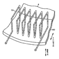
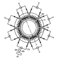
- the induction coil 70 which is an induction conductor in which a plurality of conductive wires made of metal, for example, are wound around the outer top plate 60, is equally spaced at a plurality of locations, for example, eight locations in the circumferential direction. Is provided.
- the axis of each induction coil 70 substantially coincides with an arc along the outer edge of the wafer W.
- Each induction coil 70 has a rectangular cross section, and the upper and lower surfaces thereof are parallel to the surface of the wafer W on the mounting table 3. As shown in FIG. 1, the induction coil 70 is actually provided so that the lower side enters the inside of the outer top plate 60. In FIG. 2 and FIG. It is drawn.
- induction coils 70 are electromagnetically induced through the outer top plate 60 in the region below the induction coil 70 in the processing container 21, that is, in the peripheral region surrounding the lower space (processing region) of the gas shower head 4.
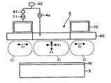
- a second electric field E2 extending radially (amplifies) in the lateral direction is formed along the line connecting the sidewall of the processing chamber 21 and the upper region of the central portion of the wafer W over the circumferential direction.
- the plurality of induction coils 70 have, for example, a common output frequency of 40 MHz which is the same as the output frequency of the first high frequency power supply unit 4a described above and a power of 200 to 1200 W.
- Each of the second high frequency power supply units 71 is connected in parallel via a conductive path 72.
- these induction coils In addition, in order to align the phase of the second electric field E2 that repeats the amplitude between the direction from the center side toward the outer periphery side and the direction from the outer periphery side toward the center portion side in the circumferential direction, these induction coils
- the plurality of conductive paths 72 that connect between 70 and the second high-frequency power supply unit 71 have the same length. Further, in order to make the magnitudes of the electric fields E2 formed by the induction coils 70 uniform, the plurality of conductive paths 72 have, for example, the same diameter so that the impedances are uniform. In FIG. 3, only one induction coil 70 is shown enlarged for convenience. In addition, although the illustration is simplified in FIGS. 2 and 3, the induction coil 70 is wound many times.
- FIG. 1 described above shows a longitudinal sectional view when the processing vessel 21 is cut along the line AA in FIG.
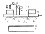
- the high frequency power from the first high frequency power supply unit 4a is supplied to the upper electrode (gas shower head 4), an electric field is formed between the gas shower head 4 and the lower electrode (mounting table 3).
- a first electric field E1 is formed between the region near the lower surface of the gas shower head 4 in the processing container 21 and the side wall of the processing container 21 in the horizontal direction (oscillating in the horizontal direction). More specifically, the direction of the first electric field E1 is along a line extending radially from the central portion of the processing vessel 21 when viewed from above.
- the second electric field E2 formed in the processing container 21 by supplying high-frequency power to the induction coil 70 by the second high-frequency power supply unit 71 In order to adjust the strength of the combined electric field of the first electric field E1, the phases of the electric fields E1 and E2 are adjusted.
- the output frequencies of the first high frequency power supply unit 4a and the second high frequency power supply unit 71 are set to the same value, and the high frequency output from the first high frequency power supply unit 4a and the second high frequency power supply unit 71
- the system is configured so that the phase difference from the output high frequency can be adjusted. An example of a method for adjusting such a phase difference is given below.
- Each of the first high-frequency power supply unit 4a and the second high-frequency power supply unit 71 is configured to generate a high frequency based on a clock input from the outside.
- a clock generation source 92 is provided outside, and a signal line (signal path 95) is distributed from the clock generation source 92 to the first high-frequency power supply unit 4a and the second high-frequency power supply unit 71, and any one of the distribution signal lines is distributed.
- the phase shifter 91 is interposed at 95. The phase shifter 91 adjusts the phase of the clock signal based on an analog signal or a digital signal from the controller, whereby the phase difference between the first electric field E1 and the second electric field E2 is a desired value, for example, the same phase.
- phase difference of each high frequency of the 1st high frequency power supply part 4a and the 2nd high frequency power supply part 71 is adjusted so that it may become a reverse phase.
- setting the electric fields E1 and E2 to the same phase or opposite phases means that the phase difference between the high frequencies output from the first and second high frequency power supply units 4a and 71 is, for example, the same phase or the opposite phase. This can be achieved.
- the plasma density is higher on the peripheral side than on the central side of the processing region.
- the reverse phase it is understood that the plasma density is higher on the central side than on the peripheral side of the processing region.
- a controller 7 is connected to the plasma etching apparatus.
- the control unit 7 includes a CPU 11, a program 12, a work memory 13 for work, and a memory 14 as a storage unit.
- the memory 14 includes a type of a film to be etched (film to be etched), a type of etching gas, a gas flow rate, a processing pressure, a magnitude of electric power of the first high frequency power supply unit 4 a supplied to the gas shower head 4, and An area in which processing conditions such as the magnitude of the electric power of the second high frequency power supply 71 supplied to the induction coil 70 and the high frequency phase adjusted by the phase shifter 91 are written is provided for each recipe.
- the type of etching gas differs for each film, Also, the processing conditions such as the flow rate of etching gas and processing pressure are different for each film. For this reason, depending on the processing conditions, the plasma concentration distribution may vary in the radial direction of the wafer W, as shown in the examples described later.
- the plasma concentration is made uniform in the radial direction.
- the plasma concentration is high on the central side
- the plasma is extended to the peripheral side
- the plasma concentration is high on the peripheral side
- the plasma is pushed into the central side.
- the phase of the first electric field E1 formed (amplified) in the processing region is shown in FIG.
- FIG. 5B when the plasma concentration on the peripheral edge side of the wafer W increases, the second electric field E2 in the peripheral area is in phase with the same phase.
- the phase of the high frequency (voltage) supplied to the second high frequency power supply unit 71 by the phase shifter 91 is set for each film (processing condition) so that the second electric field E2 has an opposite phase to the electric field E1. It is adjusting. Since the electric fields E1 and E2 are oscillating in the horizontal direction in FIG. 5, the directions (phases) of the electric fields E1 and E2 at a certain moment are schematically shown in FIG. Moreover, the arrow shown in the induction coil 70 has shown the direction of the high frequency which is flowing through the said induction coil 70, when this electric field E2 is formed.
- the memory 14 stores an appropriate value of the factor obtained by, for example, performing experiments and calculations in advance for each recipe (for example, for each etching target film and for each processing condition).
- the program 12 reads the above-described recipe from the memory 14 to the work memory 13 for work for each film to be etched, and sends control signals to each part of the plasma etching apparatus according to the recipe. Instructions are incorporated so that the etching process is performed by advancing each step described below.
- This program (including programs related to processing parameter input operations and display) 12 is stored in a storage medium 8 such as a hard disk, a compact disk, a magnetic optical disk, or a memory card, and is installed in the control unit 7 from this storage medium 8.
- a storage medium 8 such as a hard disk, a compact disk, a magnetic optical disk, or a memory card
- a semiconductor wafer (hereinafter referred to as “wafer”) W which is a substrate to be processed, will be briefly described.
- This wafer W is, for example, a photoresist mask patterned with a predetermined pattern, for example, an antireflection film made of an organic substance, an amorphous A laminated film composed of a carbon film, an insulating film (SiO 2 film or SiCOH film) or a Poly-Si (polycrystalline silicon) film and an etching stop film made of, for example, an inorganic film is laminated on the silicon film in this order from the top. It is configured.
- a recipe corresponding to the film to be etched formed on the surface of the wafer W is read from the memory 14 to the work memory 13.
- the film to be etched on the surface layer is, for example, an antireflection film
- a recipe corresponding to this film is read out.
- the wafer W is loaded into the processing container 21 from the vacuum transfer chamber maintained in a vacuum atmosphere by the substrate transfer means (none of which is shown), placed on the mounting table 3 and sucked and held, and then the gate valve 26. Close.
- the inside of the processing vessel 21 is fully opened by, for example, the pressure adjusting valve 24a by the vacuum exhaust means 23, and the temperature is adjusted to a predetermined temperature from the temperature adjusting channel 37 and the gas channel 38.
- the medium and the backside gas are supplied to adjust the wafer W to a predetermined temperature.
- the control unit 7 outputs a control signal to a controller (not shown), whereby the controller adjusts the phase shifter 91 so that the phase shift amount stored in the recipe is obtained.
- high frequency power of 40 MHz is output from the first high frequency power supply unit 4a and the second high frequency power supply unit 71 with a phase difference corresponding to the adjusted phase shift amount.
- a high-frequency electric field is formed between the gas shower head 4 and the mounting table 3, but the first electric field E1 in the lateral (radial) direction is also generated as described above.
- a second electric field E ⁇ b> 2 that vibrates along a line extending in the lateral (radial) direction and roughly speaking radially is formed in the peripheral region of the processing vessel 21. It is formed.
- a high frequency for bias having a frequency of, for example, 13.56 MHz and a power of, for example, 500 W is supplied to the mounting table 3 from the high frequency power supply 31a.
- the processing gas is a combined electric field of the first electric field E1 and the second electric field E2, in other words, the first electric field E1 whose magnitude is adjusted by the second electric field E2 contributes to the generation of plasma. To do.
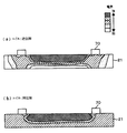
- the plasma concentration in the processing region is closer to the center side than the peripheral side as shown in FIG.
- the phase shifter 91 is adjusted so that the electric field E1 and the electric field E2 have the same phase as shown in FIG. For this reason, a combined electric field spread toward the peripheral edge side is formed, that is, the apparent electric field E1 is apparently spread toward the peripheral edge side, and the plasma concentration is made uniform over the processing region.
- an electric field E2 is formed in the peripheral region, and the strength of each of the electric fields E1 and E2 is adjusted by appropriately adjusting the respective high-frequency power supplied from the high-frequency power sources 4a and 71 as described above. Therefore, the electric field E1 pushed outward is overlapped with the electric field E2, and uniform plasma is formed over the surface as shown in FIG.
- the phase shifter 91 is adjusted so that the electric fields E1 and E2 have opposite phases.
- the plasma concentration is made uniform over the processing region, and the intensity of the electric fields E1 and E2 is adjusted appropriately, so that plasma with a uniform concentration is formed over the surface. It will be.
- FIGS. 7 and 9 the portion where the plasma concentration is high is hatched. When the plasma comes into contact with the processing gas, the processing gas is also converted into plasma, and plasma is sequentially generated.
- the etching process with high perpendicularity proceeds. Then, the antireflection film is etched until the amorphous carbon film under the antireflection film is exposed.
- the supply of the processing gas is stopped, and the high-frequency supply to the induction coil 70 and the gas shower head 4 is stopped.
- the inside of the processing container 21 is evacuated, and then a recipe corresponding to the amorphous carbon film to be etched is read from the memory 14 and the amorphous carbon film is etched. Thereafter, the recipe is sequentially read out and etched in the same manner for the lower layer of the amorphous carbon film.
- the induction coil 70 is disposed so as to surround the gas shower head 4 connected to the first high-frequency power supply unit 4 a when viewed from above, and is induced by the second high-frequency power supply unit 71.
- a high frequency power is supplied to the coil 70 to form a horizontal electric field E2 in the processing container 21 along a line connecting the side wall of the processing container 21 and the upper region of the central portion of the wafer W.
- a combined electric field is formed by a horizontal (diameter) electric field E1 formed in the vicinity of the gas shower head 4 by one high-frequency power supply unit 4a.
- the electric field E1 can be pushed into the central portion side or extended toward the peripheral portion side, so that the plasma concentration distribution in the radial direction can be made uniform according to the processing recipe. Therefore, since the plasma concentration can be made uniform over the surface, plasma processing with high in-plane uniformity can be performed on the wafer W, in this example, etching processing. Further, since the plasma concentration in the processing region can be adjusted simply by adjusting the phase of the high frequency supplied to the second high frequency power supply unit 71, the plasma concentration can be easily adjusted according to the film (recipe) to be etched. .
- the amount of plasma that is extended to the peripheral side or pushed into the central side can be adjusted, Since the plasma concentration in the processing region and the peripheral region can be made uniform, the plasma concentration can be made uniform over the entire surface.
- each induction coil 70 is formed in an arc shape, and is formed in a square shape so that the upper and lower surfaces of each induction coil 70 are horizontal.
- the electric field E2 in the lateral (diameter) direction is formed. For example, it may be formed in a circular shape.
- the gas shower head 4 is connected to the first high-frequency power supply unit 4a to form a single-frequency excitation type plasma etching processing apparatus using only the upper electrode, or the mounting table 3
- a high frequency power source 31a is connected to the upper electrode and the lower electrode to form a dual frequency excitation plasma etching apparatus.
- the first high frequency power supply unit 4a may be connected to the mounting table 3 so as to be a one-frequency excitation type or two-frequency excitation type device using only the lower electrode.
- the dielectric member 101 is disposed around the mounting table 3 in the circumferential direction, and the induction coil 70 is disposed below the dielectric member 101. become.
- the exhaust port 22 is formed on the top wall of the processing vessel 21, for example, the outer top plate 60 or the side wall of the processing vessel 21.
- the outer top plate 60 is made of a conductor, it is preferable to provide a ring-shaped insulating member 102 between the outer top plate 60 and the gas shower head 4.
- the plasma etching process is performed similarly to the above example, and the same effect can be obtained.
- the rectangular induction coil 70 has been described.
- the second embodiment in order to form the second electric field E2, for example, as shown in FIG.
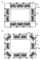
- a plurality of conductive wires 111 are arranged radially over the circumferential direction.
- a plurality of conductors are provided in a ring-shaped flat plate 112 made of, for example, a dielectric so that the inner and outer peripheral ends of the conductor 111 are exposed.
- 111 is embedded, and this flat plate 112 is installed on the outer top plate 60 together with the plurality of conductive wires 111.
- the conductive path 72 may be disposed.
- the second high frequency power supply unit 71 is provided above the gas shower head 4 and one conductive path 72 extending from the second high frequency power supply unit 71 as shown in FIG. Are branched into two, and each of the two conductive paths 72 is similarly branched into two, thus sequentially branching the conductive paths 72 to form a plurality of conductive paths 72 each having the same length. .
- the end portions of the plurality of conductive paths 72 are connected to one end side, for example, the outer peripheral end of each conductive wire 111, and similarly, as shown in FIG. 13B, the other end side of the conductive wire 111, for example, the inner peripheral end.
- the second high frequency power supply unit 71 is connected to a plurality of other conductive paths 72 each having the same length, and the second high frequency power supply unit 71 and each of the conductive wires 111 have the same length. Will be connected.
- the conductive wire 111 is schematically shown in a linear shape, and in FIG. 13, the number of the conductive wires 111 drawn is smaller than the actual number.
- the drawing of the flat plate 112 is omitted.
- the conductive path 72 is connected to both ends of all the conductive wires 111.
- the conductive path 72 is drawn separately in FIGS. 13 (a) and 13 (b). ing.
- the same effect is obtained by performing the plasma etching process in the same manner.
- the impedance of each conducting wire 111 is smaller than when the square induction coil 70 is provided, plasma can be generated efficiently.
- the conducting wire 111 may be installed in the lower part of the processing vessel 21 as in FIG.
- a ring body 200 made of a metal such as aluminum (Al) or copper (Cu) may be provided on the outer top plate 60 as shown in FIG. .
- reference numeral 211 denotes slits formed at a plurality of locations from the inner peripheral side of the ring body 200 toward the radial direction (outer side), and 212 supplies current between the inner peripheral side and the outer peripheral side of the ring body 200. A plurality of contact points. By supplying a high-frequency current between these contacts 212 and 212, a radial electric field E2 is formed in the radial direction in the same manner as the conductive wire 111 described above.
- a high frequency is supplied from the common second high frequency power supply unit 71 to the plurality of induction coils 70.
- the second high frequency power supply unit 71 is connected to each induction coil 70.
- each conductive path 72 is set to have the same length so that the impedance between each second high-frequency power source 71 and each induction coil 70 has the same value.
- a common phase shifter 91 is connected to the plurality of second high frequency power supply units 71, and the impedance between the phase shifter 91 and the plurality of second high frequency power supply units 71 is the same value.
- the signal path 95 is set to the same length.
- plasma etching may be performed in the same manner as in the above examples.
- the plasma concentration distribution in the circumferential direction of the wafer W May be configured to be uniform.
- the high-frequency power or transfer supplied from the above-described processing conditions and the high-frequency power supply unit 4a for each recipe, the high-frequency power or transfer supplied from the above-described processing conditions and the high-frequency power supply unit 4a.
- the magnitude of each high-frequency power supplied to each induction coil 70 is stored so that the plasma concentration in the circumferential direction of the wafer W is made uniform. An area is provided.
- the high-frequency power supplied to each induction coil 70 is obtained by conducting experiments and calculations in advance.
- the plasma concentration is made uniform in the circumferential direction in addition to the plasma concentration in the radial direction, and the etching process is highly perpendicular throughout the surface. Will be done.
- a common phase shifter 91 is connected to each second high frequency power supply unit 71, but a separate phase shifter 91 is connected to each second high frequency power supply unit 71. It may be provided.
- the induction coil 70 may be installed on the lower side of the processing vessel 21 as shown in FIG. 11, and a plurality of conductors 111 are used as the induction coil 70 as shown in FIGS. And a plurality of second high frequency power supply units 71 may be connected to the plurality of conducting wires 111, respectively.
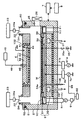
- a DC power supply 53 for applying a negative DC voltage of 0 to ⁇ 2000 V, for example, is connected to the electrode section 42 described above as a negative voltage supply means via a switch 52.
- the DC power source 53 is for forming a sheath 121 having a thickness corresponding to the magnitude of voltage in a region below the gas shower head 4 when plasma is generated.
- the sheath 121 can draw the electric field E2 formed (induced) by the induction coil 70 at the peripheral edge of the processing region toward the center of the processing region. Accordingly, in the memory 14 described above, as shown in FIG.
- the processing conditions the magnitude of the high frequency voltage supplied from the high frequency power sources 4a and 71, the phase of the high frequency adjusted by the phase shifter 91, etc.
- the magnitude of the negative DC voltage applied to the DC power supply 53 is stored.
- the magnitude of the negative DC voltage is also obtained by conducting experiments and calculations in advance.
- the sheath 121 is used to center the processing vessel 21. Since the electric field E2 drawn to the part side is also adjusted, the density of the electric field is further uniformed in the plane, so that the amount of plasma is also uniformed in the plane and the etching process is uniform. Can be done.
- the induction coil 70 may be provided in the lower part of the processing vessel 21 as shown in FIG. 11, or the conductive wire 111 is arranged instead of the induction coil 70 as shown in FIGS.
- the second high frequency power supply unit 71 may be individually connected to the plurality of induction coils 70 or the plurality of conductive wires 111.
- FIG. 20A a processing vessel 21 and a gas shower head 4 having a square shape when viewed from above are used. Further, the induction coil 70 is wound around an axis extending linearly along the outer edge of the LCD substrate G as viewed from above.
- a horizontal electric field is formed along a line connecting the side wall of the processing vessel 21 and the upper region in the center of the LCD substrate G.
- the above-mentioned line refers to a line that extends from the side wall of the processing container 21 in a horizontal and orthogonal manner to either the vertical or horizontal side of the LCD substrate G. Even in such a rectangular LCD substrate G, the etching process is uniformly performed similarly to the wafer W described above, and the same effect can be obtained.
- the processing of corner portions may vary.
- an induction coil 70a may be arranged so as to face the corner portion.
- the induction coil 70 may be disposed below the processing container 21 as described above, or instead of the induction coil 70.
- the conducting wire 111 may be provided, a plurality of second high frequency power supply units 71 may be individually connected to the plurality of induction coils 70 and the conducting wire 111, or the negative DC power supply 53 may be provided.
- the induction coil 70 is also supplied with high frequency. Since the energy supplied into the processing vessel 21 is increased as compared with the case where no 70 is provided, plasma can be easily obtained.
- the phase shifter 91 is interposed between the clock generation source 92 and the second high frequency power supply unit 71 in adjusting the high frequency phase.
- the phase shifter 91 is interposed between the clock generation source 92 and the first high frequency power supply unit 4a without being provided between the clock generation source 92 and the second high frequency power supply unit 71, so that the first You may make it adjust the phase of the high frequency supplied to the high frequency power supply part 4a.
- the high frequency power supplied to the gas shower head 4 may be shared by a plurality of recipes, and the plasma concentration in the radial direction may be adjusted by the high frequency power supplied to the induction coil 70.
- phase shifter 91 is provided between the clock generation source 92 and the first high frequency power supply unit 4a and the second high frequency power supply unit 71, and each of the high frequency phases supplied to the respective high frequency power supplies 4a and 71 is provided. May be adjusted. Furthermore, although a high frequency is supplied from the common clock generation source 92 to the first high frequency power supply unit 4a and the second high frequency power supply unit 71, different clock generation sources 92 and 92 may be connected to each other. .
- a phase shifter 91 may be provided between each of the clock generation source 92 and the first high-frequency power supply unit 4a and the second high-frequency power supply unit 71, or one high-frequency power supply 4a (71 ) And the other high-frequency power supply 71 (4a) are obtained in advance, and a phase shifter 91 is provided only in one high-frequency power supply 4a (71), and the other high-frequency power supply 71 (4a) is provided.
- the phase of one high-frequency power supply 4a (71) with respect to () may be adjusted.
- the frequency of the high frequency supplied to the gas shower head 4 and the induction coil 70 is not limited to the above 40 MHz, and may be another frequency, for example, 13.56 MHz or 100 MHz used in the embodiments described later. Alternatively, other frequencies such as 60 MHz may be used.
- the high frequency supplied from the first high frequency power supply unit 4a and the second high frequency power supply unit 71 has the same phase (phase difference: 0 degree) or opposite phase (phase difference: 180 degree). However, you may adjust the phase shifter 91 so that it may become another phase difference, for example, 45 degree
- the induction coil 70 (the conductive wire 111) is installed outside the internal space of the processing vessel 21, but the outer top plate 60 (the dielectric member 101) is divided into an upper portion and a lower portion.
- the body may be configured as a body (none of which is shown), and a plurality of concave portions may be formed in the lower portion at regular intervals, for example, in the circumferential direction, and the induction coil 70 (conductor 111) may be accommodated in the concave portions. . Further, for example, the induction coil 70 (conductor 111) may be installed in the internal space of the processing container 21.
- the plasma processing apparatus of the present invention may be applied to, for example, a film formation processing apparatus using a CVD (Chemical Vapor Deposition) method using plasma, or may be applied to an ashing apparatus.
- CVD Chemical Vapor Deposition
- the magnitude of the high frequency power supplied from the high frequency power supplies 4a and 71 and the phase of the high frequency adjusted by the phase shifter 91 according to the processing conditions such as the type of film forming gas, the gas flow rate, and the pressure are adjusted.
- the film is stored in the recipe, and the film forming process is performed at a uniform film forming speed within the surface.
- Example 1 When high-frequency power is supplied from the high-frequency power source 4a to the gas shower head 4 to turn the processing gas into plasma without supplying high frequency to the induction coil 70, how the plasma (electrons) in the surface is distributed according to the processing conditions. An experiment was conducted to confirm whether to do this. The experiment was performed at a low pressure (2.7 Pa (20 mTorr)) and a high pressure (13.3 Pa (100 mTorr)), and the plasma density from the center to the periphery of the inner space of the processing vessel 21 was measured using a Langmuir probe. It was measured.
- FIG. 21A shows a result obtained when the pressure in the processing container 21 is low, for example.
- Example 2 Therefore, an experiment was conducted to check how the plasma density changes by supplying high frequency from the high frequency power source 4a to the gas shower head 4 and supplying high frequency to the induction coil 70.
- the processing conditions first high frequency power supply unit 4a: 13.45 MHz, 50 V
- the processing conditions were adjusted so that the plasma concentration in the processing vessel 21 was uniform without using the induction coil 70.
- a high frequency having the same frequency as the first high frequency power supply unit 4a (13.56 MHz) and a voltage of 20V is supplied from the second high frequency power supply unit 71 to the induction coil 70, and the distribution of this plasma is determined. How it changes.
- FIG. 22A shows the plasma density to be compared.
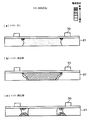
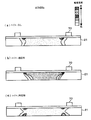
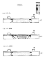
- FIG. 22B and FIG. 23A show the electric field E2 in reverse phase with respect to the electric field E1, and FIG. 22C and FIG. ) Shows the plasma density distribution when the phase of the high frequency is adjusted so that the electric field E1 and the electric field E2 have the same phase.
- the plasma is pushed into the central portion, that is, the electric field E1 is confined to the central portion.
- the plasma is attracted to the peripheral edge side, but the plasma absorbed by the side wall of the processing vessel 21 is hardly seen, so that the energy loss of the plasma is almost not. I knew it was not happening. Therefore, by adjusting the phase of the high frequency supplied to the induction coil 70 so that the electric field E1 and the electric field E2 have the same phase or opposite phases, the plasma density can be adjusted so that the plasma concentration becomes uniform in the plane. I understood.
- Example 4 A result obtained by changing the frequency of the high frequency supplied to the gas shower head 4 and the induction coil 70 to 40 MHz (FIG. 25) and 100 MHz (FIG. 26) using the same numerical simulation as in Experimental Example 3 above will be shown. As a result, it has been found that the same result can be obtained without depending on the frequency of the high frequency supplied to the gas shower head 4 and the induction coil 70.
Landscapes
- Physics & Mathematics (AREA)
- Engineering & Computer Science (AREA)
- Plasma & Fusion (AREA)
- Chemical & Material Sciences (AREA)
- Analytical Chemistry (AREA)
- Plasma Technology (AREA)
- Drying Of Semiconductors (AREA)
Abstract
Description
本発明のプラズマ処理装置をプラズマエッチング装置に適用した第1の実施の形態について、図1~図4を参照して説明する。このプラズマエッチング処理装置は、真空チャンバからなる処理容器21と、この処理容器21内の底面中央に配設された載置台3と、を備えている。処理容器21は電気的に接地されており、またこの処理容器21の底面における載置台3の側方位置には排気口22が形成されている。この排気口22には、圧力調整手段である圧力調整バルブ24aを備えた排気管24を介して真空ポンプ等を含む真空排気手段23が接続されている。処理容器21の側壁には、ウェハWの搬入出を行うための搬送口25が設けられており、この搬送口25はゲートバルブ26により開閉可能に構成されている。
上記の第1の実施の形態においては、角形の誘導コイル70について説明したが、この第2の実施の形態では、第2の電界E2を形成するために、例えば図12に示すように、直線状の導線111を周方向に亘って放射状に複数本配置している。この第2の実施の形態においては、図12(b)に示すように、導線111の内周端と外周端とが露出するように例えば誘電体からなるリング状の平板112内に複数の導線111を埋設し、この平板112を複数の導線111と共に外側天板60上に設置することになる。
この第2の実施の形態においても、同様にプラズマエッチング処理が行われて同様の効果が得られる。また、角型の誘導コイル70を設ける場合よりも、各々の導線111のインピーダンスが小さくなるので、効率的にプラズマを生成させることができる。この場合においても、既述の図11と同様に処理容器21の下部に導線111を設置しても良い。
既述の第1の実施の形態においては、共通の第2の高周波電源部71から複数の誘導コイル70に高周波を供給したが、この第3の実施の形態では、例えば図15に示すように、各々の誘導コイル70毎に第2の高周波電源部71を接続している。この場合においても、各々の第2の高周波電源部71と各々の誘導コイル70との間におけるインピーダンスが同じ値となるように、各々の導電路72が同じ長さに設定される。また、これらの複数の第2の高周波電源部71には共通の移相器91が接続され、移相器91とこれらの複数の第2の高周波電源部71との間におけるインピーダンスが同じ値となるように、信号路95が同じ長さに設定される。
次に、本発明の第4の実施の形態について説明する。既述の電極部42には、図17に示すように、スイッチ52を介して例えば0~-2000Vの負の直流電圧を印加するための直流電源53が負電圧供給手段として接続されている。この直流電源53は、図18に示すように、プラズマの発生時にガスシャワーヘッド4の下方側の領域に電圧の大きさに応じた厚さのシース121を形成するためのものである。このシース121によって誘導コイル70により処理領域の周縁部に形成(誘導)される電界E2を当該処理領域の中央部側に引き寄せることができる。従って、既述のメモリ14には、図19に示すように、レシピ毎に、処理条件や高周波電源4a、71から供給する高周波電圧の大きさ及び移相器91により調整する高周波の位相などに加えて、直流電源53に印加する負の直流電圧の大きさが記憶されている。この負の直流電圧の大きさについても、予め実験や計算を行うことにより求められることになる。
上記の各実施形態においては円形のウェハWの処理のための構成について説明したが、この第5の実施の形態で説明するように、角型の基板例えばLCD(Liquid Crystal Display:液晶ディスプレイ)用のガラス基板(以下、LCD基板という)Gの処理のために本発明を適用しても良い。
この場合には、図20(a)に示すように、上方から見たときの平面形状が角型の処理容器21及びガスシャワーヘッド4が用いられる。また、誘導コイル70は、上方から見て、LCD基板Gの外縁に沿って直線状に伸びる軸の回りに巻回されることになる。この第5の実施形態においては、上から見たときに処理容器21の側壁とLCD基板Gの中央の上方領域とを結ぶラインに沿って横方向の電界が形成されることになる。なお、ここで、上記のラインとは、処理容器21の側壁からLCD基板Gの縦横のいずれかの辺に水平に直交して伸びるラインを言う。このような角型のLCD基板Gにおいても、既述のウェハWと同様にエッチング処理が均一に行われ、同様の効果が得られる。
誘導コイル70に高周波を供給せずに、高周波電源4aからガスシャワーヘッド4に高周波を供給して処理ガスをプラズマ化した時に、面内におけるプラズマ(電子)が処理条件に応じてどのように分布するか確認する実験を行った。実験は低圧力(2.7Pa(20mTorr))及び高圧力(13.3Pa(100mTorr))にて行い、ラングミュアープローブ(Langmuir probe)を用いて処理容器21内部空間の中央から周縁におけるプラズマ密度を測定した。そして、図21(a)に例えば処理容器21内の圧力が低い場合について、図21(b)に例えば処理容器21内の圧力が高い場合について得られた結果を示す。この結果から、圧力が低い場合には、ガスシャワーヘッド4と対極(載置台3)とが電気的に結合し、統計(Stochastic)加熱となり、そのため中央部でのプラズマ密度が強くなり、逆に周縁部ではプラズマ密度が弱くなることが分かった。一方、圧力が高い場合には、ガスシャワーヘッド4と処理容器21の側壁とが電気的に結合し、誘導(Ohmic)加熱となり、そのため中央部側よりも周縁部側においてプラズマの密度が強くなることが分かった。このような中央部側と周縁部側とにおけるプラズマ密度の偏析は、圧力だけでなく様々な処理条件の変化に起因して生じていた。従って、既述のように、面内に亘って均一にプラズマエッチング処理を行うためには、処理条件毎にプラズマ密度を均一化する必要のあることが分かった。
そこで、ガスシャワーヘッド4に高周波電源4aから高周波を供給すると共に、誘導コイル70に高周波を供給することにより、プラズマ密度がどのように変化するかを確認する実験を行った。先ず、誘導コイル70を用いずに処理容器21内のプラズマの濃度が均一化するように処理条件(第1の高周波電源部4a:13.45MHz、50V)を調整した。そして、この処理条件において第1の高周波電源部4a(13.56MHz)と同じ周波数で電圧が20Vの高周波を第2の高周波電源部71から誘導コイル70に供給して、このプラズマの分布がどのように変化するか測定した。この時、電界E1に対して電界E2の向きが逆位相及び同位相となるように誘導コイル70に供給する高周波の位相を夫々調整して、これらの例と誘導コイル70に高周波を供給しなかった場合(比較対象)と比較した。この結果を図22及び図23に示す。
次に、上記の実験2の各例について、数値シミュレーションを用いて処理容器21内の全電流密度を計算した。この結果を図24に示す。この結果からも、電界E1に対して電界E2が逆位相となることによりプラズマが中央部側に押し込まれ、逆に電界E1と電界E2とが同位相となることによりプラズマが周縁部側に引き寄せられていることが分かった。
上記の実験例3と同じ数値シミュレーションを用いてガスシャワーヘッド4及び誘導コイル70に供給する高周波の周波数を40MHz(図25)及び100MHz(図26)に変えて行った結果を示す。その結果、ガスシャワーヘッド4及び誘導コイル70に供給する高周波の周波数に寄らずに同様の結果が得られることが分かった。
Claims (7)
- 処理容器と、前記処理容器内に設けられた下部電極である載置台と上部電極でありかつ処理ガスの供給部をなすガスシャワーヘッドとを備え、前記下部電極と前記上部電極との間にプラズマ発生用の高周波電力を印加して処理ガスをプラズマ化し、そのプラズマにより前記載置台上の基板に対してプラズマ処理を行うプラズマ処理装置において、
前記上部電極及び下部電極の一方の電極に接続され、前記プラズマ発生用の高周波電力を出力するための第1の高周波電源部と、
前記第1の高周波電源部の出力周波数と同じ出力周波数の高周波電力を出力するように設定された第2の高周波電源部と、
前記第1の高周波電源部に接続される前記一方の電極を上から見たときに当該一方の電極を囲むように配置され、前記第2の高周波電源部から供給される高周波電力により前記処理容器内に当該処理容器の側壁と前記基板の中央部の上方領域との間を結ぶラインに沿って横方向の電界を形成するための誘導コイルと、
第1の高周波電源部からの高周波電力が供給されることにより前記処理容器内における前記一方の電極付近に発生する横方向の電界と前記誘導コイルにより形成される前記横方向の電界とを合成した電界の強度を調整するために、第1の高周波電源部及び第2の高周波電源部から出力される各々の高周波の互いの位相差を調整するための位相差調整手段と、
を備えたことを特徴とするプラズマ処理装置。 - 合成した電界の強度の調整作業は、前記第1の高周波電源部により形成される前記横方向の電界と第2の高周波電源部により形成される前記横方向の電界とを同位相または逆位相に設定する作業であることを特徴とする請求項1に記載のプラズマ処理装置。
- 前記誘導コイルは、処理容器の周方向に沿って複数配置され、当該複数の誘導コイルの各々と前記第2の高周波電源部とを接続する各導電路の長さが互いに同じであることを特徴とする請求項1または2に記載のプラズマ処理装置。
- 前記ガスシャワーヘッドに接続され、前記誘導コイルにより誘導された前記電界を前記処理容器の中央部側に引き込むための負電圧供給手段を備えたことを特徴とする請求項1ないし3のいずれか一つに記載のプラズマ処理装置。
- 前記位相差調整手段は、前記第1の高周波電源部により形成される前記横方向の電界と第2の高周波電源部により形成される前記横方向の電界との位相差を調整するための制御信号を出力する制御部を備えていることを特徴とする請求項1ないし4のいずれか一つに記載のプラズマ処理装置。
- 前記制御部は、前記第1の高周波電源部により形成される前記横方向の電界と第2の高周波電源部により形成される前記横方向の電界とを同位相に調整するための制御信号と逆位相に調整するための制御信号とを選択的に出力する機能を備えていることを特徴とする請求項5に記載のプラズマ処理装置。
- 基板に対して行われる処理のレシピと、前記位相差調整手段による位相の調整量と、を対応づけて記憶した記憶部を備え、前記制御部は、この記憶部から前記レシピに応じた前記調整量を読み出して制御信号を出力することを特徴とする請求項5または6に記載のプラズマ処理装置。
Priority Applications (3)
| Application Number | Priority Date | Filing Date | Title |
|---|---|---|---|
| KR1020117009509A KR101255900B1 (ko) | 2008-11-18 | 2009-11-17 | 플라즈마 처리 장치 |
| CN2009801421804A CN102197464A (zh) | 2008-11-18 | 2009-11-17 | 等离子体处理装置 |
| US13/129,541 US20110240222A1 (en) | 2008-11-18 | 2009-11-17 | Plasma processing apparatus |
Applications Claiming Priority (2)
| Application Number | Priority Date | Filing Date | Title |
|---|---|---|---|
| JP2008-294871 | 2008-11-18 | ||
| JP2008294871A JP5391659B2 (ja) | 2008-11-18 | 2008-11-18 | プラズマ処理装置 |
Publications (1)
| Publication Number | Publication Date |
|---|---|
| WO2010058771A1 true WO2010058771A1 (ja) | 2010-05-27 |
Family
ID=42198210
Family Applications (1)
| Application Number | Title | Priority Date | Filing Date |
|---|---|---|---|
| PCT/JP2009/069492 Ceased WO2010058771A1 (ja) | 2008-11-18 | 2009-11-17 | プラズマ処理装置 |
Country Status (5)
| Country | Link |
|---|---|
| US (1) | US20110240222A1 (ja) |
| JP (1) | JP5391659B2 (ja) |
| KR (1) | KR101255900B1 (ja) |
| CN (1) | CN102197464A (ja) |
| WO (1) | WO2010058771A1 (ja) |
Families Citing this family (14)
| Publication number | Priority date | Publication date | Assignee | Title |
|---|---|---|---|---|
| US8869741B2 (en) * | 2008-12-19 | 2014-10-28 | Lam Research Corporation | Methods and apparatus for dual confinement and ultra-high pressure in an adjustable gap plasma chamber |
| US9396908B2 (en) * | 2011-11-22 | 2016-07-19 | Lam Research Corporation | Systems and methods for controlling a plasma edge region |
| JP6010305B2 (ja) * | 2012-02-07 | 2016-10-19 | 東京エレクトロン株式会社 | 誘導結合プラズマ用アンテナユニット、誘導結合プラズマ処理装置および誘導結合プラズマ処理方法 |
| US9161428B2 (en) | 2012-04-26 | 2015-10-13 | Applied Materials, Inc. | Independent control of RF phases of separate coils of an inductively coupled plasma reactor |
| US20130284369A1 (en) * | 2012-04-26 | 2013-10-31 | Applied Materials, Inc. | Two-phase operation of plasma chamber by phase locked loop |
| US9312106B2 (en) * | 2013-03-13 | 2016-04-12 | Applied Materials, Inc. | Digital phase controller for two-phase operation of a plasma reactor |
| JP6446418B2 (ja) * | 2016-09-13 | 2018-12-26 | 株式会社Kokusai Electric | 半導体装置の製造方法、基板処理装置およびプログラム |
| US11158489B2 (en) * | 2016-11-08 | 2021-10-26 | Applied Materials, Inc. | Methods and systems to modulate film stress |
| US11217434B2 (en) * | 2016-12-27 | 2022-01-04 | Evatec Ag | RF capacitive coupled dual frequency etch reactor |
| US10629415B2 (en) * | 2017-03-28 | 2020-04-21 | Asm Ip Holding B.V. | Substrate processing apparatus and method for processing substrate |
| US11551909B2 (en) * | 2017-10-02 | 2023-01-10 | Tokyo Electron Limited | Ultra-localized and plasma uniformity control in a plasma processing system |
| CN108695150B (zh) * | 2018-05-22 | 2020-11-27 | 朝阳微电子科技股份有限公司 | 一种半导体晶圆批量刻蚀方法 |
| CN108899275B (zh) * | 2018-07-20 | 2021-03-02 | 北京北方华创微电子装备有限公司 | 一种等离子体刻蚀方法 |
| US11655540B2 (en) * | 2020-06-26 | 2023-05-23 | Applied Materials, Inc. | Methods and apparatus for adjusting wafer performance using multiple RF generators |
Citations (1)
| Publication number | Priority date | Publication date | Assignee | Title |
|---|---|---|---|---|
| JP2003525519A (ja) * | 2000-03-01 | 2003-08-26 | 東京エレクトロン株式会社 | 高密度プラズマ源内での電気的に制御可能なプラズマ均一性 |
Family Cites Families (18)
| Publication number | Priority date | Publication date | Assignee | Title |
|---|---|---|---|---|
| TW249313B (ja) * | 1993-03-06 | 1995-06-11 | Tokyo Electron Co | |
| US5619103A (en) * | 1993-11-02 | 1997-04-08 | Wisconsin Alumni Research Foundation | Inductively coupled plasma generating devices |
| US5710486A (en) * | 1995-05-08 | 1998-01-20 | Applied Materials, Inc. | Inductively and multi-capacitively coupled plasma reactor |
| TW279240B (en) * | 1995-08-30 | 1996-06-21 | Applied Materials Inc | Parallel-plate icp source/rf bias electrode head |
| US5573595A (en) * | 1995-09-29 | 1996-11-12 | Lam Research Corporation | Methods and apparatus for generating plasma |
| US6178920B1 (en) * | 1997-06-05 | 2001-01-30 | Applied Materials, Inc. | Plasma reactor with internal inductive antenna capable of generating helicon wave |
| US6310577B1 (en) * | 1999-08-24 | 2001-10-30 | Bethel Material Research | Plasma processing system with a new inductive antenna and hybrid coupling of electronagnetic power |
| WO2003029513A1 (en) * | 2001-09-28 | 2003-04-10 | Tokyo Electron Limited | Hybrid plasma processing apparatus |
| JP3643580B2 (ja) * | 2002-11-20 | 2005-04-27 | 株式会社東芝 | プラズマ処理装置及び半導体製造装置 |
| JP3896128B2 (ja) * | 2004-07-29 | 2007-03-22 | シャープ株式会社 | 高周波プラズマ処理装置および高周波プラズマ処理方法 |
| US8012306B2 (en) * | 2006-02-15 | 2011-09-06 | Lam Research Corporation | Plasma processing reactor with multiple capacitive and inductive power sources |
| US8911590B2 (en) * | 2006-02-27 | 2014-12-16 | Lam Research Corporation | Integrated capacitive and inductive power sources for a plasma etching chamber |
| US20080124254A1 (en) * | 2006-05-22 | 2008-05-29 | Dae-Kyu Choi | Inductively Coupled Plasma Reactor |
| US7837826B2 (en) * | 2006-07-18 | 2010-11-23 | Lam Research Corporation | Hybrid RF capacitively and inductively coupled plasma source using multifrequency RF powers and methods of use thereof |
| KR100845285B1 (ko) * | 2006-09-08 | 2008-07-09 | 삼성전자주식회사 | 플라즈마 생성장치 및 생성방법 |
| JP2008198659A (ja) * | 2007-02-08 | 2008-08-28 | Tokyo Electron Ltd | プラズマエッチング方法 |
| US20080236490A1 (en) * | 2007-03-29 | 2008-10-02 | Alexander Paterson | Plasma reactor with an overhead inductive antenna and an overhead gas distribution showerhead |
| CN102089867B (zh) * | 2008-07-11 | 2013-11-27 | 东京毅力科创株式会社 | 等离子体处理装置 |
-
2008
- 2008-11-18 JP JP2008294871A patent/JP5391659B2/ja not_active Expired - Fee Related
-
2009
- 2009-11-17 KR KR1020117009509A patent/KR101255900B1/ko not_active Expired - Fee Related
- 2009-11-17 CN CN2009801421804A patent/CN102197464A/zh active Pending
- 2009-11-17 US US13/129,541 patent/US20110240222A1/en not_active Abandoned
- 2009-11-17 WO PCT/JP2009/069492 patent/WO2010058771A1/ja not_active Ceased
Patent Citations (1)
| Publication number | Priority date | Publication date | Assignee | Title |
|---|---|---|---|---|
| JP2003525519A (ja) * | 2000-03-01 | 2003-08-26 | 東京エレクトロン株式会社 | 高密度プラズマ源内での電気的に制御可能なプラズマ均一性 |
Also Published As
| Publication number | Publication date |
|---|---|
| KR20110059797A (ko) | 2011-06-03 |
| KR101255900B1 (ko) | 2013-04-17 |
| JP5391659B2 (ja) | 2014-01-15 |
| JP2010123689A (ja) | 2010-06-03 |
| CN102197464A (zh) | 2011-09-21 |
| US20110240222A1 (en) | 2011-10-06 |
Similar Documents
| Publication | Publication Date | Title |
|---|---|---|
| JP5391659B2 (ja) | プラズマ処理装置 | |
| CN102089867B (zh) | 等离子体处理装置 | |
| US11289308B2 (en) | Apparatus and method for processing substrate and method of manufacturing semiconductor device using the method | |
| US11276562B2 (en) | Plasma processing using multiple radio frequency power feeds for improved uniformity | |
| TWI611735B (zh) | 電漿處理裝置(一) | |
| JP5309847B2 (ja) | プラズマ処理装置 | |
| JP5514310B2 (ja) | プラズマ処理方法 | |
| JP6807775B2 (ja) | 成膜方法及びプラズマ処理装置 | |
| TWI423308B (zh) | A plasma processing apparatus, a plasma processing method, and a dielectric window for use therefor and a method of manufacturing the same | |
| JP2008172168A (ja) | プラズマ処理装置、プラズマ処理方法及び記憶媒体 | |
| US20160118284A1 (en) | Plasma processing apparatus | |
| JP7509997B2 (ja) | プラズマ処理装置 | |
| JP5479013B2 (ja) | プラズマ処理装置及びこれに用いる遅波板 | |
| JP2023550342A (ja) | 静磁場を使用するプラズマ一様性制御 | |
| JP5332362B2 (ja) | プラズマ処理装置、プラズマ処理方法及び記憶媒体 | |
| JP2016143616A (ja) | プラズマ処理装置 | |
| CN110770880A (zh) | 等离子处理装置 | |
| TWI791106B (zh) | 處理系統及處理方法 | |
| JP2000031121A (ja) | プラズマ放出装置及びプラズマ処理装置 | |
| KR102074323B1 (ko) | 플라즈마 발생 장치 | |
| TW201842532A (zh) | 有機材料的自我限制蝕刻之實行程序 | |
| JP7223507B2 (ja) | エッチング方法 | |
| KR101994480B1 (ko) | 게이트 절연막 형성 방법 | |
| JP5728565B2 (ja) | プラズマ処理装置及びこれに用いる遅波板 | |
| KR20040069746A (ko) | 다중심축을 가지는 안테나와, 이를 채용한 유도 결합형플라즈마 발생 장치 |
Legal Events
| Date | Code | Title | Description |
|---|---|---|---|
| WWE | Wipo information: entry into national phase |
Ref document number: 200980142180.4 Country of ref document: CN |
|
| 121 | Ep: the epo has been informed by wipo that ep was designated in this application |
Ref document number: 09827552 Country of ref document: EP Kind code of ref document: A1 |
|
| ENP | Entry into the national phase |
Ref document number: 20117009509 Country of ref document: KR Kind code of ref document: A |
|
| NENP | Non-entry into the national phase |
Ref country code: DE |
|
| WWE | Wipo information: entry into national phase |
Ref document number: 13129541 Country of ref document: US |
|
| 122 | Ep: pct application non-entry in european phase |
Ref document number: 09827552 Country of ref document: EP Kind code of ref document: A1 |