WO2010050606A1 - 薄膜mimキャパシタ及びその製造方法 - Google Patents
薄膜mimキャパシタ及びその製造方法 Download PDFInfo
- Publication number
- WO2010050606A1 WO2010050606A1 PCT/JP2009/068738 JP2009068738W WO2010050606A1 WO 2010050606 A1 WO2010050606 A1 WO 2010050606A1 JP 2009068738 W JP2009068738 W JP 2009068738W WO 2010050606 A1 WO2010050606 A1 WO 2010050606A1
- Authority
- WO
- WIPO (PCT)
- Prior art keywords
- thin film
- base metal
- mim capacitor
- upper electrode
- lower electrode
- Prior art date
- Legal status (The legal status is an assumption and is not a legal conclusion. Google has not performed a legal analysis and makes no representation as to the accuracy of the status listed.)
- Ceased
Links
Images





Classifications
-
- H—ELECTRICITY
- H10—SEMICONDUCTOR DEVICES; ELECTRIC SOLID-STATE DEVICES NOT OTHERWISE PROVIDED FOR
- H10D—INORGANIC ELECTRIC SEMICONDUCTOR DEVICES
- H10D86/00—Integrated devices formed in or on insulating or conducting substrates, e.g. formed in silicon-on-insulator [SOI] substrates or on stainless steel or glass substrates
- H10D86/80—Integrated devices formed in or on insulating or conducting substrates, e.g. formed in silicon-on-insulator [SOI] substrates or on stainless steel or glass substrates characterised by multiple passive components, e.g. resistors, capacitors or inductors
- H10D86/85—Integrated devices formed in or on insulating or conducting substrates, e.g. formed in silicon-on-insulator [SOI] substrates or on stainless steel or glass substrates characterised by multiple passive components, e.g. resistors, capacitors or inductors characterised by only passive components
-
- H—ELECTRICITY
- H01—ELECTRIC ELEMENTS
- H01G—CAPACITORS; CAPACITORS, RECTIFIERS, DETECTORS, SWITCHING DEVICES, LIGHT-SENSITIVE OR TEMPERATURE-SENSITIVE DEVICES OF THE ELECTROLYTIC TYPE
- H01G4/00—Fixed capacitors; Processes of their manufacture
- H01G4/002—Details
- H01G4/005—Electrodes
- H01G4/008—Selection of materials
-
- H—ELECTRICITY
- H01—ELECTRIC ELEMENTS
- H01G—CAPACITORS; CAPACITORS, RECTIFIERS, DETECTORS, SWITCHING DEVICES, LIGHT-SENSITIVE OR TEMPERATURE-SENSITIVE DEVICES OF THE ELECTROLYTIC TYPE
- H01G4/00—Fixed capacitors; Processes of their manufacture
- H01G4/002—Details
- H01G4/224—Housing; Encapsulation
-
- H—ELECTRICITY
- H01—ELECTRIC ELEMENTS
- H01G—CAPACITORS; CAPACITORS, RECTIFIERS, DETECTORS, SWITCHING DEVICES, LIGHT-SENSITIVE OR TEMPERATURE-SENSITIVE DEVICES OF THE ELECTROLYTIC TYPE
- H01G4/00—Fixed capacitors; Processes of their manufacture
- H01G4/33—Thin- or thick-film capacitors (thin- or thick-film circuits; capacitors without a potential-jump or surface barrier specially adapted for integrated circuits, details thereof, multistep manufacturing processes therefor)
-
- H—ELECTRICITY
- H10—SEMICONDUCTOR DEVICES; ELECTRIC SOLID-STATE DEVICES NOT OTHERWISE PROVIDED FOR
- H10D—INORGANIC ELECTRIC SEMICONDUCTOR DEVICES
- H10D1/00—Resistors, capacitors or inductors
- H10D1/60—Capacitors
- H10D1/68—Capacitors having no potential barriers
- H10D1/692—Electrodes
- H10D1/696—Electrodes comprising multiple layers, e.g. comprising a barrier layer and a metal layer
Definitions
- the present invention relates to a thin film MIM (Metal-Insulator-Metal) capacitor and a manufacturing method thereof.
- MIM Metal-Insulator-Metal
- a thin film MIM capacitor 31 as shown in FIG. 18 has a lower electrode 33, a dielectric thin film 35, and an upper electrode 36 formed on an insulating substrate 32 by a thin film formation process such as sputtering, vapor deposition, CVD, or sol-gel. Is obtained. Since the structure of the obtained capacitor is metal (lower electrode) -insulator (dielectric thin film) -metal (upper electrode), it is called a thin film MIM capacitor.
- the thin film MIM capacitor 31 can easily form a dielectric layer having a thickness of 1 ⁇ m or less, a high capacitance can be obtained.
- the thin film MIM capacitor 31 is processed into a desired shape by a method such as dry etching using a photolithography technique. Since the upper electrode 36 and the lower electrode 33 are exposed on the side surface of the capacitor portion of the processed thin film MIM capacitor, the upper electrode 36 and the lower electrode 33 are easily short-circuited as they are. Therefore, the thin film MIM capacitor 31 is usually entirely covered with the insulator 39.
- the insulator 39 is formed by a thin film formation process in the same manner as the thin film MIM capacitor 31.
- the thin film MIM capacitor covered with the insulator 39 has its capacitance taken out by lead conductors 40 and 40 ′ that penetrate the insulator 39 and are connected to the upper electrode 36 and the lower electrode 33.
- the lead conductors 40 and 40 ' are formed by a method such as electrolytic plating.
- the hydrogen generated when the insulator 39 and the lead conductors 40 and 40 ′ are formed sometimes deteriorates the insulating characteristics and leakage current characteristics of the thin film MIM capacitor 31. Therefore, the thin film MIM capacitor 31 is covered with the insulating hydrogen barrier layer 38.
- the insulating hydrogen barrier layer 38 is made of a thin film such as Al 2 O 3 , TiO 2 , Ta 2 O 5 , or SiN. JP 2006-190716 A
- the insulating hydrogen barrier layer 38 is formed by a sputtering method or the like.
- the thickness t2 of the insulating hydrogen barrier layer formed on the side surface of the capacitor portion of the thin film MIM capacitor tends to be thinner than the thickness t1 of the insulating hydrogen barrier layer formed in other portions. There is. Therefore, the hydrogen barrier performance is not sufficiently exhibited, and the effect of preventing the deterioration of the insulating characteristics and the leakage current characteristics may not be sufficiently obtained.
- the present invention proposes a thin film MIM capacitor that solves the above-described problems and can sufficiently obtain an effect of preventing deterioration of insulation characteristics and leakage current characteristics, and a method of manufacturing the thin film MIM capacitor. Is.
- the present invention proposes a thin film MIM capacitor in which the metal constituting the base metal thin film or the base metal oxide thin film is Al, Ti, or Ta as a second solution.
- Al 2 O 3 , TiO 2 and Ta 2 O 5 have good hydrogen barrier performance.
- the lower electrode may be formed of a base metal thin film.
- the base metal oxide on the side surface of the thin film MIM capacitor contains the same metal as the metal constituting the lower electrode, adhesion between the base metal oxide on the side surface of the thin film MIM capacitor and the side surface of the thin film MIM capacitor is reduced. Become better.
- a metal film, a base metal thin film, a dielectric thin film, and an upper film are formed on the substrate.
- the base metal oxide covering the side surface of the thin film MIM capacitor can be formed simultaneously with the dry etching. Therefore, it is not necessary to newly provide a process for forming an insulator on the side surface of the thin film MIM capacitor, and the insulating characteristics and leakage current characteristics of the side surface of the thin film MIM capacitor can be improved by a simple method.
- the present invention it is possible to obtain a thin film MIM capacitor that can sufficiently obtain an effect of preventing deterioration of insulation characteristics and leakage current characteristics.
- FIG. 1 is a schematic cross-sectional view showing a first embodiment of a thin film MIM capacitor of the present invention. It is a schematic cross section which shows the manufacturing process of the thin film MIM capacitor of this invention. It is a schematic cross section which shows the manufacturing process of the thin film MIM capacitor of this invention. It is a schematic cross section which shows the manufacturing process of the thin film MIM capacitor of this invention. It is a schematic cross section which shows the manufacturing process of the thin film MIM capacitor of this invention. It is a schematic cross section which shows the manufacturing process of the thin film MIM capacitor of this invention. It is a schematic cross section which shows the manufacturing process of the thin film MIM capacitor of this invention. It is a schematic cross section which shows the manufacturing process of the thin film MIM capacitor of this invention. It is a schematic cross section which shows the manufacturing process of the thin film MIM capacitor of this invention. It is a schematic cross section which shows the manufacturing process of the thin film MIM capacitor of this invention. It is a schematic cross section which shows the manufacturing process of the thin film M
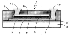
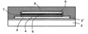
- FIG. 1 is a schematic cross-sectional view showing a first embodiment of a thin film MIM capacitor of the present invention.
- a lower electrode 3 a base metal thin film 4, a dielectric thin film 5 and an upper electrode 6 are sequentially laminated on a substrate 2.
- the base metal thin film 4, the dielectric thin film 5 and the upper electrode 6 are formed in substantially the same area, and the lower electrode 3 has a shape different from that of other thin films in order to form a connection portion with the outside.
- the side surfaces of the base metal thin film 4, the dielectric thin film 5 and the upper electrode 6 are covered with a base metal oxide 7.
- the lower electrode 3, the base metal thin film 4, the dielectric thin film 5, the upper electrode 6 and the base metal oxide 7 are covered with an insulating hydrogen barrier layer 8 and further covered with an insulator 9.
- the upper electrode 6 is connected to the outside by a lead conductor 10
- the lower electrode 3 is connected to the outside by a lead conductor 10 '.
- a SiO 2 layer 2 ′ is formed between the substrate 2 and the lower electrode 3 in order to ensure insulation.
- an insulating substrate such as an alumina substrate is preferably used.
- the SiO 2 layer 2 ′ is formed as described above, but this is not particularly necessary for an insulating substrate such as an alumina substrate.
- the substrate 2 is represented by the size of one component.
- the substrate 2 is actually prepared in the form of a collective substrate so that a plurality of discrete parts can be manufactured at a time and cut and divided later, or is prepared as a part of a multilayer substrate or a substrate of a semiconductor device.
- conductive oxides such as RuO 2 and IrO 2 are preferably used.
- the lower electrode 3 and the upper electrode 6 may use the same material or different materials.
- the lower electrode 3 is etched separately from the upper electrode 6 in order to form a connection portion with the outside.
- the metal thin film to be the lower electrode 3 can be used as an etching stop layer when the base metal thin film 4, the dielectric thin film 5 and the upper electrode 6 are etched together.
- the base metal thin film 4 a base metal having an insulating property by oxidation can be used, but Al, Ti, and Ta are preferably used.
- the base metal thin film 4 functions as a part of the lower electrode.
- the base metal thin film 4 includes the same metal atoms as the base metal oxide 7 covering the side surfaces of the base metal thin film 4, the dielectric thin film 5, and the upper electrode 6.
- the dielectric thin film 5 is abbreviated as barium titanate (BaTiO 3 : hereinafter abbreviated as BT), strontium titanate (SrTiO 3 : hereinafter abbreviated as ST), and barium strontium titanate (BaSrTiO 3 : hereinafter abbreviated as BST). ) Or the like. In particular, BST is preferably used. As the thickness of the dielectric thin film 5 is reduced, the capacitance of the thin film MIM capacitor 1 can be increased.
- the dielectric thin film 5 is formed on the order of nm with a thickness of 1 ⁇ m or less.
- the base metal oxide 7 covers the side surfaces of the base metal thin film 4, the dielectric thin film 5 and the upper electrode 6 as described above.
- the base metal oxide 7 can ensure insulation of the thin film MIM capacitor 1.
- the base metal oxide 7 contains the same metal atoms as the base metal thin film 4. Therefore, it adheres more firmly to the base metal thin film 4, and further adheres more firmly to the side surfaces of the dielectric thin film 5 and the upper electrode 6. Further, when the metal atoms constituting the base metal oxide 7 are Al, Ti, or Ta, the base metal oxide 7 functions as an insulating hydrogen barrier layer.
- the insulating hydrogen barrier layer 8 is formed so that hydrogen generated in the subsequent process of forming the insulator 9 and the process of forming the lead conductor and hydrogen generated when the thin film MIM capacitor 1 is mounted on the electronic circuit or after mounting are formed on the lower electrode. 3. It has a role of preventing entry into the dielectric thin film 5 and the upper electrode 6.
- the insulating hydrogen barrier layer 8 is formed of a material such as Al 2 O 3 , TiO 2 , Ta 2 O 5 , or SiN.
- the insulating layer 9 is formed so as to cover the insulating hydrogen barrier layer 8 as necessary.
- the material of the insulating layer 8 As the material of the insulating layer 8, Al 2 O 3 , SiO 2 or the like is preferably used.
- the lead conductor 10 is connected to the upper electrode 6 through a via hole, and the lead conductor 10 'is connected to the lower electrode 3 through a via hole.
- Cu having a relatively high conductivity is preferably used for the lead conductors 10 and 10 '.
- manufacturing conditions etc. are not limited to the description content of the following description, A various change is possible within the scope of the present invention.
- a substrate 2 is prepared.
- the substrate 2 is a Si substrate.
- an SiO 2 layer 2 ′ is formed.
- the SiO 2 layer 2 ′ is formed in order to improve the insulating property since the insulating property of the Si substrate is relatively low.
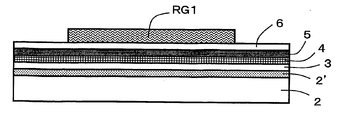
- a substrate 2 is prepared by preparing a Si substrate on which the SiO 2 layer 2 ′ is formed in advance or by oxidizing the surface of the Si substrate to form the SiO 2 layer 2 ′. Subsequently, as shown in FIG. 3, a metal thin film to be the lower electrode 3, a base metal thin film 4, a dielectric thin film 5 and a metal thin film to be the upper electrode 6 are sequentially formed on the entire surface of the substrate 2 on the SiO 2 layer 2 ′. .
- a thin film forming process such as an existing sputtering method, vapor deposition method, CVD method or sol-gel method is used.
- patterning is performed using a photoresist.
- the photoresist either a positive type in which the exposed portion is dissolved and removed, or a negative type in which the exposed portion remains as a pattern may be used.
- Photoresist is applied on the entire surface of the metal thin film to be the upper electrode 6, exposed and developed.
- heat treatment is performed at 100 ° C. to form a patterned resist film RG1.
- the substrate on which the resist film RG1 is formed is placed in a chamber of a dry etching apparatus.
- the temperature in the chamber is set to 200 ° C. or higher so that the thin film particles removed by etching, that is, the etched product, do not reattach to the side surfaces of the thin film MIM capacitor.
- the temperature in the chamber may be room temperature.
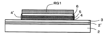
- dry etching is performed to obtain a state as shown in FIG.
- a reactive ion etching method Reactive-Ion-Etching: hereinafter abbreviated as RIE
- RIE reactive ion etching method
- the etched product 4 ′ adheres to the side surface formed by etching.
- This etched product 4 ′ is obtained by reattaching the particles of the base metal thin film 4 removed by the etching.
- the side surface is processed into an inclined surface so that the etched material does not adhere again.
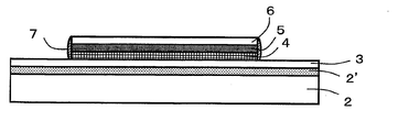
- the RIE method is performed using an ICP (Inductively-Coupled-Plazma) type apparatus. Subsequently, as shown in FIG. 6, the resist film RG ⁇ b> 1 is removed, and the etching product 4 ′ is oxidized to form a base metal oxide 7.
- the etching process 4 ′ can be oxidized simultaneously.
- the etching product 4 ′ is oxidized by annealing. The annealing is performed, for example, in the air or in an oxygen atmosphere at 600 ° C. for 30 minutes. Subsequently, as shown in FIG.
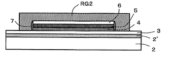
- the base metal thin film 4, the dielectric thin film 5 upper electrode 6 and the base metal oxide 7 are covered with a resist film RG2, and the lower electrode 3 is patterned.
- the patterning method is the same as that for the resist film RG1.
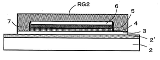
- RIE is performed to remove the portion of the metal thin film that will be the lower electrode 3 that is not covered with the resist film RG2, as shown in FIG.
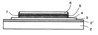
- the resist film RG2 is removed and the lower electrode 3 is formed.
- the method for removing the resist film RG2 is the same as that for the resist film RG1 described above. Note that the oxidation treatment of the etched product 4 ′ may be performed after the resist film RG2 is removed or simultaneously with the removal of the resist film RG2.
- the resist film RG1 is removed with a chemical solution, and then the resist film RG2 is formed without performing the oxidation treatment of the etched product 4 ′, and the lower electrode 3 is patterned. Then, after the resist film RG2 is removed or simultaneously with the removal of the resist film RG2, the etching product 4 ′ is oxidized to form a base metal oxide 7. Subsequently, as shown in FIG. 10, an insulating hydrogen barrier layer 8 is formed.
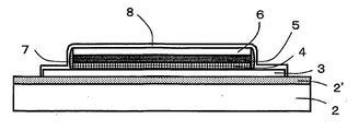
- the insulating hydrogen barrier layer 8 can be formed by an existing thin film formation process. Here, on the side surfaces of the base metal thin film 4, the dielectric thin film 5 and the upper electrode 6, the thickness of the insulating hydrogen barrier layer 8 is formed thinner than the thickness of the insulating hydrogen barrier layer 8 in other portions.
- the base metal oxide 7 exists, it is possible to prevent a decrease in insulation.
- the base metal oxide 7 is an oxide of Al, Ti, or Ta, it is possible to prevent a decrease in hydrogen barrier performance.
- an insulator 9 is formed to cover the entire capacitor portion.
- the insulator 9 can be formed by an existing thin film forming process.
- a via hole VH reaching the upper electrode 6 and a via hole VH ′ reaching the lower electrode 3 are formed.
- the via holes VH and VH ′ can be formed by dry etching.
- a Cu film is formed by electroless Cu plating on the entire surface of the insulator 9 including the via holes VH and VH ′ to form a seed layer (not shown).
- electrolytic Cu plating is performed to deposit Cu on the seed layer.
- excess Cu other than Cu filled in the via holes VH and VH ′ is removed by chemical mechanical polishing (CMP) or the like to form lead conductors 10 and 10 ′.
- CMP chemical mechanical polishing
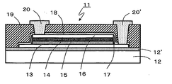
- the base metal oxide thin film 14 oxidizes the base metal thin film 4 of the thin film MIM capacitor 1 shown in FIG. 1 simultaneously with the oxidation treatment of the etched product 4 ′, or forms the base metal oxide thin film from the initial thin film formation. It is formed by the method. In the method of forming the base metal oxide thin film from the time of forming the thin film, no oxidation treatment is required when the base metal oxide 17 is formed.
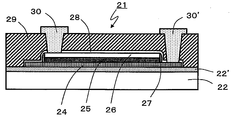
- the thin film MIM capacitor 21 shown in FIG. 14 is different from the thin film MIM capacitor 1 shown in FIG. 1 in that the lower electrode 24 is formed of a base metal thin film.
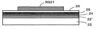
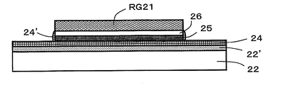
- Such a thin film MIM capacitor 21 is obtained as follows. First, in the manufacturing process of the first embodiment, the process of forming the upper electrode from the lower electrode is changed as shown in FIG. That is, a base metal thin film that becomes the lower electrode 24, a dielectric thin film 25, and a metal thin film that becomes the upper electrode 26 are sequentially formed on the substrate 22 by an existing thin film process. Next, as shown in FIG. 16, a resist film RG21 is formed and patterned. The patterning method is the same as the process of the first embodiment described above. Subsequently, as shown in FIG. 17, a part of the metal thin film to be the upper electrode 26, the dielectric thin film 25, and the base metal thin film to be the lower electrode 24 is collectively etched by RIE.
- an etching product 24 ′ generated by removing a part of the base metal thin film that becomes the lower electrode 24 is reattached to the side surfaces of the dielectric thin film 25 and the upper electrode 26.
- the base metal oxide 27 is formed by oxidizing this etched product 24 '.
Landscapes
- Engineering & Computer Science (AREA)
- Power Engineering (AREA)
- Microelectronics & Electronic Packaging (AREA)
- Manufacturing & Machinery (AREA)
- Chemical & Material Sciences (AREA)
- Materials Engineering (AREA)
- Semiconductor Integrated Circuits (AREA)
- Ceramic Capacitors (AREA)
Abstract
Description
薄膜MIMキャパシタ31は、フォトリソグラフィ技術を用いて、ドライエッチング等の方法で所望の形状に加工される。加工された薄膜MIMキャパシタのキャパシタ部分の側面は、上部電極36および下部電極33がむき出しになっているため、このままでは上部電極36と下部電極33とが短絡しやすい状態にある。そのため、薄膜MIMキャパシタ31は通常絶縁体39によって全体が被覆される。この絶縁体39は薄膜MIMキャパシタ31と同様に薄膜形成プロセスによって形成される。絶縁体39に被覆された薄膜MIMキャパシタは、該絶縁体39を貫通して上部電極36および下部電極33と接続する引出導体40および40’によって静電容量が取り出される。この引出導体40および40’は電解メッキ等の方法で形成される。
しかし、この絶縁体39および引出導体40、40’を形成するときに発生する水素によって、薄膜MIMキャパシタ31の絶縁特性およびリーク電流特性が劣化してしまうことがあった。そのため、薄膜MIMキャパシタ31は絶縁性水素バリア層38が被覆されている。この絶縁性水素バリア層38は、Al2O3、TiO2、Ta2O5、SiNなどの薄膜で構成されている。
本発明は、上記のような課題を解決して、絶縁特性およびリーク電流特性の劣化を防止する効果が充分に得られる薄膜MIMキャパシタを提案するとともに、その薄膜MIMキャパシタを製造する方法を提案するものである。
上記第一の解決手段の薄膜MIMキャパシタは、側面が絶縁体である卑金属酸化物で覆われるため、その上に形成される絶縁性水素バリア層と合わせて充分な絶縁体の厚さを確保することができる。これにより絶縁特性およびリーク電流特性の劣化を防止する効果が充分に得られるようになる。
また、薄膜MIMキャパシタの側面の卑金属酸化物は、薄膜MIMキャパシタを構成する卑金属薄膜または卑金属酸化物薄膜を構成する金属と同じ金属原子を含んでいる。そのため、薄膜MIMキャパシタの側面の卑金属酸化物と、薄膜MIMキャパシタの側面と、の密着が良好になる。
また、本発明では第二の解決手段として上記第一の解決手段に加えて、前記卑金属薄膜または前記卑金属酸化物薄膜を構成する金属がAl、TiまたはTaである薄膜MIMキャパシタを提案する。Al2O3、TiO2、Ta2O5は良好な水素バリア性能を有している。上記第二の解決手段によれば、薄膜MIMキャパシタの側面の卑金属酸化物がAl2O3、TiO2、Ta2O5になるので、薄膜MIMキャパシタの側面における絶縁性水素バリア層の厚さが厚くなる。これにより絶縁特性およびリーク電流特性の劣化を防止する効果がさらに得られるようになる。
なお、上記第一の解決手段において、前記下部電極を卑金属薄膜で形成しても良い。この場合、薄膜MIMキャパシタの側面の卑金属酸化物が下部電極を構成する金属と同じ金属を含むことになるので、薄膜MIMキャパシタの側面の卑金属酸化物と、薄膜MIMキャパシタの側面と、の密着がより良好になる。
また、本発明では第三の解決手段として、上記第一の解決手段で提案された薄膜MIMキャパシタの製造方法において、基板上に、下部電極となる金属膜、卑金属薄膜、誘電体薄膜、および上部電極となる金属膜を順次形成するステップと、前記卑金属薄膜、前記誘電体薄膜、および前記上部電極となる金属膜をドライエッチングによって一括して加工するとともに、前記卑金属薄膜、前記誘電体薄膜および前記上部電極の側面に前記卑金属薄膜のエッチング物を再付着させるステップと、前記エッチング物のみ、または前記エッチング物と前記卑金属薄膜の両方、を酸化処理するステップと、を有する薄膜MIMキャパシタの製造方法を提案する。
上記第三の解決手段によれば、薄膜MIMキャパシタの側面を覆う卑金属酸化物を、ドライエッチングと同時に形成することができる。このため、薄膜MIMキャパシタの側面に絶縁体を形成するためのプロセスを新たに設ける必要がなく、簡易な方法で薄膜MIMキャパシタの側面の絶縁特性およびリーク電流特性を向上させることができる。
薄膜MIMキャパシタ1は、基板2の上に下部電極3、卑金属薄膜4、誘電体薄膜5および上部電極6が順次積層されている。卑金属薄膜4、誘電体薄膜5および上部電極6は略同じ面積に形成されており、下部電極3は外部との接続部分を形成するために他の薄膜と異なる形状となっている。卑金属薄膜4、誘電体薄膜5および上部電極6の側面は卑金属酸化物7で覆われている。下部電極3、卑金属薄膜4、誘電体薄膜5、上部電極6および卑金属酸化物7は絶縁性水素バリア層8で被覆され、さらに絶縁体9で覆われている。上部電極6は引出導体10によって外部と接続され、下部電極3は引出導体10’によって外部と接続される。なお、基板2がSi基板の場合、絶縁性を確保するため、基板2と下部電極3との間にSiO2層2’が形成される。
基板2としては、前述のSi基板のほか、アルミナ基板等の絶縁性基板が好適に用いられる。Si基板の場合には前述のようにSiO2層2’を形成するが、アルミナ基板のような絶縁性基板ではその必要は特にない。なお、以下の説明では、薄膜MIMキャパシタ1を単品のディスクリート部品について説明するため、基板2は部品一個分の大きさで表されている。基板2は実際には、一度に複数のディスクリート部品を製造して後で切断分割できるように集合基板の形で用意されるか、多層基板や半導体装置の基板の一部として用意される。
下部電極3および上部電極6は、Pt、Pd、Au等の貴金属の他、RuO2やIrO2等の導電性酸化物が好適に用いられる。下部電極3と上部電極6は、同じ物質を用いても良いし、異なる物質を用いても良い。下部電極3は外部との接続部分を形成するために、上部電極6とは別々にエッチング加工される。このことを利用して、下部電極3となる金属薄膜を、卑金属薄膜4、誘電体薄膜5および上部電極6を一括してエッチング加工するときのエッチングストップ層とすることもできる。
卑金属薄膜4は、酸化によって絶縁性を有する卑金属が使用可能であるが、Al、Ti、Taが好適に用いられる。卑金属薄膜4はここでは下部電極の一部として機能する。卑金属薄膜4は、卑金属薄膜4、誘電体薄膜5および上部電極6の側面を覆う卑金属酸化物7と同じ金属原子を含んでいる。そのため、卑金属酸化物7との密着性が良い。よって卑金属薄膜4は卑金属酸化物7を卑金属薄膜4、誘電体薄膜5および上部電極6の側面により強固に密着させることができる。
誘電体薄膜5は、チタン酸バリウム(BaTiO3:以下BTと略する。)、チタン酸ストロンチウム(SrTiO3:以下STと略する。)、チタン酸バリウムストロンチウム(BaSrTiO3:以下BSTと略する。)等の誘電体材料で構成されている。特にBSTが好適に用いられる。誘電体薄膜5はその厚さが薄いほど薄膜MIMキャパシタ1の静電容量を大きくすることができる。誘電体薄膜5は、その厚みが1μm以下のnmオーダーで形成される。
卑金属酸化物7は、前述のように卑金属薄膜4、誘電体薄膜5および上部電極6の側面を覆っている。この卑金属酸化物7によって薄膜MIMキャパシタ1の絶縁性を確保することができる。この卑金属酸化物7は、卑金属薄膜4と同じ金属原子を含んでいる。そのため、卑金属薄膜4とより強固に密着し、さらに誘電体薄膜5および上部電極6の側面により強固に密着する。また、卑金属酸化物7を構成する金属原子がAl、Ti、Taであれば、絶縁性水素バリア層としての働きを持つようになる。これによって、卑金属薄膜4、誘電体薄膜5および上部電極6の側面に形成される絶縁性水素バリア層の厚みを厚くすることができる。
絶縁性水素バリア層8は、後工程の絶縁体9の形成工程や引出導体の形成工程にて発生する水素や、薄膜MIMキャパシタ1を電子回路に実装するときあるいは実装後に発生する水素が下部電極3、誘電体薄膜5及び上部電極6に侵入しないようにする役割を有している。絶縁性水素バリア層8は、Al2O3、TiO2、Ta2O5、SiNなどの材料で形成される。
絶縁層9は必要に応じて絶縁性水素バリア層8を覆うように形成される。絶縁層8の材料としてはAl2O3、SiO2等が好適に用いられる。また、引出導体10はビアホールを通して上部電極6と接続され、引出導体10’はビアホールを通して下部電極3と接続される。引出導体10および10’は導電率の比較的高いCuが好適に用いられる。
次に薄膜MIMキャパシタの製造プロセスについて説明する。なお、製造条件等は以下の説明の記載内容に限定されることはなく、本発明の範囲内で種々の変更が可能である。
まず図2に示すように、基板2を用意する。ここで基板2はSi基板とする。基板2上には、SiO2層2’が形成されている。SiO2層2’は、Si基板の絶縁性が比較的低いため、絶縁性を良好にするために形成される。このような基板2は、SiO2層2’が予め形成されたSi基板を用意するか、または、Si基板表面を酸化処理してSiO2層2’を形成することによって用意する。
続いて図3に示すように、基板2のSiO2層2’上の全面に、下部電極3となる金属薄膜、卑金属薄膜4、誘電体薄膜5および上部電極6となる金属薄膜を順次形成する。形成方法としては、既存のスパッタリング法、蒸着法、CVD法あるいはゾルゲル法等の薄膜形成プロセスが用いられる。
続いて図4に示すように、フォトレジストを用いてパターニングを行う。フォトレジストとしては、露光した部分が溶解除去されるポジ型、または露光した部分がパターンとして残るネガ型、のどちらを用いても良い。フォトレジストを上部電極6となる金属薄膜上の全面に塗布し、露光して現像する。次いで100℃で熱処理を行い、パターニングされたレジスト膜RG1を形成する。次にこのレジスト膜RG1を形成した基板をドライエッチング装置のチャンバーに入れる。通常は薄膜MIMキャパシタの側面にエッチングで除去された薄膜の粒子すなわちエッチング物が再付着しないようにチャンバー内の温度を200℃以上に設定する。しかし本発明ではその必要がないので、チャンバー内の温度は常温で良い。
続いてドライエッチングを行い、図5に示すような状態にする。ドライエッチングの方法としては、反応性イオンエッチング法(Reactive−Ion−Etching:以下RIEと略する。)が好適に用いられる。RIEによって上部電極6となる金属薄膜、誘電体薄膜5および卑金属薄膜4を一括してエッチングする。このとき、エッチングによって形成された側面にエッチング物4’が付着する。このエッチング物4’はエッチングによって除去された卑金属薄膜4の粒子が再付着したものである。通常の薄膜MIMキャパシタではエッチング物が再付着しないように側面を傾斜面に加工する。しかし本発明はこのようなエッチング物を敢えて再付着させることを特徴とするものであるため、側面を傾斜面に加工する必要はない。なお、RIEの方法としては、ICP(Inductively−Coupled−Plazma)型の装置を用いて行う。
続いて図6に示すように、レジスト膜RG1を除去し、エッチング物4’を酸化処理して卑金属酸化物7を形成する。レジスト膜RG1は、薬液によって除去する方法の他、酸素プラズマに曝露してアッシング処理によって除去する方法がある。酸素プラズマによるアッシング処理では、エッチング物4’の酸化処理を同時に行うことができる。酸素プラズマによるアッシング処理は、バレル型のアッシング装置を使用し、例えば酸素=100sccm、バイアスパワー240W、圧力100Paの条件で行う。レジスト膜RG1を薬液で除去した場合には、アニールによってエッチング物4’を酸化処理する。アニールは、例えば大気中や酸素雰囲気中で600℃、30分間の条件で行う。
続いて図7に示すように、卑金属薄膜4、誘電体薄膜5上部電極6および卑金属酸化物7をレジスト膜RG2で覆い、下部電極3のパターニングを行う。パターニングの方法は前述のレジスト膜RG1の場合と同様である。続いてRIEを行い、図8に示すように、下部電極3となる金属薄膜の、レジスト膜RG2に覆われていない部分を除去する。続いて図9に示すように、レジスト膜RG2を除去して下部電極3を形成する。レジスト膜RG2を除去する方法は、前述のレジスト膜RG1の場合と同様である。
なお、エッチング物4’の酸化処理は、レジスト膜RG2を除去した後あるいはレジスト膜RG2の除去と同時に行っても良い。すなわち、レジスト膜RG1の除去は薬液で行い、その後エッチング物4’の酸化処理をせずにレジスト膜RG2を形成して下部電極3のパターニングを行う。そしてレジスト膜RG2を除去した後あるいはレジスト膜RG2の除去と同時にエッチング物4’の酸化処理を行い、卑金属酸化物7を形成する。
続いて図10に示すように、絶縁性水素バリア層8を形成する。絶縁性水素バリア層8は、既存の薄膜形成プロセスによって形成することができる。ここで、卑金属薄膜4、誘電体薄膜5および上部電極6の側面において、絶縁性水素バリア層8の厚さが、その他の部分の絶縁性水素バリア層8の厚さよりも薄く形成される。しかし、卑金属酸化物7が存在するので、絶縁性の低下を防止することができる。また、卑金属酸化物7がAl、Ti、Taの酸化物であれば水素バリア性能の低下も防止することができる。
続いて図11に示すように、絶縁体9を形成して、キャパシタ部分全体を被覆する。絶縁体9は、既存の薄膜形成プロセスによって形成することができる。続いて図12に示すように、上部電極6に達するビアホールVHおよび下部電極3に達するビアホールVH’を形成する。ビアホールVHおよびVH’はドライエッチングによって形成することができる。続いてビアホールVHおよびVH’を含む絶縁体9の表面全面に、無電解CuメッキによってCu膜を形成してシード層(図示せず)を形成する。次いで電解Cuメッキを行い、シード層上にCuを析出させる。次いで化学機械研磨(Chemical Mechanical Polishing:CMP)等によってビアホールVHおよびVH’に充填されたCu以外の余分なCuを除去し、引出導体10および10’を形成する。このようにして、図1に示す薄膜MIMキャパシタ1が得られる。
なお、本発明の薄膜MIMキャパシタの第一の実施形態の変形例として、図13に示す薄膜MIMキャパシタ11がある。図1に示す薄膜MIMキャパシタ1と異なる点は、卑金属薄膜4の代わりに卑金属酸化物薄膜14が形成されている点である。この卑金属酸化物薄膜14は、図1に示す薄膜MIMキャパシタ1の卑金属薄膜4を、エッチング物4’の酸化処理の時に同時に酸化するか、あるいは最初の薄膜形成時から卑金属酸化物薄膜を形成するなどの方法で形成される。薄膜形成時から卑金属酸化物薄膜を形成する方法では、卑金属酸化物17を形成するときに酸化処理が不要になる。
次に、本発明の薄膜MIMキャパシタに係る第二の実施形態について説明する。図14に示す薄膜MIMキャパシタ21は、下部電極24が卑金属薄膜で形成されている点が図1に示す薄膜MIMキャパシタ1と異なる。
このような薄膜MIMキャパシタ21は、次のようにして得られる。まず、第一の実施形態の製造プロセスのうち、下部電極から上部電極を形成するプロセスを、図15に示すとおりに変更する。すなわち、基板22上に、下部電極24となる卑金属薄膜、誘電体薄膜25および上部電極26となる金属薄膜を既存の薄膜プロセスによって順次形成する。
次いで図16に示すように、レジスト膜RG21を形成してパターニングを行う。パターニングの方法は前述の第一の実施形態のプロセスと同様である。続いて図17に示すように、上部電極26となる金属薄膜、誘電体薄膜25および下部電極24となる卑金属薄膜の一部をRIEによって一括してエッチング加工する。このとき、下部電極24となる卑金属薄膜の一部が除去されて生じたエッチング物24’が誘電体薄膜25および上部電極26の側面に再付着する。このエッチング物24’を酸化処理することにより、卑金属酸化物27が形成される。
以上、本発明の実施形態について説明したが、本発明は上記実施形態に限定されるものではなく、本発明の範囲内で種々の変更が可能である。
2、12、22、32 基板
2a、12a、22a、32a SiO2層
3、13、33 下部電極
4 卑金属薄膜
4’ エッチング物
5、15、25、35 誘電体薄膜
6、16、26、36 上部電極
7、17、27 卑金属酸化物
8、18、28、38 絶縁性水素バリア層
9、19、29、39 絶縁体
10、10’、20、20’、30、30’、40、40’ 引出導体
14 卑金属酸化物薄膜
24 下部電極(卑金属薄膜)
Claims (5)
- 基板と、該基板上に形成された下部電極と、該下部電極上に形成された誘電体層薄膜と、該誘電体薄膜上に形成された上部電極と、を有する薄膜MIMキャパシタにおいて、
前記下部電極と前記誘電体薄膜との間に、卑金属薄膜または絶縁性の卑金属酸化物薄膜が形成されており、前記誘電体薄膜および前記上部電極の側面が、前記卑金属薄膜または前記卑金属酸化物薄膜を構成する金属と同じ金属原子を含む絶縁性の酸化物で覆われていることを特徴とする薄膜MIMキャパシタ。 - 前記卑金属薄膜または前記卑金属酸化物薄膜を構成する金属がAl、TiまたはTaであることを特徴とする請求項1に記載の薄膜MIMキャパシタ。
- 基板と、該基板上に形成された下部電極と、該下部電極上に形成された誘電体層薄膜と、該誘電体薄膜上に形成された上部電極と、を有する薄膜MIMキャパシタにおいて、前記下部電極は卑金属薄膜で形成されており、前記誘電体薄膜および前記上部電極の側面が、前記下部電極を構成する金属と同じ金属原子を含む絶縁性の酸化物で覆われていることを特徴とする薄膜MIMキャパシタ。
- 基板と、該基板上に形成された下部電極と、該下部電極上に形成された誘電体層薄膜と、該誘電体薄膜上に形成された上部電極と、を有する薄膜MIMキャパシタの製造方法において、
基板上に、下部電極となる金属膜、卑金属薄膜、誘電体薄膜、および上部電極となる金属膜を順次形成するステップと、
前記卑金属薄膜、前記誘電体薄膜、および前記上部電極となる金属膜をドライエッチングによって一括して加工するとともに、前記卑金属薄膜、前記誘電体薄膜および前記上部電極の側面に前記卑金属薄膜のエッチング物を再付着させるステップと、
前記エッチング物のみ、または前記エッチング物と前記卑金属薄膜の両方、を酸化処理するステップと、
を有することを特徴とする薄膜MIMキャパシタの製造方法。 - 基板と、該基板上に形成された下部電極と、該下部電極上に形成された誘電体層薄膜と、該誘電体薄膜上に形成された上部電極と、を有する薄膜MIMキャパシタの製造方法において、
基板上に、下部電極となる卑金属薄膜、誘電体薄膜、および上部電極となる金属膜を順次形成するステップと、
前記卑金属薄膜の一部、前記誘電体薄膜、および前記上部電極となる金属膜をドライエッチングによって一括して加工するとともに、前記誘電体薄膜および前記上部電極の側面に前記卑金属薄膜のエッチング物を再付着させるステップと、
前記エッチング物のみを酸化処理するステップと、
を有することを特徴とする薄膜MIMキャパシタの製造方法。
Priority Applications (2)
| Application Number | Priority Date | Filing Date | Title |
|---|---|---|---|
| CN200980137877.2A CN102165542B (zh) | 2008-10-28 | 2009-10-26 | 薄膜mim电容器及其制造方法 |
| US13/121,081 US8907449B2 (en) | 2008-10-28 | 2009-10-26 | Thin film MIM capacitors and manufacturing method therefor |
Applications Claiming Priority (2)
| Application Number | Priority Date | Filing Date | Title |
|---|---|---|---|
| JP2008-277299 | 2008-10-28 | ||
| JP2008277299A JP5455352B2 (ja) | 2008-10-28 | 2008-10-28 | 薄膜mimキャパシタ及びその製造方法 |
Publications (1)
| Publication Number | Publication Date |
|---|---|
| WO2010050606A1 true WO2010050606A1 (ja) | 2010-05-06 |
Family
ID=42128965
Family Applications (1)
| Application Number | Title | Priority Date | Filing Date |
|---|---|---|---|
| PCT/JP2009/068738 Ceased WO2010050606A1 (ja) | 2008-10-28 | 2009-10-26 | 薄膜mimキャパシタ及びその製造方法 |
Country Status (4)
| Country | Link |
|---|---|
| US (1) | US8907449B2 (ja) |
| JP (1) | JP5455352B2 (ja) |
| CN (1) | CN102165542B (ja) |
| WO (1) | WO2010050606A1 (ja) |
Cited By (1)
| Publication number | Priority date | Publication date | Assignee | Title |
|---|---|---|---|---|
| KR101733608B1 (ko) | 2014-09-18 | 2017-05-10 | 인텔 코포레이션 | 패키지 기판에 매립된 박막 캐패시터의 집적 |
Families Citing this family (21)
| Publication number | Priority date | Publication date | Assignee | Title |
|---|---|---|---|---|
| US9082555B2 (en) | 2011-08-22 | 2015-07-14 | Micron Technology, Inc. | Structure comprising multiple capacitors and methods for forming the structure |
| KR101911127B1 (ko) | 2011-11-09 | 2018-10-23 | 고쿠리츠켄큐카이하츠호진 카가쿠기쥬츠신코키코 | 고체 전자 장치 |
| JP6097540B2 (ja) * | 2012-01-17 | 2017-03-15 | ローム株式会社 | チップコンデンサおよびその製造方法 |
| GB2501872B8 (en) * | 2012-05-03 | 2022-08-17 | Dyson Technology Ltd | Coated Structured Surfaces |
| US9449927B2 (en) * | 2012-11-29 | 2016-09-20 | Taiwan Semiconductor Manufacturing Company, Ltd. | Seal ring structure with metal-insulator-metal capacitor |
| CN104282567B (zh) * | 2013-07-05 | 2017-05-03 | 上海和辉光电有限公司 | 制造igzo层和tft的方法 |
| US9577026B2 (en) * | 2014-05-27 | 2017-02-21 | Taiwan Semiconductor Manufacturing Company Limited | MIM capacitor and method of forming the same |
| CN104200992A (zh) * | 2014-08-29 | 2014-12-10 | 安徽普和电子有限公司 | 一种电容器 |
| US20160181242A1 (en) * | 2014-12-23 | 2016-06-23 | Korea Electronics Technology Institute | Passive device and manufacturing method thereof |
| KR101792381B1 (ko) | 2016-01-04 | 2017-11-01 | 삼성전기주식회사 | 전자부품 및 그 제조방법 |
| WO2018003445A1 (ja) | 2016-06-28 | 2018-01-04 | 株式会社村田製作所 | キャパシタ |
| JP6583220B2 (ja) * | 2016-11-15 | 2019-10-02 | 株式会社村田製作所 | コンデンサ及びコンデンサの製造方法 |
| US9966425B1 (en) | 2017-02-28 | 2018-05-08 | United Microelectronics Corp. | Method for fabricating a MIM capacitor |
| JP6579502B2 (ja) | 2017-07-26 | 2019-09-25 | 株式会社村田製作所 | キャパシタ |
| US10840325B2 (en) * | 2018-04-11 | 2020-11-17 | International Business Machines Corporation | Low resistance metal-insulator-metal capacitor electrode |
| US10861929B2 (en) | 2018-06-27 | 2020-12-08 | Taiwan Semiconductor Manufacturing Co., Ltd. | Electronic device including a capacitor |
| EP3867935A4 (en) | 2018-10-18 | 2022-07-13 | Smoltek AB | DISCREET METAL-INSULATOR-METAL (MIM) ENERGY STORAGE COMPONENT AND METHOD OF FABRICATION |
| TWI691092B (zh) * | 2018-11-05 | 2020-04-11 | 力晶積成電子製造股份有限公司 | 電容單元及其製造方法 |
| WO2021138839A1 (zh) * | 2020-01-08 | 2021-07-15 | 深圳市汇顶科技股份有限公司 | 电容器及其制作方法 |
| CN118692826A (zh) * | 2024-07-05 | 2024-09-24 | 迪盛(武汉)微电子科技有限公司 | 一种薄膜电容器元件及其制造方法 |
| CN121376898A (zh) * | 2025-12-10 | 2026-01-23 | 合肥领航微系统集成有限公司 | 一种叠层式压电mems结构 |
Citations (11)
| Publication number | Priority date | Publication date | Assignee | Title |
|---|---|---|---|---|
| JPH10224756A (ja) | 1997-02-10 | 1998-08-21 | Matsushita Electric Ind Co Ltd | 在宅介護支援システム |
| JP2000150804A (ja) * | 1998-11-05 | 2000-05-30 | Baien Kin | 安定な化学量を有する強誘電体及び/または誘電体の製造方法 |
| JP2001085626A (ja) * | 1999-09-14 | 2001-03-30 | Fuji Electric Co Ltd | 複合電子部品およびその製造方法 |
| JP2001111007A (ja) * | 1999-09-10 | 2001-04-20 | Samsung Electronics Co Ltd | キャパシタ保護膜を含む半導体メモリ素子及びその製造方法 |
| JP2002093797A (ja) * | 2000-06-27 | 2002-03-29 | Samsung Electronics Co Ltd | 絶縁膜を含む集積回路素子の製造方法及びこれによる集積回路素子 |
| JP2002164506A (ja) * | 2000-11-27 | 2002-06-07 | Toshiba Corp | 半導体装置及びその製造方法 |
| JP2002280528A (ja) * | 1999-05-14 | 2002-09-27 | Toshiba Corp | 半導体装置及びその製造方法 |
| JP2003115545A (ja) * | 2001-10-04 | 2003-04-18 | Sony Corp | 誘電体キャパシタおよびその製造方法 |
| JP2006303997A (ja) | 2005-04-21 | 2006-11-02 | Yakichiro Sakai | テレビ会議システム |
| JP2007243017A (ja) * | 2006-03-10 | 2007-09-20 | Toshiba Corp | 半導体装置 |
| JP2008276738A (ja) | 2007-04-30 | 2008-11-13 | Ind Technol Res Inst | 無線周波数識別装置 |
Family Cites Families (7)
| Publication number | Priority date | Publication date | Assignee | Title |
|---|---|---|---|---|
| US6611014B1 (en) | 1999-05-14 | 2003-08-26 | Kabushiki Kaisha Toshiba | Semiconductor device having ferroelectric capacitor and hydrogen barrier film and manufacturing method thereof |
| US7091102B2 (en) * | 2002-12-20 | 2006-08-15 | Samsung Electronics Co., Ltd. | Methods of forming integrated circuit devices having a capacitor with a hydrogen barrier spacer on a sidewall thereof and integrated circuit devices formed thereby |
| JP2004356464A (ja) * | 2003-05-30 | 2004-12-16 | Oki Electric Ind Co Ltd | 強誘電体素子の製造方法、強誘電体素子及びFeRAM |
| JP2006190716A (ja) | 2004-12-28 | 2006-07-20 | Seiko Epson Corp | 強誘電体メモリ素子およびその製造方法 |
| JP2007096178A (ja) * | 2005-09-30 | 2007-04-12 | Toshiba Corp | 半導体装置およびその製造方法 |
| US20080087930A1 (en) * | 2006-10-11 | 2008-04-17 | Jong-Cheol Lee | Capicitor Using Binary Metal Electrode, Semiconductor Device Having The Capacitor And Method of Fabricating The Same |
| US7745280B2 (en) * | 2008-05-29 | 2010-06-29 | United Microelectronics Corp. | Metal-insulator-metal capacitor structure |
-
2008
- 2008-10-28 JP JP2008277299A patent/JP5455352B2/ja not_active Expired - Fee Related
-
2009
- 2009-10-26 CN CN200980137877.2A patent/CN102165542B/zh not_active Expired - Fee Related
- 2009-10-26 US US13/121,081 patent/US8907449B2/en not_active Expired - Fee Related
- 2009-10-26 WO PCT/JP2009/068738 patent/WO2010050606A1/ja not_active Ceased
Patent Citations (11)
| Publication number | Priority date | Publication date | Assignee | Title |
|---|---|---|---|---|
| JPH10224756A (ja) | 1997-02-10 | 1998-08-21 | Matsushita Electric Ind Co Ltd | 在宅介護支援システム |
| JP2000150804A (ja) * | 1998-11-05 | 2000-05-30 | Baien Kin | 安定な化学量を有する強誘電体及び/または誘電体の製造方法 |
| JP2002280528A (ja) * | 1999-05-14 | 2002-09-27 | Toshiba Corp | 半導体装置及びその製造方法 |
| JP2001111007A (ja) * | 1999-09-10 | 2001-04-20 | Samsung Electronics Co Ltd | キャパシタ保護膜を含む半導体メモリ素子及びその製造方法 |
| JP2001085626A (ja) * | 1999-09-14 | 2001-03-30 | Fuji Electric Co Ltd | 複合電子部品およびその製造方法 |
| JP2002093797A (ja) * | 2000-06-27 | 2002-03-29 | Samsung Electronics Co Ltd | 絶縁膜を含む集積回路素子の製造方法及びこれによる集積回路素子 |
| JP2002164506A (ja) * | 2000-11-27 | 2002-06-07 | Toshiba Corp | 半導体装置及びその製造方法 |
| JP2003115545A (ja) * | 2001-10-04 | 2003-04-18 | Sony Corp | 誘電体キャパシタおよびその製造方法 |
| JP2006303997A (ja) | 2005-04-21 | 2006-11-02 | Yakichiro Sakai | テレビ会議システム |
| JP2007243017A (ja) * | 2006-03-10 | 2007-09-20 | Toshiba Corp | 半導体装置 |
| JP2008276738A (ja) | 2007-04-30 | 2008-11-13 | Ind Technol Res Inst | 無線周波数識別装置 |
Cited By (1)
| Publication number | Priority date | Publication date | Assignee | Title |
|---|---|---|---|---|
| KR101733608B1 (ko) | 2014-09-18 | 2017-05-10 | 인텔 코포레이션 | 패키지 기판에 매립된 박막 캐패시터의 집적 |
Also Published As
| Publication number | Publication date |
|---|---|
| CN102165542A (zh) | 2011-08-24 |
| US20110193194A1 (en) | 2011-08-11 |
| JP2010109014A (ja) | 2010-05-13 |
| US8907449B2 (en) | 2014-12-09 |
| JP5455352B2 (ja) | 2014-03-26 |
| CN102165542B (zh) | 2014-04-02 |
Similar Documents
| Publication | Publication Date | Title |
|---|---|---|
| JP5455352B2 (ja) | 薄膜mimキャパシタ及びその製造方法 | |
| JP3966208B2 (ja) | 薄膜キャパシタおよびその製造方法 | |
| JP5344197B2 (ja) | 誘電体薄膜素子及びその製造方法 | |
| JP2008252011A (ja) | 誘電体キャパシタ | |
| JP3995619B2 (ja) | 薄膜キャパシタ素子、その製造方法及び電子装置 | |
| JP4649198B2 (ja) | 配線基板の製造方法 | |
| JP5299158B2 (ja) | 誘電体薄膜素子 | |
| JP2013172075A (ja) | 薄膜素子 | |
| JP4584700B2 (ja) | 配線基板の製造方法 | |
| JP5098422B2 (ja) | 薄膜電子部品 | |
| JP2009010114A (ja) | 誘電体薄膜キャパシタ | |
| JP3362776B2 (ja) | 薄膜コンデンサ、薄膜コンデンサ内蔵基板および薄膜コンデンサの製造方法 | |
| US11430611B2 (en) | Thin film capacitor, circuit board incorporating the same, and thin film capacitor manufacturing method | |
| JP4770627B2 (ja) | キャパシタの製造方法 | |
| JP4770628B2 (ja) | キャパシタの製造方法 | |
| JP2005203680A (ja) | インターポーザキャパシタの製造方法 | |
| US8477474B2 (en) | Thin film capacitor | |
| JP2006005309A (ja) | キャパシタ装置 | |
| JP3838876B2 (ja) | 多層回路基板の製造方法 | |
| JP2004253481A (ja) | 半導体装置およびその製造方法 | |
| JP2003031665A (ja) | 半導体装置の製造方法 | |
| JP2005136074A (ja) | コンデンサおよび直列コンデンサならびに可変コンデンサ | |
| JP5119058B2 (ja) | 薄膜キャパシタ | |
| JP2002008939A (ja) | 選択的コーティングによるセラミック体の製造方法 | |
| JP3987702B2 (ja) | 薄膜コンデンサ |
Legal Events
| Date | Code | Title | Description |
|---|---|---|---|
| WWE | Wipo information: entry into national phase |
Ref document number: 200980137877.2 Country of ref document: CN |
|
| 121 | Ep: the epo has been informed by wipo that ep was designated in this application |
Ref document number: 09823716 Country of ref document: EP Kind code of ref document: A1 |
|
| WWE | Wipo information: entry into national phase |
Ref document number: 13121081 Country of ref document: US |
|
| WWE | Wipo information: entry into national phase |
Ref document number: 2009823716 Country of ref document: EP |
|
| NENP | Non-entry into the national phase |
Ref country code: DE |
|
| 122 | Ep: pct application non-entry in european phase |
Ref document number: 09823716 Country of ref document: EP Kind code of ref document: A1 |