WO2010050476A1 - スイッチング電源装置 - Google Patents
スイッチング電源装置 Download PDFInfo
- Publication number
- WO2010050476A1 WO2010050476A1 PCT/JP2009/068424 JP2009068424W WO2010050476A1 WO 2010050476 A1 WO2010050476 A1 WO 2010050476A1 JP 2009068424 W JP2009068424 W JP 2009068424W WO 2010050476 A1 WO2010050476 A1 WO 2010050476A1
- Authority
- WO
- WIPO (PCT)
- Prior art keywords
- circuit
- series
- switching element
- voltage
- power supply
- Prior art date
- Legal status (The legal status is an assumption and is not a legal conclusion. Google has not performed a legal analysis and makes no representation as to the accuracy of the status listed.)
- Ceased
Links
Images






Classifications
-
- H—ELECTRICITY
- H02—GENERATION; CONVERSION OR DISTRIBUTION OF ELECTRIC POWER
- H02M—APPARATUS FOR CONVERSION BETWEEN AC AND AC, BETWEEN AC AND DC, OR BETWEEN DC AND DC, AND FOR USE WITH MAINS OR SIMILAR POWER SUPPLY SYSTEMS; CONVERSION OF DC OR AC INPUT POWER INTO SURGE OUTPUT POWER; CONTROL OR REGULATION THEREOF
- H02M3/00—Conversion of DC power input into DC power output
- H02M3/22—Conversion of DC power input into DC power output with intermediate conversion into AC
- H02M3/24—Conversion of DC power input into DC power output with intermediate conversion into AC by static converters
- H02M3/28—Conversion of DC power input into DC power output with intermediate conversion into AC by static converters using discharge tubes with control electrode or semiconductor devices with control electrode to produce the intermediate AC
- H02M3/285—Single converters with a plurality of output stages connected in parallel
-
- H—ELECTRICITY
- H02—GENERATION; CONVERSION OR DISTRIBUTION OF ELECTRIC POWER
- H02M—APPARATUS FOR CONVERSION BETWEEN AC AND AC, BETWEEN AC AND DC, OR BETWEEN DC AND DC, AND FOR USE WITH MAINS OR SIMILAR POWER SUPPLY SYSTEMS; CONVERSION OF DC OR AC INPUT POWER INTO SURGE OUTPUT POWER; CONTROL OR REGULATION THEREOF
- H02M1/00—Details of apparatus for conversion
- H02M1/0048—Circuits or arrangements for reducing losses
- H02M1/0054—Transistor switching losses
- H02M1/0058—Transistor switching losses by employing soft switching techniques, i.e. commutation of transistors when applied voltage is zero or when current flow is zero
-
- Y—GENERAL TAGGING OF NEW TECHNOLOGICAL DEVELOPMENTS; GENERAL TAGGING OF CROSS-SECTIONAL TECHNOLOGIES SPANNING OVER SEVERAL SECTIONS OF THE IPC; TECHNICAL SUBJECTS COVERED BY FORMER USPC CROSS-REFERENCE ART COLLECTIONS [XRACs] AND DIGESTS
- Y02—TECHNOLOGIES OR APPLICATIONS FOR MITIGATION OR ADAPTATION AGAINST CLIMATE CHANGE
- Y02B—CLIMATE CHANGE MITIGATION TECHNOLOGIES RELATED TO BUILDINGS, e.g. HOUSING, HOUSE APPLIANCES OR RELATED END-USER APPLICATIONS
- Y02B70/00—Technologies for an efficient end-user side electric power management and consumption
- Y02B70/10—Technologies improving the efficiency by using switched-mode power supplies [SMPS], i.e. efficient power electronics conversion e.g. power factor correction or reduction of losses in power supplies or efficient standby modes
Definitions
- the present invention relates to a simple and inexpensive switching power supply device.
- FIG. 1 is a circuit diagram showing a configuration of a conventional switching power supply device.
- the switching power supply device shown in FIG. 1 is a method called a current resonance type switching power supply device.
- a DC voltage obtained by rectifying and smoothing an AC voltage from a commercial power supply is input as a DC input voltage Vin.
- a switching element Q11 (first switching element) made of a MOSFET and a switching element Q12 (second switching element) made of a MOSFET are connected in series to both ends of a DC power supply Vin that supplies the DC input voltage Vin.
- a voltage resonant capacitor Cv1 is connected between the drain and source of the switching element Q12 (or between the drain and source of the switching element Q11), and the resonant reactor Lr1, the primary winding Np1 of the transformer T1, and the current resonant capacitor Ci1
- the 1st resonance circuit which consists of is connected.
- the resonant reactor Lr1 is substituted by the leakage inductance of the transformer T1, for example.
- a diode D1 is connected between the drain and source of the switching element Q12, and a diode D2 is connected between the drain and source of the switching element Q11.
- Diodes D1 and D2 may be parasitic diodes of switching elements Q11 and Q12.
- secondary windings Ns11 and Ns12 wound in a reverse phase are connected in series to the secondary side of the transformer T1.
- the voltages generated in the secondary windings Ns11 and Ns12 are rectified by the diodes D11 and D12, smoothed by the output smoothing capacitor Co1, and output as the output voltage Vo1.
- a gate signal having a dead time for preventing the switching elements Q11 and Q12 from being simultaneously turned on is alternately input from the control circuit 10 to the gates of the switching elements Q11 and Q12 with the same on width.
- the output voltage Vo1 is fed back to the primary side control circuit 10 through an insulating means such as a photocoupler (not shown), and the switching frequency of the switching elements Q11 and Q12 is controlled by the control circuit 10 so that the output voltage Vo1 becomes a predetermined value. Is done.
- the ripple current Co1i flowing through the output smoothing capacitor Co1 is about 50 to 70% of the output current, which is larger than a forward converter or the like in which current flows continuously.
- An electrolytic capacitor generally used for the output smoothing capacitor Co1 has a specification of an allowable ripple current. In order to satisfy this specification, several electrolytic capacitors must be connected in parallel. For this reason, there existed a subject that cost and a mounting area increased.
- Patent Document 1 discloses a method of reducing a ripple current of an electrolytic capacitor by connecting a plurality of circuits in parallel and operating them by shifting the phases of the respective circuits.
- Patent Document 1 requires a circuit that divides the pulse signal output from the high-frequency oscillation circuit in the control circuit, and has a problem that the control circuit becomes complicated and expensive.
- a first switching element and a second switching element are connected in series at both ends of a DC power source, and auxiliary is provided at both ends of the first switching element or the second switching element.
- a first converter including a first rectifier circuit that rectifies a voltage generated in a secondary winding of the first transformer, wherein a primary winding of a first transformer having a winding and a first capacitor are connected in series;
- a third switching element and a fourth switching element are connected in series to both ends of the DC power supply, and a primary winding and a second capacitor of a second transformer are connected in series to the third switching element or both ends of the fourth switching element.
- a second converter including a second rectifier circuit connected and rectifying a voltage generated in the secondary winding of the second transformer; the first rectifier circuit; and the second rectifier circuit; A smoothing circuit for smoothing the current output from the auxiliary winding, a series resonant circuit composed of a resonant reactor and a resonant capacitor connected in series to the auxiliary winding, and the third switching element according to the current flowing through the series resonant circuit And a control circuit for turning on / off the fourth switching element.
- a first switching element and a second switching element are connected in series to both ends of a direct current power source, and the first switching element or both ends of the second switching element are wound with opposite polarities.
- a primary winding of a first transformer having a first auxiliary winding and a second auxiliary winding and a first capacitor are connected in series, and a first rectification for rectifying a voltage generated in a secondary winding of the first transformer.
- a first converter having a circuit; a third switching element and a fourth switching element connected in series at both ends of the DC power supply; and a primary of a second transformer at both ends of the third switching element or the fourth switching element.
- a second converter including a second rectifier circuit, in which a winding and a second capacitor are connected in series, and rectifies a voltage generated in a secondary winding of the second transformer; and the first rectifier circuit And a first series resonant circuit comprising a first resonant reactor and a first resonant capacitor connected in series to the first auxiliary winding, and a smoothing circuit for smoothing the current output from the second rectifier circuit; A first control circuit for turning on / off the third switching element according to a current of the first series resonance circuit; a second resonance reactor connected in series to the second auxiliary winding; and a second resonance capacitor. And a second control circuit for turning on / off the fourth switching element in accordance with a current of the second series resonance circuit.
- a first switching element and a second switching element are connected in series to both ends of a DC power supply, and a primary winding and a first transformer are connected to both ends of the first switching element or the second switching element.
- a first capacitor having a first rectifier circuit connected to a capacitor in series and rectifying a voltage generated in the secondary winding of the first transformer; a third switching element and a fourth switching element at both ends of the DC power supply; Are connected in series, the primary winding of the second transformer and the second capacitor are connected in series to both ends of the third switching element or the fourth switching element, and the secondary winding of the second transformer
- a second converter comprising a second rectifier circuit for rectifying the generated voltage, a smoothing circuit for smoothing the current output from the first rectifier circuit and the second rectifier circuit,
- a series resonance circuit including a resonance reactor and a resonance capacitor connected to both ends of the first switching element or the second switching element, and the third switching element and the fourth switching element according to a current flowing through the series resonance circuit
- a first switching element and a second switching element are connected in series to both ends of a DC power source, and a primary winding and a first transformer are connected to both ends of the first switching element or the second switching element.
- a third capacitor having a first secondary winding and a second secondary winding that are connected in series with each other and wound in opposite polarities around both ends of the first switching element or the second switching element;
- a transformer primary winding and a third capacitor are connected in series, and a first converter including a first rectifier circuit for rectifying a voltage generated in the secondary winding of the first transformer; 3 switching elements and a fourth switching element are connected in series, and a primary winding and a second capacitor of a second transformer are connected to both ends of the third switching element or the fourth switching element.
- a second converter having a second rectifier circuit connected to the column and rectifying a voltage generated in the secondary winding of the second transformer; and a current output from the first rectifier circuit and the second rectifier circuit.
- a second series resonance circuit and a second control circuit for turning on / off the fourth switching element in accordance with a current of the second series resonance circuit are provided.
- a first power factor correction circuit and a second power factor correction circuit are provided instead of the DC power source,
- the first power factor improving circuit improves the power factor by turning on / off the rectified voltage obtained by rectifying the AC voltage of the AC power source by the first switch, converts the rectified voltage into a predetermined DC voltage, and supplies it to the first converter.
- the second power factor correction circuit improves the power factor by turning on / off the rectified voltage obtained by rectifying the AC voltage by a second switch, and turns on the same as the ON width of the first switch of the first power factor correction circuit. A DC voltage is converted by a width and supplied to the second converter.
- a voltage dividing DC power supply is provided in place of the DC power supply, and the first voltage is applied to both ends of the voltage dividing DC power supply.
- a voltage dividing capacitor and a second voltage dividing capacitor are connected in series, a DC voltage of the first voltage dividing capacitor is supplied to the first converter, and a DC voltage of the second voltage dividing capacitor is supplied to the second converter. It is characterized by being.
- At least one first transformer having a series resonant circuit including a resonant reactor and a resonant capacitor and a winding connected in series to the series resonant circuit, and the first switch circuit is turned on / off.
- a first converter that receives input power from a first DC power source by operation and outputs output power from a secondary side of the first transformer or from a secondary side of another transformer; and a second transformer; A second converter that inputs input power from the first DC power source or the second DC power source by an on / off operation of a switch circuit and outputs output power from a secondary side of the second transformer; the first converter; A rectifying / smoothing circuit that rectifies and smoothes output power output from the second converter and extracts a DC output; and on / off of the second switch circuit according to a current of the series resonance circuit Characterized in that it comprises a control circuit for controlling the work.
- the control circuit turns on / off the switching element of the second converter according to the current of the series resonant circuit composed of the resonant reactor and the resonant capacitor. For this reason, the current discharged from the second converter to the output is a current out of phase with the current output from the first converter. For this reason, a parallel operation with a phase shift can be realized by simply adding a simple circuit, and the ripple current of the output smoothing capacitor can be greatly reduced.
- FIG. 3 is an internal circuit diagram of a control circuit 11 of the switching power supply device according to the first embodiment.
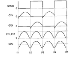
- FIG. 3 is a waveform diagram illustrating an operation of the switching power supply device according to the first embodiment.
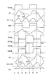
- FIG. 6 is a waveform diagram illustrating an operation of the switching power supply device according to the second embodiment. It is a circuit diagram which shows the structure of the switching power supply device which concerns on Example 3 of this invention.
- FIG. 12 is a circuit diagram of a first modification of the switching power supply device according to the third embodiment.
- FIG. 12 is a circuit diagram of a second modification of the switching power supply device according to the third embodiment. It is a circuit diagram which shows the structure of the switching power supply which concerns on Example 4 of this invention. It is a circuit diagram which shows the structure of the switching power supply device which concerns on Example 5 of this invention. It is a circuit diagram which shows the structure of the switching power supply apparatus which concerns on Example 6 of this invention.
- FIG. 3 is a circuit diagram showing the configuration of the switching power supply apparatus according to Embodiment 1 of the present invention.
- the switching power supply device shown in FIG. 3 includes a DC power supply Vin (first DC power supply), a first converter 3, a second converter 4, and an output smoothing capacitor Co1.
- the first converter 3 is provided with a transformer T1a (first transformer) having a primary winding Np1, secondary windings Ns11 and Ns12, and an auxiliary winding Na1 with respect to the conventional switching power supply device shown in FIG.
- T1a first transformer
- Np1 primary winding
- secondary windings Ns11 and Ns12 secondary windings
- auxiliary winding Na1 auxiliary winding
- the second converter 4 has a switching element Q21 (third switching element) made of MOSFET and a switching element Q22 (fourth switching element) made of MOSFET in series at both ends of the DC power supply Vin. It is connected.
- switching element Q11 and the switching element Q12 constitute a first switch circuit
- switching element Q21 and the switching element Q22 constitute a second switch circuit
- a voltage resonant capacitor Cv2 is connected between the drain and source of the switching element Q22 (or between the drain and source of the switching element Q21), and the resonant reactor Lr2 and the primary winding Np2 of the transformer T2 (second transformer)
- a second resonance circuit composed of a current resonance capacitor Ci2 is connected.
- the resonant reactor Lr2 is substituted by the leakage inductance of the transformer T2, for example.
- a diode D3 is connected between the drain and source of the switching element Q22, and a diode D4 is connected between the drain and source of the switching element Q21.
- Diodes D3 and D4 may be parasitic diodes of switching elements Q21 and Q22.
- secondary windings Ns21 and Ns22 wound in a reverse phase are connected in series to the secondary side of the transformer T2.
- the voltages generated in the secondary windings Ns21 and Ns22 are rectified by the diodes D21 and D22, smoothed by the output smoothing capacitor Co1, and output as the output voltage Vo1.
- the diodes D11, D12, D21, D22 and the output smoothing capacitor Co1 constitute a rectifying / smoothing circuit.
- the control circuit 11 is connected to the gates of the switching elements Q21 and Q22.
- the control circuit 11 is connected to the series resonance circuit 1 (series resonance circuit 1) including a resonance reactor L1 connected to the auxiliary winding Na1 of the transformer T1a and the resonance capacitor C1. Circuit).
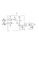
- FIG. 4 is an internal circuit diagram of the control circuit 11 of the switching power supply according to the first embodiment.
- a commutation diode D5 is connected between the base and emitter of the transistor Q1, and a series circuit of the series resonance circuit 1 and the auxiliary winding Na1 of the transformer T1a is connected. Yes.
- the collector of the transistor Q1 is connected to the operating power supply Vcc1 of the control circuit 11 via a resistor R1, for example.
- a driver 14 is connected to the connection point between the collector of the transistor Q1 and the resistor R1, and the output of the driver 14 is connected to the gate of the switching element Q22.
- the inverter circuit 12 is connected to the connection point between the collector of the transistor Q1 and the resistor R1, and the output of the inverter circuit 12 is connected to the gate of the switching element Q21 via the driver 13.
- the driver 13 includes a level shift circuit therein, and converts a signal based on the ground potential into a signal based on a connection point between the switching Q21 and the switching Q22.
- the switching element Q11 and the switching element Q12 are alternately turned on / off with the same on width, and a sinusoidal wave is formed on the secondary side of the transformer T1a. Resonant currents D11i and D12i are released.
- the collector voltage Q1vce of the transistor Q1 is switched in voltage level at an intermediate point (eg, time t2) between the ON periods of the switching elements Q11 and Q12.
- the collector voltage of the transistor Q1 is output through the driver 14 as the gate signal Q22vgs of the switching element Q22. Further, the collector voltage of the transistor Q1 inverted by the inverter circuit 12 is output as the gate signal Q21vgs of the switching element Q21 via the driver 13.
- the drivers 13 and 14 have delay circuits for preventing the switching elements Q21 and Q22 from being turned on simultaneously.
- the second converter 4 When the gate signals Q21vgs and Q22vgs are input to the gates of the switching elements Q21 and Q22, the second converter 4 operates with the same frequency and a phase shift of 90 ° with respect to the first converter 3.
- the resonance time constants of the resonant reactor Lr2 constituting the second resonant circuit, the primary winding Np2 of the transformer T2 and the current resonant capacitor Ci2, and the primary winding Np1 and current of the resonant reactor Lr1 constituting the first resonant circuit and the transformer T1a When the value is the same as the resonance time constant with the resonance capacitor Ci1, the currents D21i and D22i released from the second converter 4 to the output are in phase with the currents D11i and D12i output from the first converter 3. becomes a current shifted 90 °. For this reason, the ripple current Co1i flowing through the output smoothing capacitor Co1 is reduced to about one-fifth as compared with the case where the conventional single converter as shown in FIG. 1 is used.
- the control circuit 11 changes the switching elements Q21 and Q22 of the second converter 4 in accordance with the current L1i of the series resonant circuit 1 including the resonant reactor L1 and the resonant capacitor C1. Turn on / off. That is, only by adding a simple circuit, a parallel operation with a phase shift can be realized, and the ripple current Co1i of the output smoothing capacitor Co1 can be greatly reduced.
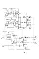
- FIG. 6 is a circuit diagram showing a configuration of a switching power supply apparatus according to Embodiment 2 of the present invention.
- the switching power supply of the second embodiment shown in FIG. 6 differs from the switching power supply of the first embodiment shown in FIG. 3 only in the transformer T1b, the transistors Q1 and Q2, and the diodes D5 and D6. To do.
- the transformer T1b (first transformer) has a primary winding Np1, secondary windings Ns11 and Ns12, and auxiliary windings Nb1 and Nb2.
- the auxiliary winding Nb1 (first auxiliary winding) and the auxiliary winding Nb2 (second auxiliary winding) are wound so as to have opposite phases (reverse polarity).
- a commutation diode D5 is connected between the base and emitter of the transistor Q1 (first control circuit), and a series resonance circuit 1 (first series resonance circuit) including a resonance reactor L1 and a resonance capacitor C1; A series circuit with the auxiliary winding Nb1 of the transformer T1b is connected.
- the emitter of the transistor Q1 is connected to the source of the switching element Q21, and the collector of the transistor Q1 is connected to the gate of the switching element Q21.
- the collector of the transistor Q1 is connected to the operating power supply Vcc2 with reference to the connection point between the switching element Q21 and the switching element Q22 via the resistor R1.
- a commutation diode D6 is connected between the base and emitter of the transistor Q2 (second control circuit), and a series resonance circuit 2 (second series resonance circuit) including a resonance reactor L2 and a resonance capacitor C2; A series circuit with the auxiliary winding Nb2 of the transformer T1b is connected.
- the emitter of the transistor Q2 is connected to the source of the switching element Q22, and the collector of the transistor Q2 is connected to the gate of the switching element Q22.
- the collector of the transistor Q2 is connected to the operating power supply Vcc3 with reference to the ground via a resistor R2.
- the switching element Q11 and the switching element Q12 are alternately turned on / off with the same on width, and a sinusoidal wave is formed on the secondary side of the transformer T1b. Resonant currents D11i and D12i are released.
- the transistors Q1 and Q2 are turned on only during a period in which a positive current is flowing through the series resonant circuits 1 and 2. While the transistors Q1 and Q2 are off, gate signals are input to the switching elements Q21 and Q22 by the resistors R1 and R2.
- the switching elements Q21 and Q22 have the same frequency as the first converter 3a.
- the gate signals Q21vgs and Q22vgs whose phases are shifted by 90 ° are alternately input.
- the ripple current Co1i of the output smoothing capacitor Co1 can be reduced.
- the dead time can be generated by delaying the ON time according to the time constant of the resistors R1 and R2 and the gate capacitances of the switching elements Q21 and Q22, and the delay circuit and the level shift circuit can be eliminated as compared with the first embodiment. .
- FIG. 8 is a circuit diagram showing the configuration of the switching power supply according to Embodiment 3 of the present invention.
- the switching power supply device according to the third embodiment shown in FIG. 8 is different from the switching power supply device according to the second embodiment shown in FIG. 6 in that the transistors Q1 and Q3 (first drive circuit) connected to the totem pole type and the totem pole type connection are used. The difference is that provided transistors Q2 and Q4 (second drive circuit) are provided.
- One end of the series resonant circuit 1 of the resonant reactor L1 and the resonant capacitor C1 is connected to the bases of the transistors Q1 and Q3, and the emitters of the transistors Q1 and Q3 are connected to the gate of the switching element Q21.
- the collector of the transistor Q3 is connected to the source of the switching element Q21, and the collector of the transistor Q1 is connected to the operating power supply Vcc2 via the resistor R1.
- One end of the series resonant circuit 2 of the resonant reactor L2 and the resonant capacitor C2 is connected to the bases of the transistors Q2 and Q4, and the emitters of the transistors Q2 and Q4 are connected to the gate of the switching element Q22.
- the collector of the transistor Q4 is connected to the source of the switching element Q22, and the collector of the transistor Q2 is connected to the operating power supply Vcc3 via the resistor R2.
- the series resonant circuits 1 and 2 receive positive and negative symmetrical triangular wave currents that are 90 ° out of phase with respect to the first converter 3a, and the transistors Q1 and Q3 and the transistors Q2 and Q2, respectively. It flows between the base and emitter of Q4.
- Base current flows through the transistors Q1 and Q2 when the current of the series resonant circuits 1 and 2 is positive, and voltage is applied from the operating power supply Vcc2 and Vcc3 to the gates of the switching elements Q21 and Q22 by the amplification action of the transistors Q1 and Q2.
- the base current flows through the transistors Q3 and Q4 during a period when the current of the series resonant circuits 1 and 2 is negative, and the gate voltages of the switching elements Q21 and Q22 are pulled out by the amplification action of the transistors Q3 and Q4.
- the switching elements Q21 and Q22 are alternately inputted with gate signals having the same frequency and a phase shift of 90 ° with respect to the first converter 3a. Thereby, the ripple current of the output smoothing capacitor Co1 can be reduced as in the first embodiment.
- the input signal to the totem pole type drive circuit is not a voltage source but a current source from the series resonance circuits 1 and 2, the current of the series resonance circuits 1 and 2 is Even if the current is inverted, the transistor cannot be turned off until the current value reaches the minority carrier charge amount accumulated in the base of the transistor, and a delay time is generated with respect to switching of the current direction.
- FIG. 9 is a circuit diagram of a first modification of the switching power supply according to the third embodiment.
- the delay time of the drive circuit is eliminated.
- the first modification of FIG. 9 differs from the third embodiment shown in FIG. 8 only in the drive circuit, and therefore, description of other common parts is omitted.
- diodes D7 and D8 having a low forward voltage drop are added between the collectors and bases of the transistors Q1 and Q3. Although not shown, diodes are similarly added to the transistors Q2 and Q4.
- FIG. 10 is a circuit diagram of a second modification of the switching power supply according to the third embodiment.
- the second modification shown in FIG. 10 adds diodes D9 and D10 (second diodes) between the series resonance circuit 1 and the bases of the transistors Q1 and Q3 with respect to the first modification shown in FIG.
- a resistor R3 is added between the base and emitter of the transistor Q1.
- diodes and resistors are similarly added to the transistors Q2 and Q4.
- the delay time can be shortened in the same way as the drive circuit shown in FIG. Further, when the current of the series resonant circuits 1 and 2 switches from negative to positive, initially, the current flows through the resistor R3, so that the transistor Q1 is not immediately turned on. The base current flows after the voltage drop of the resistor R3 reaches the base-emitter voltage of the transistor Q1, and the transistor Q1 is turned on. Therefore, the timing at which the switching elements Q21 and Q22 are switched from OFF to ON, that is, the dead time can be adjusted by the resistance values of the resistors R1 and R2.
- FIG. 11 is a circuit diagram showing a configuration of a switching power supply apparatus according to Embodiment 4 of the present invention.
- the series resonant circuits 1 and 2 are connected to the auxiliary windings Nb1 and Nb2 of the transformer T1b.
- Example 4 shown in FIG. 11 a transformer T3 (first transformer) having a primary winding Np3 and secondary windings Ns31 and Ns32 is provided, and one end of the secondary winding Ns31 of the transformer T3 is provided.
- One end of the series resonance circuit 1 is connected, and one end of the series resonance circuit 2 is connected to one end of the secondary winding Ns32 of the transformer T3.
- a series circuit of a capacitor C3 and a primary winding Np3 of the transformer T3 is connected to both ends of the switching element Q12.
- the transformer T1 constitutes another transformer.
- the first and second converters have resonant capacitors Lr1 and Lr2, primary windings Np1 and Np2 of transformers T1a and T2, and resonant operations of the first resonant circuit and the second resonant circuit by the current resonant capacitors Ci1 and Ci2, respectively.
- Ci1 and Ci2 are amplified, and the voltages are generated in the secondary windings Ns11, Ns12, Ns21, and Ns22 to transmit energy.
- the voltages generated in the secondary windings Ns11, Ns12, Ns21, and Ns22 of the transformers T1a and T2 are large due to variations in the resonance reactors Lr1 and Lr2, the inductance of the primary winding, the capacitance of the current resonance capacitors Ci1 and Ci2, and the like. May be different. Since the secondary side of the transformers T1a and T2 does not control the current between the rectifier diodes D11, D12, D21, and D22 and the output smoothing capacitor Co1, the side where the secondary winding voltage is low is the secondary winding voltage. Becomes a voltage lower than the voltage of the output smoothing capacitor Co1.
- rectifier diodes D11 and D12 or D21 and D22 are not conducted, and power is supplied by only one of the two converters 3 and 4. That is, originally, the power supplied by the two converters 3 and 4 is carried by one converter, and there is a risk of heat generation of each switching element.
- FIG. 12 is a circuit diagram showing a configuration of a switching power supply apparatus according to Embodiment 5 of the present invention.
- the switching power supply device according to the fifth embodiment shown in FIG. 12 replaces the direct current power supply Vin of the switching power supply device according to the fourth embodiment shown in FIG.
- a first PFC circuit 23 (first power factor correction circuit) including an element Q31 (first switch), a diode D31, and a capacitor C31 (first DC power supply), a switching element Q41 (second switch) including a boost reactor L41 and a MOSFET
- the second PFC circuit 24 (second power factor correction circuit) including the diode D41 and the capacitor C41 (second DC power supply) and the control circuit 15 are provided.
- the first PFC circuit 23 is connected to both ends of a series circuit of the switching element Q11 and the switching element Q12.
- the first PFC circuit 23 uses a rectified voltage obtained by rectifying the AC voltage of the AC power supply AC by the full-wave rectifier circuit DB. It is turned on / off by control to improve the power factor and convert it to a predetermined DC voltage.
- the second PFC circuit 24 is connected to both ends of the series circuit of the switching element Q21 and the switching element Q22, and the rectified voltage obtained by rectifying the AC voltage of the AC power supply AC by the full-wave rectifier circuit DB is used. It is turned on / off by control to improve the power factor, and is converted to a DC voltage with the same ON width as the ON width of the first PFC circuit 23.
- the two PFC circuits 23 and 24 are controlled by one control circuit 15. That is, only the output voltage of the first PFC circuit 23 connected to the first converter 3b is controlled by the control circuit 15, the output voltage of the second PFC circuit 24 is not monitored, and the ON width of the first PFC circuit 23 that is voltage controlled. It is operated with the same ON width (ON width of switching element Q41) as (ON width of switching element Q31).
- the output voltage of the second PFC circuit 24 is lower than the output voltage of the first PFC circuit 23.
- the output voltage of the second PFC circuit 24 becomes higher than the output voltage of the first PFC circuit 23.
- the voltage of the current resonance capacitor Ci2 changes, and the voltage generated in the secondary windings Ns21 and Ns22 of the transformer T2 changes.
- the output voltage of the second PFC circuit 24 decreases, and the voltages generated in the secondary windings Ns21 and Ns22 of the transformer T2 together. Decreases, and the power output from the second converter 4 decreases. For this reason, it becomes a stable operation when the power output from the first converter 3b and the second converter 4 is balanced. That is, the current balance of the two converters 3b and 4 can be realized by adding only the PFC circuits 23 and 24 without performing complicated control.
- FIG. 13 is a circuit diagram showing a configuration of a switching power supply apparatus according to Embodiment 6 of the present invention.
- a voltage dividing capacitor C33 first voltage dividing capacitor, first DC power supply
- a voltage dividing capacitor C43 second voltage dividing capacitor, second DC power supply
- the series circuit of the switching element Q11 and the switching element Q12 is connected to both ends of the voltage dividing capacitor C33, and the series circuit of the switching element Q21 and the switching element Q22 is connected to both ends of the voltage dividing capacitor C43.
- the voltage across the voltage dividing capacitors C33 and C43 is a voltage obtained by dividing the DC voltage of the DC power supply Vin in half.
- the input voltage of the second converter 4 decreases, the voltage generated in the secondary windings Ns21 and Ns22 of the transformer T2 decreases, and the power output from the second converter 4 decreases. For this reason, it becomes a stable operation when the power output from the first converter 3b and the second converter 4 is balanced.
- the voltage across the voltage dividing capacitor C43 rises compared to the voltage across the voltage dividing capacitor C33. That is, the input voltage of the second converter 4 rises, the voltage generated in the secondary windings Ns21 and Ns22 of the transformer T2 rises, and the power output from the second converter 4 increases. For this reason, it becomes a stable operation when the power output from the first converter 3b and the second converter 4 is balanced. That is, the current balance between the two converters 3b and 4 can be realized with a simple configuration.
- this invention is not limited to the Example mentioned above.
- the current resonance type switching power supply device is illustrated, but the present invention can also be applied to a push-pull type switching power supply device.
- first PFC circuit 23 and the second PFC circuit 24 of the switching power supply device of the fifth embodiment shown in FIG. 12 may be applied to any of the switching power supply devices of the first to third embodiments.
- the voltage dividing capacitor C33 and the voltage dividing capacitor C43 of the switching power supply device of the sixth embodiment shown in FIG. 13 may be applied to any one of the switching power supply devices of the first to third embodiments.
Landscapes
- Engineering & Computer Science (AREA)
- Power Engineering (AREA)
- Dc-Dc Converters (AREA)
- Rectifiers (AREA)
Abstract
Description
3,3a,3b 第1コンバータ
4 第2コンバータ
10,11,15 制御回路
12 インバータ回路
13,14 ドライバ
23 第1PFC回路
24 第2PFC回路
Vin 直流電源
Q11,Q12,Q21,Q22,Q31,Q41 スイッチング素子
Q1~Q4 トランジスタ
D1~D12,D21,D22,D31,D41 ダイオード
T1,T1a,T1b,T2,T3 トランス
Np1,Np2,Np3 一次巻線
Ns11,Ns12,Ns21,Ns22,Ns31,Ns32 二次巻線
Na1,Nb1,Nb2 補助巻線
C33,C43 分圧コンデンサ
Co1 出力平滑コンデンサ
L31,L41 昇圧リアクトル
Lr1,Lr2,L1,L2 共振リアクトル
C1,C2 共振コンデンサ
Ci1,Ci2 電流共振コンデンサ
Cv1,Cv2 電圧共振コンデンサ
R1,R2 抵抗
AC 交流電源
DB 全波整流回路
Claims (17)
- 直流電源の両端に第1スイッチング素子と第2スイッチング素子とが直列に接続され、前記第1スイッチング素子又は前記第2スイッチング素子の両端に補助巻線を有する第1トランスの一次巻線と第1コンデンサとが直列に接続され、前記第1トランスの二次巻線に発生した電圧を整流する第1整流回路を備える第1コンバータと、
前記直流電源の両端に第3スイッチング素子と第4スイッチング素子とが直列に接続され、前記第3スイッチング素子又は前記第4スイッチング素子の両端に第2トランスの一次巻線と第2コンデンサとが直列に接続され、前記第2トランスの二次巻線に発生した電圧を整流する第2整流回路を備える第2コンバータと、
前記第1整流回路と前記第2整流回路とから出力される電流を平滑する平滑回路と、
前記補助巻線に直列に接続された共振リアクトルと共振コンデンサとからなる直列共振回路と、
前記直列共振回路に流れる電流に応じて前記第3スイッチング素子及び前記第4スイッチング素子をオン/オフさせる制御回路と、
を備えることを特徴とするスイッチング電源装置。 - 前記制御回路は、前記直列共振回路に流れる電流が正のときに前記第3スイッチング素子をオンさせ、前記直列共振回路に流れる電流が負のときに前記第4スイッチング素子をオンさせることを特徴とする請求項1記載のスイッチング電源装置。
- 直流電源の両端に第1スイッチング素子と第2スイッチング素子とが直列に接続され、前記第1スイッチング素子又は前記第2スイッチング素子の両端に互いに逆極性に巻回された第1補助巻線と第2補助巻線とを有する第1トランスの一次巻線と第1コンデンサとが直列に接続され、前記第1トランスの二次巻線に発生した電圧を整流する第1整流回路を備える第1コンバータと、
前記直流電源の両端に第3スイッチング素子と前記第4スイッチング素子とが直列に接続され、前記第3スイッチング素子又は前記第4スイッチング素子の両端に第2トランスの一次巻線と第2コンデンサとが直列に接続され、前記第2トランスの二次巻線に発生した電圧を整流する第2整流回路を備える第2コンバータと、
前記第1整流回路と前記第2整流回路とから出力される電流を平滑する平滑回路と、
前記第1補助巻線に直列に接続された第1共振リアクトルと第1共振コンデンサとからなる第1直列共振回路と、
前記第1直列共振回路の電流に応じて前記第3スイッチング素子をオン/オフさせる第1制御回路と、
前記第2補助巻線に直列に接続された第2共振リアクトルと第2共振コンデンサとからなる第2直列共振回路と、
前記第2直列共振回路の電流に応じて前記第4スイッチング素子をオン/オフさせる第2制御回路と、
を備えることを特徴とするスイッチング電源装置。 - 前記第1制御回路は、トーテムポール接続された第1及び第2トランジスタを有し、前記第1及び第2トランジスタの各ベース端子が前記第1直列共振回路と前記第1補助巻線とからなる直列回路の一端に接続され、各エミッタ端子が前記第1直列共振回路と前記第1補助巻線とからなる直列回路の他端と前記第3スイッチング素子の制御端子とに接続された第1ドライブ回路を備え、
前記第2制御回路は、トーテムポール接続された第3及び第4トランジスタを有し、前記第3及び第4トランジスタの各ベース端子が前記第2直列共振回路と前記第2補助巻線とからなる直列回路の一端に接続され、各エミッタ端子が前記第2直列共振回路と前記第2補助巻線とからなる直列回路の他端と前記第4スイッチング素子の制御端子とに接続された第2ドライブ回路を備えることを特徴とする請求項3記載のスイッチング電源装置。 - 前記第1ドライブ回路及び前記第2ドライブ回路の各々は、各トランジスタについてベース端子とコレクタ端子との間に接続されたダイオードを備えることを特徴とする請求項4記載のスイッチング電源装置。
- 前記第1制御回路は、トーテムポール接続された第1及び第2トランジスタを有し、前記第1及び第2トランジスタの各ベース端子及び各コレクタ端子がそれぞれにダイオードを介して前記第1直列共振回路と前記第1補助巻線とからなる直列回路の一端に接続され、各エミッタ端子が前記第1直列共振回路と前記第1補助巻線とからなる直列回路の他端と前記第3スイッチング素子の制御端子とに接続され、前記第1トランジスタのベース端子及びエミッタ端子間に抵抗が接続された第1ドライブ回路を備え、
前記第2制御回路は、トーテムポール接続された第3及び第4トランジスタを有し、前記第3及び第4トランジスタの各ベース端子及び各コレクタ端子がそれぞれにダイオードを介して前記第2直列共振回路と前記第2補助巻線とからなる直列回路の一端に接続され、各エミッタ端子が前記第2直列共振回路と前記第2補助巻線とからなる直列回路の他端と前記第4スイッチング素子の制御端子とに接続され、前記第3トランジスタのベース端子及びエミッタ端子間に抵抗が接続された第2ドライブ回路を備えることを特徴とする請求項3記載のスイッチング電源装置。 - 直流電源の両端に第1スイッチング素子と第2スイッチング素子とが直列に接続され、前記第1スイッチング素子又は前記第2スイッチング素子の両端に第1トランスの一次巻線と第1コンデンサとが直列に接続され、前記第1トランスの二次巻線に発生した電圧を整流する第1整流回路を備える第1コンバータと、
前記直流電源の両端に第3スイッチング素子と第4スイッチング素子とが直列に接続され、前記第3スイッチング素子又は前記第4スイッチング素子の両端に第2トランスの一次巻線と第2コンデンサとが直列に接続され、前記第2トランスの二次巻線に発生した電圧を整流する第2整流回路を備える第2コンバータと、
前記第1整流回路と前記第2整流回路とから出力される電流を平滑する平滑回路と、
前記第1スイッチング素子又は前記第2スイッチング素子の両端に接続された共振リアクトルと共振コンデンサとからなる直列共振回路と、
前記直列共振回路に流れる電流に応じて前記第3スイッチング素子及び前記第4スイッチング素子をオン/オフさせる制御回路と、
を備えることを特徴とするスイッチング電源装置。 - 直流電源の両端に第1スイッチング素子と第2スイッチング素子とが直列に接続され、前記第1スイッチング素子又は前記第2スイッチング素子の両端に第1トランスの一次巻線と第1コンデンサとが直列に接続され、前記第1スイッチング素子又は前記第2スイッチング素子の両端に互いに逆極性に巻回された第1の二次巻線及び第2の二次巻線を有する第3トランスの一次巻線と第3コンデンサとが直列に接続され、前記第1トランスの二次巻線に発生した電圧を整流する第1整流回路を備える第1コンバータと、
前記直流電源の両端に第3スイッチング素子と第4スイッチング素子とが直列に接続され、前記第3スイッチング素子又は前記第4スイッチング素子の両端に第2トランスの一次巻線と第2コンデンサとが直列に接続され、前記第2トランスの二次巻線に発生した電圧を整流する第2整流回路を備える第2コンバータと、
前記第1整流回路と前記第2整流回路とから出力される電流を平滑する平滑回路と、
前記第3トランスの第1の二次巻線に直列に接続された第1共振リアクトルと第1共振コンデンサとからなる第1直列共振回路と、
前記第1直列共振回路の電流に応じて前記第3スイッチング素子をオン/オフさせる第1制御回路と、
前記第3トランスの第2の二次巻線に直列に接続された第2共振リアクトルと第2共振コンデンサとからなる第2直列共振回路と、
前記第2直列共振回路の電流に応じて前記第4スイッチング素子をオン/オフさせる第2制御回路と、
を備えることを特徴とするスイッチング電源装置。 - 前記直流電源に代えて、第1力率改善回路と第2力率改善回路とを設け、
前記第1力率改善回路は、交流電源の交流電圧を整流した整流電圧を第1スイッチによりオン/オフして力率を改善するとともに所定の直流電圧に変換して前記第1コンバータに供給し、
前記第2力率改善回路は、前記交流電圧を整流した整流電圧を第2スイッチによりオン/オフして力率を改善するとともに前記第1力率改善回路の第1スイッチのオン幅と同じオン幅で直流電圧に変換して前記第2コンバータに供給することを特徴とする請求項1記載のスイッチング電源装置。 - 前記直流電源に代えて、第1力率改善回路と第2力率改善回路とを設け、
前記第1力率改善回路は、交流電源の交流電圧を整流した整流電圧を第1スイッチによりオン/オフして力率を改善するとともに所定の直流電圧に変換して前記第1コンバータに供給し、
前記第2力率改善回路は、前記交流電圧を整流した整流電圧を第2スイッチによりオン/オフして力率を改善するとともに前記第1力率改善回路の第1スイッチのオン幅と同じオン幅で直流電圧に変換して前記第2コンバータに供給することを特徴とする請求項3記載のスイッチング電源装置。 - 前記直流電源に代えて、第1力率改善回路と第2力率改善回路とを設け、
前記第1力率改善回路は、交流電源の交流電圧を整流した整流電圧を第1スイッチによりオン/オフして力率を改善するとともに所定の直流電圧に変換して前記第1コンバータに供給し、
前記第2力率改善回路は、前記交流電圧を整流した整流電圧を第2スイッチによりオン/オフして力率を改善するとともに前記第1力率改善回路の第1スイッチのオン幅と同じオン幅で直流電圧に変換して前記第2コンバータに供給することを特徴とする請求項7記載のスイッチング電源装置。 - 前記直流電源に代えて、第1力率改善回路と第2力率改善回路とを設け、
前記第1力率改善回路は、交流電源の交流電圧を整流した整流電圧を第1スイッチによりオン/オフして力率を改善するとともに所定の直流電圧に変換して前記第1コンバータに供給し、
前記第2力率改善回路は、前記交流電圧を整流した整流電圧を第2スイッチによりオン/オフして力率を改善するとともに前記第1力率改善回路の第1スイッチのオン幅と同じオン幅で直流電圧に変換して前記第2コンバータに供給することを特徴とする請求項8記載のスイッチング電源装置。 - 前記直流電源に代えて、分圧用直流電源を設けるとともに、前記分圧用直流電源の両端に第1分圧コンデンサと第2分圧コンデンサとが直列に接続され、前記第1分圧コンデンサの直流電圧が前記第1コンバータに供給され、前記第2分圧コンデンサの直流電圧が前記第2コンバータに供給されることを特徴とする請求項1記載のスイッチング電源装置。
- 前記直流電源に代えて、分圧用直流電源を設けるとともに、前記分圧用直流電源の両端に第1分圧コンデンサと第2分圧コンデンサとが直列に接続され、前記第1分圧コンデンサの直流電圧が前記第1コンバータに供給され、前記第2分圧コンデンサの直流電圧が前記第2コンバータに供給されることを特徴とする請求項3記載のスイッチング電源装置。
- 前記直流電源に代えて、分圧用直流電源を設けるとともに、前記分圧用直流電源の両端に第1分圧コンデンサと第2分圧コンデンサとが直列に接続され、前記第1分圧コンデンサの直流電圧が前記第1コンバータに供給され、前記第2分圧コンデンサの直流電圧が前記第2コンバータに供給されることを特徴とする請求項7記載のスイッチング電源装置。
- 前記直流電源に代えて、分圧用直流電源を設けるとともに、前記分圧用直流電源の両端に第1分圧コンデンサと第2分圧コンデンサとが直列に接続され、前記第1分圧コンデンサの直流電圧が前記第1コンバータに供給され、前記第2分圧コンデンサの直流電圧が前記第2コンバータに供給されることを特徴とする請求項8記載のスイッチング電源装置。
- 共振リアクトルと共振コンデンサとからなる直列共振回路と、
前記直列共振回路に直列に接続される巻線を有する第1トランスを少なくとも1つ備え、第1スイッチ回路のオン/オフ動作により第1直流電源から入力電力を入力し、前記第1トランスの二次側から、又は他のトランスの二次側から出力電力を出力する第1コンバータと、
第2トランスを備え、第2スイッチ回路のオン/オフ動作により前記第1直流電源又は第2直流電源から入力電力を入力し、前記第2トランスの二次側から出力電力を出力する第2コンバータと、
前記第1コンバータと前記第2コンバータとから出力される出力電力を整流平滑して直流出力を取り出す整流平滑回路と、
前記直列共振回路の電流に応じて前記第2スイッチ回路のオン/オフ動作を制御する制御回路と、
を備えることを特徴とするスイッチング電源装置。
Priority Applications (3)
| Application Number | Priority Date | Filing Date | Title |
|---|---|---|---|
| KR1020107023942A KR101203918B1 (ko) | 2008-10-30 | 2009-10-27 | 스위칭 전원 장치 |
| US12/990,390 US8542501B2 (en) | 2008-10-30 | 2009-10-27 | Switching power-supply apparatus |
| CN2009801154023A CN102017379B (zh) | 2008-10-30 | 2009-10-27 | 开关电源装置 |
Applications Claiming Priority (2)
| Application Number | Priority Date | Filing Date | Title |
|---|---|---|---|
| JP2008-279867 | 2008-10-30 | ||
| JP2008279867A JP4525817B2 (ja) | 2008-10-30 | 2008-10-30 | スイッチング電源装置 |
Publications (1)
| Publication Number | Publication Date |
|---|---|
| WO2010050476A1 true WO2010050476A1 (ja) | 2010-05-06 |
Family
ID=42128837
Family Applications (1)
| Application Number | Title | Priority Date | Filing Date |
|---|---|---|---|
| PCT/JP2009/068424 Ceased WO2010050476A1 (ja) | 2008-10-30 | 2009-10-27 | スイッチング電源装置 |
Country Status (6)
| Country | Link |
|---|---|
| US (1) | US8542501B2 (ja) |
| JP (1) | JP4525817B2 (ja) |
| KR (1) | KR101203918B1 (ja) |
| CN (1) | CN102017379B (ja) |
| TW (1) | TWI443945B (ja) |
| WO (1) | WO2010050476A1 (ja) |
Cited By (2)
| Publication number | Priority date | Publication date | Assignee | Title |
|---|---|---|---|---|
| WO2012000432A1 (zh) * | 2010-07-01 | 2012-01-05 | 浙江昱能光伏科技集成有限公司 | 轮替主从分路的交错并联反激变换器 |
| WO2020010609A1 (en) * | 2018-07-13 | 2020-01-16 | Tridonic Gmbh & Co Kg | Power supply circuit, controlling method and electric equipment |
Families Citing this family (55)
| Publication number | Priority date | Publication date | Assignee | Title |
|---|---|---|---|---|
| JP5282424B2 (ja) * | 2008-03-14 | 2013-09-04 | ダイキン工業株式会社 | 整流回路 |
| US10172669B2 (en) | 2009-10-09 | 2019-01-08 | Ethicon Llc | Surgical instrument comprising an energy trigger lockout |
| CN102792576B (zh) * | 2010-03-16 | 2015-06-24 | 株式会社村田制作所 | 开关电源装置 |
| GB2480498A (en) | 2010-05-21 | 2011-11-23 | Ethicon Endo Surgery Inc | Medical device comprising RF circuitry |
| JP5659575B2 (ja) * | 2010-06-22 | 2015-01-28 | 株式会社リコー | マルチフェーズ型コンバータ |
| CN102545607A (zh) * | 2010-12-21 | 2012-07-04 | 鸿富锦精密工业(深圳)有限公司 | 电压调节系统 |
| GB2486509B (en) | 2011-03-22 | 2013-01-09 | Enecsys Ltd | Solar photovoltaic power conditioning units |
| JP2013005547A (ja) | 2011-06-15 | 2013-01-07 | Sanken Electric Co Ltd | スイッチング電源装置 |
| JP5768886B2 (ja) * | 2011-08-04 | 2015-08-26 | 株式会社村田製作所 | スイッチング電源装置 |
| US8760893B2 (en) * | 2011-10-07 | 2014-06-24 | Rohm Co., Ltd. | Full bridge switching circuit |
| US9421060B2 (en) | 2011-10-24 | 2016-08-23 | Ethicon Endo-Surgery, Llc | Litz wire battery powered device |
| JP5873293B2 (ja) * | 2011-10-31 | 2016-03-01 | キヤノン株式会社 | 電源装置および画像形成装置 |
| CN102570862A (zh) * | 2012-02-15 | 2012-07-11 | 杭州矽力杰半导体技术有限公司 | 一种具有多路输出的电流平衡电路 |
| WO2013132727A1 (ja) * | 2012-03-05 | 2013-09-12 | 富士電機株式会社 | 直流-直流変換装置 |
| WO2013146338A1 (ja) * | 2012-03-30 | 2013-10-03 | 株式会社村田製作所 | スイッチング電源装置 |
| KR101405789B1 (ko) * | 2012-12-04 | 2014-06-12 | 주식회사 만도 | 전동 파워 스티어링 릴레이의 직류 링크 커패시터 충전-방전 제어장치 및 그 방법 |
| JP2014241707A (ja) * | 2013-06-12 | 2014-12-25 | トヨタ自動車株式会社 | 電源装置及びその制御方法 |
| US10020747B2 (en) | 2014-04-15 | 2018-07-10 | Danmarks Tekniske Universitet | Resonant DC-DC power converter assembly |
| US10159524B2 (en) | 2014-12-22 | 2018-12-25 | Ethicon Llc | High power battery powered RF amplifier topology |
| CN106160206A (zh) * | 2015-03-31 | 2016-11-23 | 通用电气公司 | 电源系统及能量存储系统 |
| US9847710B2 (en) * | 2015-04-02 | 2017-12-19 | Virginia Tech Intellectual Properties, Inc. | Universal system structure for low power adapters |
| US10314638B2 (en) | 2015-04-07 | 2019-06-11 | Ethicon Llc | Articulating radio frequency (RF) tissue seal with articulating state sensing |
| JP6573502B2 (ja) * | 2015-08-07 | 2019-09-11 | 新電元工業株式会社 | Dc−dcコンバータ |
| US10491123B2 (en) * | 2015-09-18 | 2019-11-26 | Murata Manufacturing Co., Ltd. | Modular parallel technique for resonant converter |
| US10959771B2 (en) | 2015-10-16 | 2021-03-30 | Ethicon Llc | Suction and irrigation sealing grasper |
| US9601904B1 (en) * | 2015-12-07 | 2017-03-21 | Raytheon Company | Laser diode driver with variable input voltage and variable diode string voltage |
| US10959806B2 (en) | 2015-12-30 | 2021-03-30 | Ethicon Llc | Energized medical device with reusable handle |
| US10856934B2 (en) | 2016-04-29 | 2020-12-08 | Ethicon Llc | Electrosurgical instrument with electrically conductive gap setting and tissue engaging members |
| US10987156B2 (en) | 2016-04-29 | 2021-04-27 | Ethicon Llc | Electrosurgical instrument with electrically conductive gap setting member and electrically insulative tissue engaging members |
| WO2018026133A1 (ko) * | 2016-08-05 | 2018-02-08 | 삼성전자 주식회사 | 스위칭 장치 및 전력 변환 장치 |
| RU2628211C1 (ru) | 2016-08-05 | 2017-08-15 | Самсунг Электроникс Ко., Лтд. | Высокочастотный переключатель для компактного модуля преобразователя энергии |
| US10751117B2 (en) | 2016-09-23 | 2020-08-25 | Ethicon Llc | Electrosurgical instrument with fluid diverter |
| EP3537587A4 (en) * | 2016-11-01 | 2019-11-06 | Mitsubishi Electric Corporation | POWER CONVERSION DEVICE |
| US11309714B2 (en) | 2016-11-02 | 2022-04-19 | Tesla, Inc. | Micro-batteries for energy generation systems |
| WO2018110787A1 (ko) * | 2016-12-15 | 2018-06-21 | 서울과학기술대학교 산학협력단 | 단일단 인터리브드 소프트 스위칭 컨버터 |
| US11033325B2 (en) | 2017-02-16 | 2021-06-15 | Cilag Gmbh International | Electrosurgical instrument with telescoping suction port and debris cleaner |
| US10799284B2 (en) | 2017-03-15 | 2020-10-13 | Ethicon Llc | Electrosurgical instrument with textured jaws |
| CN107070195A (zh) * | 2017-03-22 | 2017-08-18 | 哈尔滨工业大学深圳研究生院 | 半工频周期谐振软开关结构的图腾柱功率因数校正电路 |
| US11497546B2 (en) | 2017-03-31 | 2022-11-15 | Cilag Gmbh International | Area ratios of patterned coatings on RF electrodes to reduce sticking |
| US10603117B2 (en) | 2017-06-28 | 2020-03-31 | Ethicon Llc | Articulation state detection mechanisms |
| US11484358B2 (en) | 2017-09-29 | 2022-11-01 | Cilag Gmbh International | Flexible electrosurgical instrument |
| US11490951B2 (en) | 2017-09-29 | 2022-11-08 | Cilag Gmbh International | Saline contact with electrodes |
| US11033323B2 (en) | 2017-09-29 | 2021-06-15 | Cilag Gmbh International | Systems and methods for managing fluid and suction in electrosurgical systems |
| DE102017222087A1 (de) * | 2017-12-06 | 2019-06-06 | Robert Bosch Gmbh | Transformator für einen Dreiport-Spannungswandler, Dreiport-Spannungswandler und Verfahren zum Übertragen von elektrischer Energie |
| CN108347175B (zh) * | 2018-04-23 | 2023-10-03 | 顺德职业技术学院 | 一种逆变电源的恒压输出电路 |
| US11030450B2 (en) * | 2018-05-31 | 2021-06-08 | Vatbox, Ltd. | System and method for determining originality of computer-generated images |
| US11411510B2 (en) * | 2020-01-24 | 2022-08-09 | Lear Corporation | DC/AC inverter resonance topology |
| TWI745981B (zh) * | 2020-05-26 | 2021-11-11 | 宏碁股份有限公司 | 具諧振能量回收自給驅動設計之電源供應器 |
| US12471982B2 (en) | 2020-12-02 | 2025-11-18 | Cilag Gmbh International | Method for tissue treatment by surgical instrument |
| JP7387663B2 (ja) * | 2021-03-02 | 2023-11-28 | 株式会社東芝 | 電力変換回路及び電力変換装置 |
| JP7694187B2 (ja) * | 2021-06-21 | 2025-06-18 | スミダコーポレーション株式会社 | インバータ回路及び電界結合式非接触給電装置 |
| US12508021B2 (en) | 2021-11-01 | 2025-12-30 | Cilag Gmbh International | Devices, systems, and methods for detecting tissue and foreign objects during a surgical operation |
| US11957342B2 (en) | 2021-11-01 | 2024-04-16 | Cilag Gmbh International | Devices, systems, and methods for detecting tissue and foreign objects during a surgical operation |
| CN114070120A (zh) * | 2021-11-11 | 2022-02-18 | 四川泛华航空仪表电器有限公司 | 一种高可靠性防浪涌直流点火电路 |
| AU2023378892A1 (en) * | 2022-11-11 | 2025-05-15 | ResonanceX Chile SpA | Resonant circuit apparatus powered by a supercapacitor and toroidal inductor |
Citations (6)
| Publication number | Priority date | Publication date | Assignee | Title |
|---|---|---|---|---|
| JPS60244120A (ja) * | 1984-05-18 | 1985-12-04 | Tdk Corp | 電界効果トランジスタ駆動回路 |
| JP2001008452A (ja) * | 1999-06-21 | 2001-01-12 | Sony Corp | 電源装置 |
| JP2002218753A (ja) * | 2001-01-16 | 2002-08-02 | Ohira Denshi Kk | スイッチング電源装置 |
| JP2002325444A (ja) * | 2001-02-20 | 2002-11-08 | Sony Corp | スイッチング電源回路 |
| JP2004112926A (ja) * | 2002-09-19 | 2004-04-08 | Sony Corp | スイッチング電源回路 |
| JP2004260993A (ja) * | 2003-02-06 | 2004-09-16 | Matsushita Electric Ind Co Ltd | スイッチング電源装置 |
Family Cites Families (17)
| Publication number | Priority date | Publication date | Assignee | Title |
|---|---|---|---|---|
| JPH04105552A (ja) | 1990-08-24 | 1992-04-07 | Toyota Autom Loom Works Ltd | Dc―dcコンバータ |
| JP3644615B2 (ja) * | 1997-02-17 | 2005-05-11 | Tdk株式会社 | スイッチング電源 |
| NO314649B1 (no) | 2001-04-25 | 2003-04-22 | Ericsson Telefon Ab L M | Fremgangsmåte for ikke-repudiering ved bruk av kryptografiske signaturer ismå enheter |
| US7046532B2 (en) * | 2003-02-06 | 2006-05-16 | Matsushita Electric Industrial Co., Ltd. | Switching power supply |
| JP4114537B2 (ja) | 2003-05-16 | 2008-07-09 | 株式会社村田製作所 | スイッチング電源装置 |
| JP4371042B2 (ja) * | 2004-11-11 | 2009-11-25 | サンケン電気株式会社 | スイッチング電源装置 |
| JP4735072B2 (ja) * | 2005-06-23 | 2011-07-27 | サンケン電気株式会社 | スイッチング電源装置 |
| US7777422B2 (en) * | 2005-08-24 | 2010-08-17 | Mitsubishi Electric Corporation | DC/DC converter device and discharge lamp lighting device |
| US7944085B2 (en) * | 2005-10-03 | 2011-05-17 | Sanken Electric Co., Ltd. | Multiple output switching power source apparatus including multiple series resonant circuits |
| JP2007174793A (ja) * | 2005-12-21 | 2007-07-05 | Sanken Electric Co Ltd | 多出力スイッチング電源装置 |
| JP4797637B2 (ja) * | 2006-01-16 | 2011-10-19 | サンケン電気株式会社 | 共振型スイッチング電源装置 |
| JP4222421B2 (ja) * | 2007-02-28 | 2009-02-12 | サンケン電気株式会社 | 多出力スイッチング電源装置 |
| US8259477B2 (en) * | 2007-05-30 | 2012-09-04 | The Regents Of The University Of California | Multiphase resonant converter for DC-DC applications |
| JP4245066B2 (ja) * | 2007-06-11 | 2009-03-25 | サンケン電気株式会社 | 多出力スイッチング電源装置 |
| JP4258560B2 (ja) * | 2007-06-28 | 2009-04-30 | サンケン電気株式会社 | 多出力スイッチング電源装置 |
| JP4229202B1 (ja) * | 2007-08-27 | 2009-02-25 | サンケン電気株式会社 | 多出力スイッチング電源装置 |
| EP2073366B1 (de) * | 2007-12-18 | 2016-04-27 | ABB Research Ltd. | Gleichstromsteller mit Resonanzwandler |
-
2008
- 2008-10-30 JP JP2008279867A patent/JP4525817B2/ja not_active Expired - Fee Related
-
2009
- 2009-10-27 US US12/990,390 patent/US8542501B2/en active Active
- 2009-10-27 KR KR1020107023942A patent/KR101203918B1/ko not_active Expired - Fee Related
- 2009-10-27 WO PCT/JP2009/068424 patent/WO2010050476A1/ja not_active Ceased
- 2009-10-27 CN CN2009801154023A patent/CN102017379B/zh not_active Expired - Fee Related
- 2009-10-28 TW TW098136393A patent/TWI443945B/zh not_active IP Right Cessation
Patent Citations (6)
| Publication number | Priority date | Publication date | Assignee | Title |
|---|---|---|---|---|
| JPS60244120A (ja) * | 1984-05-18 | 1985-12-04 | Tdk Corp | 電界効果トランジスタ駆動回路 |
| JP2001008452A (ja) * | 1999-06-21 | 2001-01-12 | Sony Corp | 電源装置 |
| JP2002218753A (ja) * | 2001-01-16 | 2002-08-02 | Ohira Denshi Kk | スイッチング電源装置 |
| JP2002325444A (ja) * | 2001-02-20 | 2002-11-08 | Sony Corp | スイッチング電源回路 |
| JP2004112926A (ja) * | 2002-09-19 | 2004-04-08 | Sony Corp | スイッチング電源回路 |
| JP2004260993A (ja) * | 2003-02-06 | 2004-09-16 | Matsushita Electric Ind Co Ltd | スイッチング電源装置 |
Cited By (2)
| Publication number | Priority date | Publication date | Assignee | Title |
|---|---|---|---|---|
| WO2012000432A1 (zh) * | 2010-07-01 | 2012-01-05 | 浙江昱能光伏科技集成有限公司 | 轮替主从分路的交错并联反激变换器 |
| WO2020010609A1 (en) * | 2018-07-13 | 2020-01-16 | Tridonic Gmbh & Co Kg | Power supply circuit, controlling method and electric equipment |
Also Published As
| Publication number | Publication date |
|---|---|
| CN102017379B (zh) | 2013-12-25 |
| TW201027889A (en) | 2010-07-16 |
| US8542501B2 (en) | 2013-09-24 |
| JP2010110114A (ja) | 2010-05-13 |
| KR20100125454A (ko) | 2010-11-30 |
| CN102017379A (zh) | 2011-04-13 |
| JP4525817B2 (ja) | 2010-08-18 |
| US20110051468A1 (en) | 2011-03-03 |
| KR101203918B1 (ko) | 2012-11-23 |
| TWI443945B (zh) | 2014-07-01 |
Similar Documents
| Publication | Publication Date | Title |
|---|---|---|
| JP4525817B2 (ja) | スイッチング電源装置 | |
| US11611283B2 (en) | Switching power supply unit and electric power supply system | |
| EP1727265B1 (en) | Dc-dc converter | |
| KR101151928B1 (ko) | 전류 더블러 정류기를 갖는 공진 전력 컨버터 및 관련 방법 | |
| US7405955B2 (en) | Switching power supply unit and voltage converting method | |
| US20120281436A1 (en) | Isolated dc-to-dc voltage step-up converter | |
| US11539299B2 (en) | Switching power supply unit and electric power supply system | |
| CN101588139A (zh) | 高功率因数隔离降压型功率因数校正变换器 | |
| US20150162845A1 (en) | Dc-dc power conversion apparatus and method | |
| JP5280766B2 (ja) | Dcdcコンバータ、スイッチング電源および無停電電源装置 | |
| US7609532B1 (en) | Phase-shifted PWM bridge with switchable inductors to maintain zero-voltage switching at light load | |
| JP2013005547A (ja) | スイッチング電源装置 | |
| CN115378266A (zh) | 适用于宽范围输出电压的变换器及其控制方法 | |
| CN107005171A (zh) | 电力变换单元 | |
| JP2017085808A (ja) | スイッチング電源装置 | |
| CN108964473A (zh) | 一种高效率高压电源变换电路 | |
| CN203617925U (zh) | 用于电压转换器的电路和电压转换器以及包括该电路的斩波器 | |
| KR20160101808A (ko) | 풀브리지 dc-dc 컨버터 | |
| JP7275667B2 (ja) | スイッチング電源装置 | |
| JP6458235B2 (ja) | スイッチング電源装置 | |
| Chen et al. | Asymmetrical pulse-width-modulated full-bridge secondary dual resonance DC-DC converter | |
| JP5500438B2 (ja) | 負荷駆動装置 | |
| WO2017122579A1 (ja) | 位相シフト方式フルブリッジ型電源回路 | |
| JP3934654B2 (ja) | Dc−dcコンバータ | |
| JP7386737B2 (ja) | 整流回路及びこれを用いたスイッチング電源 |
Legal Events
| Date | Code | Title | Description |
|---|---|---|---|
| WWE | Wipo information: entry into national phase |
Ref document number: 200980115402.3 Country of ref document: CN |
|
| 121 | Ep: the epo has been informed by wipo that ep was designated in this application |
Ref document number: 09823586 Country of ref document: EP Kind code of ref document: A1 |
|
| ENP | Entry into the national phase |
Ref document number: 20107023942 Country of ref document: KR Kind code of ref document: A |
|
| WWE | Wipo information: entry into national phase |
Ref document number: 12990390 Country of ref document: US |
|
| NENP | Non-entry into the national phase |
Ref country code: DE |
|
| 122 | Ep: pct application non-entry in european phase |
Ref document number: 09823586 Country of ref document: EP Kind code of ref document: A1 |