WO2010050440A1 - 再構成可能集積回路 - Google Patents
再構成可能集積回路 Download PDFInfo
- Publication number
- WO2010050440A1 WO2010050440A1 PCT/JP2009/068347 JP2009068347W WO2010050440A1 WO 2010050440 A1 WO2010050440 A1 WO 2010050440A1 JP 2009068347 W JP2009068347 W JP 2009068347W WO 2010050440 A1 WO2010050440 A1 WO 2010050440A1
- Authority
- WO
- WIPO (PCT)
- Prior art keywords
- switch
- nonvolatile memory
- programmable wiring
- integrated circuit
- memory element
- Prior art date
- Legal status (The legal status is an assumption and is not a legal conclusion. Google has not performed a legal analysis and makes no representation as to the accuracy of the status listed.)
- Ceased
Links
Images



Classifications
-
- H—ELECTRICITY
- H03—ELECTRONIC CIRCUITRY
- H03K—PULSE TECHNIQUE
- H03K19/00—Logic circuits, i.e. having at least two inputs acting on one output; Inverting circuits
- H03K19/02—Logic circuits, i.e. having at least two inputs acting on one output; Inverting circuits using specified components
- H03K19/173—Logic circuits, i.e. having at least two inputs acting on one output; Inverting circuits using specified components using elementary logic circuits as components
- H03K19/177—Logic circuits, i.e. having at least two inputs acting on one output; Inverting circuits using specified components using elementary logic circuits as components arranged in matrix form
- H03K19/17748—Structural details of configuration resources
-
- H—ELECTRICITY
- H03—ELECTRONIC CIRCUITRY
- H03K—PULSE TECHNIQUE
- H03K19/00—Logic circuits, i.e. having at least two inputs acting on one output; Inverting circuits
- H03K19/02—Logic circuits, i.e. having at least two inputs acting on one output; Inverting circuits using specified components
- H03K19/173—Logic circuits, i.e. having at least two inputs acting on one output; Inverting circuits using specified components using elementary logic circuits as components
- H03K19/177—Logic circuits, i.e. having at least two inputs acting on one output; Inverting circuits using specified components using elementary logic circuits as components arranged in matrix form
- H03K19/17736—Structural details of routing resources
-
- H—ELECTRICITY
- H10—SEMICONDUCTOR DEVICES; ELECTRIC SOLID-STATE DEVICES NOT OTHERWISE PROVIDED FOR
- H10B—ELECTRONIC MEMORY DEVICES
- H10B69/00—Erasable-and-programmable ROM [EPROM] devices not provided for in groups H10B41/00 - H10B63/00, e.g. ultraviolet erasable-and-programmable ROM [UVEPROM] devices
Definitions
- the present invention relates to a reconfigurable integrated circuit configured by a semiconductor integrated circuit, and more particularly, a reconfigurable integrated circuit configured by a nonvolatile memory element in which a plurality of programmable wiring switches for setting a wiring state between basic tiles of basic circuit elements are configured.
- the present invention relates to a configurable integrated circuit.
- Reconfigurable integrated circuits represented by FPGA (Filled Programmable Gate Array) that can change the circuit configuration freely, by storing the circuit configuration information in the memory element built in the device, the wiring wiring connection status and logic block
- FPGA Flexible Programmable Gate Array
- a user can configure a logic circuit having a desired scale and a desired function by writing circuit configuration information from the outside to a storage element inside the device.
- the reconfigurable integrated circuit includes a plurality of basic logic circuit blocks and a plurality of wiring switch blocks for controlling the connection state between the basic circuit blocks.
- the programmable wiring switch is mounted.
- the programmable wiring switch is composed of a field effect transistor (switch FET) having a switch function and a storage element for storing a conduction state or non-conduction state of the switch FET.
- switch FET field effect transistor
- a memory element built in the programmable wiring switch to connect or disconnect the routing wirings or between the routing wiring and the logic block by connecting the routing wirings or the wiring between the routing wiring and the logic block via the programmable wiring switch. It can be determined by the storage state.
- the programmable wiring switch has a plurality of input terminals and one output terminal, and a plurality of switch FETs constituting a multiplexer circuit capable of selectively outputting a signal voltage to the plurality of inputs, and the multiplexer circuit And a plurality of storage elements for storing the conduction state or non-conduction state of the switch FET constituting the.
- An SRAM Static Random Access Memory
- Such programmable wiring switches are disclosed in Patent Documents 1, 2, 3, 4, 5, and 6 for the purpose of preventing wiretapping of FPGA configuration information and reducing power consumption of programmable wiring switches, particularly memory elements.
- a programmable wiring switch using a nonvolatile memory element has been proposed as the information memory element.
- a switch FET and an element having a function of tunneling electrons and a function of confirming a floating gate accumulated charge amount A floating gate is shared and two FETs constitute one basic element.
- Patent Document 3 In the programmable wiring switch provided with the nonvolatile memory element described in Patent Document 3, Patent Document 4, Patent Document 5, or Patent Document 6, a switch FET, an element having a function of tunneling electrons, and a floating An element having a function of confirming the amount of accumulated gate charge shares a floating gate and three FETs constitute one basic element.
- Patent Document 4 In the programmable wiring switch provided with the nonvolatile memory element described in Patent Document 3, Patent Document 4, Patent Document 5, or Patent Document 6, three FETs constitute one basic element. There is a problem that the switch area increases.
- the programmable wiring switch having the nonvolatile memory element described in Patent Document 1, Patent Document 2, Patent Document 3, Patent Document 4, Patent Document 5, and Patent Document 6 corresponds to a multiplexer-type programmable wiring switch. There is a problem that not. Multiplexer-type programmable wiring switches are currently mainstream in FPGAs.
- the present invention has been made to solve the above-described problems, and an object of the present invention is to store a plurality of programmable wiring switches for setting a wiring state between basic tiles of basic circuit elements in a nonvolatile memory. An object of the present invention is to provide a reconfigurable integrated circuit composed of elements.
- a reconfigurable integrated circuit has, as a basic configuration, a plurality of nonvolatile memory elements constituting a multiplexer-type programmable wiring switch having a plurality of input terminals and output terminals.
- a non-volatile memory element having a field effect transistor structure having a switching function is disposed in a signal voltage propagation path from the input terminal to the output terminal.
- the write operation and the connection information for storing connection information to be in a conductive state or a non-conductive state with respect to a plurality of stages of nonvolatile memory elements constituting the multiplexer type programmable wiring switch A control circuit that directly performs an erasing operation for erasing and a reading operation for confirming the conduction state or non-conduction state of the nonvolatile memory element is provided.
- the reconfigurable integrated circuit according to the present invention has, as one aspect, a structure in which a plurality of basic tiles, which are basic circuit elements, are arranged in an array, and routing wiring that connects the basic tiles,
- the basic tile is constituted by a switch matrix connecting between the routing wirings and functional blocks connected to the switch matrix, a plurality of stages of field effect transistors having a switch function in the switch matrix
- a multiplexer-type programmable wiring switch composed of a nonvolatile memory element having a structure, and connection information for bringing the nonvolatile memory element of each stage constituting the multiplexer-type programmable wiring switch into a conductive state or a non-conductive state.
- Write operation to store, the connection Check reading the broadcast read operation, and a control signal line and the control circuit for the erasing operation for erasing the connection information.
- the reconfigurable integrated circuit according to the present invention has a structure in which a plurality of basic tiles that are basic circuit elements are arranged in an array, and routing wiring that connects the basic tiles.
- the basic tile is configured by a switch matrix connecting between the routing wirings, and a functional block connected to the switch matrix, a plurality of stages of field effect transistors having a switching function in the functional block
- a multiplexer-type programmable wiring switch composed of a nonvolatile memory element having a structure, and writing information for storing connection information to be turned on or off with respect to the nonvolatile memory element constituting the multiplexer-type programmable wiring switch Operation, read the connection information A read operation, and a control signal line and the control circuit for the erasing operation for erasing the connection information.
- the erase operation when performing the erase operation, all the nonvolatile memory elements constituting the programmable wiring switch are selected, and the erase operation is collectively performed on the nonvolatile memory elements. I do.
- switch FET confirmation read FET
- write operation and erase operation device or switch FET and write operation, erase operation and confirmation read FET.
- switch FET and write operation erase operation and confirmation read FET.
- all the functions of the switch FET, the write operation, the erase operation, and the confirmation read operation are stored in a non-volatile memory having a single field effect transistor structure. Since it can be performed by an element, the area of the programmable wiring switch can be reduced.
- a reconfigurable integrated circuit including a nonvolatile memory element constituting a multiplexer-type programmable wiring switch directly erases, writes, and confirms a nonvolatile memory element constituting a programmable wiring switch.
- the nonvolatile memory element has a function as a programmable wiring switch, and therefore has a dedicated area compared to a reconfigurable integrated circuit having a conventional nonvolatile memory device. Can be small.
- FIG. 1 is a diagram for explaining the structure of basic tiles which are basic circuit elements constituting a reconfigurable integrated circuit according to the present invention.
- the basic tile 100 includes a functional block 101, a switch matrix 102, a routing wiring 103, and a control signal line 105 for a nonvolatile memory element constituting a programmable wiring switch.
- the functional block 101 is configured as a logic block or an I / O block using a logic block whose logic function can be rewritten from the outside.
- the nonvolatile memory elements constituting the programmable wiring switch are built in the switch matrix 102, the programmable wiring switch may be built in a part of the functional block 101.
- the switch matrix 102 includes a plurality of programmable wiring switches. Although not shown, the functional block 101 and the switch matrix 102 are connected to each other by wiring.
- a plurality of nonvolatile memory elements constituting the programmable wiring switch incorporated in the switch matrix 102 and the functional block 101 are written by the control signal line 105 in order to set a conductive state or a non-conductive state of the nonvolatile memory element, Erase and confirmation read operations are performed.
- FIG. 2 is a diagram for explaining the overall configuration of a reconfigurable integrated circuit according to the present invention.
- the reconfigurable integrated circuit of the present invention has a structure in which basic tiles 100 are arranged in an array.
- a control signal line 105 for controlling the nonvolatile memory element is connected to the control circuit 104.
- the control circuit 104 includes a writing circuit, an erasing circuit, and a confirmation reading circuit for setting a conductive state or a non-conductive state of the nonvolatile memory element constituting the programmable wiring switch.
- the control circuit 104 typically uses a control circuit that controls writing and reading with respect to a nonvolatile memory element that constitutes a conventionally known nonvolatile memory device. The configuration of such a control circuit is well known, and detailed description thereof is omitted here.
- the control circuit 104 is configured to control the entire nonvolatile memory element of the reconfigurable integrated circuit. Alternatively, a set of a plurality of nonvolatile memory elements is formed for a predetermined number of basic tile sections, and a set of the plurality of nonvolatile memory elements is assigned to each of the set of the nonvolatile memory elements. A control circuit may be provided to control each set individually.
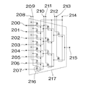
- FIG. 3 is a diagram for explaining the configuration of the multiplexer-type programmable wiring switch of the reconfigurable integrated circuit of the present invention
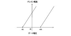
- FIG. 4 is a non-volatile configuration of the programmable wiring switch used in the reconfigurable integrated circuit of the present invention
- FIG. 6 is a diagram for explaining drain current-control gate voltage characteristics of the nonvolatile memory element. This will be described with reference to these drawings.
- the programmable wiring switch 217 has a switch structure in which a plurality of nonvolatile memory elements 216 are arranged so as to constitute a multiplexer type switching circuit.
- a flash memory cell type nonvolatile memory element is used as each nonvolatile memory element 216 constituting the programmable wiring switch.
- This flash memory cell type non-volatile memory element has a floating gate structure, and is accumulated in the floating gate as shown in FIG. 4 by tunneling electrons to or from the floating gate. In this state, a positive threshold voltage + Vt and a negative threshold voltage ⁇ Vt corresponding to the amount of electric charge are obtained, and the conduction state or the non-conduction state is controlled.
- Such characteristics are well known as flash memory cell type nonvolatile memory elements.
- the nonvolatile memory element 216 constituting the multiplexer-type programmable wiring switch 217 here is a nonvolatile memory element in which a positive threshold voltage and a negative threshold voltage can be selectively written by a control terminal. Any type of transistor structure can be used.
- the multiplexer-type programmable wiring switch 217 includes a plurality of signal input terminals 200 to 207, a signal output terminal 215, a plurality of nonvolatile memory elements 216, and a conduction state or a non-conduction state of the plurality of nonvolatile memory elements 216.
- the programmable wiring switch 217 selects one of the voltage signals input to the plurality of signal input terminals 200 to 207 and forms a propagation path of the signal output to one signal output terminal 215 by a switching function.
- the propagation path of the selected signal is set by circuit information stored in the nonvolatile memory element 216 as an element of each switch function.
- a nonvolatile memory element 216 having a switching function is arranged in a multiple-stage binary tree structure in a signal propagation path from the signal input terminal 200-207 to the signal output terminal 215.
- two control terminals 208-209, 210-211, 212-213 are provided, and a control gate of one nonvolatile memory element 216 of each child of each stage is shared by one control terminal. Connecting. The control gates of the remaining nonvolatile memory elements 216 are connected in common to the other control terminal.
- the substrate regions (threshold control terminals) of all the nonvolatile memory elements 216 are connected to the control terminal 214 in common.
- the control terminals 208-213 connected to the control gate of the nonvolatile memory element 216 By inputting an appropriate control signal to the control terminals 208-213 connected to the control gate of the nonvolatile memory element 216, the conduction state or non-conduction state of the nonvolatile memory element arranged in the signal path is set, and the signal input
- the wiring path is set so that any of the input signals from the terminals 200-207 is selectively output to the signal output terminal 215.
- the wiring path is set based on the storage information stored in each nonvolatile storage element 216.
- the erase operation In the erase operation, the signal input terminals 200-207 and the signal output terminal 215 are set in a floating state, and the control terminals 208-213 are set at 0V.
- an erase voltage + Vera which is a positive high voltage
- the control terminal 214 By applying an erase voltage + Vera, which is a positive high voltage, to the control terminal 214, electrons tunnel from the floating gates of all the nonvolatile memory elements 216 to the substrate, and the threshold voltage of all the nonvolatile memory elements 216 is Negative threshold voltage ⁇ Vt. Thereby, the erase operation is completed.
- the write operation is performed after the erase operation is performed.
- the write operation is sequentially performed at each stage of the nonvolatile memory element 216 constituting the binary tree structure. Since each stage is provided with two control terminals, a write operation is performed for each of the plurality of nonvolatile memory elements 216 connected to each control terminal of each stage.
- a threshold voltage is written as a negative voltage ⁇ Vt to a plurality of nonvolatile memory elements 216 connected to one control terminal (208 or 209) at a certain stage, the other control terminal (209 or 208) is written.
- the threshold voltage is written to the plurality of nonvolatile memory elements 216 connected to the positive threshold voltage + Vt. This operation is sequentially performed from the stage near the signal input terminals 200 to 207 in the direction of the output signal terminal 215.
- the signal input terminals 200-207 are floating.
- the control terminal 214 is set to 0V.
- the control terminal (208 or 209) to which the control gates of the selected nonvolatile memory elements 216 to be written in the write selection stage are commonly connected applies a write voltage + Vpgm which is a positive high voltage
- a control terminal (209 or 208) to which the control gates of the non-selected non-volatile memory elements 216 that are not to be written in the selected stage are commonly connected applies 0V.
- a positive voltage + Vpass is applied to the control terminals (210-213) to which the control gates of all the nonvolatile memory elements 216 in the write non-selected stage are connected in common.
- the signal output terminal 215 is set to 0V. Since a positive voltage + Vpass is applied to the control terminals (210-213), 0V applied to the signal output terminal 215 passes through the nonvolatile memory element 216 in the write non-selection stage, and the write selection nonvolatile in the write selection stage. The data is transferred to the storage element 216.
- the threshold voltage of the memory element 216 is a positive voltage + Vt.
- the write inhibit voltage + Viht is applied to the signal output terminal 215.
- the + Viht applied to the signal output terminal 215 is transferred to the write selection nonvolatile memory element 216 in the write selection stage via the nonvolatile memory element 216 in the write non-selection stage. This suppresses the tunneling of electrons from the substrate of the selected nonvolatile memory element 216 that is the write target of the write selection stage to the floating gate, and as a result, the selection that is the write target of the write selection stage is selected. Further, the threshold voltage of the nonvolatile memory element 216 maintains the negative voltage ⁇ Vt.
- the positive voltage + Vpass applied to the control terminals (210-213) connected in common to the control gates of all the nonvolatile memory elements 216 in the write non-selected stage is the write prohibition applied to the signal output terminal 215.
- the voltage + Viht is a voltage value sufficient to transfer the voltage without being attenuated to the selected nonvolatile memory element 216 to be written in the write selection stage, and has a positive threshold voltage + Vt Is a voltage at which the non-volatile memory element 216 having a sufficient conductivity.
- the two control terminals connected to all the nonvolatile memory elements 216 in the read selection stage are set to 0V.
- the control terminal 214 is set to 0V.
- a control terminal to which the control gates of all the nonvolatile memory elements 216 in the read non-selection stage are connected in common applies a positive voltage + Vpass.
- a read voltage + Vread is applied to the signal output terminal 215.
- One of the signal input terminals to which the selected nonvolatile memory element 216 to be read in the read selection stage is electrically connected is set to 0 V, and the other signal input terminals are set to be floating.
- the selected nonvolatile memory element 216 that is the read target of the read selection stage is in the conductive state or the non-conductive state, and the selected nonvolatile memory that is the read target of the read selection stage is determined. Whether or not a desired threshold voltage (+ Vt or ⁇ Vt) is written to the element 216 is confirmed with respect to all the nonvolatile memory elements 216 constituting the programmable wiring switch 217. In the case where there are a plurality of signal input terminals that are electrically connected to the selected nonvolatile memory element 216 to be read in the read selection stage, all of them may be set to 0V, or only one of them may be set to 0V. It is good.
- the programmable wiring switch forms a propagation path for propagating an electrical signal between the routing wirings in the vertical direction and the horizontal direction in accordance with the storage state stored in the nonvolatile memory element constituting the programmable wiring switch.
- the control terminals 208-214 are set to 0V. In this state, a signal is input from the input signal terminals 200-207.
- the programmable wiring switch 217 having a binary tree structure in one stage, one nonvolatile memory element 216 has a positive threshold voltage + Vt, and the other nonvolatile memory element 216 has a negative threshold voltage. Therefore, either one is in a conductive state and the other is in a non-conductive state. As a result, a signal propagation path through which the voltage signal from any one of the signal input terminals 200-207 propagates to the signal output terminal 215 is formed, and the input signal is output to the signal output terminal 215.
- FIG. 5 is a diagram for explaining an application example of the programmable wiring switch 217 to the switch matrix 102 in the reconfigurable integrated circuit of the present invention.
- the switch matrix 102 that provides the function of signal propagation between the routing wiring 326 and the routing wiring 327 is provided with multiplexer-type programmable wiring switches 300-303 as described with reference to FIG. Control signal lines 316 to 323 for controlling the programmable wiring switches 300 to 303 are provided. In relation to this control, switch field effect transistors 304-307, 312-315 and multiplexer circuits 308-310 are provided.
- the control terminals of the programmable wiring switch 300 and the programmable wiring switch 301 are commonly connected to the control signal line 316, and the signal input terminals of the programmable wiring switch 300 and the programmable wiring switch 301 are controlled by the control signal line 322.
- a signal line from the wiring 327 is commonly connected via the switch field effect transistors 312 and 313.
- the control terminals of the programmable wiring switch 302 and the programmable wiring switch 303 are commonly connected to the control signal line 317, and the signal input terminals of the programmable wiring switch 302 and the programmable wiring switch 303 are controlled by the control signal line 323.
- Signal lines from the routing wiring 326 are connected via switch field effect transistors 314 and 315 in common.
- Switch field effect transistors (hereinafter abbreviated as switch FETs) 312 to 315 are connected to signal input terminals of the programmable wiring switches 300 to 303, respectively.
- the gates of the switch FETs 312 and 313 are commonly connected to the control signal line 322, and the gates of the switch FETs 314 and 315 are commonly connected to the control signal line 323.
- Switch FETs 304 and 306 are respectively connected to signal output terminals of the programmable wiring switch 300 and the programmable wiring switch 302, and are connected in common to the control signal line 324 through these.
- Switch FETs 305 and 307 are connected to signal output terminals of the programmable wiring switch 301 and the programmable wiring switch 303, respectively, and are connected in common to the control signal line 325 through these.
- the signal output terminals of the programmable wiring switch 300 and the programmable wiring switch 302 are connected to one of the input terminals of the multiplexer circuits 308 and 310, respectively.
- the signal output terminals of the programmable wiring switch 301 and the programmable wiring switch 303 are connected to one of the input terminals of the multiplexer circuits 309 and 311, respectively.
- One input terminal of the multiplexer circuit 308-311 is grounded to 0V.
- the control terminals of the multiplexer circuits 308 and 309 are commonly connected to the control signal line 320, and the output signal from the programmable wiring switch 300 and the programmable wiring switch 301 or 0 V is selectively applied to the routing wiring 326 according to the signal from the control signal line 320. Output to.
- the multiplexer circuits 310 and 311 are connected in common to the control signal line 321, and an output signal from the programmable wiring switch 302 and the programmable wiring switch 303 or 0 V is selectively applied to the routing wiring 327 by a signal from the control signal line 321. Output.
- control signal lines 316 to 325 are connected to a control circuit similar to the control circuit 104 described with reference to FIG. 2, and an appropriate signal for each programmable wiring switch operation for performing an erase operation, a write operation, and a confirmation read operation. Is propagated to the programmable wiring switch.
- the erase operation will be described.
- 0 V is applied to the control terminals 316 and 317 connected to the control gates of the nonvolatile memory elements constituting the programmable wiring switches 300 to 303.
- the switch FETs 312 to 315 are turned off, and as a result, the signal input terminals of the programmable wiring switches 300 to 303 are set in a floating state.
- 0V is applied to the control signal lines 318 and 319, and a signal for selecting the multiplexer circuit 308-311 to output 0V is applied to the control signal lines 320 and 321.
- the signal output terminals of the programmable wiring switches 300-303 are set in a floating state. In this state, an erase voltage + Vera, which is a positive high voltage, is applied to a control signal line (not shown) connected to the substrate of the nonvolatile memory element that constitutes the programmable wiring switch 300-303. This tunnels electrons from the floating gate of the nonvolatile memory element to the substrate.
- the erase operation may be performed for each programmable wiring switch that commonly connects the control signal lines for the erase operation, or may be performed collectively for the entire chip.
- the programmable wiring switches 300 to 303 are provided for each nonvolatile memory element in each stage because nonvolatile memory elements are arranged in multiple stages so as to constitute a multiplexer-type switch as described with reference to FIG.
- the control signal lines 320 and 321 are applied with a signal for selecting the multiplexer circuit 308-311 to output 0V.
- the routing wirings 326 and 327 are all set to 0V.
- the selected programmable wiring switch to be written is applied to the control signal line to which the selected programmable wiring switch is connected in common, for example, the control signal line 316, respectively, as the write voltage + Vpgm and + Vpass.
- a signal voltage that makes the switch FETs 304 and 305 conductive is applied to the control signal line 318, and 0 V or a write inhibit voltage + Viht is applied to the control signal lines 324 and 325, whereby the programmable wiring switch 300- A write operation is performed on the selected non-volatile storage element 301.
- 0 V is applied to the control signal line to which the non-selected programmable wiring switches 302 to 303 not to be written are commonly connected, for example, the control signal line 317, and the switches FETs 306 and 307 are turned off.
- 0 V is applied to the control signal line 319, 0 V applied to the control signal lines 324 and 325 or the write inhibit voltage + Viht is applied to the signal output terminals of the non-selected programmable wiring switches 302-303 not to be written. Propagation is cut off and erroneous writing of unselected programmable wiring switches 302-303 that are not to be written is prevented.
- the confirmation read operation Similar to the write operation, the read operation is performed for each of the plurality of programmable wiring switches connected in common to each of the control signal line 316 and the control line 317. In the read operation, a signal for selecting the multiplexer circuit 308-311 to output 0 V is applied to the control signal lines 320 and 321. As a result, the routing wirings 326 and 327 are all set to 0V.
- a voltage of + Vpass or 0V is applied to the control signal line commonly connected to the programmable wiring switch selected for confirmation reading, for example, the control signal line 316, and the switch A signal voltage that makes the FETs 304 and 305 conductive is applied to the control signal line 318, and a read voltage + Vread is applied to the control signal lines 324 and 325.
- a control signal line 322 In order to set the signal input terminal of the selected programmable wiring switch to be read corresponding to the nonvolatile memory element selected for reading in the programmable wiring switch selected for confirmation reading to 0V, An appropriate signal is input to the control signal line 322 so that the switch FETs 312 and 313 are sequentially turned on.
- a control signal line such as a control signal line 317, to which unselected programmable wiring switches that are not to be read are commonly connected is applied with 0 V, and a control signal is set so that the switches FETs 306 and 307 become non-conductive. Apply 0 V to line 319.
- control signal lines 324 and 325 have the applied read voltage + Vreadga, the propagation to the signal output terminals of the non-selected programmable wiring switches 302 and 303 not to be read, and the read non-selected programmable wiring switch The erroneous reading of 302 and 303 is prevented.
- the operation of the programmable wiring switch will be described.
- 0 V is applied to the control signal lines 316-319.
- a signal propagation path from one of the plurality of signal input terminals to the signal output terminal according to the positive threshold voltage + Vt and the negative threshold voltage ⁇ Vt written to the nonvolatile memory element in the programmable wiring switch 300-303 Is set, and the switch FET 304-307 is turned off.
- the control signal lines 324 and 325 are set to 0V.
- the control signal lines 322 and 323 apply a voltage that makes the switch FETs 312-315 conductive, and connect the signal input terminals of all the programmable wiring switches to the routing wirings 326 and 327.
- the control signal lines 320 and 321 are inputted with a control signal such that the multiplexer circuit 308-311 selectively outputs an output signal from the programmable wiring switch 300-303.
- the programmable wiring switch in the functional block 101 has the same circuit configuration as the programmable wiring switch in the switch matrix as described above, and thus operates in the same manner as in the switch matrix 102.
- the erase operation, the write operation, the confirmation read operation, and the programmable wiring switch operation can be performed inside the functional block 101.
Landscapes
- Physics & Mathematics (AREA)
- Mathematical Physics (AREA)
- Engineering & Computer Science (AREA)
- Computer Hardware Design (AREA)
- Computing Systems (AREA)
- General Engineering & Computer Science (AREA)
- Computer Networks & Wireless Communication (AREA)
- Logic Circuits (AREA)
- Design And Manufacture Of Integrated Circuits (AREA)
Abstract
基本の回路要素の基本タイルの間の配線状態を設定する複数のプログラマブル配線スイッチが不揮発性記憶素子で構成される再構成可能集積回路を提供する。再構成可能集積回路は、複数の入力端子と出力端子を備えるマルチプレクサ型のプログラマブル配線スイッチを構成する複数の不揮発性記憶素子を備える。入力端子から出力端子への信号電圧の伝搬経路にスイッチ機能を有する電界効果トランジスタ構造の不揮発性記憶素子が配置されており、不揮発性記憶素子が入力端子からの信号電圧を選択的に出力端子に伝搬するマルチプレクサ型のプログラマブル配線スイッチを構成するため、不揮発性記憶素子に対して導通状態もしくは非導通状態とする結線情報を記憶する書き込み動作、結線情報を消去する消去動作と、不揮発性記憶素子の導通状態もしくは非導通状態を確認する読み出し動作を直接行う制御回路を備える。
Description
本発明は、半導体集積回路により構成される再構成可能集積回路に関し、特に、基本の回路要素の基本タイルの間の配線状態を設定する複数のプログラマブル配線スイッチが不揮発性記憶素子で構成される再構成可能集積回路に関する。
自在に回路構成を変更できるFPGA(Filed Programmable Gate Array)に代表される再構成可能集積回路は、デバイスに内蔵された記憶素子に回路構成情報を記憶することによって、ルーティング配線の結線状態やロジックブロックにおける論理機能、ルーティング配線とロジックブロックの相互接続状態を自由かつ柔軟に変更することが可能なデバイスである。ユーザは、デバイス内部の記憶素子に外部から回路構成情報を書き込むことによって、所望の規模、所望の機能を有する論理回路を構成することができる。
再構成可能集積回路における柔軟な再構成機能を実現するため、再構成可能集積回路においては、複数の基本理回路ブロックおよび当該基本回路ブロックの間の結線状態を制御する複数の配線スイッチブロックに複数のプログラマブル配線スイッチが実装される。
プログラマブル配線スイッチは、スイッチ機能の電界効果トランジスタ(スイッチFET)と、スイッチFETの導通状態もしくは非導通状態を記憶するための記憶素子から構成されている。
ルーティング配線同士もしくはルーティング配線とロジックブロックとの配線を、プログラマブル配線スイッチを介して接続することによって、ルーティング配線同士もしくはルーティング配線とロジックブロックの接続もしくは非接続を、プログラマブル配線スイッチに内蔵される記憶素子の記憶状態で決定することができる。
プログラマブル配線スイッチは、複数の入力端子と1つの出力端子を有し、この複数の入力への信号電圧を選択的に出力することが可能なマルチプレクサ回路を構成する複数のスイッチFETと、このマルチプレクサ回路を構成するスイッチFETの導通状態もしくは非導通状態を記憶するための複数の記憶素子とを有する。この記憶素子としてはSRAM(Static Random Acces Memory)が用いられる。
このようなプログラマブル配線スイッチについては、FPGAのコンフィギャレーション情報の盗聴防止や、プログラマブル配線スイッチ、特に記憶素子の消費電力低減を目的として、特許文献1,2,3,4,5,6に示されるように、情報記憶素子としては、不揮発性記憶素子を用いたプログラマブル配線スイッチが提案されている。
例えば、特許文献1または特許文献2に記載の不揮発性記憶素子が設けられているプログラマブル配線スイッチでは、スイッチFETと、電子をトンネリングする機能かつフローティングゲート蓄積電荷量を確認する機能を有する素子が、フローティングゲートを共有し、2つのFETが一つの基本素子を構成しているものが用いられる。
また、特許文献3,特許文献4,特許文献5,または特許文献6に記載の不揮発性記憶素子が設けられているプログラマブル配線スイッチでは、スイッチFETと、電子をトンネリングする機能を有する素子と、フローティングゲート蓄積電荷量を確認する機能を有する素子が、フローティングゲートを共有し、3つのFETが一つの基本素子を構成しているものが用いられる。
特許文献1または特許文献2に記載の不揮発性記憶素子が設けられているプログラマブル配線スイッチにおいては、2つのFETが一つの基本素子を構成しているので、スイッチ面積が増加するという問題点がある。
また、特許文献3,特許文献4,特許文献5,または特許文献6に記載の不揮発性記憶素子が設けられているプログラマブル配線スイッチにおいては、3つのFETが一つの基本素子を構成しているので、スイッチ面積が増加するという問題点がある。
さらに、特許文献1,特許文献2,特許文献3,特許文献4,特許文献5,特許文献6に記載されている不揮発性記憶素子を有するプログラマブル配線スイッチは、マルチプレクサ型のプログラマブル配線スイッチに対応していないという問題点がある。マルチプレクサ型のプログラマブル配線スイッチは、FPGAで現在主流となっている。
本発明は、上記のような問題を解決するためになされたものであり、本発明の目的は、基本の回路要素の基本タイルの間の配線状態を設定する複数のプログラマブル配線スイッチが不揮発性記憶素子で構成される再構成可能集積回路を提供することにある。
上記のような目的を達成するため、本発明による再構成可能集積回路は、基本的な構成として、複数の入力端子と出力端子を備えるマルチプレクサ型のプログラマブル配線スイッチを構成する複数の不揮発性記憶素子を備えた再構成可能集積回路であって、前記入力端子から前記出力端子への信号電圧の伝搬経路にスイッチ機能を有する電界効果トランジスタ構造の不揮発性記憶素子が配置されており、前記不揮発性記憶素子が前記入力端子からの信号電圧を選択的に出力端子に伝搬するマルチプレクサ型のプログラマブル配線スイッチを構成し、前記不揮発性記憶素子に対して導通状態もしくは非導通状態とする結線情報を記憶するための制御信号線を備える。
本発明の再構成可能集積回路においては、マルチプレクサ型のプログラマブル配線スイッチを構成する複数段の不揮発性記憶素子に対して、導通状態もしくは非導通状態とする結線情報を記憶する書き込み動作、結線情報を消去する消去動作と、不揮発性記憶素子の導通状態もしくは非導通状態を確認する読み出し動作を直接行う制御回路を備える。
また、本発明による再構成可能集積回路は、一つの態様として、基本の回路要素である基本タイルの複数個がアレイ状に配置された構造であり、前記基本タイルの間を結線するルーティング配線、前記ルーティング配線の間を結線するスイッチマトリックス、前記スイッチマトリックスに接続された機能ブロックから前記基本タイルが構成されている再構成可能集積回路において、前記スイッチマトリックスにスイッチ機能を有する複数段の電界効果トランジスタ構造の不揮発性記憶素子から構成されるマルチプレクサ型のプログラマブル配線スイッチを備え、前記マルチプレクサ型のプログラマブル配線スイッチを構成する各段の不揮発性記憶素子に対して導通状態もしくは非導通状態とする結線情報を記憶する書き込み動作、前記結線情報を読み出す確認読み出し動作、および前記結線情報を消去する消去動作のための制御信号線および制御回路を備える。
また、本発明による再構成可能集積回路は、別の態様として、基本の回路要素である基本タイルの複数個がアレイ状に配置された構造であり、前記基本タイルの間を結線するルーティング配線、前記ルーティング配線の間を結線するスイッチマトリックス、前記スイッチマトリックスに接続された機能ブロックから前記基本タイルが構成されている再構成可能集積回路において、前記機能ブロックにスイッチ機能を有する複数段の電界効果トランジスタ構造の不揮発性記憶素子から構成されるマルチプレクサ型のプログラマブル配線スイッチを備え、前記マルチプレクサ型のプログラマブル配線スイッチを構成する不揮発性記憶素子に対して導通状態もしくは非導通状態とする結線情報を記憶する書き込み動作、前記結線情報を読み出す確認読み出し動作、および前記結線情報を消去する消去動作のための制御信号線および制御回路を備える。
この場合に、本発明の再構成可能集積回路において、消去動作を行う場合には、プログラマブル配線スイッチを構成するすべての不揮発性記憶素子を選択し、不揮発性記憶素子に対して一括して消去動作を行う。
従来の不揮発性記憶素子を備えたプログラマブル配線スイッチが、スイッチFET、確認読みし用FETと、書き込み動作、消去動作用デバイスの3種類、もしくは、スイッチFETと書き込み動作、消去動作かつ確認読み出し用FETの2種類のFETが必要であったのに対して、本発明によるプログラマブル配線スイッチでは、スイッチFET、書き込み動作、消去動作、確認読み出し動作のすべての機能を一つの電界効果トランジスタ構造の不揮発性記憶素子で行うことができるので、プログラマブル配線スイッチの面積を小さくすることができる。
本発明によるマルチプレクサ型のプログラマブル配線スイッチを構成する不揮発性記憶素子を備えた再構成可能集積回路は、プログラマブル配線スイッチを構成する不揮発性記憶素子に対して直接的に消去動作、書き込み動作、確認読み出し動作を行うことが可能であり、それと同時に、不揮発性記憶素子は、プログラマブル配線スイッチとしての機能を有しているので、従来の不揮発性記憶装置を有する再構成可能集積回路と比べて専有面積を小さくすることができる。
以下、本発明を実施する一形態について、図面を参照して説明する。図1は、本発明による再構成可能集積回路を構成する基本の回路要素である基本タイルの構造を説明する図である。基本タイル100は、機能ブロック101、スイッチマトリックス102、ルーティング配線103、およびプログラマブル配線スイッチを構成する不揮発性記憶素子のための制御信号線105から構成される。機能ブロック101は、論理機能を外部から書き換え可能なロジックブロックを用いたロジックブロックまたはI/Oブロックとして構成される。プログラマブル配線スイッチを構成する不揮発性記憶素子はスイッチマトリックス102に内蔵されるが、機能ブロック101の一部にプログラマブル配線スイッチが内蔵されるような構成とされても良い。
スイッチマトリックス102には、複数のプログラマブル配線スイッチが内蔵される。機能ブロック101とスイッチマトリックス102とは、図示されていないが配線で相互に接続されている。スイッチマトリックス102の内部のプログラマブル配線スイッチの導通状態もしくは非導通状態により、電圧信号をルーティング配線103の間で伝搬させたり、ルーティング配線103から機能ブロック101へ伝搬させたり、機能ブロック101で処理した電圧信号をルーティング配線103へ伝搬させたりする。
スイッチマトリックス102および機能ブロック101に内蔵されているプログラマブル配線スイッチを構成する複数の不揮発性記憶素子は、この不揮発性記憶素子の導通状態もしくは非導通状態を設定するため、制御信号線105によって書き込み、消去、確認読み出し動作が行われる。
図2は、本発明による再構成可能集積回路の全体の構成を説明する図である。本発明の再構成可能集積回路は、基本タイル100をアレイ状に配置した構造である。不揮発性記憶素子を制御するための制御信号線105は、制御回路104に接続される。
制御回路104は、プログラマブル配線スイッチを構成する不揮発性記憶素子の導通状態もしくは非導通状態を設定するための書き込み回路、消去回路、確認読み出し回路を備えている。制御回路104は、典型的には、従来から公知の不揮発性記憶装置を構成する不揮発性記憶素子に対する書き込みおよび読み出しを制御する制御回路を用いる。このような制御回路の構成は公知であり、ここでの詳細な説明は省略する。
制御回路104は、再構成可能集積回路の全体の不揮発性記憶素子を制御するように構成される。または、所定の数の基本タイルの区画に対して、複数の不揮発性記憶素子の集合を形成し、その複数の不揮発性記憶素子の集合に対して、その不揮発性記憶素子の集合のそれぞれに対して制御回路を設け、それぞれの集合を個別に制御するように構成されても良い。
図3は、本発明の再構成可能集積回路のマルチプレクサ型のプログラマブル配線スイッチの構成を説明する図であり、図4は、本発明の再構成可能集積回路で用いられるプログラマブル配線スイッチを構成する不揮発性記憶素子のドレイン電流-制御ゲート電圧特性を説明する図である。これらの図を参照して説明する。
図3に示すように、プログラマブル配線スイッチ217は、複数の不揮発性記憶素子216がマルチプレクサ型のスイッチング回路を構成するように配置されたスイッチ構造となっている。プログラマブル配線スイッチを構成する個々の不揮発性記憶素子216としては、フラッシュメモリセルタイプの不揮発性記憶素子を用いる。このフラッシュメモリセルタイプの不揮発性記憶素子は、フローティングゲート構造を有しており、フローティングゲートに対して、もしくはフローティングゲートから電子をトンネリングすることにより、図4に示すように、フローティングゲートに蓄積された電荷量に対応した正のしきい値電圧+Vtと負のしきい値電圧-Vtの状態となって、導通状態もしくは非導通状態が制御されるものである。このような特性については、フラッシュメモリセルタイプの不揮発性記憶素子として周知である。
ここでのマルチプレクサ型のプログラマブル配線スイッチ217を構成する不揮発性記憶素子216は、正のしきい値電圧と負のしきい値電圧を、制御端子によって選択的に書き込み可能である不揮発性記憶素子であれば、いずれのタイプのトランジスタ構造でも利用できる。
マルチプレクサ型のプログラマブル配線スイッチ217は、複数の信号入力端子200-207と、1つの信号出力端子215と、複数の不揮発性記憶素子216と、複数の不揮発性記憶素子216の導通状態または非導通状態を制御するための制御信号を入力する制御端子208-214とを有しており、複数の不揮発性記憶素子216が入力端子から出力端子の方向に多段に接続された構造となっているスイッチである。
プログラマブル配線スイッチ217では、複数の信号入力端子200-207に入力される電圧信号の1つが選択されて1つの信号出力端子215に出力される信号の伝搬経路をスイッチング機能により形成する。この選択される信号の伝搬経路は、各スイッチ機能の要素の不揮発性記憶素子216に記憶される回路情報により設定される。
プログラマブル配線スイッチ217においては、信号入力端子200-207から信号出力端子215への信号の伝搬経路にスイッチ機能の不揮発性記憶素子216を複数段の二分木構造で配置する。各段において、二つの制御端子(208-209,210-211,212-213)を設け、一つの制御端子に、各段のそれぞれの子の一方の不揮発性記憶素子216の制御ゲートを共通に接続する。残りの不揮発性記憶素子216の制御ゲートを共通としてもう一方の制御端子に接続する。
また、すべての不揮発性記憶素子216の基板領域(しきい値制御端子)は制御端子214に共通に接続される。不揮発性記憶素子216の制御ゲートに接続される制御端子208-213に適切な制御信号を入力することにより、信号経路に配置した不揮発性記憶素子の導通状態もしくは非導通状態が設定され、信号入力端子200-207からのいずれかの入力信号が、選択的に信号出力端子215へ出力されるように配線経路が設定される。この配線経路の設定は、各不揮発性記憶素子216に記憶された記憶情報により設定される。
次に、具体的な不揮発性記憶素子216に配線経路を設定する記憶情報を記憶する動作について、消去動作、書き込み動作、確認読み出し動作、プログラマブル配線動作の順に説明する。まず、消去動作を行い、消去動作を行ってから書き込み動作を行い、書き込まれた内容は確認読み出し動作により読み出しする。
消去動作について説明する。消去動作では、信号入力端子200-207と信号出力端子215をフローティングとし、制御端子208-213は0Vとする。制御端子214に正の高電圧である消去電圧+Veraを印加することよって、すべての不揮発性記憶素子216のフローティングゲートから基板へ電子がトンネルし、すべての不揮発性記憶素子216のしきい値電圧は負のしきい値電圧-Vtとなる。これにより、消去動作が完了する。
次に、書き込み動作について説明する。書き込み動作は、消去動作が行われた後に行われる。書き込み動作は、二分木構造を構成している不揮発性記憶素子216の各段で順次に行われる。各段はそれぞれ二つの制御端子を設けているので、各段の各制御端子に接続されている複数の不揮発性記憶素子216ごとに書き込み動作を行う。ある段において、一方の制御端子(208または209)に接続される複数の不揮発性記憶素子216に、しきい値電圧を負の電圧-Vtとして書き込んだ場合、もう一方の制御端子(209または208)に接続する複数の不揮発性記憶素子216には、しきい値電圧を正のしきい値電圧+Vtとなるように書き込む。この動作を、信号入力端子200-207に近い側の段から出力信号端子215の方向へ順番に行う。
具体的に説明する。信号入力端子200-207はフローティングとする。制御端子214は0Vとする。書き込み選択段の書き込み対象となっている選択された不揮発性記憶素子216の制御ゲートが共通して接続する制御端子(208または209)は、正の高電圧である書き込み電圧+Vpgmを印加し、書き込み選択段の書き込み対象となっていない非選択の不揮発性記憶素子216の制御ゲートが共通して接続する制御端子(209または208)は0Vを印加する。書き込み非選択段のすべての不揮発性記憶素子216の制御ゲートが共通して接続する制御端子(210-213)については正の電圧+Vpassを印加する。
書き込み選択段の書き込み対象となっている選択された不揮発性記憶素子216に正のしきい値電圧+Vtを書き込む場合、信号出力端子215を0Vとする。制御端子(210-213)は正の電圧+Vpassを印加しているので、信号出力端子215に印加した0Vが書き込み非選択段の不揮発性記憶素子216を経由して書き込み選択段の書き込み選択不揮発性記憶素子216まで転送される。これにより、書き込み選択段の書き込み対象となっている選択された不揮発性記憶素子216の基板からフローティングゲートへ電子がトンネルし、その結果、書き込み選択段の書き込み対象となっている選択された不揮発性記憶素子216のしきい値電圧は正の電圧+Vtとなる。
書き込み選択段の書き込み対象となっている選択された不揮発性記憶素子216に負のしきい値電圧-Vtを書き込む場合には、信号出力端子215を書き込み禁止電圧+Vihtを印加する。この信号出力端子215に印加した+Vihtは、書き込み非選択段の不揮発性記憶素子216を経由して書き込み選択段の書き込み選択不揮発性記憶素子216まで転送される。これにより、書き込み選択段の書き込み対象となっている選択された不揮発性記憶素子216の基板からフローティングゲートへの電子のトンネルを抑制し、その結果、書き込み選択段の書き込み対象となっている選択された不揮発性記憶素子216のしきい値電圧は負の電圧-Vtを維持する。
この場合において、書き込み非選択段のすべての不揮発性記憶素子216の制御ゲートに共通して接続する制御端子(210-213)に印加する正の電圧+Vpassは、信号出力端子215に印加する書き込み禁止電圧+Vihtを、書き込み選択段の書き込み対象となっている選択された不揮発性記憶素子216に対して、電圧が減衰することなく転送できるだけの十分な電圧値であり、かつ正のしきい値電圧+Vtを有する不揮発性記憶素子216が十分に導通状態となる電圧である。
次に、確認読み出し動作について説明する。確認読み出し動作の場合には、読み出し選択段のすべての不揮発性記憶素子216に接続されている二つの制御端子を0Vとする。制御端子214は0Vとする。読み出し非選択段のすべての不揮発性記憶素子216の制御ゲートが共通して接続する制御端子は正の電圧+Vpassを印加する。信号出力端子215には読み出し電圧+Vreadを印加する。読み出し選択段の読み出し対象となっている選択された不揮発性記憶素子216が電気的に導通している信号入力端子の一つを0Vとし、それ以外の信号入力端子をフローティングとする。
この状態で、読み出し選択段の読み出し対象となっている選択された不揮発性記憶素子216の導通状態、もしくは非導通状態を判断し、読み出し選択段の読み出し対象となっている選択された不揮発性記憶素子216に所望のしきい値電圧(+Vtまたは-Vt)が書き込まれたかどうかを、プログラマブル配線スイッチ217を構成するすべての不揮発性記憶素子216に対して確認する。読み出し選択段の読み出し対象となっている選択された不揮発性記憶素子216に電気的に導通する信号入力端子が複数ある場合は、そのすべてを0Vとしてもよいし、そのいずれか一つだけを0Vとしてもよい。
次に、プログラマブル配線スイッチの動作について説明する。プログラマブル配線スイッチは、当該プログラマブル配線スイッチを構成している不揮発性記憶素子に記憶されている記憶状態にしたがって縦方向および横方向のルーティング配線の間で、電気信号を伝搬させる伝搬経路を形成する。動作において、まず、制御端子208-214を0Vとする。この状態で、入力信号端子200-207から信号を入力する。二分木構造のプログラマブル配線スイッチ217において、ある段においては一方の不揮発性記憶素子216は正のしきい値電圧+Vtを有し、もう一方の不揮発性記憶素子216は負のしきい値電圧を有するので、どちらか一方が導通状態であり、もう一方は非導通状態となっている。これによって、信号入力端子200-207のいずれか一つからの電圧信号が信号出力端子215へ伝搬する信号の伝搬経路が形成され、入力信号が信号出力端子215へ出力される。
図5は、本発明の再構成可能集積回路におけるプログラマブル配線スイッチ217のスイッチマトリックス102への適用例を説明する図である。
図5を参照すると、ルーティング配線326とルーティング配線327と間で信号伝搬の機能を提供するスイッチマトリックス102は、図3により説明したようなマルチプレクサ型のプログラマブル配線スイッチ300-303が設けられ、これらのプログラマブル配線スイッチ300-303を制御するための制御信号線316-323が設けられている。この制御に関係して、スイッチ電界効果トランジスタ304-307,312-315、マルチプレクサ回路308-310が設けられている。
プログラマブル配線スイッチ300およびプログラマブル配線スイッチ301の制御端子は、制御信号線316に共通に接続されると共に、プログラマブル配線スイッチ300およびプログラマブル配線スイッチ301の信号入力端子は、制御信号線322により制御されるルーティング配線327からの信号線が共通にスイッチ電界効果トランジスタ312,313を介して接続されている。
また、プログラマブル配線スイッチ302およびプログラマブル配線スイッチ303の制御端子は、制御信号線317に共通に接続されると共に、プログラマブル配線スイッチ302およびプログラマブル配線スイッチ303の信号入力端子は、制御信号線323により制御されるルーティング配線326からの信号線が共通にスイッチ電界効果トランジスタ314,315を介して接続されている。
プログラマブル配線スイッチ300-303の信号入力端子にはそれぞれスイッチ電界効果トランジスタ(以下、スイッチFETと略称する)312-315が接続される。スイッチFET312と313のそれぞれのゲートは制御信号線322に共通に接続され、スイッチFET314と315のそれぞれのゲートは制御信号線323に共通に接続される。
プログラマブル配線スイッチ300およびプログラマブル配線スイッチ302の信号出力端子にはスイッチFET304と306がそれぞれ接続され、これらを介して制御信号線324に共通に接続される。プログラマブル配線スイッチ301およびプログラマブル配線スイッチ303の信号出力端子にはスイッチFET305と307がそれぞれ接続され、これらを介して制御信号線325に共通に接続される。
プログラマブル配線スイッチ300およびプログラマブル配線スイッチ302の信号出力端子は、マルチプレクサ回路308と310の入力端子の一方に、それぞれ接続される。プログラマブル配線スイッチ301およびプログラマブル配線スイッチ303の信号出力端子は、マルチプレクサ回路309と311の入力端子の一方に、それぞれ接続される。マルチプレクサ回路308-311の一方の入力端子は0Vに接地される。マルチプレクサ回路308と309の制御端子は制御信号線320に共通に接続され、制御信号線320からの信号によって、ルーティング配線326にプログラマブル配線スイッチ300およびプログラマブル配線スイッチ301からの出力信号か0Vを選択的に出力する。
また、マルチプレクサ回路310と311は制御信号線321に共通に接続され、制御信号線321からの信号によって、ルーティング配線327にプログラマブル配線スイッチ302およびプログラマブル配線スイッチ303からの出力信号か0Vを選択的に出力する。
制御信号線316-325は、図2において説明した制御回路104と同様な制御回路に接続されており、消去動作、書き込み動作、確認読み出し動作を行うために、プログラマブル配線スイッチ動作ごとに適切な信号をプログラマブル配線スイッチに伝搬する。
次に、消去動作、書き込み動作、確認読み出し動作、プログラマブル配線スイッチ動作について説明する。
まず、消去動作について説明する。消去動作において、プログラマブル配線スイッチ300-303を構成する不揮発性記憶素子の制御ゲートに接続される制御端子316と317には0Vを印加する。制御端子322と323を0Vとすることにより、スイッチFET312-315を非導通状態とし、その結果、プログラマブル配線スイッチ300-303の信号入力端子をフローティングとする。
制御信号線318と319には0Vを印加し、制御信号線320と321には、マルチプレクサ回路308-311が0Vを出力するように選択する信号を印加する。これにより、プログラマブル配線スイッチ300-303の信号出力端子をフローティングとする。この状態でプログラマブル配線スイッチ300-303を構成する不揮発性記憶素子の基板に接続されている制御信号線(図示せず)に正の高電圧である消去電圧+Veraを印加する。これにより、不揮発性記憶素子のフローティングゲートから基板へ電子をトンネルする。
消去動作は、消去動作用制御信号線を共通に接続するプログラマブル配線スイッチごとに行ってもよいし、チップ全体で一括して行ってもよい。
次に書き込み動作について説明する。書き込みは、制御信号線316または317に共通に接続されている複数のプログラマブル配線スイッチ300-303ごとに行う。プログラマブル配線スイッチ300-303は、図3により説明したようなマルチプレクサ型のスイッチを構成するように不揮発性記憶素子が多段に配置されているので、各段の不揮発性記憶素子ごとに行う。
書き込み動作では、制御信号線322と323に0Vを印加し、スイッチFET312-315を非導通状態とすることにより、プログラマブル配線スイッチ300-303の信号入力端子をフローティングとする。
制御信号線320と321には、マルチプレクサ回路308-311が0Vを出力するように選択する信号を印加する。これによって、ルーティング配線326と327はすべて0Vとなる。書き込み対象となっている選択されたプログラマブル配線スイッチが、共通に接続される制御信号線、例えば制御信号線316には、図3で説明したように、それぞれに書き込み電圧+Vpgmおよび+Vpassの電圧を印加すると共に、スイッチFET304と305を導通状態とするような信号電圧を制御信号線318に印加し、制御信号線324と325には0Vまたは書き込み禁止電圧+Vihtを印加することにより、プログラマブル配線スイッチ300-301の選択された不揮発性記憶素子に書き込み動作を行う。
書き込み対象となっていない非選択のプログラマブル配線スイッチ302-303が共通に接続される制御信号線、例えば制御信号線317には0Vを印加すると共に、スイッチFET306と307が非導通状態となるように制御信号線319に0Vを印加することにより、制御信号線324と325に印加した0Vもしくは書き込み禁止電圧+Vihtが、書き込み対象となっていない非選択のプログラマブル配線スイッチ302-303の信号出力端子への伝搬を遮断し、書き込み対象となっていない非選択のプログラマブル配線スイッチ302-303の誤書き込みを防止する。
次に、確認読み出し動作について説明する。読み出し動作においては、書き込み動作と同様に、制御信号線316および制御線317のそれぞれで共通に接続されている複数のプログラマブル配線スイッチごとに行う。読み出し動作において、制御信号線320と321には、マルチプレクサ回路308-311が0Vを出力するように選択する信号を印加する。これによって、ルーティング配線326と327はすべて0Vとなる。
確認読み出しのために選択されたプログラマブル配線スイッチに共通に接続される制御信号線、例えば、制御信号線316には、図3で説明したように、電圧+Vpassまたは0Vの電圧を印加すると共に、スイッチFET304と305を導通状態とするような信号電圧を制御信号線318に印加し、制御信号線324と325に読み出し電圧+Vreadを印加する。
確認読み出しのために選択されたプログラマブル配線スイッチ内の、読み出しのために選択された不揮発性記憶素子に対応した読み出し対象となっている選択されたプログラマブル配線スイッチの信号入力端子を0Vにするため、スイッチFET312や313を順次導通状態となるように制御信号線322に適切な信号を入力する。読み出し対象となっていない非選択のプログラマブル配線スイッチが共通に接続される制御信号線、例えば、制御信号線317には0Vを印加すると共に、スイッチFET306と307が非導通状態となるように制御信号線319に0Vを印加する。これにより、制御信号線324と325には、印加した読み出し電圧+Vreadga,読み出し対象となっていない非選択のプログラマブル配線スイッチ302と303の信号出力端子への伝搬を遮断し、読み出し非選択プログラマブル配線スイッチ302と303の誤読み出しを防止する。
次に、プログラマブル配線スイッチの動作について説明する。プログラマブル配線スイッチを動作状態とするには、制御信号線316-319は0Vを印加する。プログラマブル配線スイッチ300-303内の不揮発性記憶素子に書き込んだ正のしきい値電圧+Vtと負のしきい値電圧-Vtに従って、複数の信号入力端子の一つから信号出力端子への信号伝搬経路が設定されるとともに、スイッチFET304-307を非導通状態とする。制御信号線324と325は0Vとする。
制御信号線322と323は、スイッチFET312-315が導通状態となるような電圧を印加し、すべてのプログラマブル配線スイッチの信号入力端子をルーティング配線326と327に接続する。制御信号線320と321には、マルチプレクサ回路308-311が選択的に、プログラマブル配線スイッチ300-303からの出力信号を出力するような制御信号を入力する。
本発明の再構成可能集積回路において、機能ブロック101の内部のプログラマブル配線スイッチは、上述したようなスイッチマトリックスにおけるプログラマブル配線スイッチと同様の回路構成であるので、スイッチマトリックス102の場合と同様に動作させることにより、消去動作、書き込み動作、確認読み出し動作、プログラマブル配線スイッチ動作を機能ブロック101内部でも行うことができる。
100 再構成可能集積回路の基本構造
101 機能ブロック
102 スイッチマトリックス
103 ルーティング配線
104 制御回路
105 制御信号線
200-207 信号入力端子
208-214 制御信号線
215 信号出力端子
216 不揮発性記憶素子
217 プログラマブル配線スイッチ
300-303 プログラマブル配線スイッチ
304-307 スイッチFET
308-311 マルチプレクサ回路
312-315 スイッチFET
316-325 制御信号線
326、327 ルーティング配線
101 機能ブロック
102 スイッチマトリックス
103 ルーティング配線
104 制御回路
105 制御信号線
200-207 信号入力端子
208-214 制御信号線
215 信号出力端子
216 不揮発性記憶素子
217 プログラマブル配線スイッチ
300-303 プログラマブル配線スイッチ
304-307 スイッチFET
308-311 マルチプレクサ回路
312-315 スイッチFET
316-325 制御信号線
326、327 ルーティング配線
Claims (5)
- 複数の入力端子と出力端子を備えるマルチプレクサ型のプログラマブル配線スイッチを構成する複数の不揮発性記憶素子を備えた再構成可能集積回路であって、
前記入力端子から前記出力端子への信号電圧の伝搬経路にスイッチ機能を有する電界効果トランジスタ構造の不揮発性記憶素子が配置されて、前記不揮発性記憶素子が前記入力端子からの信号電圧を選択的に出力端子に伝搬するマルチプレクサ型のプログラマブル配線スイッチを構成し、前記不揮発性記憶素子に対して導通状態もしくは非導通状態とする結線情報を記憶するための制御信号線を備える
ことを特徴とする再構成可能集積回路。 - 請求項1に記載の再構成可能集積回路において、
マルチプレクサ型のプログラマブル配線スイッチを構成する複数段の不揮発性記憶素子に対して、導通状態もしくは非導通状態とする結線情報を記憶する書き込み動作、結線情報を消去する消去動作と、不揮発性記憶素子の導通状態もしくは非導通状態を確認する読み出し動作を直接行う制御回路を備える
ことを特徴とする再構成可能集積回路。 - 基本の回路要素である基本タイルの複数個がアレイ状に配置された構造であり、前記基本タイルの間を結線するルーティング配線、前記ルーティング配線の間を結線するスイッチマトリックス、前記スイッチマトリックスに接続された機能ブロックから前記基本タイルが構成されている再構成可能集積回路において、
前記スイッチマトリックスにスイッチ機能を有する複数段の電界効果トランジスタ構造の不揮発性記憶素子から構成されるマルチプレクサ型のプログラマブル配線スイッチを備え、
前記マルチプレクサ型のプログラマブル配線スイッチを構成する各段の不揮発性記憶素子に対して導通状態もしくは非導通状態とする結線情報を記憶する書き込み動作、前記結線情報を読み出す確認読み出し動作、および前記結線情報を消去する消去動作のための制御信号線および制御回路を備える
ことを特徴とする再構成可能集積回路。 - 基本の回路要素である基本タイルの複数個がアレイ状に配置された構造であり、前記基本タイルの間を結線するルーティング配線、前記ルーティング配線の間を結線するスイッチマトリックス、前記スイッチマトリックスに接続された機能ブロックから前記基本タイルが構成されている再構成可能集積回路において、
前記機能ブロックにスイッチ機能を有する複数段の電界効果トランジスタ構造の不揮発性記憶素子から構成されるマルチプレクサ型のプログラマブル配線スイッチを備え、
前記マルチプレクサ型のプログラマブル配線スイッチを構成する不揮発性記憶素子に対して導通状態もしくは非導通状態とする結線情報を記憶する書き込み動作、前記結線情報を読み出す確認読み出し動作、および前記結線情報を消去する消去動作のための制御信号線および制御回路を備える
ことを特徴とする再構成可能集積回路。 - 請求項2乃至4に記載の再構成可能集積回路において、
消去動作を行う場合には、プログラマブル配線スイッチを構成するすべての不揮発性記憶素子を選択し、不揮発性記憶素子に対して一括して消去動作を行う
ことを特徴とする再構成可能集積回路。
Priority Applications (1)
| Application Number | Priority Date | Filing Date | Title |
|---|---|---|---|
| US13/126,506 US8461870B2 (en) | 2008-10-30 | 2009-10-26 | Non-volatile multiplexer-type programmable routing switch |
Applications Claiming Priority (2)
| Application Number | Priority Date | Filing Date | Title |
|---|---|---|---|
| JP2008279573A JP4512752B2 (ja) | 2008-10-30 | 2008-10-30 | 再構成可能集積回路 |
| JP2008-279573 | 2008-10-30 |
Publications (1)
| Publication Number | Publication Date |
|---|---|
| WO2010050440A1 true WO2010050440A1 (ja) | 2010-05-06 |
Family
ID=42128802
Family Applications (1)
| Application Number | Title | Priority Date | Filing Date |
|---|---|---|---|
| PCT/JP2009/068347 Ceased WO2010050440A1 (ja) | 2008-10-30 | 2009-10-26 | 再構成可能集積回路 |
Country Status (3)
| Country | Link |
|---|---|
| US (1) | US8461870B2 (ja) |
| JP (1) | JP4512752B2 (ja) |
| WO (1) | WO2010050440A1 (ja) |
Cited By (1)
| Publication number | Priority date | Publication date | Assignee | Title |
|---|---|---|---|---|
| CN111279417A (zh) * | 2017-10-06 | 2020-06-12 | 阿姆有限公司 | 可重配置电路体系架构 |
Families Citing this family (3)
| Publication number | Priority date | Publication date | Assignee | Title |
|---|---|---|---|---|
| US9106231B2 (en) | 2012-01-11 | 2015-08-11 | Nec Corporation | Bidirectional buffer and control method thereof |
| KR101906966B1 (ko) * | 2012-11-05 | 2018-12-07 | 삼성전자주식회사 | 논리 장치 및 이의 동작 방법 |
| JP2016178183A (ja) | 2015-03-19 | 2016-10-06 | 株式会社東芝 | 半導体集積回路 |
Citations (3)
| Publication number | Priority date | Publication date | Assignee | Title |
|---|---|---|---|---|
| JP2000323671A (ja) * | 1998-11-06 | 2000-11-24 | Rohm Co Ltd | 信号保持回路、半導体装置、ゲートアレイおよびicカード |
| JP2003115754A (ja) * | 2001-06-06 | 2003-04-18 | Matsushita Electric Ind Co Ltd | 不揮発性セレクタ及び集積回路装置 |
| WO2004059838A1 (ja) * | 2002-12-25 | 2004-07-15 | Matsushita Electric Industrial Co., Ltd. | 不揮発性ラッチ回路及びその駆動方法 |
Family Cites Families (14)
| Publication number | Priority date | Publication date | Assignee | Title |
|---|---|---|---|---|
| WO1996001499A1 (en) | 1994-07-05 | 1996-01-18 | Zycad Corporation | A general purpose, non-volatile reprogrammable switch |
| US5633518A (en) | 1995-07-28 | 1997-05-27 | Zycad Corporation | Nonvolatile reprogrammable interconnect cell with FN tunneling and programming method thereof |
| US5894148A (en) | 1996-08-09 | 1999-04-13 | Gatefield Corporation | Floating gate FPGA cell with counter-doped select device |
| US6252273B1 (en) | 1996-08-09 | 2001-06-26 | Actel Corporation | Nonvolatile reprogrammable interconnect cell with FN tunneling device for programming and erase |
| US5838040A (en) | 1997-03-31 | 1998-11-17 | Gatefield Corporation | Nonvolatile reprogrammable interconnect cell with FN tunneling in sense |
| US5773862A (en) | 1996-08-27 | 1998-06-30 | Zycad Corporation | Floating gate FGPA cell with separated select device |
| JP3644664B2 (ja) | 1998-10-15 | 2005-05-11 | ローム株式会社 | 強誘電体を用いた順序回路およびこれを用いた半導体装置 |
| JP2000293989A (ja) | 1999-04-07 | 2000-10-20 | Nec Corp | 強誘電体容量を用いたシャドーramセル及び不揮発性メモリ装置並びにその制御方法 |
| KR100516693B1 (ko) * | 2003-04-02 | 2005-09-22 | 주식회사 하이닉스반도체 | 불휘발성 프로그래머블 로직 회로 |
| JP2001283584A (ja) | 2001-02-09 | 2001-10-12 | Hitachi Ltd | 半導体メモリ |
| TW548803B (en) * | 2001-06-06 | 2003-08-21 | Matsushita Electric Industrial Co Ltd | Non-volatile selector and integrated circuit |
| US7298169B2 (en) * | 2005-03-15 | 2007-11-20 | Tabula, Inc | Hybrid logic/interconnect circuit in a configurable IC |
| US7463061B1 (en) * | 2005-07-19 | 2008-12-09 | Actel Corporation | Apparatus and method for reducing leakage of unused buffers in an integrated circuit |
| US7816947B1 (en) * | 2008-03-31 | 2010-10-19 | Man Wang | Method and apparatus for providing a non-volatile programmable transistor |
-
2008
- 2008-10-30 JP JP2008279573A patent/JP4512752B2/ja not_active Expired - Fee Related
-
2009
- 2009-10-26 US US13/126,506 patent/US8461870B2/en not_active Expired - Fee Related
- 2009-10-26 WO PCT/JP2009/068347 patent/WO2010050440A1/ja not_active Ceased
Patent Citations (3)
| Publication number | Priority date | Publication date | Assignee | Title |
|---|---|---|---|---|
| JP2000323671A (ja) * | 1998-11-06 | 2000-11-24 | Rohm Co Ltd | 信号保持回路、半導体装置、ゲートアレイおよびicカード |
| JP2003115754A (ja) * | 2001-06-06 | 2003-04-18 | Matsushita Electric Ind Co Ltd | 不揮発性セレクタ及び集積回路装置 |
| WO2004059838A1 (ja) * | 2002-12-25 | 2004-07-15 | Matsushita Electric Industrial Co., Ltd. | 不揮発性ラッチ回路及びその駆動方法 |
Cited By (1)
| Publication number | Priority date | Publication date | Assignee | Title |
|---|---|---|---|---|
| CN111279417A (zh) * | 2017-10-06 | 2020-06-12 | 阿姆有限公司 | 可重配置电路体系架构 |
Also Published As
| Publication number | Publication date |
|---|---|
| JP2010109683A (ja) | 2010-05-13 |
| JP4512752B2 (ja) | 2010-07-28 |
| US8461870B2 (en) | 2013-06-11 |
| US20110273205A1 (en) | 2011-11-10 |
Similar Documents
| Publication | Publication Date | Title |
|---|---|---|
| KR100387529B1 (ko) | 랜덤 억세스 가능한 메모리 셀 어레이를 갖는 불휘발성반도체 메모리 장치 | |
| TWI601140B (zh) | 使用新興非揮發性記憶體元件及快閃記憶體 | |
| US5798547A (en) | Non-volatile semiconductor memory device having NAND structure cells | |
| US8836007B2 (en) | Programmable logic switch | |
| CN107910032A (zh) | 基于sram的存储器结构及其方法 | |
| US7068069B2 (en) | Control circuit and reconfigurable logic block | |
| KR101024154B1 (ko) | 페이지 버퍼 회로 | |
| KR20150024140A (ko) | 비휘발성 메모리 장치 및 그것의 워드라인 전압 인가 방법 | |
| CN109102835B (zh) | 非挥发性半导体储存装置及其读取方法 | |
| JP4512752B2 (ja) | 再構成可能集積回路 | |
| JP2006515474A (ja) | フィールドプログラマブルゲートアレイを構成するためのプログラム可能な相互接続セル | |
| US8437187B2 (en) | Semiconductor integrated circuit including memory cells having non-volatile memories and switching elements | |
| KR20110001072A (ko) | 불휘발성 메모리 소자 | |
| EP3291238B1 (en) | Memory array, and method for reading, programming and erasing memory array | |
| CN101536107A (zh) | 共享存储器阵列p-阱的低电压列解码器 | |
| US8680887B2 (en) | Nonvolatile configuration memory | |
| EP1274091A1 (en) | Nonvolatile semiconductor memory device with block architecture and minimized load on the internal voltage supply | |
| JP2579346B2 (ja) | 半導体不揮発性記憶素子 | |
| KR102597814B1 (ko) | 멀티 타임 프로그램을 위한 파워 스위치 및 이를 이용한 비휘발성 메모리 장치 | |
| KR20100040424A (ko) | 불휘발성 메모리 장치 및 그를 이용한 비트라인 프리차지 방법 | |
| WO2025136429A1 (en) | Programmable logic block comprising flash memory array to store configuration data for programmable logic | |
| US20100027344A1 (en) | Semiconductor memory device | |
| KR101201887B1 (ko) | 데이터 라인 제어회로 및 이를 구비한 반도체 메모리 장치 | |
| JPH10321821A (ja) | 不揮発性半導体メモリおよびその動作方法 | |
| JP4172698B2 (ja) | 不揮発性半導体メモリ |
Legal Events
| Date | Code | Title | Description |
|---|---|---|---|
| 121 | Ep: the epo has been informed by wipo that ep was designated in this application |
Ref document number: 09823550 Country of ref document: EP Kind code of ref document: A1 |
|
| WWE | Wipo information: entry into national phase |
Ref document number: 13126506 Country of ref document: US |
|
| NENP | Non-entry into the national phase |
Ref country code: DE |
|
| 122 | Ep: pct application non-entry in european phase |
Ref document number: 09823550 Country of ref document: EP Kind code of ref document: A1 |