WO2010050293A1 - 逐次比較型ad変換回路 - Google Patents
逐次比較型ad変換回路 Download PDFInfo
- Publication number
- WO2010050293A1 WO2010050293A1 PCT/JP2009/065331 JP2009065331W WO2010050293A1 WO 2010050293 A1 WO2010050293 A1 WO 2010050293A1 JP 2009065331 W JP2009065331 W JP 2009065331W WO 2010050293 A1 WO2010050293 A1 WO 2010050293A1
- Authority
- WO
- WIPO (PCT)
- Prior art keywords
- voltage
- input
- circuit
- comparison
- capacitor
- Prior art date
- Legal status (The legal status is an assumption and is not a legal conclusion. Google has not performed a legal analysis and makes no representation as to the accuracy of the status listed.)
- Ceased
Links
Images





Classifications
-
- H—ELECTRICITY
- H03—ELECTRONIC CIRCUITRY
- H03K—PULSE TECHNIQUE
- H03K5/00—Manipulating of pulses not covered by one of the other main groups of this subclass
- H03K5/22—Circuits having more than one input and one output for comparing pulses or pulse trains with each other according to input signal characteristics, e.g. slope, integral
- H03K5/24—Circuits having more than one input and one output for comparing pulses or pulse trains with each other according to input signal characteristics, e.g. slope, integral the characteristic being amplitude
-
- H—ELECTRICITY
- H03—ELECTRONIC CIRCUITRY
- H03M—CODING; DECODING; CODE CONVERSION IN GENERAL
- H03M1/00—Analogue/digital conversion; Digital/analogue conversion
- H03M1/12—Analogue/digital converters
- H03M1/34—Analogue value compared with reference values
- H03M1/38—Analogue value compared with reference values sequentially only, e.g. successive approximation type
- H03M1/46—Analogue value compared with reference values sequentially only, e.g. successive approximation type with digital/analogue converter for supplying reference values to converter
- H03M1/466—Analogue value compared with reference values sequentially only, e.g. successive approximation type with digital/analogue converter for supplying reference values to converter using switched capacitors
- H03M1/468—Analogue value compared with reference values sequentially only, e.g. successive approximation type with digital/analogue converter for supplying reference values to converter using switched capacitors in which the input S/H circuit is merged with the feedback DAC array
Definitions
- the present invention relates to a technique for providing hysteresis characteristics to a comparator in a successive approximation AD converter circuit, and more particularly to a technique suitable for use in an AD converter circuit including a chopper comparator.
- Portable electronic devices such as mobile phones, PDAs (Personal Digital Assistants), and digital cameras are equipped with a microprocessor to control the system inside the device, and the microprocessor monitors the temperature, battery voltage, etc. Control is in progress. Therefore, equipment is provided with sensors for detecting temperature, battery voltage, etc., and a microprocessor with an A / D conversion circuit for converting analog signals from these sensors into digital signals is used. There are many.
- the A / D conversion circuit built in the microprocessor or the like has a small circuit scale.
- an A / D conversion circuit for example, an A / D conversion circuit using a so-called chopper type comparator using a CMOS inverter as an amplifier as shown in FIG. 9 is known.
- the chopper type comparator amplifies the potential difference between the input analog signal Vin and the comparison voltage Vref with a CMOS inverter. Therefore, when Vin becomes a level substantially equal to Vref, the output is switched between high and low by a slight fluctuation of the input potential. Causes unstable behavior. At the time of switching, there is a problem that a current change occurs in the CMOS inverter, which becomes power supply noise and fluctuates the reference voltage of the comparator, thereby reducing the conversion accuracy. In order to prevent an unstable operation in which the output switches between high and low, an A / D conversion circuit is proposed in which a chopper type comparator has hysteresis characteristics (Patent Document 1).
- the invention of the prior application described in Patent Document 1 is effective in an A / D conversion circuit that does not have a very high resolution.
- the invention of the prior application is turned on and off by a feedback signal from an output in parallel with an N-MOSFET (insulated gate field effect transistor: hereinafter referred to as a MOS transistor) of an inverter that constitutes a comparator.
- N-MOSFET insulated gate field effect transistor
- MOS transistor insulated gate field effect transistor
- the LSB that is the minimum resolution is buried in the hysteresis, resulting in a large conversion error.
- the present inventors have found that since three MOS transistors are vertically stacked between the power supply voltage terminal and the grounding point, there is a problem that it cannot be operated at a low power supply voltage such as 2V.
- the present invention provides a comparison circuit that determines the magnitude of an input analog voltage and a comparison voltage, a register that sequentially captures and holds the determination result of the comparison circuit, and converts the value of the register into a voltage.
- the comparator circuit is connected to one or more amplification stages and an input terminal of any one of the amplification stages.
- the input analog voltage is captured in the first period, and a voltage corresponding to the potential difference between the input analog voltage and the comparison voltage is input in the second period.
- the output of the comparison circuit changes, the hysteresis of 1LSB or less is applied by applying positive feedback to the input terminal of the corresponding amplification stage via the feedback capacitor. Those configured to impart.
- the capacitance value of the feedback capacitor is determined so that the hysteresis has a size of 1/2 or less of 1LSB. More preferably, the capacitance value of the feedback capacitor is determined so that the hysteresis is 1/5 or less of 1LSB. More preferably, the capacitance value of the feedback capacitor is determined so that the hysteresis is 1/10 or less of 1LSB.
- the comparison circuit has two or more cascaded amplification stages, and the amplification stage that applies positive feedback to the corresponding input terminal via the feedback capacitor is the final amplification stage.
- the amplification stage that applies positive feedback to the corresponding input terminal via the feedback capacitor is the final amplification stage.
- the comparison circuit includes a CMOS inverter as the amplification stage, a switching element provided between input / output terminals of each CMOS inverter, and a capacitor provided between the CMOS inverters. Then, the switch element is turned on in the first period, and a voltage corresponding to the logic threshold value of the CMOS inverter is applied to one terminal of the sampling capacitor, and the input analog voltage is taken in based on the voltage. In the second period, the sampling capacitor is charged with a charge corresponding to the potential difference between the input analog voltage and the comparison voltage, and the switch element is turned off so that the potential of the sampling capacitor is set by the CMOS inverter.
- the pair is connected via the feedback capacitor.
- the feedback capacitor To be configured to apply a positive feedback to the input terminal of the CMOS inverter. As a result, the number of constituent elements of the comparator can be reduced and the area occupied by the circuit can be reduced.
- a logic gate is provided at the subsequent stage of the comparison circuit to receive the output of the final amplification stage of the comparison circuit and the clock signal giving the sampling timing, and the output of the logic gate or the inversion thereof.
- the potential of one terminal of the feedback capacitor is changed by the signal so that positive feedback is applied to the input terminal of the corresponding CMOS inverter.
- an AD conversion circuit including a chopper type comparator
- the comparator by providing the comparator with a hysteresis characteristic of 1 LSB or less, there is an effect that an increase in conversion error due to the application of hysteresis can be suppressed.
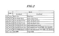
- FIG. 1 is a circuit configuration diagram showing an embodiment of a successive approximation AD converter circuit according to the present invention. It is a state explanatory view showing a node potential state inside the comparator of the AD conversion circuit of the embodiment. It is a circuit block diagram which shows the structural example of the comparator in the 1st modification of the AD converter circuit of embodiment. It is a circuit block diagram which shows the structural example of the comparator in the 2nd modification of the AD converter circuit of embodiment. It is a circuit block diagram which shows the structural example of the comparator in the 3rd modification of the AD converter circuit of embodiment. It is a circuit block diagram which shows the structural example of the comparator in the 4th modification of the AD converter circuit of embodiment.
- FIG. 3 is a circuit configuration diagram showing a second embodiment of a successive approximation AD converter circuit according to the present invention.
- FIG. 6 is a circuit configuration diagram showing a state of each changeover switch SW0 to SWn-1 in a comparison determination period (hold period) of the successive approximation type AD converter circuit of the second embodiment. It is a circuit block diagram which shows the structural example of the conventional AD converter circuit provided with the chopper type comparator.
- FIG. 1 shows an embodiment of a successive approximation AD converter circuit according to the present invention.
- the AD conversion circuit shown in FIG. 1 is a sample and hold circuit that alternately samples an analog input Vin input to an analog input terminal IN and a comparison voltage Vref applied to a reference voltage terminal to hold a differential voltage.
- a chopper comparator CMP that amplifies the differential voltage sampled by the sample and hold circuit S & H
- a logic circuit LG that receives the output of the chopper comparator CMP and the sampling clock ⁇ s and outputs a predetermined signal
- the successive approximation register SAR for sequentially taking in the output of the logic circuit LG, and the sample-and-hold circuit as a comparison voltage Vref using a voltage obtained by DA-converting the output code of the SAR by switching an internal switch according to a signal output from the register SAR Local DA converter circuit DAC that outputs to S & H Is provided.
- the sample and hold circuit S & H includes a pair of sampling switches SS1 and SS2 that are complementarily turned on and off by a sampling clock ⁇ s and a clock / ⁇ s having a phase opposite to the sampling clock ⁇ s, a connection node of the switches SS1 and SS2, and the chopper comparator It comprises a sampling capacitor Cs connected between the CMP input terminals.
- the logic circuit LG includes an NOR gate G1 that receives the output of the chopper comparator CMP and the sampling clock ⁇ s and outputs a logical product of these signals, and an inverter G2 that inverts the output of the NOR gate G1. Become.
- the chopper comparator CMP includes three CMOS inverters INV1, INV2, and INV3 connected in cascade through capacitors C1 and C2, and switches S1, S2, and S3 that short-circuit the input / output terminals for each inverter. It is set as the provided structure.
- a feedback capacitor Cf is connected between the output terminal of the NOR gate G1 and the input terminal of the final stage inverter INV3.
- the NOR gate G1 is provided because the output of the inverter INV3 becomes an intermediate potential between the high level and the low level when the switch S3 is turned on during the sampling, so that it becomes a circuit in the subsequent stage (such as a successive approximation register). This is to prevent transmission.
- the switches S1, S2, and S3 are turned on during the sampling period, and the input and output of the inverters INV1, INV2, and INV3 are short-circuited.
- the potential is equal to the threshold value VLT. Therefore, in the sample and hold circuit S & H, the switch SS1 on the input terminal side is turned on by the sampling clock ⁇ s.
- the input analog voltage Vin is sampled in the sampling capacitor Cs with reference to VLT. That is, Cs is charged with a charge corresponding to the potential difference between VLT and Vin.
- the capacitors C1 and C2 are charged with voltages (VLT2-VLT1) and (VLT3-VLT2) which are the differences between the logic threshold values of the inverters.
- the reference side switch SS2 is turned on by the sampling clock / ⁇ s.
- the switches S1, S2 and S3 are turned off by ⁇ s and the input / output of the inverters INV1, INV2 and INV3 are cut off, so that each inverter operates as an amplifier and outputs according to the input potential. Change.
- the potential difference (Vref ⁇ Vin) is transmitted to the input terminal of the first-stage inverter INV1 through the sampling capacitor Cs, and the potential difference is gradually amplified by the inverters INV1, INV2, and INV3.
- the result of comparing the input analog voltage Vin and the comparison voltage Vref appears at the output of the inverter INV3.
- the logic threshold values of the inverters INV1, INV2, and INV3 are VLT1, VLT2, and VLT3
- the gains (amplification factors) are A1, A2, and A3
- the power supply voltage is Vdd
- the potentials (1) to (8) are as shown in FIG. As shown in FIG. 2, when Vin is higher than Vref, the output of the inverter INV3 is low level (ground potential GND), and when Vin is lower than Vref, the output of the inverter INV3 is high level (power supply voltage Vdd). I understand.
- the feedback capacitor Cf is connected between the output terminal of the NOR gate G1 and the input terminal of the inverter INV3 in the final stage, if the output potential of the NOR gate G1 increases, the capacitance Cf The electric charge is distributed to C2 according to the capacitance ratio, so that positive feedback is applied to the input terminal of the inverter INV3, and the input potential becomes higher by ⁇ V than that without the capacitor Cf.
- a minute hysteresis of about 0.1 LSB can be added to the chopper type comparator CMP with a simple design change by adding only one capacitor.
- the hysteresis of the chopper type comparator used in the AD converter circuit is smaller than the LSB and larger than the thermal noise, switching of the output of the comparator due to the thermal noise can be prevented and the conversion accuracy can be increased.
- the ratio of C2 and Cf can be set based on the calculation result with the adjusted predetermined gain.
- the capacitance may be added to either one of INV1 and INV2, or may be added to both, but adding to INV1 has a great effect on noise reduction in the comparator CMP.
- the transfer conductance of the MOS transistor is gm
- the threshold voltage is Vth
- the output resistance is r0
- the early voltage is VA
- the gate-source voltage is Vgs
- the drain-source voltage is Vds
- the drain current is Ids
- (VA + Vds) / (Vgs-Vth) .Ids 2 (VA + Vds) / (Vgs-Vth) (2) It is represented by In this equation, (Vgs ⁇ Vth) in the denominator is an effective voltage applied to the gate of the MOS transistor, and the effective voltage is larger as the power supply voltage Vdd is higher, and the effective voltage is smaller as Vdd is lower. Therefore, it can be seen from the above formula (2) that the gain increases as the power supply voltage Vdd increases and the effective voltage increases, and the gain decreases as the power supply voltage Vdd decreases and the effective voltage decreases.
- the hysteresis increases as the voltage Vdd is higher and the inverter gain is larger from the equation (1), and the hysteresis is smaller as the voltage Vdd is lower and the inverter gain is smaller. Further, the gain of the inverter increases as the gain of the MOS transistor increases. Therefore, it can be said that the comparator of the above embodiment, in which the hysteresis becomes larger as the power supply voltage is higher in accordance with the fluctuation of the power supply voltage, is suitable for an AD conversion circuit used in a system having a large power supply voltage fluctuation.
- FIG. 3 to 6 show modified examples of the comparator of the above embodiment.
- FIG. 3 shows the position where the positive feedback is applied from the output side as the input node of the second-stage inverter INV2
- FIG. 4 shows the position where the positive feedback is applied from the output side as the input node of the first-stage inverter INV1. It is a thing. Thus, even if the position where the positive feedback is applied is changed, substantially the same effect as the embodiment of FIG. 1 can be obtained.
- the feedback capacitance Cf needs to be smaller in FIG. 3 than in FIG. 1 and smaller in FIG. 4 than in FIG. Further, in FIG. 3, feedback is applied by a signal (9) having a phase opposite to that of FIG. 1, and in FIG. 4, feedback is applied by a signal (8) having the same phase as that of FIG.
- FIG. 5 shows a configuration in which positive feedback is applied to the input terminal of the second-stage inverter INV2 from the output side when the comparator CMP is configured by the two-stage inverters INV1 and INV2.
- a positive feedback may be applied to the input terminal of the first-stage inverter INV1.
- the capacitance value of Cf is made smaller than when positive feedback is applied to the third-stage inverter as shown in FIG. There is a need (for example 1/1000). In that case, it is expected that Cf cannot be composed of an element having the same structure as C2, but such a small Cf can be constructed by utilizing the capacitance between wirings.
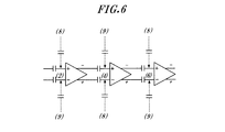
- FIG. 6 shows how feedback is applied when the comparator CMP is configured with three differential amplification stages.
- (8) means feedback by a signal in phase with the output of the NOR gate G1 in FIG. 1
- (9) means feedback by a signal in phase opposite to the output of the NOR gate G1 in FIG. Yes.
- FIG. 6 shows a state in which positive feedback is applied to both differential signals, a configuration may be adopted in which positive feedback is applied to only one of the differential signals.
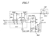
- FIG. 7 shows a second embodiment of the successive approximation AD converter circuit according to the present invention.
- a DA conversion circuit combining a charge distribution type and a resistance voltage division type is used as a local DA conversion circuit, and positive feedback is applied to the input terminal of the first-stage inverter INV1.
- the local DA conversion circuit in the present embodiment corresponds to a circuit having both functions of the sample and hold circuit S & H and the local DA conversion circuit DAC in the embodiment of FIG.
- the local DA converter circuit DAC in this embodiment includes a capacitor array including weighted capacitors C0, C1,... Cn-1 having a weight of 2n and a ladder resistor RLD including series resistors R1 to Rn. Have.
- the resistors R1 to Rn are normally set to the same resistance value.
- One terminals of the weight capacitors C0, C1,... Cn-1 are connected in common and connected to the input terminal of the first-stage inverter INV1 of the comparator CMP.
- One of the reference voltages Vref_h, Vref_l or the input voltage Vin is applied to the other terminal of C1,... Cn-1 among the weight capacitors C0, C1,. Made possible.
- either the selection voltage of the ladder resistor RLD or the input voltage Vin can be applied to the other terminal of the weight capacitor C0 by the changeover switch SW0.
- the sum of the weight capacitors C0, C1,... Cn-1 corresponds to the sampling capacitor Cs in FIG.
- a ground potential may be used as the reference voltage Vref_l.
- a voltage range FSR Full Scale Range
- the ladder resistor RLD is provided with switches S0, S1,... Sn for extracting the potential of each node of the ladder resistor.
- the changeover switches SW0 to SWn-1 are controlled by the upper bits of the successive approximation register SAR, and the switches S0 to Sn are controlled by the lower bits of the register SAR. Specifically, when the potential of the ladder resistor RLD is used by the lower bit of the SAR, any one of the switches S0 to Sn-1 is turned on, and the changeover switches SW0 to SWn-1 are only SW0. SW1 to SWn-1 do not operate.
- the switch S0 or Sn When using the weight capacitors C0, C1,... Cn-1, the switch S0 or Sn is turned on, the switches S1 to Sn or S0 to Sn-1 are turned off, and the reference voltage Vref_h or Vref_l is switched. It is transmitted to the capacitor C0 via the switch SW0.
- SW1 to SWn-1 are connected to the Vin input terminal at the time of sampling, and are connected to the reference voltage Vref_h or Vref_l according to the upper bit of the register SAR at the time of comparison determination.
- connection terminals of the changeover switches SW0 to SWn-1 are determined according to the value of the successive approximation register SAR and the sampling clock.
- FIG. 7 shows the state of each switch during the sampling period.
- the changeover switches SW0 to SWn-1 are all connected to the input voltage Vin at the other terminals of the corresponding weight capacitors C0, C1,. To charge the electric charge according to the potential of the input voltage.
- FIG. 8 shows the states of the change-over switches SW0 to SWn-1 during the comparison determination period (hold period).
- the change-over switches SW1 to SWn-1 in the comparison determination period are either Vref_h or Vref_l.
- the changeover switch SW0 is a selection voltage of the ladder resistor RLD, and which node voltage is selected is determined by the switches S1 to Sn.
- One of the reference voltages Vref_h and Vref_l is applied to the other terminals of the weight capacitors C0, C1,... Cn-1 during the comparison determination period, so that the applied voltage and the input voltage applied immediately before are applied. Charges corresponding to the potential difference from Vin remain and are distributed among C0, C1,... Cn-1, and the voltage generated at the common connection node is supplied to the input terminal of the inverter INV1 as a comparator.
- the switch S1 is turned on during the sampling period and the input / output of the inverter INV1 is short-circuited, so that the input potential and the output potential become equal to the logical threshold value VLT of the inverter.
- the input analog voltage Vin is sampled to the weighting capacitors C0, C1,. That is, a charge corresponding to the potential difference between VLT and Vin is charged.
- the selector switches SW0 to SWn-1 are connected to the reference voltage Vref_h or Vref_l according to the value of the register SAR.
- the potential corresponding to the potential difference between the input analog voltage sampled immediately before and the comparison voltage determined by the state of the changeover switches SW0 to SWn-1 is supplied to the input terminal of the inverter INV1.
- the switch S1 since the switch S1 is turned off and the input terminal and the output terminal of the inverter INV are disconnected, the inverter works as an amplifier to amplify and output the input potential.
- the reference voltage Vref_h is applied to one terminal of the ladder resistor RLD and the reference voltage Vref_l is applied to the other terminal of the ladder resistor RLD, and the potential difference is divided by the resistance ratio. These voltages are taken out by switches S0 to Sn controlled by the lower bits of the register SAR.
- the DA converter for example, 10 bits, required capacity of 2 10 times the minimum capacitance C0 in the case of only the charge distribution type (about 1000 times)
- either of the series resistors Rf1 and Rf2 in parallel with the resistor Rn and the potential of the connection node of Rf1 and Rf2 or the reference voltage Vref_l is selected.
- a switch SWf that is applied to one terminal of the capacitor Cf is provided.
- the switch SWf is controlled by the output of the NOR gate G1, and when it is high level, the potential of the connection node between Rf1 and Rf2 is applied to Cf, and when it is low level, the reference voltage Vref_l is applied to Cf.
- the combined resistance value of the resistors Rn and Rf1 and Rf2 is set to be the same resistance value as the other resistors R0 to Rn-1, and the resistance ratio of the resistors Rf1 and Rf2 depends on the amount of hysteresis to be added. For example, the ratio is set to 9: 1.
- the capacitance value of Cf is the same value as the smallest capacitance C0 among the weighting capacitances. This gives a hysteresis of 1/10 of 1LSB. Furthermore, by setting the capacitance value of Cf to a value smaller than the minimum weight capacitance C0, a smaller hysteresis can be given. In the embodiment of FIG.
- resistors Rf1 and Rf2 for applying a potential applied to the feedback capacitor Cf are provided in parallel with the resistor Rn of the ladder resistor RLD. However, if the resistance value is set appropriately, the resistors Rf1 and Rf2 are provided. Can be provided in parallel with the resistors Rn-1 and Rn.
- the present invention is not limited to the above embodiment.
- a comparator in which three stages of CMOS inverters are cascade-connected is shown, but a comparator in which two inverters are cascade-connected or a single inverter may be used.
- the feedback capacitor Cf is connected between the output terminal of the NOR gate G1 following the comparator CMP and the input terminal of one of the CMOS inverters.
- a switch element may be connected in series with the input terminal of the CMOS inverter and a predetermined constant potential point, and this switch element may be turned on and off by the output of the NOR gate G1 to provide positive feedback. Good. It is also possible to use a NAND gate instead of the NOR gate.
- CMOS inverter constituting a chopper type comparator.
- P-MOS, N-MOS on / off control transistors
- An inverter may be used to reduce the power consumption by controlling the operation timing.
- the present invention can be used for a chopper type comparator and an AD conversion circuit having the same.
Landscapes
- Physics & Mathematics (AREA)
- Nonlinear Science (AREA)
- Analogue/Digital Conversion (AREA)
- Manipulation Of Pulses (AREA)
Abstract
Description
この発明の他の目的は、チョッパ型コンパレータを備えたAD変換回路において、コンパレータに1LSB以下のヒステリシス特性を持たせることで、ヒステリシス付与に伴う変換誤差の増加を抑制できるようにすることにある。
Vhys=Vdd・Cf/(C2+Cf)・A1・A2 ……(1)
で表わすことができる。
Vhys=Vdd・Cf/(C2+Cf)・50・50=Vdd/10・210
より、Cf/(C2+Cf)≒1/4となるので、C2:Cf≒3:1程度に設定すれば良いことが分かる。
また、図1において、インバータINV1とINV2のそれぞれの入出力間に容量を付加して、インバータINV1,INV2のゲインを調整する構成とすることもできる。この場合には、調整した所定のゲインによる計算結果をもとにC2とCfの比率の設定ができる。容量はINV1,INV2のどちらか一方に付加してもよく、両方に付加しても良いが、INV1に付加した方がコンパレータCMPでのノイズ低減に大きな効果がある。
r0=(VA+Vds)/Ids
gm=2Ids/(Vgs-Vth)
より、MOSトランジスタのゲインG(=gm・r0)は、
G=2Ids・(VA+Vds)/(Vgs-Vth)・Ids
=2(VA+Vds)/(Vgs-Vth) ……(2)
で表わされる。この式において、分母の(Vgs-Vth)はMOSトランジスタのゲートにかかる実効電圧であり、この実効電圧は電源電圧Vddが高いほど大きく、Vddが低いほど実効電圧は小さくなる。従って、上記式(2)より、電源電圧Vddが高くなって実効電圧が大きくなるほどゲインは大きくなり、電源電圧Vddが低くなって実効電圧が小さくなるほどゲインは小さくなることが分かる。
CMP コンパレータ
SAR 逐次比較レジスタ
DAC ローカルDA変換回路
LG 論理回路
S1,S2,S3 短絡用スイッチ
C1,C2 容量
Cf フィードバック容量
RLD ラダー抵抗
C0~Cn-1 重み容量
SW0~SWn-1 切替えスイッチ
Claims (5)
- 入力アナログ電圧と比較電圧の大小を判定する比較回路と、該比較回路の判定結果を順次取り込んで保持するレジスタと、該レジスタの値を電圧に変換し前記比較電圧とするローカルDA変換回路と、を備えた逐次比較型AD変換回路であって、
前記比較回路は、
1または2以上の増幅段と、前記増幅段のうちいずれかの増幅段の入力端子に接続されたフィードバック容量とを有し、
第1の期間に入力アナログ電圧を取り込み、
第2の期間に、前記入力アナログ電圧と前記比較電圧との電位差に応じた電圧が入力されて、該入力電圧を前記増幅段で増幅し、
当該比較回路の出力が変化するとき、前記フィードバック容量を介して対応する増幅段の入力端子に正帰還をかけて1LSB以下のヒステリシスを付与するように構成したことを特徴とする逐次比較型AD変換回路。 - 前記ヒステリシスが1LSBの1/2以下の大きさとなるようにフィードバック容量の容量値が決定されていることを特徴とする請求項1に記載の逐次比較型AD変換回路。
- 前記比較回路は縦続接続された2以上の増幅段を有し、前記フィードバック容量を介して対応する入力端子に正帰還をかける増幅段は最終段の増幅段であることを特徴とする請求項1または2に記載の逐次比較型AD変換回路。
- 前記比較回路は、
CMOSインバータを前記増幅段として有するとともに、各CMOSインバータの入出力端子間にそれぞれ設けられたスイッチ素子と、前記CMOSインバータ間に設けられた容量と、を有し、
第1の期間に前記スイッチ素子がオン状態にされて、サンプリング容量の一方の端子に前記CMOSインバータの論理しきい値に相当する電圧が印加されて該電圧を基準に入力アナログ電圧を取り込み、
第2の期間に、前記サンプリング容量に前記入力アナログ電圧と前記比較電圧との電位差に応じた電荷がチャージされ、かつ前記スイッチ素子がオフ状態にされて前記サンプリング容量の電位を前記CMOSインバータで増幅し、
当該比較回路の出力が変化するとき、前記フィードバック容量を介して対応するCMOSインバータの入力端子に正帰還をかけるように構成されていることを特徴とする請求項1~3のいずれかに記載の逐次比較型AD変換回路。 - 前記比較回路の後段には、該比較回路の最終増幅段の出力と前記サンプリングのタイミング与えるクロック信号とを入力とする論理ゲートが設けられ、該論理ゲートの出力もしくはそれを反転した信号によって前記フィードバック容量の一方の端子の電位が変化され、対応するCMOSインバータの入力端子に正帰還をかけるように構成されていることを特徴とする請求項4に記載の逐次比較型AD変換回路。
Priority Applications (2)
| Application Number | Priority Date | Filing Date | Title |
|---|---|---|---|
| CN2009801433981A CN102204107A (zh) | 2008-10-30 | 2009-09-02 | 逐次逼近型ad转换电路 |
| US13/126,863 US20110205099A1 (en) | 2008-10-30 | 2009-09-02 | Successive approximation type a/d converter circuit |
Applications Claiming Priority (2)
| Application Number | Priority Date | Filing Date | Title |
|---|---|---|---|
| JP2008279340A JP2010109660A (ja) | 2008-10-30 | 2008-10-30 | 逐次比較型ad変換回路 |
| JP2008-279340 | 2008-10-30 |
Publications (1)
| Publication Number | Publication Date |
|---|---|
| WO2010050293A1 true WO2010050293A1 (ja) | 2010-05-06 |
Family
ID=42128661
Family Applications (1)
| Application Number | Title | Priority Date | Filing Date |
|---|---|---|---|
| PCT/JP2009/065331 Ceased WO2010050293A1 (ja) | 2008-10-30 | 2009-09-02 | 逐次比較型ad変換回路 |
Country Status (4)
| Country | Link |
|---|---|
| US (1) | US20110205099A1 (ja) |
| JP (1) | JP2010109660A (ja) |
| CN (1) | CN102204107A (ja) |
| WO (1) | WO2010050293A1 (ja) |
Cited By (1)
| Publication number | Priority date | Publication date | Assignee | Title |
|---|---|---|---|---|
| CN102904573A (zh) * | 2011-07-29 | 2013-01-30 | 联发科技(新加坡)私人有限公司 | 模数转换器及模数转换方法 |
Families Citing this family (18)
| Publication number | Priority date | Publication date | Assignee | Title |
|---|---|---|---|---|
| US8754798B2 (en) * | 2011-12-21 | 2014-06-17 | Realtek Semiconductor Corp. | High-speed successive-approximation-register analog-to-digital converter and method thereof |
| CN104283562A (zh) * | 2013-07-12 | 2015-01-14 | 上海明波通信技术股份有限公司 | 逐次逼近型模数转换装置 |
| CN104348485B (zh) * | 2013-08-06 | 2017-09-15 | 博通集成电路(上海)有限公司 | 模数转换器和将模拟信号转换为数字信号的方法 |
| JP5811153B2 (ja) * | 2013-09-20 | 2015-11-11 | 株式会社デンソー | A/d変換装置 |
| TWI521887B (zh) * | 2013-12-06 | 2016-02-11 | 碩頡科技股份有限公司 | 連續近似式類比數位轉換器 |
| US9679509B2 (en) * | 2014-05-01 | 2017-06-13 | Samsung Display Co., Ltd. | Positive feedback enhanced switching equalizer with output pole tuning |
| JP6641859B2 (ja) * | 2015-10-06 | 2020-02-05 | セイコーエプソン株式会社 | 振動デバイス、発振器、電子機器、および移動体 |
| JP6736871B2 (ja) * | 2015-12-03 | 2020-08-05 | セイコーエプソン株式会社 | 回路装置、発振器、電子機器及び移動体 |
| CN106569162B (zh) * | 2016-10-17 | 2019-04-02 | 深圳市鼎阳科技有限公司 | 一种逻辑分析仪探头的模拟带宽测量方法与装置 |
| JP6899686B2 (ja) * | 2017-03-31 | 2021-07-07 | エイブリック株式会社 | 差動増幅装置 |
| JP7200476B2 (ja) * | 2017-12-28 | 2023-01-10 | セイコーエプソン株式会社 | 回路装置、振動デバイス、電子機器及び移動体 |
| CN108336996A (zh) * | 2017-12-29 | 2018-07-27 | 成都华微电子科技有限公司 | 基于反相器设计的采样保持电路 |
| CN108347249A (zh) * | 2018-02-05 | 2018-07-31 | 华南理工大学 | 一种低功耗逐次逼近型模数转换电路及其控制方法 |
| US10917105B1 (en) * | 2018-08-29 | 2021-02-09 | Shenzhen Goodix Techology Co., Ltd | Successive approximation analog-to-digital converter with nonlinearity compensation |
| WO2020155063A1 (zh) | 2019-01-31 | 2020-08-06 | 深圳市汇顶科技股份有限公司 | 电流抵消电路、心率检测装置和可穿戴设备 |
| CN110928830A (zh) * | 2019-12-04 | 2020-03-27 | 能科科技股份有限公司 | 一种数据的采集方法、装置、计算机设备和存储介质 |
| CN111147076B (zh) * | 2019-12-31 | 2021-10-29 | 清华大学 | 可抵消采样噪声的模数转换器 |
| CN111786660B (zh) * | 2020-07-16 | 2022-07-22 | 中国电子科技集团公司第二十四研究所 | 一种斩波稳零比较电路 |
Citations (2)
| Publication number | Priority date | Publication date | Assignee | Title |
|---|---|---|---|---|
| JPH0537376A (ja) * | 1991-08-02 | 1993-02-12 | Nec Ic Microcomput Syst Ltd | Ad変換器 |
| JP2005269611A (ja) * | 2004-02-20 | 2005-09-29 | Rohm Co Ltd | 比較器、ad変換回路、半導体装置、および撮像装置 |
Family Cites Families (9)
| Publication number | Priority date | Publication date | Assignee | Title |
|---|---|---|---|---|
| US5617053A (en) * | 1993-06-17 | 1997-04-01 | Yozan, Inc. | Computational circuit |
| CN1109404C (zh) * | 1993-09-20 | 2003-05-21 | 株式会社鹰山 | 计算电路 |
| JP3737346B2 (ja) * | 2000-08-28 | 2006-01-18 | シャープ株式会社 | サンプルホールド増幅回路とそれを用いたパイプライン型ad変換器およびパイプライン型da変換器 |
| US6912139B2 (en) * | 2002-11-14 | 2005-06-28 | Fyre Storm, Inc. | Multi-channel control methods for switched power converters |
| JP3902778B2 (ja) * | 2004-01-07 | 2007-04-11 | 株式会社半導体理工学研究センター | アナログディジタル変換回路 |
| JP3839027B2 (ja) * | 2004-04-09 | 2006-11-01 | Necエレクトロニクス株式会社 | Ad変換器 |
| JP3968529B2 (ja) * | 2004-04-21 | 2007-08-29 | ソニー株式会社 | 差動増幅器、2段増幅器、及びアナログ/ディジタル変換器 |
| CN101128980B (zh) * | 2005-02-24 | 2016-03-30 | 密克罗奇普技术公司 | 分辨率对采样与保持信道的数目可互换的模拟-数字转换器 |
| US7504977B2 (en) * | 2007-04-23 | 2009-03-17 | Texas Instruments Incorporated | Hybrid delta-sigma/SAR analog to digital converter and methods for using such |
-
2008
- 2008-10-30 JP JP2008279340A patent/JP2010109660A/ja active Pending
-
2009
- 2009-09-02 CN CN2009801433981A patent/CN102204107A/zh active Pending
- 2009-09-02 WO PCT/JP2009/065331 patent/WO2010050293A1/ja not_active Ceased
- 2009-09-02 US US13/126,863 patent/US20110205099A1/en not_active Abandoned
Patent Citations (2)
| Publication number | Priority date | Publication date | Assignee | Title |
|---|---|---|---|---|
| JPH0537376A (ja) * | 1991-08-02 | 1993-02-12 | Nec Ic Microcomput Syst Ltd | Ad変換器 |
| JP2005269611A (ja) * | 2004-02-20 | 2005-09-29 | Rohm Co Ltd | 比較器、ad変換回路、半導体装置、および撮像装置 |
Cited By (1)
| Publication number | Priority date | Publication date | Assignee | Title |
|---|---|---|---|---|
| CN102904573A (zh) * | 2011-07-29 | 2013-01-30 | 联发科技(新加坡)私人有限公司 | 模数转换器及模数转换方法 |
Also Published As
| Publication number | Publication date |
|---|---|
| CN102204107A (zh) | 2011-09-28 |
| JP2010109660A (ja) | 2010-05-13 |
| US20110205099A1 (en) | 2011-08-25 |
Similar Documents
| Publication | Publication Date | Title |
|---|---|---|
| WO2010050293A1 (ja) | 逐次比較型ad変換回路 | |
| JP3902778B2 (ja) | アナログディジタル変換回路 | |
| US10135457B2 (en) | Successive approximation register analog-digital converter having a split-capacitor based digital-analog converter | |
| US7515086B2 (en) | Pipelined analog-to-digital converter and method of analog-to-digital conversion | |
| US7233275B2 (en) | Analog-to-digital converter with input signal range greater than supply voltage and extended dynamic range | |
| US8344930B2 (en) | Successive approximation register analog-to-digital converter | |
| US20130169454A1 (en) | System and Method for a Successive Approximation Analog to Digital Converter | |
| US7345530B1 (en) | Regulated switch driving scheme in switched-capacitor amplifiers with opamp-sharing | |
| US20100194614A1 (en) | MULTIPLYING DIGITAL-TO-ANALOG CONVERTER FOR High SPEED AND LOW SUPPLY VOLTAGE | |
| CN102844987B (zh) | 流水线式a/d转换器和a/d转换方法、以及动态式差动放大器 | |
| CN106257837B (zh) | 用于测试差分模/数转换器的方法及其对应系统 | |
| US20030117308A1 (en) | Pseudo-differential amplifier and analog-to-digital converter using the same | |
| US9413377B1 (en) | Switched capacitor circuit and compensation method thereof, and analog to digital converter | |
| EP1398880A2 (en) | Analog-digital conversion circuit | |
| US7333039B2 (en) | Dual mode sample and hold circuit and cyclic pipeline analog to digital converter using the same | |
| JP2010109661A (ja) | チョッパ型電圧比較回路および逐次比較型ad変換回路 | |
| WO2010038575A1 (ja) | 逐次比較型ad変換回路および制御用半導体集積回路 | |
| Chow et al. | 1V 10-bit successive approximation ADC for low power biomedical applications | |
| US20040189374A1 (en) | Bias voltage generating circuit, amplifier circuit, and pipelined AD converter capable of switching current driving capabilities | |
| JP4117976B2 (ja) | サンプルホールド回路 | |
| JPH0983316A (ja) | コンパレータおよびアナログ−デジタル変換回路 | |
| JP5853940B2 (ja) | 信号処理回路 | |
| JP2004260263A (ja) | Ad変換器 | |
| JP2005057717A (ja) | チョッパー型コンパレータ回路 | |
| CN119154879B (zh) | 一种高桥接电容匹配度的模数转换器及模数转换器电路 |
Legal Events
| Date | Code | Title | Description |
|---|---|---|---|
| WWE | Wipo information: entry into national phase |
Ref document number: 200980143398.1 Country of ref document: CN |
|
| 121 | Ep: the epo has been informed by wipo that ep was designated in this application |
Ref document number: 09823406 Country of ref document: EP Kind code of ref document: A1 |
|
| WWE | Wipo information: entry into national phase |
Ref document number: 13126863 Country of ref document: US |
|
| NENP | Non-entry into the national phase |
Ref country code: DE |
|
| 122 | Ep: pct application non-entry in european phase |
Ref document number: 09823406 Country of ref document: EP Kind code of ref document: A1 |