WO2010035404A1 - 化学的機械研磨装置、化学的機械研磨方法及び制御プログラム - Google Patents
化学的機械研磨装置、化学的機械研磨方法及び制御プログラム Download PDFInfo
- Publication number
- WO2010035404A1 WO2010035404A1 PCT/JP2009/004114 JP2009004114W WO2010035404A1 WO 2010035404 A1 WO2010035404 A1 WO 2010035404A1 JP 2009004114 W JP2009004114 W JP 2009004114W WO 2010035404 A1 WO2010035404 A1 WO 2010035404A1
- Authority
- WO
- WIPO (PCT)
- Prior art keywords
- semiconductor substrate
- polishing pad
- chemical mechanical
- mechanical polishing
- polishing
- Prior art date
- Legal status (The legal status is an assumption and is not a legal conclusion. Google has not performed a legal analysis and makes no representation as to the accuracy of the status listed.)
- Ceased
Links
Images




Classifications
-
- H—ELECTRICITY
- H10—SEMICONDUCTOR DEVICES; ELECTRIC SOLID-STATE DEVICES NOT OTHERWISE PROVIDED FOR
- H10P—GENERIC PROCESSES OR APPARATUS FOR THE MANUFACTURE OR TREATMENT OF DEVICES COVERED BY CLASS H10
- H10P52/00—Grinding, lapping or polishing of wafers, substrates or parts of devices
- H10P52/40—Chemomechanical polishing [CMP]
- H10P52/403—Chemomechanical polishing [CMP] of conductive or resistive materials
-
- H—ELECTRICITY
- H10—SEMICONDUCTOR DEVICES; ELECTRIC SOLID-STATE DEVICES NOT OTHERWISE PROVIDED FOR
- H10P—GENERIC PROCESSES OR APPARATUS FOR THE MANUFACTURE OR TREATMENT OF DEVICES COVERED BY CLASS H10
- H10P52/00—Grinding, lapping or polishing of wafers, substrates or parts of devices
-
- B—PERFORMING OPERATIONS; TRANSPORTING
- B24—GRINDING; POLISHING
- B24B—MACHINES, DEVICES, OR PROCESSES FOR GRINDING OR POLISHING; DRESSING OR CONDITIONING OF ABRADING SURFACES; FEEDING OF GRINDING, POLISHING, OR LAPPING AGENTS
- B24B37/00—Lapping machines or devices; Accessories
- B24B37/04—Lapping machines or devices; Accessories designed for working plane surfaces
-
- H—ELECTRICITY
- H10—SEMICONDUCTOR DEVICES; ELECTRIC SOLID-STATE DEVICES NOT OTHERWISE PROVIDED FOR
- H10D—INORGANIC ELECTRIC SEMICONDUCTOR DEVICES
- H10D64/00—Electrodes of devices having potential barriers
- H10D64/01—Manufacture or treatment
- H10D64/011—Manufacture or treatment of electrodes ohmically coupled to a semiconductor
Definitions
- the present invention relates to a chemical mechanical polishing apparatus, a chemical mechanical polishing method, and a control program used in a damascene process for forming a buried copper wiring in an interlayer insulating film made of an organic low-k film.
- a metal film such as Al deposited on the insulating film is processed by lithography and dry etching to form a metal wiring pattern, but the electromigration resistance of the Al wiring is low.
- the electrical resistance is relatively high and wiring delay occurs. For this reason, recently, a damascene process for copper wiring has been adopted for the multilayer wiring forming process.
- a low dielectric constant ( Employing low-k) membranes is essential.
- inorganic materials such as SiOF films and porous films have been studied, but organic materials such as fluororesins and amorphous fluorocarbons that can obtain a relative dielectric constant of 2.5 or less are also greatly used. Promising.
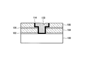
- an etch stop film 102, 106 made of, for example, SiCN, and an organic system made of, for example, amorphous fluorocarbon, are formed on the semiconductor wafer 100 formed up to the lower layer wiring (not shown).
- the low-k films 104 and 108 are laminated from the bottom in the order of 102 ⁇ 104 ⁇ 106 ⁇ 108 by the CVD (Chemical Vapor Deposition) method.
- the wiring groove 110 is formed in the upper low-k organic film 108, and the lower low-k organic film 102 has a via. Hole 112 is formed.
- irregularities corresponding to the wiring grooves 110 and the via holes 112 are formed on the surface of the semiconductor substrate 100.
- a barrier metal 114 made of, for example, TaN is formed on the surface of the semiconductor substrate 100 including the inside of the via hole 112 and the wiring groove 110 by the CVD method. Further, a copper seed layer (not shown) may be formed on the barrier metal 114 by sputtering.
- copper 116 is deposited on the surface of the semiconductor wafer 100 by electroplating so that the via hole 112 and the wiring groove 110 are filled.
- the uneven shape corresponding to the wiring groove 110 and the via hole 112 is reflected on the surface of the copper 116.
- the copper 116 on the semiconductor substrate 100 is flatly polished by chemical mechanical polishing (CMP), and as shown in FIG. 10E, the copper is only in the via hole 112 and the wiring groove 110. A buried copper wiring is formed leaving 116.
- CMP chemical mechanical polishing
- the damascene process described above is a dual damascene method in which the via hole 112 and the wiring groove 110 are simultaneously filled with a film of copper 116 to form a copper plug and a copper wiring at a time.
- the via hole 112 and the wiring groove 110 are separately filled with a film of copper 116 to form a copper plug and a copper wiring separately.
- a CMP process similar to the dual damascene method is performed.
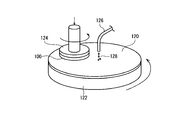
- FIG. 11 shows a conventional typical CMP apparatus.
- This CMP apparatus presses a rotary head (upper surface plate) 124 that fixes and holds the semiconductor wafer 100 against a rotary table (lower surface plate) 122 to which a polishing cloth or a polishing pad 120 is attached, thereby rotating the rotary head 120 and the rotating table 120.
- a slurry (abrasive) is supplied from the nozzle 126 onto the polishing pad 120, and the film on the lower surface (surface to be processed) of the semiconductor wafer 100 is shaved and planarized by chemical action and mechanical polishing.
- the present inventor has investigated the generation mechanism of scratches and dishing as described above.
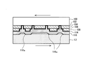
- the surface of the semiconductor wafer 100 surface to be processed
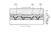
- FIG. 13 since the polishing pad 12 rubs in the opposite direction to a part, a large shear stress is applied to the copper 116 as the material to be polished, particularly to the convex portion 116a. It was found that small scratches were likely to occur, and when the slurry entered the small scratches, the portions were excessively shaved and developed into scratches and dishing.
- the copper to be polished is a relatively soft metal, and the low-k organic film that forms the interlayer insulation film is vulnerable to external stress and tends to accumulate shear stress, which can cause scratches during touchdown. This is thought to be the cause.
- the present invention has been made on the basis of the above-mentioned problems of the prior art and the investigation of the cause thereof, and is a copper deposited on an interlayer insulating film composed of an organic low-k film in a damascene process.
- a chemical mechanical polishing apparatus, a chemical mechanical polishing method and a control program that prevent formation of scratches and dishing during polishing and enable formation of embedded copper wiring with excellent flatness accuracy and electrical property stability. provide.
- a chemical mechanical polishing method for forming a copper wiring in a copper wiring damascene process using an organic film having a low dielectric constant (low-k organic film) as an interlayer insulating film on a semiconductor substrate A chemical mechanical polishing method for polishing copper deposited on an organic film, wherein the polishing is performed over substantially the entire surface to be processed of the semiconductor substrate while spinning the semiconductor substrate and the polishing pad in the same direction.
- the polishing pad in the first step, is prevented from rubbing in the reverse direction over substantially the entire surface to be processed of the semiconductor substrate while rotating the semiconductor substrate and the polishing pad in the same direction. Since both are brought into contact with each other, the shear stress applied to the surface copper is small at any part of the surface to be treated, and the degree of the shear stress accumulating in the underlying low-k organic film is also small. As a result, it is possible to start polishing copper without causing scratches that become seeds for scratching or dishing over substantially the entire surface to be processed on the substrate.
- a chemical mechanical polishing method for forming a copper wiring according to a second aspect of the present invention is deposited on the organic film in a damascene process of a copper wiring using an organic film having a low dielectric constant as an interlayer insulating film on a semiconductor substrate.
- a chemical mechanical polishing method for polishing copper wherein the semiconductor substrate and the polishing pad are rotated in the same direction, the respective rotation center axes are aligned on a straight line, and both are brought into contact with each other. And supplying a slurry to a contact interface between the semiconductor substrate and the polishing pad, and chemically controlling copper on the semiconductor substrate by controlling a relative rotation speed and pressure between the semiconductor substrate and the polishing pad.
- a second step of mechanically polishing is deposited on the organic film in a damascene process of a copper wiring using an organic film having a low dielectric constant as an interlayer insulating film on a semiconductor substrate.
- the respective rotation center axes are brought into contact with each other while rotating the semiconductor substrate and the polishing pad in the same direction.
- the shear stress applied to the surface copper is small everywhere, and the degree of shear stress accumulation in the underlying low-k organic film is also small. As a result, it is possible to start polishing copper without causing scratches that become seeds for scratching or dishing over substantially the entire surface to be processed on the substrate.
- the rotational speed of each of the semiconductor substrate and the polishing pad in the first step may be appropriately set according to the diameter of the substrate, the uneven state of the copper surface, the material of the low-k organic film and the polishing pad, etc. You may set in the range of 50 rpm-300 rpm, for example, 80 rpm-90 rpm. Although the rotational speeds of the two may be different, the speed difference is preferably as small as possible in order to reduce the impact or stress at the time of contact, and the speed difference is most preferably made substantially zero.
- the semiconductor substrate and the polishing pad are the same. It is preferable that the polishing pad is not rubbed in the reverse direction over almost the entire surface of the semiconductor substrate to be processed, or the rotation center axis of the semiconductor substrate and the rotation center axis of the polishing pad are More preferably, they are aligned on a straight line.
- the axis and the rotation center axis of the polishing pad can be offset, and the offset position of the semiconductor substrate relative to the polishing pad can be varied. In this case, it is possible to increase the polishing efficiency by using a polishing pad having a sufficiently larger diameter than the semiconductor substrate.
- the relative rotational speed between the semiconductor substrate and the polishing pad may be appropriately set according to the diameter of the substrate, the uneven state of the copper surface, the material of the low-k organic film and the polishing pad, and the like.
- the relative rotational speed may be controlled by a method in which the rotational speed of the polishing pad is kept constant and the rotational speed of the semiconductor substrate is lower than the rotational speed in the first step, and the relative rotational speed is made variable. Also good. Further, the pressure applied to the contact interface is gradually increased.
- the pressure applied to the contact interface between the semiconductor substrate and the polishing pad may be arbitrarily controlled according to the above-mentioned conditions, but usually a method of gradually increasing is adopted. It's okay.
- the chemical mechanical polishing method of the present invention is a third aspect in which a semiconductor substrate and a polishing pad are rotated in the same direction while being separated in order to finish polishing copper on the semiconductor substrate.
- the process is further included.
- the polishing pad is not rubbed in the reverse direction over almost the entire surface of the semiconductor substrate, or the rotation center axis of the semiconductor substrate and the rotation center axis of the polishing pad are aligned. It is more preferable to arrange them in the same manner.
- a method of offsetting the rotation center axis of the semiconductor substrate and the rotation center axis of the polishing pad is also possible.
- the chemical mechanical polishing apparatus is for polishing copper deposited on an organic film in a damascene process of copper wiring using an organic film having a low dielectric constant as an interlayer insulating film on a semiconductor substrate.
- a first chemical mechanical polishing apparatus for holding a semiconductor substrate in a detachable manner and rotating the first surface plate, and a first surface plate for rotating the first surface plate at a desired rotational speed.
- a rotation driving unit a first surface plate configured to be rotatable with a polishing pad attached thereto, a second rotation driving unit for rotating the second surface plate at a desired rotation speed, and the first A first actuator for relatively separating or pressingly contacting the first surface plate and the second surface plate, and rotating the first surface plate and the second surface plate in the same direction.
- the polishing pad is reversed over substantially the entire surface to be processed of the semiconductor substrate.
- the first rotation drive unit, the second rotation drive unit, and the first rotation unit are brought into contact with each other without rubbing in the direction, and then the copper on the semiconductor substrate is chemically and mechanically polished.
- a slurry supply unit for supplying slurry to a contact interface between the semiconductor substrate and the polishing pad.
- a chemical mechanical polishing apparatus is for polishing copper deposited on an organic film in a damascene process of a copper wiring using an organic film having a low dielectric constant as an interlayer insulating film on a semiconductor substrate.
- a first chemical mechanical polishing apparatus for holding a semiconductor substrate in a detachable manner and rotating the first surface plate, and a first surface plate for rotating the first surface plate at a desired rotational speed.
- a rotation driving unit a first surface plate configured to be rotatable with a polishing pad attached thereto, a second rotation driving unit for rotating the second surface plate at a desired rotation speed, and the first
- a first actuator for relatively separating or pressingly contacting the first surface plate and the second surface plate, and rotating the first surface plate and the second surface plate in the same direction. While aligning each rotation center axis on a straight line, a controller for controlling the first rotation drive unit, the second rotation drive unit, and the first actuator so as to chemically and mechanically polish copper on the semiconductor substrate, and the semiconductor substrate
- a slurry supply unit for supplying the slurry to a contact interface with the polishing pad.
- a second actuator for moving the second platen relative to the first platen in a direction perpendicular to the rotation center axis is provided.
- a second actuator for moving the second platen relative to the first platen in a direction perpendicular to the rotation center axis is provided.
- control program of the present invention operates on a computer and, when executed, causes the computer to control the chemical mechanical polishing apparatus so that the chemical mechanical polishing method of the present invention is performed.
- the chemical mechanical polishing method or the control program of the present invention it is deposited on the interlayer insulating film made of an organic low-k film in the damascene process by the configuration and operation as described above. It is possible to prevent the occurrence of scratches and dishing during the polishing of copper and to form a buried copper wiring excellent in flatness accuracy and electrical property stability.
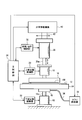
- FIG. 1 shows a main configuration of a CMP (Chemical Mechanical Polishing) apparatus according to an embodiment of the present invention.
- This CMP apparatus can be suitably used in a damascene process for forming a buried copper wiring.
- the CMP apparatus is deposited on the low-k organic film (interlayer insulating film) 108 of the semiconductor wafer 100 in the damascene process of FIG. It can be used in a CMP process (FIG. 10 (d) ⁇ (e)) for polishing the copper 116 flatly.
- a polishing pad 12 is attached to a rotating head (upper surface plate) 10 that can be rotated and moved up and down, and the semiconductor wafer 100 is faced up on a stationary rotating table (lower surface plate) 14 that can be rotated. Attach with.
- the rotary table 14 is provided with holding means, for example, a vacuum chuck (not shown) for detachably fixing the semiconductor wafer 100.
- the rotary head 10 is coupled to the rotary shaft 16 a of the upper motor 16, and the rotary table 14 is coupled to the rotary shaft 18 a of the lower motor 18.
- the rotation center axis of the rotary head 10 that is, the rotation axis 16a of the upper motor 16, and the rotation center axis of the rotary table 14, that is, the rotation axis 18a of the lower motor 18, are aligned on the same vertical line N.
- the head 10 and the rotary table 14 face each other directly in front.
- the upper surface plate control unit 20 and the lower surface plate control unit 22 have motor drive circuits that supply drive currents to the upper motor 16 and the lower motor 18, respectively, and the rotary head according to a control signal from the main control unit 24. 10 and the rotation operation (rotation start / stop, rotation speed, etc.) of the rotary table 14 are controlled.
- the rotary head 10 and the upper motor 16 are coupled to a drive shaft 28a of a lifting / pressurizing actuator 28 fixedly attached to a support base or frame 26.
- the elevating / pressurizing actuator 28 is composed of, for example, an air cylinder or a linear actuator with a built-in motor, and the drive shaft 28a is aligned on the vertical line N.
- the elevating / pressurizing control unit 30 has a pneumatic circuit or a driving circuit for supplying compressed air or driving current to the actuator 28, and controls the elevating and pressing force of the rotary head 10 according to instructions from the main control unit 24. To do.
- the slurry supply unit 32 has a tank for storing a slurry (abrasive) made of a polishing liquid containing, for example, alumina abrasive grains, and a pump for pumping and discharging the slurry from the tank. It is connected to one end of the slurry supply pipe 34. The other end of the slurry supply pipe 34 is connected to a slurry introducing portion (not shown) in the rotary head 10 via a rotary joint 36 attached to the rotary shaft 16 a of the upper motor 16. A slurry flow path (not shown) that leads from the slurry introduction portion to the polishing pad is also provided in the rotary head 10.
- a slurry (abrasive) made of a polishing liquid containing, for example, alumina abrasive grains
- the slurry sent from the slurry supply unit 32 is sent to the polishing pad 12 through the slurry supply pipe 34, the rotary joint 36, the slurry introduction unit in the rotary head 10, and the slurry flow path, and oozes out from the entire surface of the polishing pad 12. It is like that.
- the main control unit 24 includes a microcomputer, and according to software (program) stored in the external memory or the internal memory, each part in the apparatus, particularly the rotary head 10, the rotary table 14, the elevating / pressurizing actuator 28, and the slurry supply The individual operations of the unit 32 and the operation (sequence) of the entire apparatus are controlled.
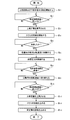
- FIG. 2 shows a main procedure of a control program executed by the main control unit 24 for the CPM process in the damascene process for forming the embedded copper wiring.
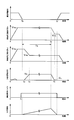
- FIG. 3 shows a temporal change (waveform) of the state or physical quantity of each part in this CMP process.
- the rotary head 10 In the initial state, as shown in FIG. 1, the rotary head 10 is located at the original position set above the rotary table 14, and the polishing pad 12 is separated from the semiconductor wafer 100 on the rotary table 14.
- the main control unit 24 first starts the upper motor 16 and the lower motor 18 through the upper surface plate control unit 20 and the lower surface plate control unit 22, respectively, and rotates the head (upper surface plate) 10 and the rotation table (lower surface plate) 14. Are raised to touch-down (contact) speeds V 10a and V 14a , respectively (steps S 1 and S 2 ).
- the upper surface plate control unit 20 and the lower surface plate control unit 22 use, for example, a rotation speed detector such as a rotary encoder (not shown) to control the rotation speeds of the polishing pad 12 and the rotary table 14 by a footback method. It is also possible to notify the main controller 24 of the state by a status signal or the like when the respective rotation speeds reach or become the set values V 10a and V 14a .
- a rotation speed detector such as a rotary encoder (not shown) to control the rotation speeds of the polishing pad 12 and the rotary table 14 by a footback method. It is also possible to notify the main controller 24 of the state by a status signal or the like when the respective rotation speeds reach or become the set values V 10a and V 14a .
- the main control unit 24 lowers the rotary head 10 by the lift / pressurization actuator 28 through the lift / pressurization control unit 30 (step S 3 ), and predetermined based on the descending distance or height position of the rotary head 10.
- the slurry supply unit 32 starts to send the slurry (step S 4 ).
- the slurry sent from the slurry supply unit 32 is sent to the polishing pad 12 through the slurry supply pipe 34, the rotary joint 36, the slurry introduction unit in the rotary head 10, and the slurry flow path, and is supplied to the polishing pad 12. It exudes from the entire surface.
- the main controller 24 checks the touch-down of the polishing pad 12 with respect to the semiconductor wafer 100 (Step S 5, time t 2).
- This touch-down confirmation may be based on, for example, the descending distance or height position of the rotary head 10, but usually a method of detecting a change in the rotational torque of the upper motor 16 is certain.
- FIG. 4 shows a state where the polishing pad 12 is in contact with or in contact with the semiconductor wafer 100.
- the main control unit 24 controls the relative rotational speed between the rotary head 10 and the rotary table 14 to a predetermined value suitable for polishing (step S 6 ).
- a predetermined value suitable for polishing For example, as shown in FIG. 3, the rotational speed of the rotary table 14 is set to be lower than the touch-down setting value V 14a while maintaining the rotational speed of the rotary head 10 at the touch-down setting value V 10a. The speed is linearly reduced to the value V 14b , and the relative rotational speed is linearly raised to the setting value V S for polishing (time t 3 to time t 4 ).
- the relative rotational speed setting value V S for polishing may be selected to an appropriate value, for example, 3 to 30 rpm according to the diameter of the semiconductor wafer 100, the surface irregularity state, the material of the polishing pad 12, etc., and is variable during polishing. It is also possible to control.
- the main control unit 24, the lifting / by the pressurization control unit 30 through the elevation / pressurizing actuator 28 controls the pressing force i.e. the polishing pressure of the polishing pad 12 with respect to the semiconductor wafer 100 (Step S 7), the normal processing time It gradually increases (for example, linearly) over time.
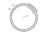
- the semiconductor wafer 100 and the polishing pad 12 are rotated in the same direction with their rotation centers aligned on the same straight line N as shown in FIG.
- the shear stress applied to the copper 116 is small at any part of the surface to be processed, and the degree of the shear stress accumulating in the underlying low-k organic films 108 and 104 is also small. For this reason, the polishing of the copper 116 can be started without causing scratches or dishing seeds on the entire surface of the semiconductor wafer 100.
- the relative rotation speed and the polishing are performed while the semiconductor wafer 100 and the polishing pad 12 are rotated in the same direction with the rotation center aligned on the same straight line N as shown in FIG. Since the pressure is gradually changed or adjusted, the polishing of the copper 116 can proceed stably without giving any sudden change of the shear stress to any part of the surface of the semiconductor wafer 100.
- step S 8 the time t 5
- the main controller 24 to terminate the polishing, the upper surface plate switching the rotary head 10 via the control unit 20 and the lower platen control section 22 of the relative rotational speed between the rotary table 14 to the rotational speed V E for separation (step S 9, S 10).
- V 10b V 14b
- the main controller 24 raises the rotary head 10 by the elevator / pressurization actuator 28 through the elevator / pressurization controller 30 to separate or separate the semiconductor wafer 100 and the polishing pad 12 (step S 11 , time point). t 7).
- the slurry supply unit 32 stops supplying the slurry (step S 12 ).
- the rotation of the rotary head 10 and the rotary table 14 is stopped through the upper surface plate control unit 20 and the lower surface plate control unit 22 (step S 13 ).
- both of them are rotated in the same direction with the rotation centers aligned on the same straight line N as shown in FIG. Since the semiconductor wafer 100 and the polishing pad 12 are smoothly separated by reducing (preferably 0), the surface of the semiconductor wafer 100 (the surface of the copper 116 and the surface of the low-k organic film 108) is damaged. The possibility can be reduced as much as possible.
- FIG. 7 shows a main configuration of the CMP apparatus according to the second embodiment. Parts having the same configuration or function as those of the CMP apparatus (FIG. 1) of the first embodiment described above are denoted by the same reference numerals.
- a semiconductor wafer 100 is mounted face-down on a rotary head (upper surface plate) 10, and a rotary table (lower surface plate) 14 whose diameter (diameter) is much larger than that of the rotary head 10, for example, about twice.
- a polishing pad 12 is affixed, and the rotation center axis of the rotary head 10 and the rotation center axis of the rotary table 14 are aligned on the same axis or can be arbitrarily offset.
- the elevating / pressurizing actuator 28 coupled to the rotary head 10 via the upper motor 16 can be moved in one horizontal direction (X direction), and is moved up and down by a horizontal moving mechanism 40 installed thereabove. / The pressure actuator 28 and thus the position of the rotary head 10 can be varied in the horizontal direction.
- the rotary head 10 is provided with holding means for detachably mounting the semiconductor wafer 100, such as a vacuum chuck (not shown).
- the slurry supply pipe 34 is connected to a slurry introducing portion (not shown) in the rotary table 14 via a rotary joint 36 attached to the rotary shaft 18 a of the lower motor 18.
- a slurry flow path (not shown) that leads from the slurry introduction portion to the polishing pad is provided in the rotary table 14.
- the slurry sent from the slurry supply unit 32 is sent to the polishing pad 12 through the slurry supply pipe 34, the rotary joint 36, the slurry introduction unit in the rotary table 14, and the slurry flow path, and oozes out from the entire surface of the polishing pad 12. It is like that.
- the respective rotation center axes are aligned and touched down. It can be performed.
- the polishing pad 12 is pressed against the surface (surface to be processed) of the semiconductor wafer 100 as shown in FIG. Since the pad 12 does not rub in the reverse direction, the shear stress applied to the surface copper 116 (particularly the convex portion 116a) is small, and the degree of the shear stress accumulating in the underlying low-k organic films 108 and 104 is also small. For this reason, the polishing of the copper 116 can be started without generating scratches that can cause scratches or dishing over the entire surface of the semiconductor wafer 100.
- the relative rotational speed between the rotary head 10 and the rotary table 14 is adjusted to the set value V S , and if a predetermined time has elapsed, preferably the convex portion 116a of the copper 116 on the semiconductor wafer 100 corresponds.
- the horizontal movement mechanism 40 is operated to shift the rotation center axis of the semiconductor wafer 100 from the rotation center axis of the polishing pad 12 as shown in FIG. 8, and the polishing process is performed at the offset position.
- the offset position of the rotary head 10 may be linearly moved in the direction of the arrow X with respect to the rotary table 14 (polishing pad 12), or the arrow ⁇ It may be moved in a ring shape in the direction.
- a portion where the polishing pad 12 rubs in the reverse direction and a portion where the polishing pad 12 rubs in the opposite direction are mixed in the surface (surface to be processed) of the semiconductor wafer 100.
- the convex portion 116a (FIG. 6) of the copper 116 of the film to be processed is considerably shaved and there is no scratch on the surface, there is little possibility that scratches or dishing will occur even if a certain amount of shear stress is applied thereto.
- the semiconductor wafer 100 When polishing is finished, the semiconductor wafer 100 can be separated from the polishing pad 12 at the offset position, but the rotary head 10 is returned to the center of the rotary table 14 and the relative rotational speed is reduced (preferably It is preferred to separate them from each other. As a result, the possibility of scratching the surface of the semiconductor wafer 100 (the surface of the copper 116 and the surface of the low-k organic film 108) at the end of polishing can be reduced as much as possible.
- FIG. 9 shows a configuration example of the main control unit 24 that controls each part of the CMP apparatus (FIGS. 1 and 7) and controls the entire sequence in order to perform the CMP processing method in the embodiment.
- the main control unit 24 of this configuration example includes a processor (CPU) 52, an internal memory (RAM) 54, a program storage device (HDD) 56, an external memory drive (DRV) such as a flash memory or an optical disk connected via a bus 50. 58, an input device (KEY) 60 such as a keyboard and a mouse, a display device (DIS) 62, a network interface (COM) 64, and a peripheral interface (I / F) 66.
- CPU central processing unit
- RAM random access memory
- HDD program storage device
- DVR external memory drive
- 58 an input device (KEY) 60 such as a keyboard and a mouse
- DIS display device
- COM network interface
- I / F peripheral interface
- the processor (CPU) 52 reads a code of a required program from a storage medium 68 such as a flash memory or an optical disk loaded in the external memory drive (DRV) 58 and stores it in the HDD 56. Alternatively, a required program can be downloaded from the network via the network interface 64. Then, the processor (CPU) 52 develops the code of a program necessary for each stage or each scene from the HDD 156 onto the working memory (RAM) 54, executes each step, performs necessary arithmetic processing, and performs a peripheral interface 66. Each part in the apparatus is controlled via All the programs for implementing the CMP method described in the above embodiment are executed by this computer system.
- a storage medium 68 such as a flash memory or an optical disk loaded in the external memory drive (DRV) 58
- a required program can be downloaded from the network via the network interface 64.
- the processor (CPU) 52 develops the code of a program necessary for each stage or each scene from the HDD 156 onto the working memory (RAM)
- FIG. 1 It is a figure which shows the main structures of the CMP apparatus in one Embodiment of this invention. It is a flowchart figure which shows the main procedures of the control program for the CPM process in embodiment. It is a wave form diagram which shows the time change of the state or physical quantity of each part in the CMP process of an embodiment. It is a figure which shows the state which has contacted or contacted the polishing pad with the semiconductor wafer in the CMP apparatus of embodiment. It is a top view which shows the rotation direction and relative positional relationship of a semiconductor wafer and a polishing pad in CMP of embodiment. It is a schematic sectional drawing which shows typically the mode of a contact interface just after a polishing pad contacted with a semiconductor wafer in CMP of an embodiment.
- FIG. 1 It is a figure which shows the main structures of the CMP apparatus in 2nd Embodiment. It is a top view which shows the rotation direction and relative positional relationship of the semiconductor wafer and polishing pad in 2nd Embodiment. It is a block diagram which shows the structural example of the main control part in the CMP apparatus of embodiment. It is a figure which shows the process of the damascene process of copper wiring which uses an organic-type low-k film
- Rotating head (upper surface plate) 12 Polishing pad 14 Rotary table (lower surface plate) DESCRIPTION OF SYMBOLS 16 Upper motor 18 Lower motor 20 Upper surface plate control part 22 Lower surface plate control part 24 Main control part 28 Lift / pressurization actuator 30 Lift / pressurization control part 32 Slurry supply part 32 Slurry supply pipe 36 Rotary joint 40 Horizontal movement mechanism 100 Semiconductor wafer 104, 108 low-k film (interlayer insulating film) 106 copper
Landscapes
- Engineering & Computer Science (AREA)
- Mechanical Engineering (AREA)
- Mechanical Treatment Of Semiconductor (AREA)
- Finish Polishing, Edge Sharpening, And Grinding By Specific Grinding Devices (AREA)
- Internal Circuitry In Semiconductor Integrated Circuit Devices (AREA)
Abstract
Description
12 研磨パッド
14 回転テーブル(下部定盤)
16 上部モータ
18 下部モータ
20 上部定盤制御部
22 下部定盤制御部
24 主制御部
28 昇降/加圧アクチエータ
30 昇降/加圧制御部
32 スラリ供給部
32 スラリ供給管
36 ロータリジョイント
40 水平移動機構
100 半導体ウエハ
104,108 low-k膜(層間絶縁膜)
106 銅
Claims (22)
- 半導体基板上の層間絶縁膜に誘電率の低い有機膜を用いる銅配線のダマシンプロセスにおいて前記有機膜上に堆積された銅を研磨するための化学的機械研磨方法であって、
半導体基板と研磨パッドとを同方向に回転させながら、前記半導体基板の被処理面の略全域で前記研磨パッドが逆方向に擦らないようにして両者を当接させる第1の工程と、
前記半導体基板と前記研磨パッドとの間の接触界面にスラリを供給し、前記半導体基板と前記研磨パッドとの間の圧力および相対回転速度を制御して前記半導体基板上の銅を化学的機械的に研磨する第2の工程と
を有する銅配線形成用の化学的機械研磨方法。 - 半導体基板上の層間絶縁膜に誘電率の低い有機膜を用いる銅配線のダマシンプロセスにおいて前記有機膜上に堆積された銅を研磨するための化学的機械研磨方法であって、
半導体基板と研磨パッドとを同方向に回転させながら、それぞれの回転中心軸を一直線上に揃えて、両者を当接させる第1の工程と、
前記半導体基板と前記研磨パッドとの間の接触界面にスラリを供給し、前記半導体基板と前記研磨パッドとの間の相対回転速度および圧力を制御して前記半導体基板上の銅を化学的機械的に研磨する第2の工程と
を有する銅配線形成用の化学的機械研磨方法。 - 前記第1の工程において、前記半導体基板および前記研磨パッドのそれぞれの回転速度を50rpm~300rpmの範囲内で設定する請求項1または請求項2に記載の化学的機械研磨方法。
- 前記第1の工程において、前記半導体基板および前記研磨パッドのそれぞれの回転速度を80rpm~90rpmに設定する請求項3に記載の化学的機械研磨方法。
- 前記第1の工程において、前記半導体基板の回転速度と前記研磨パッドの回転速度との差を実質的に零にする請求項1または請求項2に記載の化学的機械研磨方法。
- 前記第2の工程において、前記半導体基板と前記研磨パッドとを同方向に回転させる請求項1または請求項2に記載の化学的機械研磨方法。
- 前記第2の工程において、前記半導体基板の被処理面の略全域で前記研磨パッドが逆方向に擦らないようにする請求項6に記載の化学的機械研磨方法。
- 前記第2の工程において、前記半導体基板の回転中心軸と前記研磨パッドの回転中心軸とを一直線上に揃える請求項6に記載の化学的機械研磨方法。
- 前記第2の工程において、前記半導体基板の回転中心軸と前記研磨パッドの回転中心軸とをオフセットさせる請求項6に記載の化学的機械研磨方法。
- 前記第2の工程において、前記研磨パッドに対する前記半導体基板のオフセット位置を可変する請求項9に記載の化学的機械研磨方法。
- 前記第2の工程において、前記研磨パッドの回転速度を一定に維持し、前記半導体基板の回転速度を前記第1の工程における回転速度よりも低くする請求項1または請求項2に記載の化学的機械研磨方法。
- 前記第2の工程において、前記半導体基板と前記研磨パッドとの相対回転速度を可変する請求項1または請求項2に記載の化学的機械研磨方法。
- 前記第2の工程において、前記接触界面に印加する圧力を次第に上げていく請求項1または請求項2に記載の化学的機械研磨方法。
- 前記半導体基板上の銅の研磨を終了させるために、前記半導体基板と前記研磨パッドとを同方向に回転させながら両者を離間させる第3の工程を更に有する請求項1または請求項2に記載の化学的機械研磨方法。
- 前記第3の工程において、前記半導体基板の被処理面の略全域で前記研磨パッドが逆方向に擦らないようにする請求項14に記載の化学的機械研磨方法。
- 前記第3の工程において、前記半導体基板の回転中心軸と前記研磨パッドの回転中心軸とを一直線上に揃える請求項14に記載の化学的機械研磨方法。
- 前記第3の工程において、前記半導体基板の回転中心軸と前記研磨パッドの回転中心軸とをオフセットさせる請求項14に記載の化学的機械研磨方法。
- 前記第3の工程において、前記半導体基板の回転速度と前記研磨パッドの回転速度との差を実質的に零にする請求項14に記載の化学的機械研磨方法。
- コンピュータ上で動作し、実行時に、請求項1または請求項2に記載の化学的機械研磨方法が行われるように、コンピュータに化学的機械研磨装置を制御させることを特徴とする制御プログラム。
- 半導体基板上の層間絶縁膜に誘電率の低い有機膜を用いる銅配線のダマシンプロセスにおいて前記有機膜上に堆積された銅を研磨するための化学的機械研磨装置であって、
半導体基板を着脱可能に保持し、回転可能に構成された第1の定盤と、
前記第1の定盤を所望の回転速度で回転させるための第1の回転駆動部と、
研磨パッドを取り付け、回転可能に構成された第1の定盤と、
前記第2の定盤を所望の回転速度で回転させるための第2の回転駆動部と、
前記第1の定盤と前記第2の定盤とを相対的に離間または加圧接触させるための第1のアクチュエータと、
前記第1の定盤と前記第2の定盤とを同方向に回転させながら、前記半導体基板の被処理面の略全域で前記研磨パッドが逆方向に擦らないようにして両者を当接させ、次いで前記半導体基板上の銅を化学的機械的に研磨するように、前記第1の回転駆動部、前記第2の回転駆動部および前記第1のアクチュエータを制御する制御部と、
前記半導体基板と前記研磨パッドとの間の接触界面にスラリを供給するためのスラリ供給部と
を有する銅配線形成用の化学的機械研磨装置。 - 半導体基板上の層間絶縁膜に誘電率の低い有機膜を用いる銅配線のダマシンプロセスにおいて前記有機膜上に堆積された銅を研磨するための化学的機械研磨装置であって、
半導体基板を着脱可能に保持し、回転可能に構成された第1の定盤と、
前記第1の定盤を所望の回転速度で回転させるための第1の回転駆動部と、
研磨パッドを取り付け、回転可能に構成された第1の定盤と、
前記第2の定盤を所望の回転速度で回転させるための第2の回転駆動部と、
前記第1の定盤と前記第2の定盤とを相対的に離間または加圧接触させるための第1のアクチュエータと、
前記第1の定盤と前記第2の定盤とを同方向に回転させながら、それぞれの回転中心軸を一直線上に揃えて両者を当接させ、次いで前記半導体基板上の銅を化学的機械的に研磨するように、前記第1の回転駆動部、前記第2の回転駆動部および前記第1のアクチュエータを制御する制御部と、
前記半導体基板と前記研磨パッドとの間の接触界面にスラリを供給するためのスラリ供給部と
を有する銅配線形成用の化学的機械研磨装置。 - 前記第1の定盤に対して前記第2の定盤を回転中心軸と直交する方向で相対的に移動させるための第2のアクチュエータを有する請求項20または請求項21に記載の化学的機械研磨装置。
Priority Applications (4)
| Application Number | Priority Date | Filing Date | Title |
|---|---|---|---|
| KR1020117006061A KR101215939B1 (ko) | 2008-09-24 | 2009-08-26 | 화학적 기계 연마 장치, 화학적 기계 연마 방법 및 제어 프로그램이 기록된 기록매체 |
| US13/120,554 US20110189857A1 (en) | 2008-09-24 | 2009-08-26 | Chemical mechanical polishing apparatus, chemical mechanical polishing method, and control program |
| DE112009002253T DE112009002253T5 (de) | 2008-09-24 | 2009-08-26 | Vorrichtung zum chemisch-mechanischen Polieren, Verfahren zum chemisch-mechanischen Polieren und Steuerprogramm |
| CN2009801372047A CN102160152A (zh) | 2008-09-24 | 2009-08-26 | 化学机械研磨装置、化学机械研磨方法以及控制程序 |
Applications Claiming Priority (2)
| Application Number | Priority Date | Filing Date | Title |
|---|---|---|---|
| JP2008-244095 | 2008-09-24 | ||
| JP2008244095A JP5336799B2 (ja) | 2008-09-24 | 2008-09-24 | 化学的機械研磨装置、化学的機械研磨方法及び制御プログラム |
Publications (1)
| Publication Number | Publication Date |
|---|---|
| WO2010035404A1 true WO2010035404A1 (ja) | 2010-04-01 |
Family
ID=42059418
Family Applications (1)
| Application Number | Title | Priority Date | Filing Date |
|---|---|---|---|
| PCT/JP2009/004114 Ceased WO2010035404A1 (ja) | 2008-09-24 | 2009-08-26 | 化学的機械研磨装置、化学的機械研磨方法及び制御プログラム |
Country Status (6)
| Country | Link |
|---|---|
| US (1) | US20110189857A1 (ja) |
| JP (1) | JP5336799B2 (ja) |
| KR (1) | KR101215939B1 (ja) |
| CN (1) | CN102160152A (ja) |
| DE (1) | DE112009002253T5 (ja) |
| WO (1) | WO2010035404A1 (ja) |
Cited By (1)
| Publication number | Priority date | Publication date | Assignee | Title |
|---|---|---|---|---|
| CN102229093A (zh) * | 2011-07-01 | 2011-11-02 | 中国电子科技集团公司第四十五研究所 | 一种应用在晶片抛光设备上的升降加压机构 |
Families Citing this family (13)
| Publication number | Priority date | Publication date | Assignee | Title |
|---|---|---|---|---|
| JP5407748B2 (ja) | 2009-10-26 | 2014-02-05 | 株式会社Sumco | 半導体ウェーハの研磨方法 |
| RU2447196C2 (ru) * | 2010-04-19 | 2012-04-10 | Открытое акционерное общество "НИИ молекулярной электроники и завод "Микрон" | Способ химико-динамической полировки |
| JP5750877B2 (ja) * | 2010-12-09 | 2015-07-22 | 株式会社Sumco | ウェーハの片面研磨方法、ウェーハの製造方法およびウェーハの片面研磨装置 |
| JP6297308B2 (ja) * | 2012-12-06 | 2018-03-20 | 株式会社荏原製作所 | 基板洗浄装置及び基板洗浄方法 |
| CN103219233B (zh) * | 2013-03-27 | 2017-02-08 | 上海华虹宏力半导体制造有限公司 | 晶圆的平坦化方法 |
| JP6327958B2 (ja) * | 2014-06-03 | 2018-05-23 | 株式会社荏原製作所 | 研磨装置 |
| CN106914826B (zh) * | 2017-03-21 | 2023-08-01 | 东旭集团有限公司 | 一种用于大尺寸陶瓷盘的修复装置 |
| CN109664162B (zh) * | 2017-10-17 | 2020-02-07 | 长鑫存储技术有限公司 | 在金属栓塞的化学机械研磨中的制程动态优化方法及系统 |
| CN108466131A (zh) * | 2018-05-30 | 2018-08-31 | 四川欧瑞特光电科技有限公司 | 一种光学元件加工设备 |
| US10800004B2 (en) * | 2018-09-28 | 2020-10-13 | Taiwan Semiconductor Manufacturing Company, Ltd. | System and method of chemical mechanical polishing |
| KR20200043214A (ko) * | 2018-10-17 | 2020-04-27 | 주식회사 케이씨텍 | 화학 기계적 연마 장치의 컨디셔너 |
| JP7178662B2 (ja) * | 2019-04-10 | 2022-11-28 | パナソニックIpマネジメント株式会社 | 研磨装置および研磨方法 |
| JP7431589B2 (ja) * | 2020-01-17 | 2024-02-15 | 株式会社ディスコ | 加工装置 |
Citations (3)
| Publication number | Priority date | Publication date | Assignee | Title |
|---|---|---|---|---|
| JP2003068688A (ja) * | 2001-08-22 | 2003-03-07 | Nikon Corp | シミュレーション方法及び装置、並びに、これを用いた研磨方法及び装置 |
| JP2004193289A (ja) * | 2002-12-10 | 2004-07-08 | Ebara Corp | ポリッシング方法 |
| JP2007005482A (ja) * | 2005-06-22 | 2007-01-11 | Fujitsu Ltd | 半導体装置の製造方法 |
Family Cites Families (8)
| Publication number | Priority date | Publication date | Assignee | Title |
|---|---|---|---|---|
| US5599423A (en) * | 1995-06-30 | 1997-02-04 | Applied Materials, Inc. | Apparatus and method for simulating and optimizing a chemical mechanical polishing system |
| JP4028911B2 (ja) * | 1996-05-31 | 2008-01-09 | 東京エレクトロン株式会社 | 半導体基板の研磨方法および研磨装置 |
| US6790768B2 (en) * | 2001-07-11 | 2004-09-14 | Applied Materials Inc. | Methods and apparatus for polishing substrates comprising conductive and dielectric materials with reduced topographical defects |
| US6660637B2 (en) * | 2001-09-28 | 2003-12-09 | Infineon Technologies Ag | Process for chemical mechanical polishing |
| US7435165B2 (en) * | 2002-10-28 | 2008-10-14 | Cabot Microelectronics Corporation | Transparent microporous materials for CMP |
| JP4768335B2 (ja) | 2005-06-30 | 2011-09-07 | 株式会社東芝 | 有機膜の化学的機械的研磨方法、半導体装置の製造方法、およびプログラム |
| JP4712485B2 (ja) * | 2005-08-23 | 2011-06-29 | 山陽特殊製鋼株式会社 | 棒鋼のための誘導装置 |
| CN100467219C (zh) * | 2006-07-10 | 2009-03-11 | 中芯国际集成电路制造(上海)有限公司 | 化学机械研磨方法 |
-
2008
- 2008-09-24 JP JP2008244095A patent/JP5336799B2/ja not_active Expired - Fee Related
-
2009
- 2009-08-26 US US13/120,554 patent/US20110189857A1/en not_active Abandoned
- 2009-08-26 DE DE112009002253T patent/DE112009002253T5/de not_active Withdrawn
- 2009-08-26 WO PCT/JP2009/004114 patent/WO2010035404A1/ja not_active Ceased
- 2009-08-26 CN CN2009801372047A patent/CN102160152A/zh active Pending
- 2009-08-26 KR KR1020117006061A patent/KR101215939B1/ko not_active Expired - Fee Related
Patent Citations (3)
| Publication number | Priority date | Publication date | Assignee | Title |
|---|---|---|---|---|
| JP2003068688A (ja) * | 2001-08-22 | 2003-03-07 | Nikon Corp | シミュレーション方法及び装置、並びに、これを用いた研磨方法及び装置 |
| JP2004193289A (ja) * | 2002-12-10 | 2004-07-08 | Ebara Corp | ポリッシング方法 |
| JP2007005482A (ja) * | 2005-06-22 | 2007-01-11 | Fujitsu Ltd | 半導体装置の製造方法 |
Cited By (1)
| Publication number | Priority date | Publication date | Assignee | Title |
|---|---|---|---|---|
| CN102229093A (zh) * | 2011-07-01 | 2011-11-02 | 中国电子科技集团公司第四十五研究所 | 一种应用在晶片抛光设备上的升降加压机构 |
Also Published As
| Publication number | Publication date |
|---|---|
| US20110189857A1 (en) | 2011-08-04 |
| JP2010080494A (ja) | 2010-04-08 |
| DE112009002253T5 (de) | 2011-07-21 |
| JP5336799B2 (ja) | 2013-11-06 |
| KR20110055654A (ko) | 2011-05-25 |
| CN102160152A (zh) | 2011-08-17 |
| KR101215939B1 (ko) | 2012-12-27 |
Similar Documents
| Publication | Publication Date | Title |
|---|---|---|
| JP5336799B2 (ja) | 化学的機械研磨装置、化学的機械研磨方法及び制御プログラム | |
| US6960521B2 (en) | Method and apparatus for polishing metal and dielectric substrates | |
| US8257143B2 (en) | Method and apparatus for polishing object | |
| JP7374710B2 (ja) | 研磨方法および研磨装置 | |
| US20070224918A1 (en) | Planarization apparatus | |
| JPH0955362A (ja) | スクラッチを減少する集積回路の製造方法 | |
| KR20010091952A (ko) | 반도체 소자의 제조 및 연마 방법, 및 연마 장치 | |
| JP2000301454A (ja) | 化学的機械研磨プロセス及びその構成要素 | |
| JP2011530423A (ja) | 改良された化学的機械的研磨システムのための方法 | |
| US7012025B2 (en) | Tantalum removal during chemical mechanical polishing | |
| KR20100105823A (ko) | 화학적 기계적 연마방법 | |
| CN101140857B (zh) | 制造半导体器件的方法和设备 | |
| JP2001322036A (ja) | 研磨装置 | |
| JP2001326204A (ja) | 半導体装置の製造方法および研磨方法 | |
| JP2001053038A (ja) | 半導体装置の製造方法及び化学的機械研磨装置 | |
| JP2003311539A (ja) | 研磨方法および研磨装置、並びに半導体装置の製造方法 | |
| CN104139331A (zh) | 芯片平坦化方法 | |
| JP2003266300A (ja) | 研磨装置及び半導体デバイスの製造方法 | |
| US7344987B2 (en) | Method for CMP with variable down-force adjustment | |
| JP2002118084A (ja) | 基板研磨方法 | |
| JPH10100063A (ja) | 研磨装置 | |
| KR100595141B1 (ko) | 화학적 기계적 연마 공정에서 유발된 표면 긁힘을제거하기 위한 반도체 소자의 제조 방법 | |
| KR20250155466A (ko) | 웨이퍼의 세정 방법 및 세정 장치 | |
| KR100778859B1 (ko) | 화학적 기계적 연마 장치 | |
| US20040147116A1 (en) | Novel method to reduce stress for copper CMP |
Legal Events
| Date | Code | Title | Description |
|---|---|---|---|
| WWE | Wipo information: entry into national phase |
Ref document number: 200980137204.7 Country of ref document: CN |
|
| 121 | Ep: the epo has been informed by wipo that ep was designated in this application |
Ref document number: 09815826 Country of ref document: EP Kind code of ref document: A1 |
|
| ENP | Entry into the national phase |
Ref document number: 20117006061 Country of ref document: KR Kind code of ref document: A |
|
| WWE | Wipo information: entry into national phase |
Ref document number: 13120554 Country of ref document: US |
|
| 122 | Ep: pct application non-entry in european phase |
Ref document number: 09815826 Country of ref document: EP Kind code of ref document: A1 |