WO2010018708A1 - 部品内蔵モジュールの製造方法及び部品内蔵モジュール - Google Patents
部品内蔵モジュールの製造方法及び部品内蔵モジュール Download PDFInfo
- Publication number
- WO2010018708A1 WO2010018708A1 PCT/JP2009/060496 JP2009060496W WO2010018708A1 WO 2010018708 A1 WO2010018708 A1 WO 2010018708A1 JP 2009060496 W JP2009060496 W JP 2009060496W WO 2010018708 A1 WO2010018708 A1 WO 2010018708A1
- Authority
- WO
- WIPO (PCT)
- Prior art keywords
- resin layer
- circuit component
- component
- core substrate
- built
- Prior art date
- Legal status (The legal status is an assumption and is not a legal conclusion. Google has not performed a legal analysis and makes no representation as to the accuracy of the status listed.)
- Ceased
Links
Images


Classifications
-
- H—ELECTRICITY
- H05—ELECTRIC TECHNIQUES NOT OTHERWISE PROVIDED FOR
- H05K—PRINTED CIRCUITS; CASINGS OR CONSTRUCTIONAL DETAILS OF ELECTRIC APPARATUS; MANUFACTURE OF ASSEMBLAGES OF ELECTRICAL COMPONENTS
- H05K1/00—Printed circuits
- H05K1/18—Printed circuits structurally associated with non-printed electric components
- H05K1/182—Printed circuits structurally associated with non-printed electric components associated with components mounted in printed circuit boards [PCB], e.g. insert-mounted components [IMC]
- H05K1/183—Printed circuits structurally associated with non-printed electric components associated with components mounted in printed circuit boards [PCB], e.g. insert-mounted components [IMC] associated with components mounted in and supported by recessed areas of the PCBs
-
- H—ELECTRICITY
- H05—ELECTRIC TECHNIQUES NOT OTHERWISE PROVIDED FOR
- H05K—PRINTED CIRCUITS; CASINGS OR CONSTRUCTIONAL DETAILS OF ELECTRIC APPARATUS; MANUFACTURE OF ASSEMBLAGES OF ELECTRICAL COMPONENTS
- H05K3/00—Apparatus or processes for manufacturing printed circuits
- H05K3/46—Manufacturing multilayer circuits
- H05K3/4697—Manufacturing multilayer circuits having cavities, e.g. for mounting components
-
- H—ELECTRICITY
- H05—ELECTRIC TECHNIQUES NOT OTHERWISE PROVIDED FOR
- H05K—PRINTED CIRCUITS; CASINGS OR CONSTRUCTIONAL DETAILS OF ELECTRIC APPARATUS; MANUFACTURE OF ASSEMBLAGES OF ELECTRICAL COMPONENTS
- H05K2203/00—Indexing scheme relating to apparatus or processes for manufacturing printed circuits covered by H05K3/00
- H05K2203/06—Lamination
- H05K2203/063—Lamination of preperforated insulating layer
-
- H—ELECTRICITY
- H05—ELECTRIC TECHNIQUES NOT OTHERWISE PROVIDED FOR
- H05K—PRINTED CIRCUITS; CASINGS OR CONSTRUCTIONAL DETAILS OF ELECTRIC APPARATUS; MANUFACTURE OF ASSEMBLAGES OF ELECTRICAL COMPONENTS
- H05K3/00—Apparatus or processes for manufacturing printed circuits
- H05K3/22—Secondary treatment of printed circuits
- H05K3/28—Applying non-metallic protective coatings
- H05K3/284—Applying non-metallic protective coatings for encapsulating mounted components
-
- H—ELECTRICITY
- H05—ELECTRIC TECHNIQUES NOT OTHERWISE PROVIDED FOR
- H05K—PRINTED CIRCUITS; CASINGS OR CONSTRUCTIONAL DETAILS OF ELECTRIC APPARATUS; MANUFACTURE OF ASSEMBLAGES OF ELECTRICAL COMPONENTS
- H05K3/00—Apparatus or processes for manufacturing printed circuits
- H05K3/40—Forming printed elements for providing electric connections to or between printed circuits
- H05K3/4038—Through-connections; Vertical interconnect access [VIA] connections
- H05K3/4053—Through-connections; Vertical interconnect access [VIA] connections by thick-film techniques
- H05K3/4069—Through-connections; Vertical interconnect access [VIA] connections by thick-film techniques for via connections in organic insulating substrates
-
- H—ELECTRICITY
- H05—ELECTRIC TECHNIQUES NOT OTHERWISE PROVIDED FOR
- H05K—PRINTED CIRCUITS; CASINGS OR CONSTRUCTIONAL DETAILS OF ELECTRIC APPARATUS; MANUFACTURE OF ASSEMBLAGES OF ELECTRICAL COMPONENTS
- H05K3/00—Apparatus or processes for manufacturing printed circuits
- H05K3/46—Manufacturing multilayer circuits
- H05K3/4602—Manufacturing multilayer circuits characterized by a special circuit board as base or central core whereon additional circuit layers are built or additional circuit boards are laminated
-
- H—ELECTRICITY
- H05—ELECTRIC TECHNIQUES NOT OTHERWISE PROVIDED FOR
- H05K—PRINTED CIRCUITS; CASINGS OR CONSTRUCTIONAL DETAILS OF ELECTRIC APPARATUS; MANUFACTURE OF ASSEMBLAGES OF ELECTRICAL COMPONENTS
- H05K3/00—Apparatus or processes for manufacturing printed circuits
- H05K3/46—Manufacturing multilayer circuits
- H05K3/4611—Manufacturing multilayer circuits by laminating two or more circuit boards
- H05K3/4614—Manufacturing multilayer circuits by laminating two or more circuit boards the electrical connections between the circuit boards being made during lamination
-
- H—ELECTRICITY
- H05—ELECTRIC TECHNIQUES NOT OTHERWISE PROVIDED FOR
- H05K—PRINTED CIRCUITS; CASINGS OR CONSTRUCTIONAL DETAILS OF ELECTRIC APPARATUS; MANUFACTURE OF ASSEMBLAGES OF ELECTRICAL COMPONENTS
- H05K3/00—Apparatus or processes for manufacturing printed circuits
- H05K3/46—Manufacturing multilayer circuits
- H05K3/4644—Manufacturing multilayer circuits by building the multilayer layer by layer, i.e. build-up multilayer circuits
-
- H—ELECTRICITY
- H05—ELECTRIC TECHNIQUES NOT OTHERWISE PROVIDED FOR
- H05K—PRINTED CIRCUITS; CASINGS OR CONSTRUCTIONAL DETAILS OF ELECTRIC APPARATUS; MANUFACTURE OF ASSEMBLAGES OF ELECTRICAL COMPONENTS
- H05K3/00—Apparatus or processes for manufacturing printed circuits
- H05K3/46—Manufacturing multilayer circuits
- H05K3/4644—Manufacturing multilayer circuits by building the multilayer layer by layer, i.e. build-up multilayer circuits
- H05K3/4652—Adding a circuit layer by laminating a metal foil or a preformed metal foil pattern
-
- H—ELECTRICITY
- H10—SEMICONDUCTOR DEVICES; ELECTRIC SOLID-STATE DEVICES NOT OTHERWISE PROVIDED FOR
- H10W—GENERIC PACKAGES, INTERCONNECTIONS, CONNECTORS OR OTHER CONSTRUCTIONAL DETAILS OF DEVICES COVERED BY CLASS H10
- H10W70/00—Package substrates; Interposers; Redistribution layers [RDL]
- H10W70/60—Insulating or insulated package substrates; Interposers; Redistribution layers
- H10W70/67—Insulating or insulated package substrates; Interposers; Redistribution layers characterised by their insulating layers or insulating parts
- H10W70/68—Shapes or dispositions thereof
- H10W70/682—Shapes or dispositions thereof comprising holes having chips therein
-
- H—ELECTRICITY
- H10—SEMICONDUCTOR DEVICES; ELECTRIC SOLID-STATE DEVICES NOT OTHERWISE PROVIDED FOR
- H10W—GENERIC PACKAGES, INTERCONNECTIONS, CONNECTORS OR OTHER CONSTRUCTIONAL DETAILS OF DEVICES COVERED BY CLASS H10
- H10W72/00—Interconnections or connectors in packages
- H10W72/90—Bond pads, in general
- H10W72/941—Dispositions of bond pads
- H10W72/9413—Dispositions of bond pads on encapsulations
-
- H—ELECTRICITY
- H10—SEMICONDUCTOR DEVICES; ELECTRIC SOLID-STATE DEVICES NOT OTHERWISE PROVIDED FOR
- H10W—GENERIC PACKAGES, INTERCONNECTIONS, CONNECTORS OR OTHER CONSTRUCTIONAL DETAILS OF DEVICES COVERED BY CLASS H10
- H10W90/00—Package configurations
-
- H—ELECTRICITY
- H10—SEMICONDUCTOR DEVICES; ELECTRIC SOLID-STATE DEVICES NOT OTHERWISE PROVIDED FOR
- H10W—GENERIC PACKAGES, INTERCONNECTIONS, CONNECTORS OR OTHER CONSTRUCTIONAL DETAILS OF DEVICES COVERED BY CLASS H10
- H10W90/00—Package configurations
- H10W90/701—Package configurations characterised by the relative positions of pads or connectors relative to package parts
- H10W90/721—Package configurations characterised by the relative positions of pads or connectors relative to package parts of bump connectors
- H10W90/724—Package configurations characterised by the relative positions of pads or connectors relative to package parts of bump connectors between a chip and a stacked insulating package substrate, interposer or RDL
Definitions
- the present invention relates to a method for manufacturing a component built-in module and a component built-in module.
- the component built-in module in the present invention is a module having a resin layer on both sides of a core substrate and at least one circuit component built in between both resin layers. Parts may be embedded in each resin layer. Moreover, what laminated
- circuit components are embedded in a circuit board to produce a module, thereby reducing the mounting area of the circuit parts and reducing the size of the circuit board.
- the component built-in module in which the circuit component is embedded in the resin layer is light and has an advantage that there are few restrictions on the built-in circuit component because it is not accompanied by high-temperature firing unlike the ceramic substrate.
- Patent Document 1 a through hole is formed in a core substrate, a tape is attached to the bottom surface of the core substrate, and a circuit component is attached on the tape exposed on the bottom surface of the through hole.
- a method of manufacturing a component built-in module is disclosed in which a gap between the inner surface and the inner surface of the core substrate is fixed with an adhesive, and then the tape is peeled off and a resin layer is laminated on both surfaces of the core substrate.
- the objective of this invention is providing the manufacturing method of a component built-in module which can eliminate the above subjects, and a component built-in module.
- a method for manufacturing a component built-in module includes a step A of laminating a core substrate having an opening penetrating in the front and back directions on an uncured first resin layer, and the opening.
- a step B of attaching a first circuit component to an exposed portion of the uncured first resin layer exposed in a portion, and an uncured second resin layer is laminated on the core substrate, and the opening
- a step A step A of laminating a core substrate having an opening penetrating in the front and back directions on an uncured first resin layer, and the opening A step B of attaching a first circuit component to an exposed portion of the uncured first resin layer exposed in a portion, and an uncured second resin layer is laminated on the core substrate, and the opening
- the component built-in module according to the present invention is housed in a first resin layer, a core substrate laminated on the first resin layer and having an opening penetrating in the front and back direction, and the opening of the core substrate.
- the first circuit component having the bottom surface attached on the first resin layer and the core circuit board are stacked, and the gap between the opening of the core substrate and the first circuit component is filled.
- a second resin layer and an electrode formed on the first resin layer and electrically connected to the first circuit component are provided.
- a core substrate having an opening is laminated on the uncured first resin layer, and the first circuit component is attached to the exposed portion of the first resin layer in the opening.
- Uncured means a semi-cured (for example, B stage) state or a softer state. Since the uncured first resin layer has adhesiveness, the core substrate and the first circuit component can be temporarily held on the first resin layer. That is, the first circuit component can be temporarily held without using a tape.
- the uncured second resin layer is pressure-bonded on the core substrate with the first circuit component temporarily held, the second resin layer flows and the gap between the inner wall of the opening and the first circuit component Filled. That is, the core substrate and the first circuit component are embedded and integrated between the first resin layer and the second resin layer.
- the component built-in module is completed.
- the first circuit component can be temporarily held without using a tape, an adhesive, or the like, and the first resin layer for holding the first circuit component can be used as it is as a built-up layer.
- the manufacturing process is simplified, and a low-cost manufacturing method can be realized.
- the circuit components fall off when the tape is peeled off.
- By forming the opening in the core substrate there is a concern that the mechanical strength of the module is reduced, but by sealing the opening and the surface of the core substrate with a resin (second resin layer), Mechanical strength can be increased.
- a hole for an interlayer connection conductor penetrating the first resin layer in the first resin layer before the first circuit component is attached.
- an uncured conductive paste filled in the hole for the interlayer connection conductor, and in step B, the first circuit component is attached to the first resin layer so as to be in contact with the electrode.
- the first resin layer may be cured, and at the same time, the conductive paste may be cured to electrically connect the first circuit component and the electrode.
- the first circuit component is not mounted after the first resin layer is cured, but an uncured electrode is formed on the uncured first resin layer with a conductive paste, and the first circuit is formed.
- the first resin layer and the electrode are cured at the same time, so that the uncured conductive paste has conductivity, and the electrical connection between the first circuit component and the electrode. Connection.
- the special mounting work of the first circuit component and the first resin layer can be omitted.
- an interlayer connection conductor hole is formed in the cured first resin layer so as to reach the first circuit component.
- An electrode electrically connected to the first circuit component may be formed by forming an interlayer connection conductor in the hole for the interlayer connection conductor. That is, after the first resin layer is cured, an interlayer connection conductor hole (via hole) penetrating the first resin layer is formed, and an interlayer connection conductor (via) is formed in the hole, whereby the electrode Can be formed.
- the interlayer connection conductor can be formed by plating formed on the inner surface of the hole for the interlayer connection conductor or a conductive paste filled in the hole for the interlayer connection conductor, the low resistance of the interlayer connection conductor And improved connection reliability.
- the curing of the first resin layer and the curing of the second resin layer may be performed simultaneously, or the curing of the first resin layer may be performed before the lamination of the second resin layer.
- the number of heat treatments can be reduced, and the curing of the first resin layer and the curing of the second resin layer can be performed simultaneously. It is possible to suppress the warpage of the component built-in module due to. Furthermore, since the number of thermal histories for the circuit component can be reduced, damage to the circuit component can be reduced.
- the first circuit component is preferably a component that is taller than the thickness of the core substrate. Some circuit parts have a low height such as a chip part, but some parts have a high height such as a SAW element. By accommodating such a high-profile first circuit component in the opening of the core substrate, only a part of the first circuit component protrudes from the upper surface of the core substrate, and a thin component built-in module as a whole is provided. realizable.
- the method includes a step of mounting a second circuit component having a height lower than that of the first circuit component on the core substrate.
- the second circuit component is embedded in the second resin layer. Is preferred.
- An in-plane conductor may be formed on the back surface of the first resin layer. In that case, an in-plane conductor can be easily formed if the copper foil is patterned after the copper foil is pressure-bonded to the back surface of the uncured first resin layer and the first resin layer is cured.
- an in-plane conductor may be formed on the back surface of the second resin layer. In that case, an in-plane conductor can be easily formed if the copper foil is patterned after the copper foil is pressure-bonded to the back surface of the uncured second resin layer and the second resin layer is cured.
- the formation method of an in-plane conductor is not restricted to the method of using copper foil, The method of printing, the method of printing a conductive paste, etc. can also be used.
- the first resin layer and the second resin layer are preferably made of the same material. If they are made of the same material, their coefficients of thermal expansion are the same, so that module warpage and deformation due to temperature changes can be suppressed.
- the resin layer can be composed of, for example, a thermosetting resin such as an epoxy resin, a mixture of a thermosetting resin and an inorganic filler, a resin composition in which a glass fiber is impregnated with a thermosetting resin, or the like.
- a printed wiring board such as a resin substrate or a glass epoxy substrate may be used, or a ceramic substrate such as LTCC (low temperature fired ceramic substrate) may be used.
- LTCC low temperature fired ceramic substrate
- the core substrate having the opening is laminated on the uncured first resin layer, and the first circuit component is placed on the portion where the first resin layer in the opening is exposed.
- the first resin layer and Since the second resin layer is cured, even if the first circuit component is a component that is taller than the core substrate, a component built-in module with a thin overall thickness can be realized.
- the first resin layer has the temporary fixing of the core substrate and the first circuit component and the role as a built-up layer, the manufacturing process is simplified and the manufacturing cost can be reduced.
- Embodiment 1 A first embodiment of a component built-in module according to the present invention will be described with reference to FIG.
- the component built-in module A of the present embodiment includes a core substrate 1, a first resin layer 10 laminated on the lower side of the core substrate 1, and a second resin laminated on the upper side of the core substrate 1. And the layer 20.
- the core substrate 1 may be a ceramic substrate such as LTCC in addition to a printed wiring board such as a resin substrate.
- LTCC a printed wiring board
- the first resin layer 10 is a resin layer thinner than the core substrate 1, and a thermosetting resin such as an epoxy resin, an inorganic filler and a thermosetting resin, or a prepreg can be used.
- the second resin layer 20 is preferably made of the same material as that of the first resin layer 10, but may be made of another material.
- the core substrate 1 is formed with an opening 2 penetrating the front and back, and the bottom surface of the opening 2 is closed with a resin layer 10.
- the first circuit component 3 is accommodated in the opening 2, and the terminal electrode 3 a of the circuit component 3 is electrically connected to an electrode (interlayer connection conductor) 11 a formed on the resin layer 10.
- the first circuit component 3 is a high-profile component that is taller than the core substrate 1, such as a SAW element.
- the upper surface and the periphery of the first circuit component 3 are covered with a second resin layer 20 formed on the core substrate 1. That is, the second resin layer 20 is also filled in the gap between the inner wall of the opening 2 and the periphery of the first circuit component 3.
- In-plane conductors 4 and 5 are patterned on the upper and lower surfaces of the core substrate 1, and the second circuit component 6 is mounted on the in-plane conductor 4 on the upper surface.
- the second circuit component 6 is a low-profile component having a height lower than that of the first circuit component 3 such as a chip capacitor or an integrated circuit element.
- the second resin component 20 is formed on the core substrate 1. Covered.
- the in-plane conductor 5 on the lower surface of the core substrate 1 is electrically connected to an interlayer connection conductor 11 b formed in the resin layer 10.
- the interlayer connection conductors 11a and 11b of the resin layer 10 are electrically connected to the in-plane conductors 12a and 12b patterned on the lower surface of the resin layer 10, respectively.
- the high-profile first circuit component 3 is disposed in the opening 2, and the low-profile second circuit component 6 is mounted on the core substrate 1.
- the upper surface of the second circuit component 6 is averaged, and a thin and high mounting density component built-in module A can be realized as a whole.
- the core substrate 1 having the opening 2 has a low mechanical strength, but the opening 2 and the surface of the core substrate 1 are sealed with the same resin (second resin layer) 20. Strength can be increased.
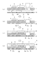
- FIG. 2 is a 1st process and shows the state which prepared the core board
- FIG. The core substrate 1 is a hard substrate, and an opening 2 and in-plane conductors 4 and 5 are formed.
- the second circuit component 6 is mounted on the in-plane conductor 4 on the upper surface in advance. However, the second circuit component 6 may be mounted after the core substrate 1 is bonded to the first resin layer 10.
- the first resin layer 10 is an uncured resin sheet, for example, an uncured sheet containing an inorganic filler and a thermosetting resin, an uncured sheet made of a thermosetting resin not containing an inorganic filler, A prepreg or the like can be used.
- interlayer connection conductors 11a and 11b are formed at positions corresponding to the terminal electrodes 3a of the first circuit component 3 and the in-plane conductors 5 of the core substrate 1, respectively. These interlayer connection conductors 11 a and 11 b are obtained by filling an interlayer connection conductor hole penetrating the first resin layer 10 with an uncured conductive paste. Further, the copper foil 12 is attached to the entire lower surface of the first resin layer 10 by the adhesive force of the first resin layer 10.
- FIG. 2B shows the second step, in which the core substrate 1 is pressure-bonded onto the first resin layer 10 and the first resin layer 10 in the opening 2 is exposed to the first circuit component 3. Crimp to the part. At this time, crimping is performed so that the in-plane conductor 5 of the core substrate 1 corresponds to the interlayer connection conductor 11b and the terminal electrode 3a of the first circuit component 3 corresponds to the interlayer connection conductor 11a. Since the uncured first resin layer 10 has adhesiveness, the core substrate 1 and the first circuit component 3 are temporarily fixed to the first resin layer 10. At this time, since the conductive paste constituting the interlayer connection conductor 11a is also uncured, the terminal electrode 3 of the first circuit component 3 and the interlayer connection conductor 11a are not electrically connected.
- FIG. 2C shows a third step, in which an uncured second resin layer 20 is laminated on the core substrate 1. Since the second resin layer 20 is uncured, the second resin layer 20 flows and fills the periphery of the second circuit component 6 without a gap, and the inner wall of the opening 2 and the first circuit component 3 is also filled in the gap. The first resin layer 10 and the second resin layer 20 are collectively cured by heating together with the lamination pressure bonding. As a result, the first resin layer 10 and the second resin layer 20 are integrated with the core substrate 1 in between.
- the interlayer connection conductors 11a and 11b are also cured at the same time to generate conductivity, so that the interlayer connection conductor 11a and the terminal electrode 3a of the first circuit component 3 are electrically connected, and the interlayer connection conductor 11b
- the in-plane conductor 5 of the core substrate 1 is electrically connected.
- FIG. 2D shows a fourth step, in which the copper foil 12 of the cured first resin layer 10 is patterned to form in-plane conductors 12a and 12b, thereby completing the component built-in module A.
- the pattern formation of the copper foil 12 can be formed by a known method such as etching.
- the in-plane conductors 12a and 12b are not only a method in which the copper foil 12 is attached to the uncured first resin layer 10 and etching is performed after the first resin layer 10 is cured, but also a plating method and a conductive paste printing method. It can also be formed by, for example.
- the first resin layer 10 and the second resin layer 20 are simultaneously cured, but the first resin layer 10 is first cured at the stage where the step (b) is completed. Also good. However, when the first resin layer 10 and the second resin layer 20 are made of the same material and are cured at the same time, the curing shrinkage of both the resin layers becomes the same, so that the generation of warp can be suppressed. There is.
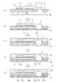
- FIG. 3 shows another example of the manufacturing method of the component built-in module A.
- (A) of FIG. 3 is a 1st process and shows the state which prepared the core board
- FIG. The core substrate 1 is the same as that in FIG. 2, but the first resin layer 10 is a thin resin sheet in which no interlayer connection conductor is formed. Copper foil is also not affixed.
- FIG. 3B shows the second step, in which the core substrate 1 is pressure-bonded onto the first resin layer 10 and the first resin layer 10 in the opening 2 is exposed to the first circuit component 3. Crimp to the part. Since the interlayer connection conductor is not yet formed on the first resin layer 10, it is not necessary to align the core substrate 1 and the first circuit component 3 with respect to the first resin layer 10, and the bonding operation is simple. become.
- FIG. 3C shows a third step, in which an uncured second resin layer 20 is laminated on the core substrate 1. Since the second resin layer 20 is uncured, the second resin layer 20 flows and fills the periphery of the second circuit component 6 without a gap, and the inner wall of the opening 2 and the first circuit component 3 is also filled in the gap. The first resin layer 10 and the second resin layer 20 are collectively cured by heating together with the lamination pressure bonding.
- FIG. 3D shows a fourth step, in which an interlayer connection conductor hole is formed at the position of the first resin layer 10 corresponding to the in-plane conductor 5 of the core substrate 1 and the terminal electrode 3 a of the first circuit component 3.
- 11a 1 and 11b 1 are formed by laser processing. By forming the interlayer connection conductor holes 11a 1 and 11b 1 , the in-plane conductor 5 and the terminal electrode 3a are exposed.
- FIG. 3E shows a fifth step, in which the interlayer connection conductors 11a and 11b are formed by filling and curing the interlayer connection conductor holes (via holes) 11a 1 and 11b 1 to form the interlayer connection conductors 11a and 11b.
- the in-plane conductors 12a and 12b that are electrically connected to the interlayer connection conductors 11a and 11b are formed in a pattern on the surface of the resin layer 10.
- Interlayer connection conductors 11a, 11b are filled conductive paste is not limited to curing, a conductive film is formed on the inner surface of the interlayer connection conductor holes 11a 1, 11b 1 by plating, holes 11a 1 for interlayer connection conductor , 11b 1 may be embedded with resin.
- As a method for forming the in-plane conductors 12a and 12b an arbitrary method such as plating or printing of a conductive paste can be selected.
- the interlayer connection conductor holes 11a 1 and 11b 1 after the first resin layer 10 is cured in order to form the interlayer connection conductor holes 11a 1 and 11b 1 after the first resin layer 10 is cured, and to form the interlayer connection conductors 11a and 11b by conductive paste or plating.
- the in-plane conductor 5 of the core substrate 1 and the terminal electrode 3a of the first circuit component 3 and the interlayer connection conductors 11a and 11b can be electrically and reliably connected.
- the first resin layer 10 and the second resin layer 20 are cured simultaneously, but the first resin layer 10 is cured before the second resin layer 20 is laminated. Also good. In that case, the interlayer connection conductors 11a and 11b may be formed before the second resin layer 20 is laminated.
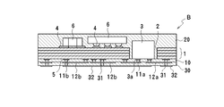
- FIG. 4 shows a second embodiment of the component built-in module.
- a further resin layer 30 is built up and laminated on the lower surface of the first resin layer 10 of the component built-in module A of the first embodiment.
- the resin layer 30 is a thin resin layer similar to the first resin layer 10, and the lower surface thereof includes in-plane conductors 12 a and 12 b of the first resin layer 10 via a plurality of interlayer connection conductors 31. A connected in-plane conductor 32 is formed.
- a resin layer may be further built up on the lower surface of the resin layer 30.
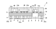
- FIG. 5 shows a third embodiment of the component built-in module.
- the third circuit component 40 is mounted on the in-plane conductors 12a and 12b on the back surface of the first resin layer 10 in order to increase the mounting density, and the first resin layer 10
- the third circuit component 40 is embedded in the third resin layer 50 by laminating the third resin layer 50 on the back surface of the substrate.
- the third circuit component 40 is preferably a lower-profile component than the first circuit component 3.
- the third resin layer 50 is preferably made of the same material as the first and second resin layers 10 and 20.
- a plurality of interlayer connection conductors 21 connected to the in-plane conductor pattern 4 of the core substrate 1 are formed on the second resin layer 20.
- the surface of the second resin layer 20 is connected to the interlayer connection conductor 21.
- An in-plane conductor pattern 22a is formed.
- FIG. 6 shows an example of the manufacturing process of the component built-in module C.
- (a) to (d) in FIG. 6 are substantially the same as (a) to (d) in FIG.
- the copper foil 22 is arranged on the surface of the second resin layer 20 at the stage of FIG. 6C, and the copper foil 22 is fixed to the surface of the second resin layer 20 at the time of pressure bonding / curing.
- FIG. 6 shows an example of the manufacturing process of the component built-in module C.
- the copper foil 22 is patterned to form an in-plane conductor pattern 22a, and an interlayer reaching the in-plane conductor 4 on the upper surface of the core substrate 1
- the interlayer connection conductor 21 is formed by laser processing the connection conductor hole (via hole) and filling the interlayer connection conductor hole with a conductive paste and curing. Further, the shape of a part of the second circuit component 6 is different from that in FIG.
- FIG. 6E the module obtained in FIG. 6D is turned upside down, and the third circuit component 40 is mounted on the in-plane conductors 12a and 12b on the back surface of the first resin layer 10.
- FIG. (f) of FIG. 6 an uncured third resin layer 50 is thermocompression-bonded on the first resin layer 10, and the periphery of the third circuit component 40 is covered with the third resin layer 50.
- the third resin layer 50 is cured to complete the component built-in module C.
- FIG. 6 a resin sheet in which the interlayer connection conductors 11a and 11b are formed in advance as the first resin layer 10 and the copper foil 12 is pasted on the entire lower surface is used. However, as shown in FIG. A resin sheet having no copper foil may be used, and the interlayer connection conductor may be formed after the resin sheet is cured.
- the hardening process of the 1st resin layer 10 and the 2nd resin layer 20 does not necessarily need to be simultaneous. That is, after temporarily fixing the core substrate 1 and the first circuit component 3 to the first resin layer 10, the first resin layer 10 is cured, and then the second resin layer 20 is laminated and cured. Also good. However, it is advantageous to simultaneously cure the first resin layer 10 and the second resin layer 20 in that the warpage of the module accompanying curing shrinkage can be reduced.
Landscapes
- Engineering & Computer Science (AREA)
- Microelectronics & Electronic Packaging (AREA)
- Manufacturing & Machinery (AREA)
- Production Of Multi-Layered Print Wiring Board (AREA)
Abstract
Description
本発明に係る部品内蔵モジュールの第1実施形態について、図1を参照しながら説明する。
ここで、前記部品内蔵モジュールAの製造方法の一例について、図2を参照しながら説明する。なお、図2では単一の部品内蔵モジュールAの製造方法について説明するが、実際の製造工程では親基板状態の部品内蔵モジュールが作製され、その後で子基板状態にカットされる。
図3は、前記部品内蔵モジュールAの製造方法の他の例を示す。図3の(a)は第1工程であり、コア基板1と未硬化の第1の樹脂層10とを準備した状態を示す。コア基板1は図2と同様であるが、第1の樹脂層10は層間接続導体が形成されていない薄層の樹脂シートである。銅箔も貼り付けられていない。
図4は部品内蔵モジュールの第2実施形態を示す。この実施形態の部品内蔵モジュールBでは、第1実施形態の部品内蔵モジュールAの第1の樹脂層10の下面に、さらなる樹脂層30をビルトアップ積層したものである。この樹脂層30は、第1の樹脂層10と同様に薄肉な樹脂層であり、その下面には、複数の層間接続導体31を介して第1の樹脂層10の面内導体12a,12bと接続された面内導体32が形成されている。なお、樹脂層30の下面にさらに樹脂層をビルトアップしてもよいことは勿論である。
図5は部品内蔵モジュールの第3実施形態を示す。この実施形態の部品内蔵モジュールCは、実装密度を高めるために、第1の樹脂層10の裏面の面内導体12a,12bに第3の回路部品40を実装すると共に、第1の樹脂層10の裏面に第3の樹脂層50を積層することで、第3の回路部品40を第3の樹脂層50の中に埋設したものである。第3の回路部品40は第1の回路部品3より低背部品がよい。第3の樹脂層50は第1,第2の樹脂層10,20と同質の材料とするのがよい。第2の樹脂層20には、コア基板1の面内導体パターン4と接続された複数の層間接続導体21が形成され、第2の樹脂層20の表面には、層間接続導体21と接続された面内導体パターン22aが形成されている。
1 コア基板
2 開口部
3 第1の回路部品
3a 端子電極
4,5 面内導体
6 第2回路部品
10 第1の樹脂層
11a,11b 電極(層間接続導体)
12a,12b 面内導体
20 第2の樹脂層
21 層間接続導体
30 ビルドアップ樹脂層
40 第3の回路部品
50 第3の樹脂層
Claims (12)
- 表裏方向に貫通した開口部を有するコア基板を未硬化状態の第1の樹脂層上に積層する工程Aと、
前記開口部内に露出した未硬化状態の前記第1の樹脂層の露出部分に第1の回路部品を付着させる工程Bと、
前記コア基板上に未硬化状態の第2の樹脂層を積層し、前記開口部の内壁と前記第1の回路部品との隙間に第2の樹脂層を充填する工程Cと、
前記第1の樹脂層を硬化させる工程Dと、
前記第2の樹脂層を硬化させる工程Eと、を備えることを特徴とする部品内蔵モジュールの製造方法。 - 前記工程Bの前の前記第1の樹脂層に、当該第1の樹脂層を貫通する層間接続導体用穴と当該層間接続導体用穴に充填された未硬化の導電ペーストとからなる電極が形成され、
前記工程Bにおいて、前記第1の回路部品を前記電極と接するように前記第1の樹脂層に付着させ、
前記工程Dにおいて、前記第1の樹脂層を硬化させると同時に前記導電ペーストを硬化させて前記第1の回路部品と前記電極とを電気的に接続することを特徴とする請求項1に記載の部品内蔵モジュールの製造方法。 - 前記工程Dの後、前記第1の樹脂層に前記第1の回路部品に達するように層間接続導体用穴を形成し、当該層間接続導体用穴の中に層間接続導体を形成することにより、前記第1の回路部品と電気的に接続された電極を形成することを特徴とする請求項1に記載の部品内蔵モジュールの製造方法。
- 前記工程Dと工程Eとを同時に実施することを特徴とする請求項1乃至3のいずれか1項に記載の部品内蔵モジュールの製造方法。
- 前記第1の回路部品は前記コア基板の厚みよりも高背な部品であることを特徴とする請求項1乃至4のいずれか1項に記載の部品内蔵モジュールの製造方法。
- 前記工程Cの前に、前記コア基板上に前記第1の回路部品より低背な第2の回路部品を実装する工程を備え、
前記工程Cにおいて、前記第2の回路部品を前記第2の樹脂層中に埋設することを特徴とする請求項1乃至5のいずれか1項に記載の部品内蔵モジュールの製造方法。 - 前記第1の樹脂層と前記第2の樹脂層とは同一材質よりなることを特徴とする請求項1乃至6のいずれか1項に記載の部品内蔵モジュールの製造方法。
- 第1の樹脂層と、
前記第1の樹脂層上に積層され、表裏方向に貫通した開口部を有するコア基板と、
前記コア基板の開口部内に収納され、底面が前記第1の樹脂層上に付着された第1の回路部品と、
前記コア基板上に積層され、前記コア基板の開口部と前記第1の回路部品との隙間に充填された第2の樹脂層と、
前記第1の樹脂層に形成されるとともに、前記第1の回路部品と電気的に接続された電極と、を備えたことを特徴とする部品内蔵モジュール。 - 前記電極は、前記第1の回路部品に達するように前記第1の樹脂層に形成された層間接続導体であることを特徴とする請求項8に記載の部品内蔵モジュール。
- 前記第1の回路部品は前記コア基板の厚みよりも高背な部品であることを特徴とする請求項8又は9に記載の部品内蔵モジュール。
- 前記コア基板上に実装され、かつ前記第2の樹脂層中に埋設された、前記第1の回路部品より低背な第2の回路部品をさらに備えることを特徴とする請求項8乃至10のいずれか1項に記載の部品内蔵モジュール。
- 前記第1の樹脂層と前記第2の樹脂層とは同一材質よりなることを特徴とする請求項8乃至11のいずれか1項に記載の部品内蔵モジュール。
Priority Applications (2)
| Application Number | Priority Date | Filing Date | Title |
|---|---|---|---|
| CN200980131635.2A CN102119588B (zh) | 2008-08-12 | 2009-06-09 | 元器件内置模块的制造方法及元器件内置模块 |
| JP2010524681A JP5093353B2 (ja) | 2008-08-12 | 2009-06-09 | 部品内蔵モジュールの製造方法及び部品内蔵モジュール |
Applications Claiming Priority (2)
| Application Number | Priority Date | Filing Date | Title |
|---|---|---|---|
| JP2008207831 | 2008-08-12 | ||
| JP2008-207831 | 2008-08-12 |
Publications (1)
| Publication Number | Publication Date |
|---|---|
| WO2010018708A1 true WO2010018708A1 (ja) | 2010-02-18 |
Family
ID=41668855
Family Applications (1)
| Application Number | Title | Priority Date | Filing Date |
|---|---|---|---|
| PCT/JP2009/060496 Ceased WO2010018708A1 (ja) | 2008-08-12 | 2009-06-09 | 部品内蔵モジュールの製造方法及び部品内蔵モジュール |
Country Status (3)
| Country | Link |
|---|---|
| JP (1) | JP5093353B2 (ja) |
| CN (2) | CN102119588B (ja) |
| WO (1) | WO2010018708A1 (ja) |
Cited By (11)
| Publication number | Priority date | Publication date | Assignee | Title |
|---|---|---|---|---|
| JP2011187831A (ja) * | 2010-03-10 | 2011-09-22 | Tdk Corp | 電子部品内蔵基板及びその製造方法 |
| CN102907187A (zh) * | 2010-05-26 | 2013-01-30 | 株式会社村田制作所 | 元器件内置基板 |
| JP2013093456A (ja) * | 2011-10-26 | 2013-05-16 | Nippon Dempa Kogyo Co Ltd | 電子モジュールとその製造方法 |
| WO2014017228A1 (ja) * | 2012-07-26 | 2014-01-30 | 株式会社村田製作所 | モジュール |
| JP2014049558A (ja) * | 2012-08-30 | 2014-03-17 | Shinko Electric Ind Co Ltd | 配線基板、及び、配線基板の製造方法 |
| JP2015002295A (ja) * | 2013-06-17 | 2015-01-05 | 味の素株式会社 | 部品内蔵回路板の製造方法、および半導体装置 |
| US9425122B2 (en) | 2012-12-21 | 2016-08-23 | Panasonic Intellectual Property Management Co., Ltd. | Electronic component package and method for manufacturing the same |
| US9449944B2 (en) | 2012-12-21 | 2016-09-20 | Panasonic Intellectual Property Management Co., Ltd. | Electronic component package and method for manufacturing same |
| US9595651B2 (en) | 2012-12-21 | 2017-03-14 | Panasonic Intellectual Property Management Co., Ltd. | Electronic component package and method for manufacturing same |
| TWI586232B (zh) * | 2012-03-07 | 2017-06-01 | Lg伊諾特股份有限公司 | 印刷電路板及其製造方法 |
| US9825209B2 (en) | 2012-12-21 | 2017-11-21 | Panasonic Intellectual Property Management Co., Ltd. | Electronic component package and method for manufacturing the same |
Families Citing this family (2)
| Publication number | Priority date | Publication date | Assignee | Title |
|---|---|---|---|---|
| CN105922938B (zh) * | 2016-04-26 | 2020-09-25 | 北京兴科迪科技有限公司 | 一种轻量化防眩目后视镜及其制作方法 |
| CN118215204A (zh) * | 2024-03-21 | 2024-06-18 | 中国电子科技集团公司第二十六研究所 | 一种压合埋置式pcb封装结构及其制备方法 |
Citations (5)
| Publication number | Priority date | Publication date | Assignee | Title |
|---|---|---|---|---|
| JP2000332057A (ja) * | 1999-05-18 | 2000-11-30 | Ngk Spark Plug Co Ltd | 配線基板及び電子部品を搭載した配線基板の製造方法 |
| WO2005101934A1 (ja) * | 2004-04-06 | 2005-10-27 | Murata Manufacturing Co., Ltd. | 複合型電子部品及びその製造方法 |
| JP2007012761A (ja) * | 2005-06-29 | 2007-01-18 | Tdk Corp | 半導体ic内蔵基板及びその製造方法 |
| JP2008091377A (ja) * | 2006-09-29 | 2008-04-17 | Toppan Printing Co Ltd | プリント配線基板及びその製造方法 |
| JP2009081423A (ja) * | 2007-09-05 | 2009-04-16 | Taiyo Yuden Co Ltd | 電子部品内蔵型多層基板およびその製造方法 |
Family Cites Families (6)
| Publication number | Priority date | Publication date | Assignee | Title |
|---|---|---|---|---|
| KR100488412B1 (ko) * | 2001-06-13 | 2005-05-11 | 가부시키가이샤 덴소 | 내장된 전기소자를 갖는 인쇄 배선 기판 및 그 제조 방법 |
| TW550997B (en) * | 2001-10-18 | 2003-09-01 | Matsushita Electric Industrial Co Ltd | Module with built-in components and the manufacturing method thereof |
| US7394663B2 (en) * | 2003-02-18 | 2008-07-01 | Matsushita Electric Industrial Co., Ltd. | Electronic component built-in module and method of manufacturing the same |
| JP2006128229A (ja) * | 2004-10-26 | 2006-05-18 | Murata Mfg Co Ltd | 複合多層基板 |
| JP4945974B2 (ja) * | 2005-09-09 | 2012-06-06 | 大日本印刷株式会社 | 部品内蔵配線板 |
| KR100788213B1 (ko) * | 2006-11-21 | 2007-12-26 | 삼성전기주식회사 | 전자소자 내장형 인쇄회로기판의 제조방법 |
-
2009
- 2009-06-09 WO PCT/JP2009/060496 patent/WO2010018708A1/ja not_active Ceased
- 2009-06-09 CN CN200980131635.2A patent/CN102119588B/zh not_active Expired - Fee Related
- 2009-06-09 JP JP2010524681A patent/JP5093353B2/ja not_active Expired - Fee Related
- 2009-06-09 CN CN201410043635.XA patent/CN103747616B/zh active Active
Patent Citations (5)
| Publication number | Priority date | Publication date | Assignee | Title |
|---|---|---|---|---|
| JP2000332057A (ja) * | 1999-05-18 | 2000-11-30 | Ngk Spark Plug Co Ltd | 配線基板及び電子部品を搭載した配線基板の製造方法 |
| WO2005101934A1 (ja) * | 2004-04-06 | 2005-10-27 | Murata Manufacturing Co., Ltd. | 複合型電子部品及びその製造方法 |
| JP2007012761A (ja) * | 2005-06-29 | 2007-01-18 | Tdk Corp | 半導体ic内蔵基板及びその製造方法 |
| JP2008091377A (ja) * | 2006-09-29 | 2008-04-17 | Toppan Printing Co Ltd | プリント配線基板及びその製造方法 |
| JP2009081423A (ja) * | 2007-09-05 | 2009-04-16 | Taiyo Yuden Co Ltd | 電子部品内蔵型多層基板およびその製造方法 |
Cited By (12)
| Publication number | Priority date | Publication date | Assignee | Title |
|---|---|---|---|---|
| JP2011187831A (ja) * | 2010-03-10 | 2011-09-22 | Tdk Corp | 電子部品内蔵基板及びその製造方法 |
| CN102907187A (zh) * | 2010-05-26 | 2013-01-30 | 株式会社村田制作所 | 元器件内置基板 |
| JP2013093456A (ja) * | 2011-10-26 | 2013-05-16 | Nippon Dempa Kogyo Co Ltd | 電子モジュールとその製造方法 |
| TWI586232B (zh) * | 2012-03-07 | 2017-06-01 | Lg伊諾特股份有限公司 | 印刷電路板及其製造方法 |
| WO2014017228A1 (ja) * | 2012-07-26 | 2014-01-30 | 株式会社村田製作所 | モジュール |
| US9293446B2 (en) | 2012-07-26 | 2016-03-22 | Murata Manufacturing Co., Ltd. | Low profile semiconductor module with metal film support |
| JP2014049558A (ja) * | 2012-08-30 | 2014-03-17 | Shinko Electric Ind Co Ltd | 配線基板、及び、配線基板の製造方法 |
| US9425122B2 (en) | 2012-12-21 | 2016-08-23 | Panasonic Intellectual Property Management Co., Ltd. | Electronic component package and method for manufacturing the same |
| US9449944B2 (en) | 2012-12-21 | 2016-09-20 | Panasonic Intellectual Property Management Co., Ltd. | Electronic component package and method for manufacturing same |
| US9595651B2 (en) | 2012-12-21 | 2017-03-14 | Panasonic Intellectual Property Management Co., Ltd. | Electronic component package and method for manufacturing same |
| US9825209B2 (en) | 2012-12-21 | 2017-11-21 | Panasonic Intellectual Property Management Co., Ltd. | Electronic component package and method for manufacturing the same |
| JP2015002295A (ja) * | 2013-06-17 | 2015-01-05 | 味の素株式会社 | 部品内蔵回路板の製造方法、および半導体装置 |
Also Published As
| Publication number | Publication date |
|---|---|
| CN102119588B (zh) | 2014-03-05 |
| JP5093353B2 (ja) | 2012-12-12 |
| CN103747616B (zh) | 2018-03-30 |
| JPWO2010018708A1 (ja) | 2012-01-26 |
| CN102119588A (zh) | 2011-07-06 |
| CN103747616A (zh) | 2014-04-23 |
Similar Documents
| Publication | Publication Date | Title |
|---|---|---|
| JP5093353B2 (ja) | 部品内蔵モジュールの製造方法及び部品内蔵モジュール | |
| US8178191B2 (en) | Multilayer wiring board and method of making the same | |
| US8177577B2 (en) | Printed wiring board having a substrate with higher conductor density inserted into a recess of another substrate with lower conductor density | |
| JP6281016B2 (ja) | 回路基板及びその製造方法 | |
| WO2010007704A1 (ja) | フレックスリジッド配線板及び電子デバイス | |
| TWI405511B (zh) | 具有電子部件的印刷電路板以及其製造方法 | |
| CN107068576A (zh) | 制造柔性电子器件的方法 | |
| CN107295747A (zh) | 器件载体及制造器件载体的方法 | |
| JP2001332866A (ja) | 回路基板及びその製造方法 | |
| CN107295746A (zh) | 器件载体及其制造方法 | |
| JP2016134624A (ja) | 電子素子内蔵型印刷回路基板及びその製造方法 | |
| WO2010103695A1 (ja) | 部品内蔵モジュールの製造方法及び部品内蔵モジュール | |
| WO2011148915A1 (ja) | モジュール基板およびその製造方法 | |
| JP5462450B2 (ja) | 部品内蔵プリント配線板及び部品内蔵プリント配線板の製造方法 | |
| JP3733419B2 (ja) | 電子部品内蔵型多層基板とその製造方法及びそれに使用するメタルコア基板 | |
| CN104247582B (zh) | 印刷电路板及其制造方法 | |
| US12520423B2 (en) | Method for manufacturing circuit board | |
| KR20160103270A (ko) | 인쇄회로기판 및 그 제조방법 | |
| JP2005268378A (ja) | 部品内蔵基板の製造方法 | |
| JP5749235B2 (ja) | 回路部品内蔵基板の製造方法 | |
| JP5221682B2 (ja) | プリント回路基板及びその製造方法 | |
| JP2009289789A (ja) | 部品内蔵プリント配線板及び部品内蔵プリント配線板の製造方法 | |
| JP4899409B2 (ja) | 多層プリント配線基板及びその製造方法 | |
| JP2007115952A (ja) | インターポーザ基板及びその製造方法 | |
| JP4529594B2 (ja) | 配線基板の製造方法 |
Legal Events
| Date | Code | Title | Description |
|---|---|---|---|
| WWE | Wipo information: entry into national phase |
Ref document number: 200980131635.2 Country of ref document: CN |
|
| 121 | Ep: the epo has been informed by wipo that ep was designated in this application |
Ref document number: 09806604 Country of ref document: EP Kind code of ref document: A1 |
|
| WWE | Wipo information: entry into national phase |
Ref document number: 2010524681 Country of ref document: JP |
|
| NENP | Non-entry into the national phase |
Ref country code: DE |
|
| 122 | Ep: pct application non-entry in european phase |
Ref document number: 09806604 Country of ref document: EP Kind code of ref document: A1 |