WO2010013636A1 - 配線膜、薄膜トランジスタ、ターゲット、配線膜の形成方法 - Google Patents
配線膜、薄膜トランジスタ、ターゲット、配線膜の形成方法 Download PDFInfo
- Publication number
- WO2010013636A1 WO2010013636A1 PCT/JP2009/063185 JP2009063185W WO2010013636A1 WO 2010013636 A1 WO2010013636 A1 WO 2010013636A1 JP 2009063185 W JP2009063185 W JP 2009063185W WO 2010013636 A1 WO2010013636 A1 WO 2010013636A1
- Authority
- WO
- WIPO (PCT)
- Prior art keywords
- film
- atomic
- layer
- barrier film
- low resistance
- Prior art date
- Legal status (The legal status is an assumption and is not a legal conclusion. Google has not performed a legal analysis and makes no representation as to the accuracy of the status listed.)
- Ceased
Links
Images




Classifications
-
- H—ELECTRICITY
- H10—SEMICONDUCTOR DEVICES; ELECTRIC SOLID-STATE DEVICES NOT OTHERWISE PROVIDED FOR
- H10D—INORGANIC ELECTRIC SEMICONDUCTOR DEVICES
- H10D30/00—Field-effect transistors [FET]
- H10D30/60—Insulated-gate field-effect transistors [IGFET]
- H10D30/67—Thin-film transistors [TFT]
- H10D30/6729—Thin-film transistors [TFT] characterised by the electrodes
- H10D30/6737—Thin-film transistors [TFT] characterised by the electrodes characterised by the electrode materials
- H10D30/6739—Conductor-insulator-semiconductor electrodes
-
- C—CHEMISTRY; METALLURGY
- C22—METALLURGY; FERROUS OR NON-FERROUS ALLOYS; TREATMENT OF ALLOYS OR NON-FERROUS METALS
- C22C—ALLOYS
- C22C19/00—Alloys based on nickel or cobalt
- C22C19/03—Alloys based on nickel or cobalt based on nickel
- C22C19/05—Alloys based on nickel or cobalt based on nickel with chromium
-
- C—CHEMISTRY; METALLURGY
- C23—COATING METALLIC MATERIAL; COATING MATERIAL WITH METALLIC MATERIAL; CHEMICAL SURFACE TREATMENT; DIFFUSION TREATMENT OF METALLIC MATERIAL; COATING BY VACUUM EVAPORATION, BY SPUTTERING, BY ION IMPLANTATION OR BY CHEMICAL VAPOUR DEPOSITION, IN GENERAL; INHIBITING CORROSION OF METALLIC MATERIAL OR INCRUSTATION IN GENERAL
- C23C—COATING METALLIC MATERIAL; COATING MATERIAL WITH METALLIC MATERIAL; SURFACE TREATMENT OF METALLIC MATERIAL BY DIFFUSION INTO THE SURFACE, BY CHEMICAL CONVERSION OR SUBSTITUTION; COATING BY VACUUM EVAPORATION, BY SPUTTERING, BY ION IMPLANTATION OR BY CHEMICAL VAPOUR DEPOSITION, IN GENERAL
- C23C14/00—Coating by vacuum evaporation, by sputtering or by ion implantation of the coating forming material
- C23C14/06—Coating by vacuum evaporation, by sputtering or by ion implantation of the coating forming material characterised by the coating material
- C23C14/14—Metallic material, boron or silicon
- C23C14/18—Metallic material, boron or silicon on other inorganic substrates
- C23C14/185—Metallic material, boron or silicon on other inorganic substrates by cathodic sputtering
-
- H—ELECTRICITY
- H10—SEMICONDUCTOR DEVICES; ELECTRIC SOLID-STATE DEVICES NOT OTHERWISE PROVIDED FOR
- H10D—INORGANIC ELECTRIC SEMICONDUCTOR DEVICES
- H10D30/00—Field-effect transistors [FET]
- H10D30/60—Insulated-gate field-effect transistors [IGFET]
- H10D30/67—Thin-film transistors [TFT]
- H10D30/6729—Thin-film transistors [TFT] characterised by the electrodes
- H10D30/6737—Thin-film transistors [TFT] characterised by the electrodes characterised by the electrode materials
-
- H—ELECTRICITY
- H10—SEMICONDUCTOR DEVICES; ELECTRIC SOLID-STATE DEVICES NOT OTHERWISE PROVIDED FOR
- H10D—INORGANIC ELECTRIC SEMICONDUCTOR DEVICES
- H10D30/00—Field-effect transistors [FET]
- H10D30/60—Insulated-gate field-effect transistors [IGFET]
- H10D30/67—Thin-film transistors [TFT]
- H10D30/674—Thin-film transistors [TFT] characterised by the active materials
- H10D30/6741—Group IV materials, e.g. germanium or silicon carbide
- H10D30/6743—Silicon
-
- H—ELECTRICITY
- H10—SEMICONDUCTOR DEVICES; ELECTRIC SOLID-STATE DEVICES NOT OTHERWISE PROVIDED FOR
- H10D—INORGANIC ELECTRIC SEMICONDUCTOR DEVICES
- H10D86/00—Integrated devices formed in or on insulating or conducting substrates, e.g. formed in silicon-on-insulator [SOI] substrates or on stainless steel or glass substrates
- H10D86/40—Integrated devices formed in or on insulating or conducting substrates, e.g. formed in silicon-on-insulator [SOI] substrates or on stainless steel or glass substrates characterised by multiple TFTs
- H10D86/441—Interconnections, e.g. scanning lines
-
- H—ELECTRICITY
- H10—SEMICONDUCTOR DEVICES; ELECTRIC SOLID-STATE DEVICES NOT OTHERWISE PROVIDED FOR
- H10D—INORGANIC ELECTRIC SEMICONDUCTOR DEVICES
- H10D86/00—Integrated devices formed in or on insulating or conducting substrates, e.g. formed in silicon-on-insulator [SOI] substrates or on stainless steel or glass substrates
- H10D86/40—Integrated devices formed in or on insulating or conducting substrates, e.g. formed in silicon-on-insulator [SOI] substrates or on stainless steel or glass substrates characterised by multiple TFTs
- H10D86/60—Integrated devices formed in or on insulating or conducting substrates, e.g. formed in silicon-on-insulator [SOI] substrates or on stainless steel or glass substrates characterised by multiple TFTs wherein the TFTs are in active matrices
Definitions
- the present invention relates to a metal wiring film for electronic parts and a transistor using the metal wiring film.
- low resistance materials such as Al and Cu, Mo, Cr, and the like are used for metal wiring films for electronic components.
- TFT Thin Film Transistor
- the demand for lower resistance of wiring electrodes is increasing as the panel size increases, and the need to use Al or Cu as low resistance wiring is increasing.
- Cu is a material having a lower resistance than Al.
- Al has a problem of deterioration of contact resistance with the ITO transparent electrode, but Cu has a good contact resistance because it is difficult to oxidize.
- Cu has problems such as poor adhesion to a base material such as glass or Si as compared with other wiring materials, and Cu diffuses into the Si layer when used as a source or drain electrode.
- a barrier layer for improving adhesion and preventing diffusion is required at the interface between the Cu wiring and other layers.
- the present invention has been made to solve the above-mentioned problems, and an object of the present invention is to provide a barrier film having high diffusion preventing ability and high adhesion.
- the present invention provides a wiring film that contacts at least one film formation target layer selected from the group consisting of a glass substrate, a silicon layer, and an oxide semiconductor layer,
- the film includes a barrier film disposed in close contact with the surface of the film formation target layer, and a metal low resistance layer disposed in close contact with the surface of the barrier film.
- the metal low resistance layer includes 50 atomic% of Cu.
- the barrier film contains Ni of 50 atomic% or more and an additive element of 7 atomic% or more and 50 atomic% or less, and the additive elements include V, Al, Mo, Ti,
- the wiring film is selected from an additive element group consisting of Zr, Cr, Si, W, Ta, In, Sn, Zn, Mn, and Cu.
- the present invention includes a gate electrode, a semiconductor layer disposed on the gate electrode, a gate insulating film disposed between the gate electrode and the semiconductor layer, and a connection electrode electrically connected to the semiconductor layer
- the connection electrode includes a barrier film disposed in close contact with the semiconductor layer, and a metal low resistance layer disposed in close contact with a surface of the barrier film opposite to the semiconductor layer.
- the metal low-resistance layer contains 50 atomic% or more of Cu
- the barrier film has 50 atomic% or more of Ni and 7 atomic% or more and 50 atomic% or less of an additive element, , V, Al, Mo, Ti, Zr, Cr, Si, W, Ta, In, Sn, Zn, Mn, and Cu. It is a thin film transistor.
- the present invention is a thin film transistor having a gate electrode disposed on a glass substrate, a semiconductor layer disposed on the gate electrode, and a gate insulating film disposed between the semiconductor layer and the gate electrode.
- the gate electrode includes a barrier film disposed in close contact with the surface of the glass substrate, and a metal low resistance layer disposed in close contact with the surface of the barrier film opposite to the glass substrate, and the metal low resistance layer Contains 50 atomic% or more of Cu, the barrier film has 50 atomic% or more of Ni and 7 atomic% or more and 50 atomic% or less of additive elements, and the additive elements include V, Al,
- the thin film transistor is selected from an additive element group consisting of Mo, Ti, Zr, Cr, Si, W, Ta, In, Sn, Zn, Mn, and Cu.
- the present invention is a target that contains 50 atomic% or more of Ni, V, Al, Mo, Ti, Zr, Cr, Si, W, Ta, In, Sn, It is a target to which any one or more kinds of additive elements selected from the additive element group consisting of Zn, Mn, and Cu are added.
- the present invention relates to a wiring film forming method for forming a wiring film on a surface of at least one film formation target layer selected from the group consisting of a glass substrate, a silicon layer, and an oxide semiconductor layer, comprising 50 atoms.
- % Of Ni and 7 atomic% or more and 50 atomic% or less of an additive element, and the additive elements are V, Al, Mo, Ti, Zr, Cr, Si, W, and the like.
- the present invention is a method of forming a wiring film, wherein after the barrier film and the metal low resistance layer are formed, the barrier film and the metal low resistance layer are patterned with the same etchant. .
- the wiring film of the present invention is a film that adheres to a semiconductor layer (silicon layer, oxide semiconductor layer), a transparent conductive film, or a glass substrate, specifically, a TFT source electrode, drain electrode, gate electrode, storage capacitor electrode, etc. It is particularly suitable for these electrodes. It can also be used for barrier films and electrodes (wiring films) of other electronic components such as semiconductor elements and wiring boards.
- the silicon layer includes a silicon layer doped with impurities (ohmic contact layer) in addition to a silicon-based material such as polysilicon or amorphous silicon.
- the barrier film contains 50 atomic% or more of Ni, the adhesion to the glass substrate, the silicon layer, and the oxide semiconductor layer is higher than that of the metal low resistance layer. Since the adhesion between the barrier film and the metal low resistance layer is also high, the wiring film is difficult to peel off from the film formation target. The electrical resistance of the wiring film is lowered by laminating the metal low resistance layer on the barrier film. Since the barrier film and the metal low resistance layer can be etched with the same etchant, it is not necessary to separate the etching process, and the manufacturing time and manufacturing cost of the wiring film and the thin film transistor can be shortened.
- Sectional drawing explaining an example of the film-forming apparatus used for this invention Sectional drawing explaining the process of forming a laminated film Sectional drawing explaining the process of forming a laminated film Sectional drawing explaining the process of forming a laminated film Sectional drawing explaining the manufacturing process of the thin-film transistor of a 1st example Sectional drawing explaining the manufacturing process of the thin-film transistor of a 1st example Sectional drawing explaining the manufacturing process of the thin-film transistor of a 1st example Sectional drawing explaining the manufacturing process of the thin-film transistor of a 1st example Sectional drawing explaining an example of a liquid crystal display device Sectional drawing explaining the thin-film transistor of a 2nd example Sectional drawing explaining the thin-film transistor of a 3rd example
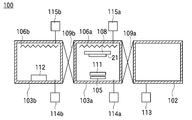
- Reference numeral 100 in FIG. 1 shows an example of a film forming apparatus used in the present invention.
- the film forming apparatus 100 includes a carry-in / out chamber 102, a first film forming chamber 103a, and a second film forming chamber 103b.
- the carry-in / out chamber 102 and the first film forming chamber 103a and the first film forming chamber 103a and the second film forming chamber 103b are connected to each other through gate valves 109a and 109b, respectively.
- the evacuation systems 113, 114a, 114b are connected to the carry-in / out chamber 102 and the first and second film forming chambers 103a, 103b, respectively, and the gate valves 109a, 109b are closed, and the first and second components are formed.
- the inside of the film chambers 103a and 103b is evacuated.
- the door between the loading / unloading chamber 102 and the atmosphere is opened, the film formation target 21 is loaded into the loading / unloading chamber 102, the door is closed, the inside of the loading / unloading chamber 102 is evacuated, the gate valve 109 a is opened, The film formation target 21 is moved into the first film formation chamber 103 a and is held by the substrate holder 108.
- a nickel target 111 of the present invention and a copper target (here, pure copper target made of copper) 112 are disposed on the bottom wall side inside the first and second film forming chambers 103a and 103b, respectively.
- the object 21 is held by the substrate holder 108 so as to face each of the targets 111 and 112.
- Gas introduction systems 115a and 115b are connected to the first and second film formation chambers 103a and 103b, respectively, and a sputtering gas is introduced from the gas introduction system 115a while evacuating the inside of the first film formation chamber 103a. Then, a voltage is applied to the nickel target 111 from a power source (not shown) to perform sputtering.
- a magnet 105 (permanent magnet or electromagnet) is disposed on the surface (back surface) opposite to the substrate holder 108 of the nickel target 111. Magnetic field lines passing through the surface of the nickel target 111 are formed by the magnet 105, the plasma density on the surface of the nickel target 111 is increased, and the sputtering speed is increased compared to the case without the magnet 105 (magnetron sputtering).
- the nickel target 111 of the present invention has a Ni content of 50% or more, and V, Al, Mo, Ti, Zr, Cr, Si, W, Ta, In, and Sn. And an alloy target to which any one or more kinds of nonmagnetic materials selected from the group consisting of Zn, Mn, and Cu are added as additive elements.
- the target is composed only of a magnetic material such as Ni, it is difficult to generate a magnetic field suitable for film formation by magnetron sputtering, but the nickel target 111 of the present invention is non-added by adding an additive element. Since it is magnetized, the sputtering speed is faster than when magnetron sputtering is performed and the magnet 105 is not disposed.
- nickel particles and additive element particles are released as sputtered particles. That is, nickel atoms and additive elements are released from the nickel target 111.
- any one or more of a glass layer (glass substrate and the like), a silicon layer, and an oxide semiconductor layer are exposed on the surface (film formation surface) 19 of the film formation target 21.
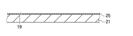
- the film formation target 21 is held by the substrate holder 108 with the film formation surface 19 facing the nickel target 111, the sputtered particles emitted from the nickel target 111 are incident on the film formation surface 19, and the barrier film 25 is formed on the film formation surface 19. (FIG. 2A).
- the atomic composition of the barrier film 25 is substantially equal to the atomic composition of the nickel target 111.
- the barrier film 25 has a Ni content of 50 atomic% or more, and V, Al, Mo, Ti, Zr, Cr, Si, W, Ta, In, Sn, and V.
- One or more types of nonmagnetic materials selected from the group consisting of Zn, Mn, and Cu are added as additive elements.
- Sputtering may be performed by supplying a reaction gas (for example, an oxidizing gas such as O 2 ) from the reaction gas supply system to the first film formation chamber 103a, and in this case, the barrier film 25 includes nickel and an additive element. In addition, it contains constituent atoms of the reaction gas.
- a reaction gas for example, an oxidizing gas such as O 2
- the barrier film 25 includes nickel and an additive element. In addition, it contains constituent atoms of the reaction gas.
- the substrate holder 108 holding the film formation target 21 is moved to the second film formation chamber 103b. While evacuating the second film formation chamber 103b, a sputtering gas is introduced from the gas introduction system 115b, and a copper target (here, a pure copper target) 112 containing 50 atomic% or more of Cu is sputtered.
- a sputtering gas is introduced from the gas introduction system 115b, and a copper target (here, a pure copper target) 112 containing 50 atomic% or more of Cu is sputtered.
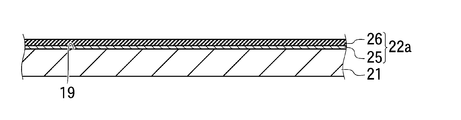
- the barrier film 25 and the metal A laminated film 22a of the low resistance layer 26 is formed (FIG. 2B).
- the metal low resistance layer 26 is formed by sputtering a copper target to which another additive metal such as nickel is added at 50 atomic% or less. May be. In any case, the metal low resistance layer 26 has a higher copper content than the barrier film 25, and the electric resistance of the metal low resistance layer 26 is lower than the electric resistance of the barrier film 25.
- the pure copper target 112 may be sputtered while supplying a reactive gas such as an oxidizing gas to the second film forming chamber 103b.
- the laminated film 22a may be composed of only the barrier film 25. However, when the barrier film 25 is a thin film and the thick metal low resistance layer 26 is laminated rather than the barrier film 25, the overall electric resistance is lowered.
- the laminated film 22 b may be configured by the resistance layer 26 and the barrier films 25 and 28 formed on the surface of the metal low resistance layer 26.
- the film formation target 21 on which the laminated films 22 a and 22 b are formed is unloaded from the film formation apparatus 100.
- a resist patterned in a predetermined shape is disposed on the laminated films 22a and 22b, and the laminated films 22a and 22b are etched with an etchant.
- Nickel can be etched with the same etchant as copper (for example, an etchant containing nitric acid), and the difference between the nickel etching rate and the copper etching rate is small. Therefore, the metal low resistance layer 26 and the barrier films 25 and 28 can be continuously etched with the same etchant. Therefore, the laminated films 22a and 22b are patterned into a predetermined shape in one etching process, and an electrode is formed.
- the barrier film 25 is located on the contact surface of the electrode that contacts the film formation target 21.
- the barrier film 25 contains 50 atomic% or more of nickel, and adheres to a glass layer (glass substrate), a silicon layer (silicon semiconductor layer, ohmic contact layer), and an oxide semiconductor layer (ZnO, In—Ga—Zn—O). Is expensive.
- the electrode is the surface of the film formation target 21. Hard to peel off.
- the barrier film 25 containing 50 atomic% or more of nickel has a function of preventing copper atoms from diffusing from the metal low-resistance layer 26 to the semiconductor layer, so that a silicon semiconductor layer, When a semiconductor layer such as an oxide semiconductor layer is exposed, copper is prevented from diffusing into the semiconductor layer.
- Nickel and an additive metal V were blended to form a nickel target 111, and the nickel target 111 was examined for magnetism and non-magnetism. The results are shown in Table 1 below together with the amount of V.
- the nickel target 111 is magnetron sputtered in the first film formation chamber 103a of FIG. 1 to form a barrier film 25 having a film thickness of 50 nm on the surface of the film formation target 21, and then a pure copper target 112 is sputtered to form a barrier.
- a laminated film 22a in which a 300 nm-thick metal low resistance layer 26 was laminated on the surface of the film 25 was formed, and a test piece having a structure shown in FIG. 2B was obtained.
- the barrier film 25 and the metal low resistance layer 26 were formed while introducing only the sputtering gas (Ar gas) into the first and second film formation chambers 103a and 103b and heating the film formation target 21 to 100 ° C. .
- Ar gas sputtering gas
- the laminated film 22a of each test piece was etched with an etching solution (mixed solution of sulfuric acid, nitric acid and acetic acid), and the etching characteristics were examined.
- etching solution mixed solution of sulfuric acid, nitric acid and acetic acid
- a case where the difference in etching rate between the barrier film 25 and the metal low resistance layer 26 is small and etching is possible with the same etching solution is “ ⁇ ”, and a case where the etching rate is large and etching is not possible with the same etching solution. It was described in Table 1 as “ ⁇ ”.
- the nickel target 111 was produced by changing the kind of the additive element, the laminated film 22a was formed using the nickel target 111, and a test piece was produced.
- the formation conditions of the laminated film 22a other than the type of additive element were the same as described above.
- the above “etching characteristics” and the following “adhesion” and “barrier properties” were examined.
- a laminated film 22a was formed on the surface of the glass substrate to obtain a test piece.
- On the surface on which the laminated film 22a of the test piece is formed put a 1mm square mass in 10 rows x 10 columns, a total of 100 notches, with a sharp knife at the tip, and stick adhesive tape (Scotch tape of model number 610) After the application, the number of films remaining when the adhesive tape was peeled off was evaluated. 0/100 when completely peeled, 100/100 when none peeled, and 90/100 or more is practically sufficient.
- a laminated film 22a was formed on the surface of an amorphous silicon silicon substrate to obtain a test piece. After the laminated film 22a was removed by etching, the surface of the silicon substrate was observed with an electron microscope, and the surface having a smooth surface was defined as diffusion “ ⁇ ”, and the surface having irregularities formed thereon was defined as diffusion “x”. These test results are shown in Table 2 below together with the type of additive element added to the nickel target 111 and its content.
- the experiment was conducted by changing the addition amounts of V, Al, Mo, Ti, Zr, Cr, Si, W, Ta, In, Sn, Zn, Mn, and Cu. As a result, even if the type of the additive element is changed, the etching characteristics are good if the content of the additive element is 50 atomic% or more, and the nickel target 111 is magnetized if the content of the additive element is less than 7 atomic%. The remaining magnetron sputtering was not performed normally.
- a laminated film 22a is formed on the surface of the film formation target 21 (here, a glass substrate).
- a resist (not shown) having an opening of a predetermined shape is disposed on the surface of the laminated film 22a, the laminated film 22a is exposed in the opening, and an etching solution is brought into contact therewith.
- the metal low resistance layer 26 and the barrier film 25 are continuously etched away with the same etching solution, and the laminated film 22a is patterned into a predetermined shape.
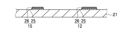
- reference numerals 12 and 15 denote electrodes made of the patterned laminated film 22a
- reference numeral 12 denotes a storage capacitor electrode
- reference numeral 15 denotes a gate electrode. Since the barrier film 25 containing Ni at 50 atomic% or less is disposed on the surface of the gate electrode 15 and the storage capacitor electrode 12 that is in close contact with the glass substrate 21, the gate electrode 15 and the storage capacitor electrode 12 are formed of a glass substrate. Adhesion to 21 is high.
- the metal resistance layer 26 has an electric resistance lower than that of the barrier film 25, and the electric resistance of the gate electrode 15 and the storage capacitor electrode 12 is lower than that of an electrode constituted only by the barrier film 25. Resistance is low.
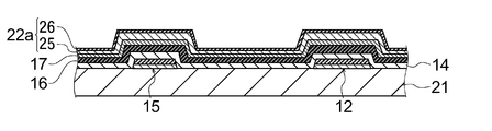
- a gate insulating film 14 made of a silicon nitride thin film (SiN x ), a silicon layer 16 made of amorphous silicon, and an ohmic contact layer 17 are laminated in the order described, and a laminated film 22a is formed on the surface of the ohmic contact layer 17 in the steps of FIGS. 2A and 2B (FIG. 3B).
- a resist (not shown) having an opening of a predetermined shape is disposed on the surface of the laminated film 22a, the laminated film 22a is exposed in the opening, and an etching solution is brought into contact therewith, so that the metal low resistance layer 26 and the barrier film 25 are exposed. Are continuously etched with the same etching solution, and the laminated film 22a is patterned. After the resist is removed, the ohmic contact layer 17 and the silicon layer 16 are patterned to obtain the thin film transistor 20 (FIG. 3C).
- the gate insulating film 14 remains without being etched, the silicon layer 16 remains immediately above and on both sides of the gate electrode 15, and the other portions are removed by etching.
- the ohmic contact layer 17 and the laminated film 22a remain on both sides of the gate electrode 15 and are separated by an opening formed directly above the gate electrode 15, and the first and second ohmic contact layers 31 and 32 and the source and drain electrodes 33 and 34 are formed.
- the reference numeral 30 in the figure indicates a semiconductor layer composed of the remaining silicon layer 16 and the first and second ohmic contact layers 31 and 32.
- the source and drain electrodes 33 and 34 are in close contact with the first and second ohmic contact layers 31 and 32 and are electrically connected to the semiconductor layer 30.
- the silicon layer 16 has the same conductivity type (here, n-type) as the first and second ohmic contact layers 31 and 32, but has a low impurity concentration.
- n-type conductivity type
- the gate electrode 15 When a voltage is applied to the gate electrode 15, a low resistance storage layer is formed in a portion of the silicon layer 16 in contact with the gate electrode 15 via the gate insulating film 14, and the first and second ohmic contacts are formed via the storage layer.
- Contact layers 31 and 32 are electrically connected.
- the silicon layer 16 may have a conductivity type opposite to that of the first and second ohmic contact layers 31 and 32.
- the inversion of the same conductivity type as that of the first and second ohmic contact layers 31 and 32 is applied to a portion of the silicon layer 16 in contact with the gate electrode 15 via the gate insulating film 14.
- a layer is formed, and the first and second ohmic contact layers 31 and 32 are electrically connected by the inversion layer.
- a passivation film 24 made of a silicon nitride thin film is formed on the surface of the glass substrate 21 on which the thin film transistor 20 is formed, and the drain electrode 34 of the passivation film 24 is formed.
- a pixel electrode 27 made of a patterned transparent conductive film is disposed on the passivation film 24 (FIG. 3D).
- the pixel electrode 27 is electrically connected to the drain electrode 34.
- a current flows from the source electrode 33 to the drain electrode 34, and a voltage is applied to the pixel electrode 27.
- the source electrode 33 and the drain electrode 34 are in close contact with the semiconductor layer 30 (first and second ohmic contact layers 31 and 32), respectively, but since the barrier film 25 is disposed in the close contact portion, the source, Copper does not diffuse from the drain electrodes 33 and 34 into the semiconductor layer 30.
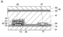
- the liquid crystal display device 50 is formed by arranging the liquid crystal 41 on the pixel electrode 27 of FIG. 3D and arranging the panel 40 on which the counter electrode 45 is formed on the surface of the glass substrate 42 on the liquid crystal 41. .
- the voltage applied to the pixel electrode 27 and the counter electrode 45 can be controlled, and the light transmittance of the liquid crystal 41 can be controlled.
- Reference numeral 60 in FIG. 5 shows a thin film transistor according to a second example of the present invention.
- a single silicon layer 16 constitutes a semiconductor layer.
- the source and drain electrodes 33 and 34 are in direct contact with and electrically connected to the silicon layer 16.
- Reference numeral 70 in FIG. 6 shows a thin film transistor of the third example of the present invention.
- This thin film transistor 70 is a top gate type (stagger type) thin film transistor, and has a semiconductor layer 71 disposed on the glass substrate 21.
- a gate electrode 75 is disposed on the semiconductor layer 71 via a gate oxide film 72.
- An interlayer insulating film 81 is disposed on the gate electrode 75, and the source and drain electrodes 73 and 74 are disposed on the interlayer insulating film 81.
- the source and drain electrodes 73 and 74 are in contact with and electrically connected to the semiconductor layer 71 through through holes formed in the interlayer insulating film 81.
- the source and drain electrodes 73 and 74 are covered with an interlayer insulating film 82.
- a pixel electrode 85 is disposed on the interlayer insulating film 82, and the pixel electrode 85 is connected to the drain electrode 74 through a through hole formed in the interlayer insulating film 82.
- At least one of the electrodes 73 to 75 among the gate electrode 75, the source electrode 73, and the drain electrode 74 is formed of the wiring film of the present invention, and the barrier film 25 is formed in a portion in close contact with the semiconductor layer 71. If the electrode is disposed, the electrodes 73 to 75 are difficult to peel off from the semiconductor layer 71 and copper diffusion into the semiconductor layer 71 is prevented.
- the type and manufacturing method of the silicon layer 16 and the first and second ohmic contact layers 31 and 32 are not particularly limited.
- a silicon layer amorphous silicon layer, polysilicon layer
- those used for the silicon layer of the TFT can be widely used.
- the constituent material of the semiconductor layers 30 and 71 is not limited to silicon, and an oxide semiconductor such as ZnO or In—Ga—Zn—O may be used as the main component of the semiconductor layers 30 and 71.
- the wiring film manufactured by the target 111 of the present invention is not limited to the TFT electrode, and can be used for wiring films of other electronic components such as semiconductor elements and wiring boards.
- the sputtering gas used for sputtering the nickel target 111 and the copper target 112 is not limited to Ar, and Ne, Xe, or the like can also be used.
- the thickness of the metal low resistance layer 26 is not particularly limited. Since the specific resistance of the entire electrode becomes too high, the thickness of the barrier films 25 and 28 is preferably 1/3 or less of the total thickness of the electrode. Further, considering the adhesion to the semiconductor layer and the glass substrate and the diffusion preventing property, the film thickness of the barrier films 25 and 28 is preferably 10 nm or more.
- An etchant (including an etchant and an etching gas) can etch the barrier films 25 and 28 and the metal low-resistance layer 26 and does not dissolve the silicon layer, the glass substrate, and the oxide semiconductor layer (or has an etching rate). It is not particularly limited as long as it is slow. As such an etchant, an etching solution for copper etching can be widely used.
Landscapes
- Chemical & Material Sciences (AREA)
- Engineering & Computer Science (AREA)
- Materials Engineering (AREA)
- Mechanical Engineering (AREA)
- Metallurgy (AREA)
- Organic Chemistry (AREA)
- Inorganic Chemistry (AREA)
- Chemical Kinetics & Catalysis (AREA)
- Thin Film Transistor (AREA)
- Electrodes Of Semiconductors (AREA)
Abstract
信頼性の高い薄膜トランジスタを提供する。薄膜トランジスタ20のゲート電極15、ソースドレイン電極33、34のうち、いずれか一つ以上の電極はバリア膜25を有し、バリア膜25がガラス基板21又は半導体層30に密着している。バリア膜25はNiを50原子%以上含有するので、ガラス基板21や半導体層30に対する密着性が高い。また、バリア膜25表面にCuを主成分とする金属低抵抗層26が形成された場合に、Cuが半導体層30に拡散しない。
Description
本発明は、電子部品向け金属配線膜、その金属配線膜を用いたトランジスタに関するものである。
従来、電子部品用の金属配線膜には、AlやCuなどの低抵抗材料やMo、Cr等が使用されている。たとえばTFT(Thin film transistor、薄膜トランジスタ)液晶ディスプレイではパネルの大型化とともに、配線電極の低抵抗化の要求が大きくなってきており、低抵抗配線としてAlやCuを用いる必要性が高まっている。
TFTで用いられているAl配線では後工程でのヒロック発生や、Al配線をソース、ドレイン電極として用いた場合の下地Si層への拡散の問題、ITO(インジウム・錫酸化物)からなる透明電極とのコンタクト抵抗の劣化などの問題があり、それらを回避するため、MoやCr及びそれらを主成分とする合金膜を前後に積層するバリア層が必要となる。
一方、Cu配線に関しては、CuはAlより低抵抗な材料である。AlはITO透明電極とのコンタクト抵抗の劣化が問題とされるが、Cuは酸化しにくいためコンタクト抵抗も良好である。
従って、Cuを低抵抗配線膜として用いる必要性が高まっている。しかし、Cuは他の配線材料と比べて、ガラスやSi等の下地材料との密着性が悪いという問題や、ソース、ドレイン電極として用いた場合、Si層にCuが拡散するという問題があるため、Cu配線と他の層との界面に密着性の向上や拡散防止のためのバリア層が必要となる。
また半導体で用いられているCuメッキの下地Cuシード層に関しても、上記と同様に拡散の問題から、TiNやTaN等の拡散防止のバリア膜が必要となっている。
特開2002-353222号公報
本発明は上記課題を解決するために成されたものであり、その目的は、拡散防止能と密着性が高いバリア膜を提供することである。
上記課題を解決するために、本発明は、ガラス基板と、シリコン層と、酸化物半導体層とからなる群より選択される少なくとも一つの成膜対象層と接触する配線膜であって、前記配線膜は、前記成膜対象層の表面に密着配置されたバリア膜と、前記バリア膜の表面に密着配置された金属低抵抗層とを有し、前記金属低抵抗層は、Cuを50原子%以上含有し、前記バリア膜は、50原子%以上のNiと、7原子%以上50原子%以下の添加元素とを有し、前記添加元素は、Vと、Alと、Moと、Tiと、Zrと、Crと、Siと、Wと、Taと、Inと、Snと、Znと、Mnと、Cuとからなる添加元素群より選択される配線膜である。
本発明は、ゲート電極と、前記ゲート電極上に配置された半導体層と、前記ゲート電極と前記半導体層の間に配置されたゲート絶縁膜と、前記半導体層に電気的に接続された接続電極とを有する薄膜トランジスタであって、前記接続電極は、前記半導体層に密着配置されたバリア膜と、前記バリア膜の前記半導体層とは反対側の面に密着配置された金属低抵抗層とを有し、前記金属低抵抗層はCuを50原子%以上含有し、前記バリア膜は、50原子%以上のNiと、7原子%以上50原子%以下の添加元素とを有し、前記添加元素は、Vと、Alと、Moと、Tiと、Zrと、Crと、Siと、Wと、Taと、Inと、Snと、Znと、Mnと、Cuとからなる添加元素群より選択される薄膜トランジスタである。
本発明は、ガラス基板上に配置されたゲート電極と、前記ゲート電極上に配置された半導体層と、前記半導体層と前記ゲート電極の間に配置されたゲート絶縁膜とを有する薄膜トランジスタであって、前記ゲート電極は、前記ガラス基板表面に密着配置されたバリア膜と、前記バリア膜の前記ガラス基板と反対側の面に密着配置された金属低抵抗層とを有し、前記金属低抵抗層はCuを50原子%以上含有し、前記バリア膜は、50原子%以上のNiと、7原子%以上50原子%以下の添加元素とを有し、前記添加元素は、Vと、Alと、Moと、Tiと、Zrと、Crと、Siと、Wと、Taと、Inと、Snと、Znと、Mnと、Cuとからなる添加元素群より選択される薄膜トランジスタである。
本発明はターゲットであって、Niを50原子%以上含有し、Vと、Alと、Moと、Tiと、Zrと、Crと、Siと、Wと、Taと、Inと、Snと、Znと、Mnと、Cuとからなる添加元素群より選択されるいずれか1種類以上の添加元素が添加されたターゲットである。
本発明は、ガラス基板と、シリコン層と、酸化物半導体層とからなる群より選択される少なくとも一つの成膜対象層の表面に配線膜を形成する配線膜の形成方法であって、50原子%以上のNiと、7原子%以上50原子%以下の添加元素とを有し、前記添加元素は、Vと、Alと、Moと、Tiと、Zrと、Crと、Siと、Wと、Taと、Inと、Snと、Znと、Mnと、Cuとからなる添加元素群より選択されるターゲットをスパッタリングして、バリア膜を前記成膜対象層に密着形成した後、Cuを50原子%以上含有する銅ターゲットをスパッタリングして、金属低抵抗層を前記バリア膜表面に密着形成する配線膜の形成方法である。
本発明は配線膜の形成方法であって、前記バリア膜と前記金属低抵抗層とを形成した後、同じエッチャントで前記バリア膜と前記金属低抵抗層とをパターニングする配線膜の形成方法である。
本発明は、ゲート電極と、前記ゲート電極上に配置された半導体層と、前記ゲート電極と前記半導体層の間に配置されたゲート絶縁膜と、前記半導体層に電気的に接続された接続電極とを有する薄膜トランジスタであって、前記接続電極は、前記半導体層に密着配置されたバリア膜と、前記バリア膜の前記半導体層とは反対側の面に密着配置された金属低抵抗層とを有し、前記金属低抵抗層はCuを50原子%以上含有し、前記バリア膜は、50原子%以上のNiと、7原子%以上50原子%以下の添加元素とを有し、前記添加元素は、Vと、Alと、Moと、Tiと、Zrと、Crと、Siと、Wと、Taと、Inと、Snと、Znと、Mnと、Cuとからなる添加元素群より選択される薄膜トランジスタである。
本発明は、ガラス基板上に配置されたゲート電極と、前記ゲート電極上に配置された半導体層と、前記半導体層と前記ゲート電極の間に配置されたゲート絶縁膜とを有する薄膜トランジスタであって、前記ゲート電極は、前記ガラス基板表面に密着配置されたバリア膜と、前記バリア膜の前記ガラス基板と反対側の面に密着配置された金属低抵抗層とを有し、前記金属低抵抗層はCuを50原子%以上含有し、前記バリア膜は、50原子%以上のNiと、7原子%以上50原子%以下の添加元素とを有し、前記添加元素は、Vと、Alと、Moと、Tiと、Zrと、Crと、Siと、Wと、Taと、Inと、Snと、Znと、Mnと、Cuとからなる添加元素群より選択される薄膜トランジスタである。
本発明はターゲットであって、Niを50原子%以上含有し、Vと、Alと、Moと、Tiと、Zrと、Crと、Siと、Wと、Taと、Inと、Snと、Znと、Mnと、Cuとからなる添加元素群より選択されるいずれか1種類以上の添加元素が添加されたターゲットである。
本発明は、ガラス基板と、シリコン層と、酸化物半導体層とからなる群より選択される少なくとも一つの成膜対象層の表面に配線膜を形成する配線膜の形成方法であって、50原子%以上のNiと、7原子%以上50原子%以下の添加元素とを有し、前記添加元素は、Vと、Alと、Moと、Tiと、Zrと、Crと、Siと、Wと、Taと、Inと、Snと、Znと、Mnと、Cuとからなる添加元素群より選択されるターゲットをスパッタリングして、バリア膜を前記成膜対象層に密着形成した後、Cuを50原子%以上含有する銅ターゲットをスパッタリングして、金属低抵抗層を前記バリア膜表面に密着形成する配線膜の形成方法である。
本発明は配線膜の形成方法であって、前記バリア膜と前記金属低抵抗層とを形成した後、同じエッチャントで前記バリア膜と前記金属低抵抗層とをパターニングする配線膜の形成方法である。
本発明の配線膜は、半導体層(シリコン層、酸化物半導体層)や透明導電膜やガラス基板に密着する膜、具体的には、TFTのソース電極、ドレイン電極、ゲート電極、蓄積容量電極等の電極に特に適している。また、半導体素子や配線板等の他の電子部品のバリア膜や電極(配線膜)に用いることもできる。
なお、本発明では、シリコン層は、ポリシリコン、アモルファスシリコン等のシリコンを主成分とするものの他に、シリコン層に不純物がドーピングされたもの(オーミックコンタクト層)がある。
バリア膜はNiを50原子%以上含有するから、ガラス基板やシリコン層や酸化物半導体層に対する密着性が、金属低抵抗層よりも高い。バリア膜と金属低抵抗層同士の密着性も高いから、配線膜が成膜対象物から剥離し難い。バリア膜に金属低抵抗層が積層されることで、配線膜の電気抵抗が下がっている。バリア膜と金属低抵抗層を同じエッチャントでエッチング可能であるから、エッチング工程を分ける必要が無く、配線膜及び薄膜トランジスタの製造時間、製造コストが短縮できる。
100……成膜装置 103a……第一の成膜室(真空槽) 111……ニッケルターゲット 15、75……ゲート電極 20、60、70……薄膜トランジスタ 21……成膜対象物(ガラス基板) 25、28……バリア膜 26……金属低抵抗層 33……ソース電極 34……ドレイン電極
図1の符号100は、本発明に用いる成膜装置の一例を示している。
成膜装置100は、搬出入室102と、第一の成膜室103aと、第二の成膜室103bとを有している。搬出入室102と第一の成膜室103aの間と、第一の成膜室103aと第二の成膜室103bの間は、ゲートバルブ109a、109bを介してそれぞれ接続されている。
成膜装置100は、搬出入室102と、第一の成膜室103aと、第二の成膜室103bとを有している。搬出入室102と第一の成膜室103aの間と、第一の成膜室103aと第二の成膜室103bの間は、ゲートバルブ109a、109bを介してそれぞれ接続されている。
搬出入室102と、第一、第二の成膜室103a、103bには、真空排気系113、114a、114bがそれぞれ接続されており、ゲートバルブ109a、109bを閉じ、第一、第二の成膜室103a、103bの内部を真空排気しておく。
次いで、搬出入室102と大気の間の扉を開け、搬出入室102の内部に成膜対象物21を搬入し、扉を閉じ、搬出入室102の内部を真空排気した後、ゲートバルブ109aを開け、成膜対象物21を第一の成膜室103aの内部に移動させ、基板ホルダ108に保持させる。
第一、第二の成膜室103a、103bの内部の底壁側には、本発明のニッケルターゲット111と、銅ターゲット(ここでは銅からなる純銅ターゲット)112がそれぞれ配置されており、成膜対象物21は、各ターゲット111、112と対面できるように、基板ホルダ108に保持される。
第一、第二の成膜室103a、103bにはガス導入系115a、115bがそれぞれ接続されており、第一の成膜室103aの内部を真空排気しながらガス導入系115aからスパッタリングガスを導入し、不図示の電源からニッケルターゲット111に電圧を印加して、スパッタリングする。
ニッケルターゲット111の基板ホルダ108と反対側の面(裏面)には、磁石105(永久磁石又は電磁石)が配置されている。磁石105によりニッケルターゲット111の表面を通る磁力線が形成され、ニッケルターゲット111表面のプラズマ密度が高くなり、磁石105が無い場合に比べてスパッタ速度が速くなる(マグネトロンスパッタ)。
本発明のニッケルターゲット111は、Niの含有量が50%以上であり、Vと、Alと、Moと、Tiと、Zrと、Crと、Siと、Wと、Taと、Inと、Snと、Znと、Mnと、Cuとからなる群より選択されるいずれか一種類以上の非磁性材料が添加元素として添加された合金ターゲットである。
ターゲットがNiのような磁性材料だけで構成されると、マグネトロンスパッタ法で成膜に適した磁界を作るのが困難であるが、本発明のニッケルターゲット111は添加元素が添加されることで非磁性化されているので、マグネトロンスパッタされ、磁石105を配置しない場合に比べてスパッタ速度が速くなる。
ニッケルターゲット111がスパッタリングされると、スパッタ粒子としてニッケル粒子と、添加元素粒子とが放出される。即ち、ニッケルターゲット111からはニッケル原子と添加元素とが放出される。
成膜対象物21の表面(成膜面)19にはガラス層(ガラス基板等)と、シリコン層と、酸化物半導体層のうち、いずれか1種以上の層が露出している。
成膜対象物21は成膜面19をニッケルターゲット111に向けて基板ホルダ108に保持され、ニッケルターゲット111から放出されたスパッタ粒子は成膜面19に入射し、バリア膜25が成膜面19に密着形成される(図2(a))。
成膜対象物21は成膜面19をニッケルターゲット111に向けて基板ホルダ108に保持され、ニッケルターゲット111から放出されたスパッタ粒子は成膜面19に入射し、バリア膜25が成膜面19に密着形成される(図2(a))。
第一の成膜室103aの内部にスパッタガスだけを導入してスパッタリングする場合、バリア膜25の原子組成はニッケルターゲット111の原子組成と略等しくなる。
従って、バリア膜25はNiの含有量が50原子%以上であり、Vと、Alと、Moと、Tiと、Zrと、Crと、Siと、Wと、Taと、Inと、Snと、Znと、Mnと、Cuとからなる群より選択されるいずれか一種類以上の非磁性材料が添加元素として添加されている。
第一の成膜室103aに反応ガス供給系から反応ガス(例えばO2等の酸化性ガス)を供給してスパッタリングをしてもよく、その場合、バリア膜25は、ニッケルと添加元素の他に、反応ガスの構成原子も含有する。
次に、成膜対象物21が保持された基板ホルダ108を第二の成膜室103bに移動させる。第二の成膜室103bを真空排気しながら、ガス導入系115bからスパッタリングガスを導入し、Cuを50原子%以上含有する銅ターゲット(ここでは純銅ターゲット)112をスパッタリングする。
成膜対象物21の表面に、純銅ターゲット112の構成材料である銅原子から成るスパッタリング粒子が到達し、バリア膜25の表面に純銅から成る金属低抵抗層26が形成され、バリア膜25と金属低抵抗層26の積層膜22aが形成される(図2(b))。
金属低抵抗層26の銅含有量が50原子%以上になるのであれば、ニッケル等の他の添加金属が50原子%以下添加された銅ターゲットをスパッタリングして金属低抵抗層26を成膜してもよい。いずれの場合も、金属低抵抗層26はバリア膜25よりも銅含有量が高く、金属低抵抗層26の電気抵抗はバリア膜25の電気抵抗よりも低くなる。
金属低抵抗層26の電気抵抗がバリア膜25より低くなるのであれば、第二の成膜室103bに酸化性ガス等の反応ガスを供給しながら純銅ターゲット112をスパッタリングしてもよい。
積層膜22aはバリア膜25だけで構成してもよいが、バリア膜25を薄膜とし、バリア膜25よりも厚膜の金属低抵抗層26を積層させた方が、全体の電気抵抗が下がる。
積層膜22aはバリア膜25だけで構成してもよいが、バリア膜25を薄膜とし、バリア膜25よりも厚膜の金属低抵抗層26を積層させた方が、全体の電気抵抗が下がる。
また、図2(b)に示す成膜対象物21を第一の成膜室103aに戻し、ニッケルターゲット111をスパッタリングして、金属低抵抗層26の表面にバリア膜28を形成し、金属低抵抗層26と、金属低抵抗層26の表面に形成されたバリア膜25、28とで積層膜22bを構成してもよい。
積層膜22a、22bが形成された成膜対象物21を成膜装置100から搬出する。積層膜22a、22bに所定形状にパターニングされたレジストを配置し、エッチャントで積層膜22a、22bをエッチングする。
ニッケルは銅と同じエッチャント(例えば硝酸を含むエッチング液)でエッチング可能であり、ニッケルのエッチング速度と銅のエッチング速度の差が小さい。従って、金属低抵抗層26とバリア膜25、28は同じエッチャントで連続してエッチングできる。従って、積層膜22a、22bが1回のエッチング工程で所定形状にパターニングされて、電極が形成される。
電極の成膜対象物21と接触する接触面にはバリア膜25が位置する。バリア膜25はニッケルを50原子%以上含有し、ガラス層(ガラス基板)、シリコン層(シリコン半導体層、オーミックコンタクト層)、酸化物半導体層(ZnO、In-Ga-Zn-O)と密着性が高い。
従って、成膜対象物21の表面にガラス層、シリコン層、酸化物半導体層のいずれか1つ以上が露出して、バリア膜25と密着している場合、電極は成膜対象物21の表面から剥がれ難い。
また、ニッケルを50原子%以上含有するバリア膜25は、金属低抵抗層26から半導体層へ銅原子が拡散するのを防止する機能があるから、成膜対象物21の表面にシリコン半導体層、酸化物半導体層等の半導体層が露出する場合に、該半導体層への銅の拡散が防止される。
ニッケルと添加金属であるVとを配合してニッケルターゲット111を形成し、そのニッケルターゲット111の磁性、非磁性を調べた。その結果を、Vの配合量と共に下記表1に記載する。

上記表1に記載したように、添加元素の含有量が7%以上であれば、ニッケルターゲット111が非磁性になることが分かる。
次に、図1の第一の成膜室103a内でニッケルターゲット111をマグネトロンスパッタリングし、成膜対象物21表面に膜厚50nmのバリア膜25を形成した後、純銅ターゲット112をスパッタリングし、バリア膜25の表面に膜厚300nmの金属低抵抗層26が積層された積層膜22aを形成し、図2(b)に示す構造の試験片を得た。
バリア膜25と金属低抵抗層26は、第一、第二の成膜室103a、103bにスパッタリングガス(Arガス)だけを導入し、成膜対象物21を100℃に加熱しながら成膜した。
各試験片の積層膜22aを、エッチング液(硫酸と硝酸と酢酸の混合液)でエッチングし、エッチング特性を調べた。バリア膜25と金属低抵抗層26のエッチング速度の差が小さく、同じエッチング液でエッチング可能であった場合を「○」、エッチング速度の差が大きく、同じエッチング液でエッチングできなかった場合を「×」として上記表1に記載した。
尚、上記表1の「-」は、マグネトロンスパッタリングが正常にできなかったことを示す。これは、添加元素量が少なすぎて、ニッケルターゲット111が非磁性化されなかったためである。
上記表1に記載したように、添加元素の含有量が7原子%以上ではマグネトロンスパッタリングが正常に行われ、更に、添加元素の含有量が50原子%以下ではエッチング特性も良好であった。
上記表1に記載したように、添加元素の含有量が7原子%以上ではマグネトロンスパッタリングが正常に行われ、更に、添加元素の含有量が50原子%以下ではエッチング特性も良好であった。
次に、添加元素の種類を変えてニッケルターゲット111を作成し、そのニッケルターゲット111を用いて積層膜22aを形成し、試験片を作成した。添加元素の種類以外の積層膜22aの形成条件は、上記と同じにした。
各試験片を用いて、上記「エッチング特性」と、下記「密着性」、「バリア性」を調べた。
各試験片を用いて、上記「エッチング特性」と、下記「密着性」、「バリア性」を調べた。
<密着性>
ガラス基板の表面に積層膜22aを形成して試験片とした。試験片の積層膜22aが形成された面に、先端が鋭利なカッタナイフで1mm角のマスを10行×10列、計100個の刻みを入れ、粘着テープ(型番610のスコッチテープ)を貼り付けた後、粘着テープを剥がした時に残存する膜の個数で評価した。全部剥離した場合は0/100、1つも剥離しない場合は100/100となり、90/100以上であれば実用上十分である。
ガラス基板の表面に積層膜22aを形成して試験片とした。試験片の積層膜22aが形成された面に、先端が鋭利なカッタナイフで1mm角のマスを10行×10列、計100個の刻みを入れ、粘着テープ(型番610のスコッチテープ)を貼り付けた後、粘着テープを剥がした時に残存する膜の個数で評価した。全部剥離した場合は0/100、1つも剥離しない場合は100/100となり、90/100以上であれば実用上十分である。
<バリア性>
アモルファスシリコンのシリコン基板の表面に積層膜22aを形成して試験片とした。積層膜22aをエッチング除去した後、シリコン基板の表面を電子顕微鏡で観察し、表面が平滑なものを拡散「○」とし、表面に凹凸が形成されたものを拡散「×」とした。これらの試験結果を、ニッケルターゲット111に添加した添加元素の種類と、その含有量と共に、下記表2に記載する。
アモルファスシリコンのシリコン基板の表面に積層膜22aを形成して試験片とした。積層膜22aをエッチング除去した後、シリコン基板の表面を電子顕微鏡で観察し、表面が平滑なものを拡散「○」とし、表面に凹凸が形成されたものを拡散「×」とした。これらの試験結果を、ニッケルターゲット111に添加した添加元素の種類と、その含有量と共に、下記表2に記載する。
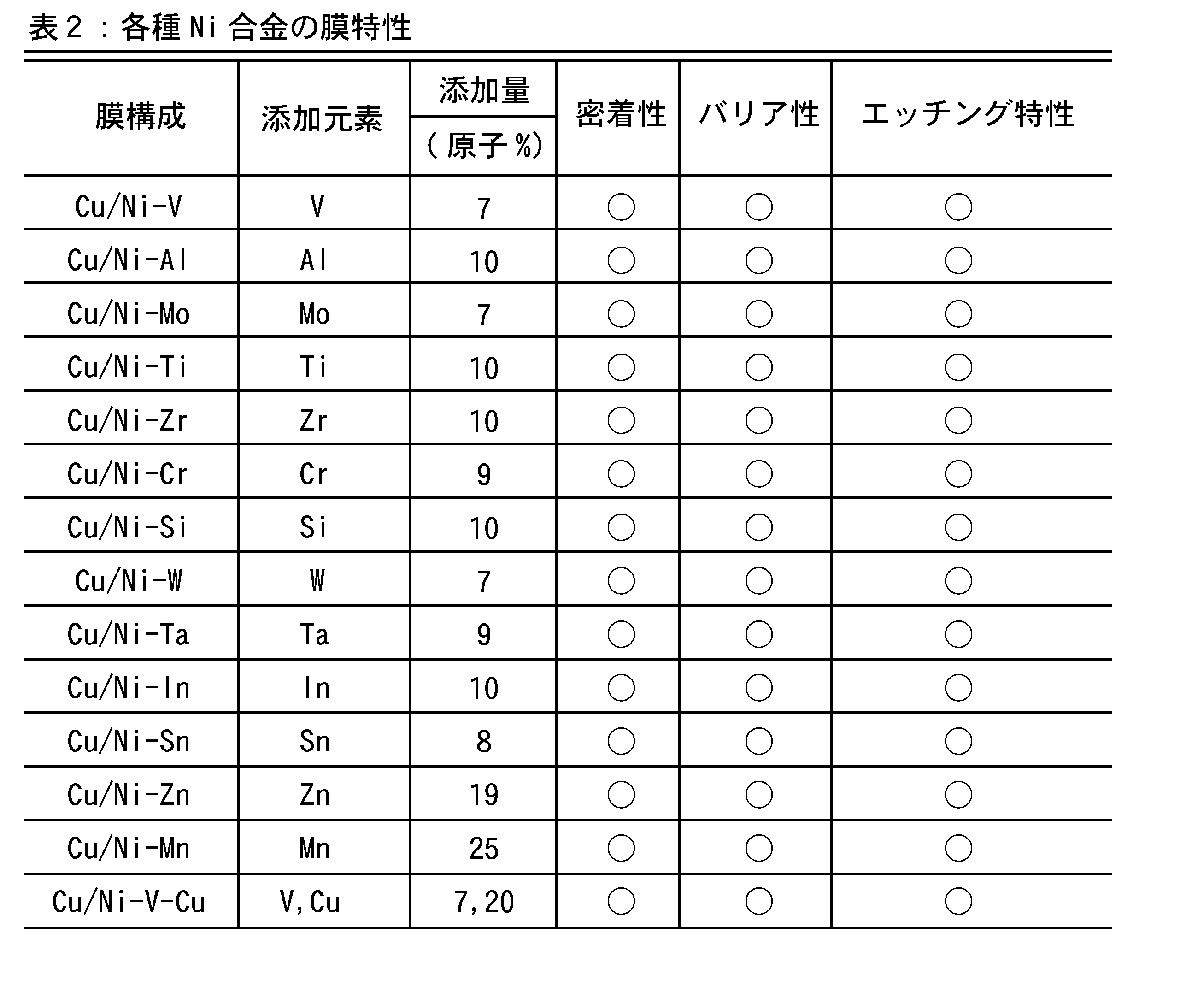
上記表2から分かるように、添加元素として、Vと、Alと、Moと、Tiと、Zrと、Crと、Siと、Wと、Taと、Inと、Snと、Znと、Mnと、Cuのいずれか1種以上をニッケルターゲット111に添加した場合、ガラス基板に対する密着性と、シリコン層に対するバリア性に優れ、しかも、バリア膜25と金属低抵抗層26を同じエッチャントでエッチングすることが可能であった。
また、VとCuのように、ニッケルターゲット111に二種以上の添加元素を添加しても、密着性とバリア性とエッチング特性は変らなかった。
また、VとCuのように、ニッケルターゲット111に二種以上の添加元素を添加しても、密着性とバリア性とエッチング特性は変らなかった。
尚、Vと、Alと、Moと、Tiと、Zrと、Crと、Siと、Wと、Taと、Inと、Snと、Znと、Mnと、Cuの添加量を変えて実験を行ったところ、添加元素の種類が変わっても、添加元素の含有量が50原子%以上であればエッチング特性が良好であり、添加元素の含有量が7原子%未満ではニッケルターゲット111に磁性が残り、マグネトロンスパッタリングが正常に行われなかった。
次に、本発明のニッケルターゲット111を用いて製造される本発明のTFT(薄膜トランジスタ)と、そのTFTを有する電子装置について説明する。
図2(a)、(b)の工程で、成膜対象物21(ここではガラス基板)の表面に積層膜22aを形成する。
図2(a)、(b)の工程で、成膜対象物21(ここではガラス基板)の表面に積層膜22aを形成する。
積層膜22aの表面に所定形状の開口が形成されたレジスト(不図示)を配置し、開口内に積層膜22aを露出させ、エッチング液を接触させる。金属低抵抗層26とバリア膜25は同じエッチング液で連続してエッチング除去され、積層膜22aが所定形状にパターニングされる。
図3(a)の符号12、15はパターニングされた積層膜22aからなる電極を示しており、符号12は蓄積容量電極、符号15はゲート電極を示している。
ゲート電極15と蓄積容量電極12の、ガラス基板21と密着する側の面にはNiを50原子%以下含有するバリア膜25が配置されているから、ゲート電極15と蓄積容量電極12はガラス基板21に対する密着性が高い。
ゲート電極15と蓄積容量電極12の、ガラス基板21と密着する側の面にはNiを50原子%以下含有するバリア膜25が配置されているから、ゲート電極15と蓄積容量電極12はガラス基板21に対する密着性が高い。
また、NiよりもCuの電気抵抗が低いから、金属抵抗層26はバリア膜25よりも電気抵抗が低く、バリア膜25だけで構成した電極に比べて、ゲート電極15と蓄積容量電極12の電気抵抗は低い。
次に、ガラス基板21の蓄積容量電極12及びゲート電極15が形成された面上に、窒化ケイ素薄膜(SiNx)から成るゲート絶縁膜14と、アモルファスシリコンから成るシリコン層16と、オーミックコンタクト層17とを、記載した順番に積層し、オーミックコンタクト層17表面に、図2(a)、(b)の工程で、積層膜22aを形成する(図3(b))。
その積層膜22aの表面に所定形状の開口が形成されたレジスト(不図示)を配置し、開口内に積層膜22aを露出させ、エッチング液を接触させて、金属低抵抗層26とバリア膜25とを同じエッチング液で連続してエッチングし、積層膜22aのパターニングを行う。レジスト除去後、オーミックコンタクト層17とシリコン層16とをパターニングすると、薄膜トランジスタ20が得られる(図3(c))。
この薄膜トランジスタ20では、ゲート絶縁膜14はエッチングされずに残り、シリコン層16はゲート電極15の真上と両側に残り、他の部分はエッチング除去されている。
オーミックコンタクト層17と積層膜22aはゲート電極15の両側に残り、ゲート電極15の真上に形成された開口により分離され、第一、第二のオーミックコンタクト層31、32と、ソース、ドレイン電極33、34が形成される。
同図の符号30は、残ったシリコン層16と、第一、第二のオーミックコンタクト層31、32からなる半導体層を示している。ソース、ドレイン電極33、34は第一、第二のオーミックコンタクト層31、32に密着し、半導体層30に電気的に接続されている。
半導体層30のうち、シリコン層16は第一、第二のオーミックコンタクト層31、32と同じ導電型(ここではn型)であるが、不純物濃度が低い。ゲート電極15に電圧を印加すると、シリコン層16のゲート絶縁膜14を介してゲート電極15と接触する部分に低抵抗な蓄積層が形成され、該蓄積層を介して第一、第二のオーミックコンタクト層31、32が電気的に接続される。
シリコン層16は、第一、第二のオーミックコンタクト層31、32と反対の導電型であってもよい。この場合、ゲート電極15に電圧を印加すると、シリコン層16のゲート絶縁膜14を介してゲート電極15と接触する部分に、第一、第二のオーミックコンタクト層31、32と同じ導電型の反転層が形成され、該反転層によって第一、第二のオーミックコンタクト層31、32が電気的に接続される。
ソース、ドレイン電極33、34を形成した工程の後工程では、ガラス基板21の薄膜トランジスタ20が形成された側の面上に窒化ケイ素薄膜からなるパッシベーション膜24を形成し、パッシベーション膜24のドレイン電極34又はソース電極33(ここではドレイン電極34)や、蓄積容量電極12上を窓開けした後、パッシベーション膜24上に、パターニングした透明導電膜からなる画素電極27を配置する(図3(d))。
画素電極27はドレイン電極34に電気的に接続されている。第一、第二のオーミックコンタクト層31、32を電気的に接続すると、ソース電極33からドレイン電極34に電流が流れ、画素電極27に電圧が印加される。
ソース電極33とドレイン電極34はそれぞれ半導体層30(第一、第二のオーミックコンタクト層31、32)に密着しているが、その密着部分にはバリア膜25が配置されているから、ソース、ドレイン電極33、34から半導体層30に銅が拡散しない。
図4の符号50は、薄膜トランジスタ20を用いた電子装置の一例である液晶表示装置を示している。液晶表示装置50は、図3(d)の画素電極27上に液晶41を配置し、ガラス基板42の表面に対向電極45が形成されたパネル40を、液晶41上に配置して形成される。画素電極27と対向電極45に印加する電圧を制御し、液晶41の光透過率を制御することができる。
以上は、半導体層30がシリコン層16と第一、第二のオーミックコンタクト層31、32に分かれている場合について説明したが、本発明はこれに限定されるものではない。図5の符号60は本発明第二例の薄膜トランジスタを示しており、この薄膜トランジスタ60では、一つのシリコン層16で半導体層が構成される。この場合、ソース、ドレイン電極33、34はシリコン層16に直接接触させて電気的に接続する。
以上は、ゲート電極15がガラス基板21に密着する、所謂ボトムゲート型(逆スタガ型)の薄膜トランジスタについて説明したが、本発明はこれに限定されない。
図6の符号70は本発明第三例の薄膜トランジスタを示しており、この薄膜トランジスタ70は、トップゲート型(スタガ型)薄膜トランジスタであって、ガラス基板21上に配置された半導体層71を有し、該半導体層71上にゲート酸化膜72を介してゲート電極75が配置されている。
ゲート電極75上には層間絶縁膜81が配置され、ソース、ドレイン電極73、74は層間絶縁膜81上に配置されている。層間絶縁膜81に形成された貫通孔を介して、ソース、ドレイン電極73、74が半導体層71に接触し、電気的に接続されている。
ソース、ドレイン電極73、74は層間絶縁膜82で覆われている。その層間絶縁膜82上には画素電極85が配置され、画素電極85は層間絶縁膜82に形成された貫通孔を介してドレイン電極74に接続されている。
この場合も、ゲート電極75と、ソース電極73と、ドレイン電極74のうち、少なくとも1つ以上の電極73~75を本願発明の配線膜で構成し、半導体層71と密着する部分にバリア膜25を配置すれば、電極73~75が半導体層71から剥離し難く、かつ、半導体層71への銅拡散が防止される。
シリコン層16や第一、第二のオーミックコンタクト層31、32の種類や製造方法は特に限定されず、例えば、スパッタリング法や蒸着法等で堆積させたシリコン層(アモルファスシリコン層、ポリシリコン層)等、TFTのシリコン層に用いられるものを広く用いることができる。
半導体層30、71の構成材料はシリコンに限定されず、ZnOやIn-Ga-Zn-O等の酸化物半導体を半導体層30、71の主成分として用いてもよい。
半導体層30、71の構成材料はシリコンに限定されず、ZnOやIn-Ga-Zn-O等の酸化物半導体を半導体層30、71の主成分として用いてもよい。
本発明のターゲット111により製造される配線膜は、TFTの電極に限定されず、半導体素子や配線板等の他の電子部品の配線膜に用いることができる。
ニッケルターゲット111と銅ターゲット112のスパッタリングに用いるスパッタガスはArに限定されず、Ne、Xe等を用いることもできる。
ニッケルターゲット111と銅ターゲット112のスパッタリングに用いるスパッタガスはArに限定されず、Ne、Xe等を用いることもできる。
上述したように、バリア膜25、28と金属低抵抗層26の積層膜で1つの電極や配線を構成する場合、金属低抵抗層26の膜厚は特に限定されないが、膜厚が厚すぎると電極全体の比抵抗が高くなりすぎるので、バリア膜25、28の膜厚は電極全体の膜厚の1/3以下が好ましい。また、半導体層やガラス基板に対する密着性と拡散防止性を考慮すると、バリア膜25、28の膜厚は10nm以上であることが好ましい。
エッチャント(エッチング液、エッチングガスを含む)は、バリア膜25、28と金属低抵抗層26をエッチング可能であって、かつ、シリコン層とガラス基板と酸化物半導体層を溶解しない(又はエッチング速度が遅い)ものであれば特に限定されない。そのようなエッチャントとしては、銅エッチング用のエッチング液を広く用いることができる。
Claims (6)
- ガラス基板と、シリコン層と、酸化物半導体層とからなる群より選択される少なくとも一つの成膜対象層と接触する配線膜であって、
前記配線膜は、前記成膜対象層の表面に密着配置されたバリア膜と、前記バリア膜の表面に密着配置された金属低抵抗層とを有し、
前記金属低抵抗層は、Cuを50原子%以上含有し、
前記バリア膜は、50原子%以上のNiと、7原子%以上50原子%以下の添加元素とを有し、前記添加元素は、Vと、Alと、Moと、Tiと、Zrと、Crと、Siと、Wと、Taと、Inと、Snと、Znと、Mnと、Cuとからなる添加元素群より選択される配線膜。 - ゲート電極と、
前記ゲート電極上に配置された半導体層と、
前記ゲート電極と前記半導体層の間に配置されたゲート絶縁膜と、
前記半導体層に電気的に接続された接続電極とを有する薄膜トランジスタであって、
前記接続電極は、前記半導体層に密着配置されたバリア膜と、前記バリア膜の前記半導体層とは反対側の面に密着配置された金属低抵抗層とを有し、
前記金属低抵抗層はCuを50原子%以上含有し、
前記バリア膜は、50原子%以上のNiと、7原子%以上50原子%以下の添加元素とを有し、前記添加元素は、Vと、Alと、Moと、Tiと、Zrと、Crと、Siと、Wと、Taと、Inと、Snと、Znと、Mnと、Cuとからなる添加元素群より選択される薄膜トランジスタ。 - ガラス基板上に配置されたゲート電極と、
前記ゲート電極上に配置された半導体層と、
前記半導体層と前記ゲート電極の間に配置されたゲート絶縁膜とを有する薄膜トランジスタであって、
前記ゲート電極は、前記ガラス基板表面に密着配置されたバリア膜と、
前記バリア膜の前記ガラス基板と反対側の面に密着配置された金属低抵抗層とを有し、
前記金属低抵抗層はCuを50原子%以上含有し、
前記バリア膜は、50原子%以上のNiと、7原子%以上50原子%以下の添加元素とを有し、前記添加元素は、Vと、Alと、Moと、Tiと、Zrと、Crと、Siと、Wと、Taと、Inと、Snと、Znと、Mnと、Cuとからなる添加元素群より選択される薄膜トランジスタ。 - Niを50原子%以上含有し、
Vと、Alと、Moと、Tiと、Zrと、Crと、Siと、Wと、Taと、Inと、Snと、Znと、Mnと、Cuとからなる添加元素群より選択されるいずれか1種類以上の添加元素が7原子%以上50原子%以下添加されたターゲット。 - ガラス基板と、シリコン層と、酸化物半導体層とからなる群より選択される少なくとも一つの成膜対象層の表面に配線膜を形成する配線膜の形成方法であって、
50原子%以上のNiと、7原子%以上50原子%以下の添加元素とを有し、前記添加元素は、Vと、Alと、Moと、Tiと、Zrと、Crと、Siと、Wと、Taと、Inと、Snと、Znと、Mnと、Cuとからなる添加元素群より選択されるターゲットをスパッタリングして、バリア膜を前記成膜対象層に密着形成した後、
Cuを50原子%以上含有する銅ターゲットをスパッタリングして、金属低抵抗層を前記バリア膜表面に密着形成する配線膜の形成方法。 - 前記バリア膜と前記金属低抵抗層とを形成した後、同じエッチャントで前記バリア膜と前記金属低抵抗層とをパターニングする請求項5記載の配線膜の形成方法。
Applications Claiming Priority (2)
| Application Number | Priority Date | Filing Date | Title |
|---|---|---|---|
| JP2008194665 | 2008-07-29 | ||
| JP2008-194665 | 2008-07-29 |
Publications (1)
| Publication Number | Publication Date |
|---|---|
| WO2010013636A1 true WO2010013636A1 (ja) | 2010-02-04 |
Family
ID=41610335
Family Applications (1)
| Application Number | Title | Priority Date | Filing Date |
|---|---|---|---|
| PCT/JP2009/063185 Ceased WO2010013636A1 (ja) | 2008-07-29 | 2009-07-23 | 配線膜、薄膜トランジスタ、ターゲット、配線膜の形成方法 |
Country Status (2)
| Country | Link |
|---|---|
| TW (1) | TW201013785A (ja) |
| WO (1) | WO2010013636A1 (ja) |
Cited By (7)
| Publication number | Priority date | Publication date | Assignee | Title |
|---|---|---|---|---|
| JP2012222166A (ja) * | 2011-04-08 | 2012-11-12 | Ulvac Japan Ltd | 配線膜、薄膜トランジスタ、ターゲット、配線膜の形成方法 |
| JP2013541192A (ja) * | 2010-09-03 | 2013-11-07 | アプライド マテリアルズ インコーポレイテッド | スタガー薄膜トランジスタおよびその形成方法 |
| JP2013254931A (ja) * | 2012-06-05 | 2013-12-19 | Samsung Display Co Ltd | 薄膜トランジスタ基板 |
| WO2014197661A1 (en) * | 2013-06-06 | 2014-12-11 | H.C. Starck Inc. | Copper-alloy barrier layers and capping layers for metallization in electronic devices |
| JP2015061933A (ja) * | 2013-08-21 | 2015-04-02 | 日立金属株式会社 | 被覆層形成用スパッタリングターゲット材およびその製造方法 |
| WO2015134456A1 (en) * | 2014-03-07 | 2015-09-11 | H.C. Starck Inc. | Etch chemistries for metallization in electronic devices |
| JP2016029216A (ja) * | 2015-09-18 | 2016-03-03 | 住友金属鉱山株式会社 | Cu合金スパッタリングターゲット、この製造方法及び金属薄膜 |
Families Citing this family (1)
| Publication number | Priority date | Publication date | Assignee | Title |
|---|---|---|---|---|
| JP6681019B2 (ja) * | 2015-02-25 | 2020-04-15 | 日立金属株式会社 | 電子部品用積層配線膜および被覆層形成用スパッタリングターゲット材 |
Citations (2)
| Publication number | Priority date | Publication date | Assignee | Title |
|---|---|---|---|---|
| JP2004133422A (ja) * | 2002-09-03 | 2004-04-30 | Lg Philips Lcd Co Ltd | 液晶表示装置用アレイ基板とその製造方法 |
| JP2007242947A (ja) * | 2006-03-09 | 2007-09-20 | Nikko Kinzoku Kk | 半導体配線用バリア膜、半導体用銅配線、同配線の製造方法及び半導体バリア膜形成用スパッタリングターゲット |
-
2009
- 2009-07-23 WO PCT/JP2009/063185 patent/WO2010013636A1/ja not_active Ceased
- 2009-07-28 TW TW098125391A patent/TW201013785A/zh unknown
Patent Citations (2)
| Publication number | Priority date | Publication date | Assignee | Title |
|---|---|---|---|---|
| JP2004133422A (ja) * | 2002-09-03 | 2004-04-30 | Lg Philips Lcd Co Ltd | 液晶表示装置用アレイ基板とその製造方法 |
| JP2007242947A (ja) * | 2006-03-09 | 2007-09-20 | Nikko Kinzoku Kk | 半導体配線用バリア膜、半導体用銅配線、同配線の製造方法及び半導体バリア膜形成用スパッタリングターゲット |
Cited By (19)
| Publication number | Priority date | Publication date | Assignee | Title |
|---|---|---|---|---|
| JP2013541192A (ja) * | 2010-09-03 | 2013-11-07 | アプライド マテリアルズ インコーポレイテッド | スタガー薄膜トランジスタおよびその形成方法 |
| JP2012222166A (ja) * | 2011-04-08 | 2012-11-12 | Ulvac Japan Ltd | 配線膜、薄膜トランジスタ、ターゲット、配線膜の形成方法 |
| JP2013254931A (ja) * | 2012-06-05 | 2013-12-19 | Samsung Display Co Ltd | 薄膜トランジスタ基板 |
| US9929187B2 (en) | 2013-06-06 | 2018-03-27 | H.C. Starck Inc. | Copper-alloy capping layers for metallization in touch-panel displays |
| WO2014197661A1 (en) * | 2013-06-06 | 2014-12-11 | H.C. Starck Inc. | Copper-alloy barrier layers and capping layers for metallization in electronic devices |
| US11640222B2 (en) | 2013-06-06 | 2023-05-02 | Materion Newton, Inc. | Copper-alloy capping layers for metallization in touch-panel displays |
| CN105264669A (zh) * | 2013-06-06 | 2016-01-20 | H·C·施塔克公司 | 用于在电子装置中金属化的铜合金阻挡层和覆盖层 |
| US11392257B2 (en) | 2013-06-06 | 2022-07-19 | Materion Newton Inc. | Copper-alloy capping layers for metallization in touch-panel displays |
| US9299472B2 (en) | 2013-06-06 | 2016-03-29 | H.C. Starck Inc. | Copper-alloy barrier layers for metallization in thin-film transistors and flat panel displays |
| JP2016526233A (ja) * | 2013-06-06 | 2016-09-01 | エイチ.シー. スターク インコーポレイテッド | 電子素子における金属被覆のための銅合金障壁層およびキャッピング層 |
| US10916569B2 (en) | 2013-06-06 | 2021-02-09 | H.C. Starck Inc. | Thin-film transistor and method of forming an electrode of a thin-film transistor |
| JP2015061933A (ja) * | 2013-08-21 | 2015-04-02 | 日立金属株式会社 | 被覆層形成用スパッタリングターゲット材およびその製造方法 |
| US10186530B2 (en) | 2014-03-07 | 2019-01-22 | H.C. Starck Inc. | Etch chemistries for metallization in electronic devices |
| CN106170869A (zh) * | 2014-03-07 | 2016-11-30 | H.C.施塔克公司 | 用于电子装置中的金属化的蚀刻化学成份 |
| CN106170869B (zh) * | 2014-03-07 | 2020-01-10 | H.C.施塔克公司 | 用于电子装置中的金属化的蚀刻化学成份 |
| US9455283B2 (en) | 2014-03-07 | 2016-09-27 | H.C. Starck, Inc. | Etch chemistries for metallization in electronic devices |
| US10923514B2 (en) | 2014-03-07 | 2021-02-16 | H.C. Starck Inc. | Etch chemistries for metallization in electronic devices |
| WO2015134456A1 (en) * | 2014-03-07 | 2015-09-11 | H.C. Starck Inc. | Etch chemistries for metallization in electronic devices |
| JP2016029216A (ja) * | 2015-09-18 | 2016-03-03 | 住友金属鉱山株式会社 | Cu合金スパッタリングターゲット、この製造方法及び金属薄膜 |
Also Published As
| Publication number | Publication date |
|---|---|
| TW201013785A (en) | 2010-04-01 |
Similar Documents
| Publication | Publication Date | Title |
|---|---|---|
| CN101501820B (zh) | 导电膜形成方法、薄膜晶体管、带薄膜晶体管的面板、及薄膜晶体管的制造方法 | |
| JP5017282B2 (ja) | 配線膜の形成方法 | |
| CN101542696B (zh) | 显示装置用Al合金膜、显示装置以及溅射靶材 | |
| KR101795194B1 (ko) | 박막 트랜지스터 및 그의 제조 방법 | |
| TWI395270B (zh) | 配線膜之形成方法、電晶體及電子裝置 | |
| TW200938660A (en) | Etching solution composition | |
| US20120119207A1 (en) | Interconnection structure and method for manufacturing the same, and display device including interconnection structure | |
| CN101512730A (zh) | 导电膜形成方法、薄膜晶体管、带有薄膜晶体管的面板以及薄膜晶体管的制造方法 | |
| TW201131776A (en) | Oxide semiconductor layer and semiconductor device | |
| CN102629609A (zh) | 阵列基板及其制作方法、液晶面板、显示装置 | |
| CN102804352B (zh) | 布线层结构及其制造方法 | |
| JP2014197662A (ja) | 薄膜トランジスタおよびその製造方法 | |
| JP2014239217A (ja) | 半導体装置、半導体装置を有する液晶表示装置、半導体装置の製造方法 | |
| US8361897B2 (en) | Method for depositing a thin film electrode and thin film stack | |
| TW201013785A (en) | Wiring film, thin film transistor, target, and method for forming film transistor | |
| JP2012222166A (ja) | 配線膜、薄膜トランジスタ、ターゲット、配線膜の形成方法 | |
| JP2009280834A (ja) | ターゲット、配線膜形成方法、薄膜トランジスタの製造方法 | |
| JP2008124450A (ja) | ターゲット、成膜方法、薄膜トランジスタ、薄膜トランジスタ付パネル、薄膜トランジスタの製造方法、及び薄膜トランジスタ付パネルの製造方法 | |
| CN101828212B (zh) | 显示装置及该显示装置使用的Cu合金膜 | |
| JP2008112989A (ja) | ターゲット、成膜方法、薄膜トランジスタ、薄膜トランジスタ付パネル、及び薄膜トランジスタの製造方法 | |
| JP2008306043A (ja) | 配線膜の形成方法、トランジスタ、及び電子装置 | |
| JPWO2008149833A1 (ja) | 薄膜トランジスタ製造方法、液晶表示装置製造方法、電極形成方法 | |
| US20210230718A1 (en) | Cu ALLOY TARGET |
Legal Events
| Date | Code | Title | Description |
|---|---|---|---|
| 121 | Ep: the epo has been informed by wipo that ep was designated in this application |
Ref document number: 09802879 Country of ref document: EP Kind code of ref document: A1 |
|
| NENP | Non-entry into the national phase |
Ref country code: DE |
|
| NENP | Non-entry into the national phase |
Ref country code: JP |
|
| 122 | Ep: pct application non-entry in european phase |
Ref document number: 09802879 Country of ref document: EP Kind code of ref document: A1 |