WO2010013611A1 - 無電解銅メッキ方法、プリント配線板、プリント配線板製造方法、半導体装置 - Google Patents
無電解銅メッキ方法、プリント配線板、プリント配線板製造方法、半導体装置 Download PDFInfo
- Publication number
- WO2010013611A1 WO2010013611A1 PCT/JP2009/062979 JP2009062979W WO2010013611A1 WO 2010013611 A1 WO2010013611 A1 WO 2010013611A1 JP 2009062979 W JP2009062979 W JP 2009062979W WO 2010013611 A1 WO2010013611 A1 WO 2010013611A1
- Authority
- WO
- WIPO (PCT)
- Prior art keywords
- resin
- printed wiring
- wiring board
- copper plating
- electroless copper
- Prior art date
- Legal status (The legal status is an assumption and is not a legal conclusion. Google has not performed a legal analysis and makes no representation as to the accuracy of the status listed.)
- Ceased
Links
Classifications
-
- H—ELECTRICITY
- H05—ELECTRIC TECHNIQUES NOT OTHERWISE PROVIDED FOR
- H05K—PRINTED CIRCUITS; CASINGS OR CONSTRUCTIONAL DETAILS OF ELECTRIC APPARATUS; MANUFACTURE OF ASSEMBLAGES OF ELECTRICAL COMPONENTS
- H05K3/00—Apparatus or processes for manufacturing printed circuits
- H05K3/10—Apparatus or processes for manufacturing printed circuits in which conductive material is applied to the insulating support in such a manner as to form the desired conductive pattern
- H05K3/18—Apparatus or processes for manufacturing printed circuits in which conductive material is applied to the insulating support in such a manner as to form the desired conductive pattern using precipitation techniques to apply the conductive material
-
- H—ELECTRICITY
- H05—ELECTRIC TECHNIQUES NOT OTHERWISE PROVIDED FOR
- H05K—PRINTED CIRCUITS; CASINGS OR CONSTRUCTIONAL DETAILS OF ELECTRIC APPARATUS; MANUFACTURE OF ASSEMBLAGES OF ELECTRICAL COMPONENTS
- H05K3/00—Apparatus or processes for manufacturing printed circuits
- H05K3/38—Improvement of the adhesion between the insulating substrate and the metal
- H05K3/381—Improvement of the adhesion between the insulating substrate and the metal by special treatment of the substrate
-
- C—CHEMISTRY; METALLURGY
- C23—COATING METALLIC MATERIAL; COATING MATERIAL WITH METALLIC MATERIAL; CHEMICAL SURFACE TREATMENT; DIFFUSION TREATMENT OF METALLIC MATERIAL; COATING BY VACUUM EVAPORATION, BY SPUTTERING, BY ION IMPLANTATION OR BY CHEMICAL VAPOUR DEPOSITION, IN GENERAL; INHIBITING CORROSION OF METALLIC MATERIAL OR INCRUSTATION IN GENERAL
- C23C—COATING METALLIC MATERIAL; COATING MATERIAL WITH METALLIC MATERIAL; SURFACE TREATMENT OF METALLIC MATERIAL BY DIFFUSION INTO THE SURFACE, BY CHEMICAL CONVERSION OR SUBSTITUTION; COATING BY VACUUM EVAPORATION, BY SPUTTERING, BY ION IMPLANTATION OR BY CHEMICAL VAPOUR DEPOSITION, IN GENERAL
- C23C18/00—Chemical coating by decomposition of either liquid compounds or solutions of the coating forming compounds, without leaving reaction products of surface material in the coating; Contact plating
- C23C18/16—Chemical coating by decomposition of either liquid compounds or solutions of the coating forming compounds, without leaving reaction products of surface material in the coating; Contact plating by reduction or substitution, e.g. electroless plating
-
- C—CHEMISTRY; METALLURGY
- C23—COATING METALLIC MATERIAL; COATING MATERIAL WITH METALLIC MATERIAL; CHEMICAL SURFACE TREATMENT; DIFFUSION TREATMENT OF METALLIC MATERIAL; COATING BY VACUUM EVAPORATION, BY SPUTTERING, BY ION IMPLANTATION OR BY CHEMICAL VAPOUR DEPOSITION, IN GENERAL; INHIBITING CORROSION OF METALLIC MATERIAL OR INCRUSTATION IN GENERAL
- C23C—COATING METALLIC MATERIAL; COATING MATERIAL WITH METALLIC MATERIAL; SURFACE TREATMENT OF METALLIC MATERIAL BY DIFFUSION INTO THE SURFACE, BY CHEMICAL CONVERSION OR SUBSTITUTION; COATING BY VACUUM EVAPORATION, BY SPUTTERING, BY ION IMPLANTATION OR BY CHEMICAL VAPOUR DEPOSITION, IN GENERAL
- C23C18/00—Chemical coating by decomposition of either liquid compounds or solutions of the coating forming compounds, without leaving reaction products of surface material in the coating; Contact plating
- C23C18/16—Chemical coating by decomposition of either liquid compounds or solutions of the coating forming compounds, without leaving reaction products of surface material in the coating; Contact plating by reduction or substitution, e.g. electroless plating
- C23C18/1601—Process or apparatus
- C23C18/1633—Process of electroless plating
- C23C18/1689—After-treatment
- C23C18/1692—Heat-treatment
-
- C—CHEMISTRY; METALLURGY
- C23—COATING METALLIC MATERIAL; COATING MATERIAL WITH METALLIC MATERIAL; CHEMICAL SURFACE TREATMENT; DIFFUSION TREATMENT OF METALLIC MATERIAL; COATING BY VACUUM EVAPORATION, BY SPUTTERING, BY ION IMPLANTATION OR BY CHEMICAL VAPOUR DEPOSITION, IN GENERAL; INHIBITING CORROSION OF METALLIC MATERIAL OR INCRUSTATION IN GENERAL
- C23C—COATING METALLIC MATERIAL; COATING MATERIAL WITH METALLIC MATERIAL; SURFACE TREATMENT OF METALLIC MATERIAL BY DIFFUSION INTO THE SURFACE, BY CHEMICAL CONVERSION OR SUBSTITUTION; COATING BY VACUUM EVAPORATION, BY SPUTTERING, BY ION IMPLANTATION OR BY CHEMICAL VAPOUR DEPOSITION, IN GENERAL
- C23C18/00—Chemical coating by decomposition of either liquid compounds or solutions of the coating forming compounds, without leaving reaction products of surface material in the coating; Contact plating
- C23C18/16—Chemical coating by decomposition of either liquid compounds or solutions of the coating forming compounds, without leaving reaction products of surface material in the coating; Contact plating by reduction or substitution, e.g. electroless plating
- C23C18/18—Pretreatment of the material to be coated
- C23C18/20—Pretreatment of the material to be coated of organic surfaces, e.g. resins
-
- C—CHEMISTRY; METALLURGY
- C23—COATING METALLIC MATERIAL; COATING MATERIAL WITH METALLIC MATERIAL; CHEMICAL SURFACE TREATMENT; DIFFUSION TREATMENT OF METALLIC MATERIAL; COATING BY VACUUM EVAPORATION, BY SPUTTERING, BY ION IMPLANTATION OR BY CHEMICAL VAPOUR DEPOSITION, IN GENERAL; INHIBITING CORROSION OF METALLIC MATERIAL OR INCRUSTATION IN GENERAL
- C23C—COATING METALLIC MATERIAL; COATING MATERIAL WITH METALLIC MATERIAL; SURFACE TREATMENT OF METALLIC MATERIAL BY DIFFUSION INTO THE SURFACE, BY CHEMICAL CONVERSION OR SUBSTITUTION; COATING BY VACUUM EVAPORATION, BY SPUTTERING, BY ION IMPLANTATION OR BY CHEMICAL VAPOUR DEPOSITION, IN GENERAL
- C23C18/00—Chemical coating by decomposition of either liquid compounds or solutions of the coating forming compounds, without leaving reaction products of surface material in the coating; Contact plating
- C23C18/16—Chemical coating by decomposition of either liquid compounds or solutions of the coating forming compounds, without leaving reaction products of surface material in the coating; Contact plating by reduction or substitution, e.g. electroless plating
- C23C18/18—Pretreatment of the material to be coated
- C23C18/20—Pretreatment of the material to be coated of organic surfaces, e.g. resins
- C23C18/2006—Pretreatment of the material to be coated of organic surfaces, e.g. resins by other methods than those of C23C18/22 - C23C18/30
- C23C18/2046—Pretreatment of the material to be coated of organic surfaces, e.g. resins by other methods than those of C23C18/22 - C23C18/30 by chemical pretreatment
- C23C18/2073—Multistep pretreatment
- C23C18/2086—Multistep pretreatment with use of organic or inorganic compounds other than metals, first
-
- C—CHEMISTRY; METALLURGY
- C23—COATING METALLIC MATERIAL; COATING MATERIAL WITH METALLIC MATERIAL; CHEMICAL SURFACE TREATMENT; DIFFUSION TREATMENT OF METALLIC MATERIAL; COATING BY VACUUM EVAPORATION, BY SPUTTERING, BY ION IMPLANTATION OR BY CHEMICAL VAPOUR DEPOSITION, IN GENERAL; INHIBITING CORROSION OF METALLIC MATERIAL OR INCRUSTATION IN GENERAL
- C23C—COATING METALLIC MATERIAL; COATING MATERIAL WITH METALLIC MATERIAL; SURFACE TREATMENT OF METALLIC MATERIAL BY DIFFUSION INTO THE SURFACE, BY CHEMICAL CONVERSION OR SUBSTITUTION; COATING BY VACUUM EVAPORATION, BY SPUTTERING, BY ION IMPLANTATION OR BY CHEMICAL VAPOUR DEPOSITION, IN GENERAL
- C23C18/00—Chemical coating by decomposition of either liquid compounds or solutions of the coating forming compounds, without leaving reaction products of surface material in the coating; Contact plating
- C23C18/16—Chemical coating by decomposition of either liquid compounds or solutions of the coating forming compounds, without leaving reaction products of surface material in the coating; Contact plating by reduction or substitution, e.g. electroless plating
- C23C18/18—Pretreatment of the material to be coated
- C23C18/20—Pretreatment of the material to be coated of organic surfaces, e.g. resins
- C23C18/22—Roughening, e.g. by etching
- C23C18/24—Roughening, e.g. by etching using acid aqueous solutions
-
- C—CHEMISTRY; METALLURGY
- C23—COATING METALLIC MATERIAL; COATING MATERIAL WITH METALLIC MATERIAL; CHEMICAL SURFACE TREATMENT; DIFFUSION TREATMENT OF METALLIC MATERIAL; COATING BY VACUUM EVAPORATION, BY SPUTTERING, BY ION IMPLANTATION OR BY CHEMICAL VAPOUR DEPOSITION, IN GENERAL; INHIBITING CORROSION OF METALLIC MATERIAL OR INCRUSTATION IN GENERAL
- C23C—COATING METALLIC MATERIAL; COATING MATERIAL WITH METALLIC MATERIAL; SURFACE TREATMENT OF METALLIC MATERIAL BY DIFFUSION INTO THE SURFACE, BY CHEMICAL CONVERSION OR SUBSTITUTION; COATING BY VACUUM EVAPORATION, BY SPUTTERING, BY ION IMPLANTATION OR BY CHEMICAL VAPOUR DEPOSITION, IN GENERAL
- C23C18/00—Chemical coating by decomposition of either liquid compounds or solutions of the coating forming compounds, without leaving reaction products of surface material in the coating; Contact plating
- C23C18/16—Chemical coating by decomposition of either liquid compounds or solutions of the coating forming compounds, without leaving reaction products of surface material in the coating; Contact plating by reduction or substitution, e.g. electroless plating
- C23C18/18—Pretreatment of the material to be coated
- C23C18/20—Pretreatment of the material to be coated of organic surfaces, e.g. resins
- C23C18/28—Sensitising or activating
- C23C18/30—Activating or accelerating or sensitising with palladium or other noble metal
-
- C—CHEMISTRY; METALLURGY
- C23—COATING METALLIC MATERIAL; COATING MATERIAL WITH METALLIC MATERIAL; CHEMICAL SURFACE TREATMENT; DIFFUSION TREATMENT OF METALLIC MATERIAL; COATING BY VACUUM EVAPORATION, BY SPUTTERING, BY ION IMPLANTATION OR BY CHEMICAL VAPOUR DEPOSITION, IN GENERAL; INHIBITING CORROSION OF METALLIC MATERIAL OR INCRUSTATION IN GENERAL
- C23C—COATING METALLIC MATERIAL; COATING MATERIAL WITH METALLIC MATERIAL; SURFACE TREATMENT OF METALLIC MATERIAL BY DIFFUSION INTO THE SURFACE, BY CHEMICAL CONVERSION OR SUBSTITUTION; COATING BY VACUUM EVAPORATION, BY SPUTTERING, BY ION IMPLANTATION OR BY CHEMICAL VAPOUR DEPOSITION, IN GENERAL
- C23C18/00—Chemical coating by decomposition of either liquid compounds or solutions of the coating forming compounds, without leaving reaction products of surface material in the coating; Contact plating
- C23C18/16—Chemical coating by decomposition of either liquid compounds or solutions of the coating forming compounds, without leaving reaction products of surface material in the coating; Contact plating by reduction or substitution, e.g. electroless plating
- C23C18/31—Coating with metals
- C23C18/38—Coating with copper
-
- H—ELECTRICITY
- H05—ELECTRIC TECHNIQUES NOT OTHERWISE PROVIDED FOR
- H05K—PRINTED CIRCUITS; CASINGS OR CONSTRUCTIONAL DETAILS OF ELECTRIC APPARATUS; MANUFACTURE OF ASSEMBLAGES OF ELECTRICAL COMPONENTS
- H05K2203/00—Indexing scheme relating to apparatus or processes for manufacturing printed circuits covered by H05K3/00
- H05K2203/07—Treatments involving liquids, e.g. plating, rinsing
- H05K2203/0779—Treatments involving liquids, e.g. plating, rinsing characterised by the specific liquids involved
- H05K2203/0786—Using an aqueous solution, e.g. for cleaning or during drilling of holes
- H05K2203/0789—Aqueous acid solution, e.g. for cleaning or etching
-
- H—ELECTRICITY
- H05—ELECTRIC TECHNIQUES NOT OTHERWISE PROVIDED FOR
- H05K—PRINTED CIRCUITS; CASINGS OR CONSTRUCTIONAL DETAILS OF ELECTRIC APPARATUS; MANUFACTURE OF ASSEMBLAGES OF ELECTRICAL COMPONENTS
- H05K2203/00—Indexing scheme relating to apparatus or processes for manufacturing printed circuits covered by H05K3/00
- H05K2203/11—Treatments characterised by their effect, e.g. heating, cooling, roughening
- H05K2203/1152—Replicating the surface structure of a sacrificial layer, e.g. for roughening
-
- H—ELECTRICITY
- H05—ELECTRIC TECHNIQUES NOT OTHERWISE PROVIDED FOR
- H05K—PRINTED CIRCUITS; CASINGS OR CONSTRUCTIONAL DETAILS OF ELECTRIC APPARATUS; MANUFACTURE OF ASSEMBLAGES OF ELECTRICAL COMPONENTS
- H05K3/00—Apparatus or processes for manufacturing printed circuits
- H05K3/10—Apparatus or processes for manufacturing printed circuits in which conductive material is applied to the insulating support in such a manner as to form the desired conductive pattern
- H05K3/18—Apparatus or processes for manufacturing printed circuits in which conductive material is applied to the insulating support in such a manner as to form the desired conductive pattern using precipitation techniques to apply the conductive material
- H05K3/181—Apparatus or processes for manufacturing printed circuits in which conductive material is applied to the insulating support in such a manner as to form the desired conductive pattern using precipitation techniques to apply the conductive material by electroless plating
-
- H—ELECTRICITY
- H05—ELECTRIC TECHNIQUES NOT OTHERWISE PROVIDED FOR
- H05K—PRINTED CIRCUITS; CASINGS OR CONSTRUCTIONAL DETAILS OF ELECTRIC APPARATUS; MANUFACTURE OF ASSEMBLAGES OF ELECTRICAL COMPONENTS
- H05K3/00—Apparatus or processes for manufacturing printed circuits
- H05K3/40—Forming printed elements for providing electric connections to or between printed circuits
- H05K3/42—Plated through-holes or plated via connections
- H05K3/422—Plated through-holes or plated via connections characterised by electroless plating method; pretreatment therefor
Definitions
- the present invention relates to an electroless copper plating method, a printed wiring board, a printed wiring board manufacturing method, and a semiconductor device.
- a multilayer printed wiring board is manufactured by alternately laminating a circuit and an insulating layer. Specifically, the following methods are mentioned. That is, first, a circuit is formed by etching a copper-clad laminate by a subtractive method or the like, and then an insulating layer is laminated on the circuit. Subsequently, there is a method in which a circuit is formed on the surface of the insulating layer, and further an insulating layer is stacked (for example, described in Patent Document 1). Further, by using a thin copper foil of 5 ⁇ m or less as the copper foil of the copper-clad laminate, it is possible to further miniaturize the multilayer printed wiring board.
- the build-up process by the semi-additive method is attracting attention due to the recent demand for further fine wiring.
- a resin surface is roughened by desmearing, and an electroless copper plating layer is formed on the roughened surface using a palladium catalyst.
- a circuit pattern is formed by electrolytic copper plating.
- the resist is peeled off and the electroless copper plating layer is removed by etching to form fine copper wiring.
- the build-up process by the semi-additive method generally uses a dedicated build-up resin film that assumes the above process flow.
- the desmear process since the smear removal in the laser via hole formed in the build-up layer and the roughening of the resin surface for improving the interfacial adhesion between the resin surface and the electroless copper are performed at the same time, Resin design with desmear resistance has been made.
- the build-up process based on the semi-additive method is advantageous for forming fine wiring, but has a number of limitations on materials.
- JP 2002-305374 A Japanese Patent Laid-Open No. 11-186716
- An object of the present invention is to provide a printed wiring board having high adhesion, high reliability fine copper wiring formed by a semi-additive method on a resin surface obtained by etching a copper foil of a copper clad laminate, Electroless copper plating method capable of manufacturing printed wiring board, method for manufacturing printed wiring board using the electroless copper plating method, printed wiring board manufactured by the manufacturing method, and semiconductor including the printed wiring board A device is provided.
- a method of forming an electroless copper plating layer on a resin surface selected from a resin substrate surface, an insulating resin layer surface, a through-hole wall surface, a via-hole bottom surface, and a via-hole wall surface using a palladium catalyst An electroless copper plating method, wherein a surface to be plated is treated with an acid-based solution as a pretreatment step for performing alkaline degreasing, palladium adsorption, palladium reduction, and electroless copper plating treatment.
- the electroless copper plating method according to [1] wherein the acid-based solution is an aqueous solution containing sulfuric acid.
- a method for producing a printed wiring board comprising a step of forming an electroless copper plating layer using the electroless copper plating method of [1] or [2].
- the copper foil of the copper-clad laminate is etched, and the electroless copper plating layer is applied to the resin base material surface to which the roughened shape of the copper foil is transferred using the electroless copper plating method of [1] or [2].
- the method according to [3] or [4], wherein the printed wiring board manufacturing method [5] includes a step of forming an electroless copper plating after the electroless copper plating, and then a heat treatment is performed Printed wiring board manufacturing method.
- [6] A method for producing a printed wiring board, wherein the heat treatment temperature according to [5] is 200 ° C. or higher.
- the resin composition and / or insulating resin layer of the copper-clad laminate is formed using a resin composition containing at least a cyanate ester resin and a polyfunctional epoxy resin [4] to [4]
- [8] A printed wiring board manufactured by the manufacturing method according to any one of [3] to [7].
- [9] A semiconductor device comprising a semiconductor element mounted on the multilayer printed wiring board according to [8].
- the printed wiring board of the present invention and the method for producing the printed wiring board according to the present invention are obtained by applying a general semi-additive process after acid treatment to the resin surface obtained by etching the copper foil of the copper-clad laminate. Adhesion can be secured. Furthermore, the fine wiring excellent in adhesiveness can be formed by heat-processing after electrolytic copper plating.
- the electroless copper plating method of the present invention comprises etching a resin surface selected from a resin substrate surface, an insulating resin layer, a through-hole wall surface, a via-hole bottom surface and a via-hole wall surface, typically a copper foil of a copper-clad laminate.
- the electroless copper plating step is carried out after performing an acid treatment with an acid-based solution on the surface to be plated after etching the copper foil. .
- the surface of the resin substrate exposed by etching the copper foil of the copper-clad laminate, the surface of the insulating resin layer laminated with the inner layer on which the circuit is formed on the surface of the copper-clad laminate, and the production of the printed wiring board Before performing an electroless copper plating process including alkali degreasing, palladium adsorption, palladium reduction and electroless copper plating on the wall surface of the through hole, the bottom surface of the via hole, and the resin surface of the wall surface provided on the panel,
- the major point of the present invention is that the surface to be plated, which is the subject of electrolytic copper plating, is treated with an acid-based solution.
- sulfuric acid treatment using an aqueous solution containing sulfuric acid as the acid-based solution is preferable, and the concentration of sulfuric acid is preferably 1 to 20% by weight.
- the concentration of sulfuric acid is further preferably 4 to 10% by weight.
- the concentration of the sulfuric acid aqueous solution exceeds 50% by weight, the acidity of the acid-based solution is strong, so that the yield during manufacture of printed wiring boards and the reliability after manufacture are likely to decrease.
- concentration of the sulfuric acid aqueous solution By setting the concentration of the sulfuric acid aqueous solution to 20% by weight or less, palladium serving as a catalyst in electroless plating is likely to adhere to the acid-treated resin surface, and a good electroless copper plating layer is formed. Can do.
- the sulfuric acid may contain hydroxylamine sulfate as an additive.
- the sulfuric acid treatment time is not particularly limited as long as the adhesion and adhesion of the electroless copper plating are ensured, but it is preferably 1 to 10 minutes.
- As the acid in addition to sulfuric acid, hydrochloric acid, nitric acid, and other organic acids may be used.
- the specific treatment method is not particularly limited as long as the acid-based solution can be brought into contact with the surface to be plated, and examples thereof include a method of immersing the copper-clad laminate in the acid-based solution.
- the resin surface selected from the resin base material surface, insulating resin layer surface, through-hole wall surface, via hole bottom surface, and via hole wall surface refers to the resin base material surface, insulating resin layer surface, and through hole.
- the bottom surface of the via hole and the wall surface of the via hole are at least one resin surface, and the object of electroless copper plating layer formation, that is, the object of treatment with an acid-based solution is at least one of the resin surfaces means.
- the printed wiring board manufacturing method of the present invention includes a step of forming an electroless copper plating layer by the electroless copper plating method.
- a typical example is given and demonstrated about the printed wiring board manufacturing method of this invention.
- the copper foil of the double-sided copper-clad laminate is entirely etched using a ferric chloride solution or a cupric chloride solution to obtain a resin base material. That is, the resin surface of the resin base material is exposed.
- the surface roughness of the obtained resin base material can be selected depending on the type of the copper foil of the original copper-clad laminate.
- the roughening of the copper foil can be selected depending on the level of fine wiring.
- through-hole processing and / or via-hole processing may be performed for electrical connection above and below the substrate.
- a mechanical drill, laser processing, or the like may be used for through-hole processing and via-hole processing.
- the through hole processing and the via hole processing may be performed before the copper foil is etched or may be performed after the etching.
- the acid treatment is performed on the resin surface of the obtained resin base material.
- the acid treatment may be a batch type dipping process or a spray type continuous process. It is also possible to adjust the surface roughness of the resin surface onto which the roughened shape of the copper foil has been transferred by the acid treatment (treatment with an acid-based solution). In other words, if the surface roughness of the resin surface obtained by etching is too large, it is possible to obtain a resin surface having a surface roughness suitable for subsequent electroless copper plating by reducing the surface roughness by acid treatment. It is. After the acid treatment step, washing with water and electroless copper plating are performed.
- Electroless copper plating generally comprises a process of cleaner, palladium catalyst application (palladium catalyst adsorption), palladium catalyst reduction, and electroless copper plating treatment.
- the purpose of the cleaner is to remove oils and fats and contaminants attached to the resin surface and to adsorb the surfactant for improving the adhesion of the palladium catalyst thereafter to the resin surface.
- the removal of oils and fats and contaminants in the cleaner is generally performed by alkaline degreasing with an alkaline aqueous solution.
- palladium catalyst application, palladium catalyst reduction treatment, and electroless copper plating treatment are performed to form an electroless copper plating layer on the surface of the resin substrate.
- a photosensitive resist pattern is formed on the surface of the resin base material with the electroless copper plating layer.
- a resist pattern can be formed by laminating an ultraviolet-sensitive dry film resist on the surface of the substrate, selectively sensitizing it with a negative film or the like, and then developing it. Subsequently, after a copper circuit is formed by electrolytic copper plating on the portion where the resist has been removed by development, the resist is peeled off. Finally, the electroless copper plating layer is removed by etching to form a fine circuit pattern.
- a solder resist is formed on the outermost layer, the connection electrode part is exposed so that a semiconductor element can be mounted by exposure and development, a nickel gold plating process is performed, and the multilayer printed wiring board is cut to a predetermined size.
- an insulating resin layer is formed on a fine circuit formed by etching the electroless copper plating layer on the copper-clad laminate, and further, the above electroless copper plating layer formation and resist pattern formation are performed.
- a multilayer printed wiring board in which conductors are further laminated can be obtained by forming a fine circuit through processes such as electrolytic copper plating layer formation.
- a copper circuit is formed by electrolytic copper plating after the electroless copper plating, and then the substrate on which the copper circuit is formed is heat-treated. This is because the peel strength of copper plating can be increased.
- the specific temperature of heat processing is not specifically limited, It is preferable that it is 150 degreeC or more, especially 180 degreeC or more, and also 200 degreeC or more.
- the heat treatment is preferably 300 ° C. or lower, particularly 270 ° C. or lower, and more preferably 250 ° C. or lower from the viewpoint of copper oxidation.
- the resin substrate and / or insulating resin layer of the copper-clad laminate used in the present invention is preferably formed using a resin composition containing a cyanate ester resin.
- a resin composition containing a cyanate ester resin a resin base material (typically containing a glass fiber cloth) or an insulating resin layer having excellent mechanical strength can be obtained.
- the said resin composition contains cyanate ester resin, the effect by the acid treatment using the said acid system solution is high.
- the cyanate ester resin can be obtained, for example, by reacting a cyanogen halide with a phenol and prepolymerizing it by a method such as heating if necessary.
- Specific examples include bisphenol type cyanate resins such as novolac type cyanate resin, bisphenol A type cyanate resin, bisphenol E type cyanate resin, and tetramethylbisphenol F type cyanate resin.
- novolac type cyanate resin is preferable. Thereby, the heat resistance and flame retardance of the resin base material and the insulating resin layer due to an increase in the crosslinking density can be improved. This is because the novolac-type cyanate resin forms a triazine ring after the curing reaction.
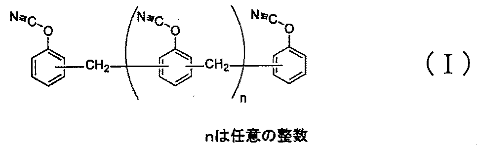
- novolak type cyanate resin for example, those represented by the formula (I) can be used.
- the average repeating unit n of the novolak cyanate resin represented by the formula (I) is not particularly limited, but is preferably 1 to 10, and particularly preferably 2 to 7.
- the average repeating unit n is less than the lower limit, the novolak cyanate resin is easily crystallized, and the solubility in a general-purpose solvent is relatively lowered, which may make handling difficult.
- melt viscosity will become high too much and the moldability of an insulating resin layer may fall.
- the weight average molecular weight of the cyanate ester resin is not particularly limited, but is preferably 5.0 ⁇ 10 2 to 4.5 ⁇ 10 3 , and particularly preferably 6.0 ⁇ 10 2 to 3.0 ⁇ 10 3 . If the weight average molecular weight is less than the lower limit, the mechanical strength of the cured product of the insulating resin layer may be lowered, and when the insulating resin layer is produced, tackiness may occur and the resin may be transferred. There is a case. Further, when the weight average molecular weight exceeds the upper limit, the curing reaction is accelerated, and when used in a multilayer printed wiring board, molding defects may occur or the interlayer peel strength may be reduced. In the present invention, the weight average molecular weight of the resin such as cyanate ester resin can be measured, for example, by GPC (gel permeation chromatography, standard substance: converted to polystyrene).
- the cyanate ester resin including a derivative thereof can be used alone, or two or more having different weight average molecular weights can be used together, or one or two or more, These prepolymers can also be used in combination.
- the content of the cyanate ester resin in the resin composition is not particularly limited, but is preferably 5 to 50% by weight, and particularly preferably 20 to 40% by weight, based on the entire resin composition. If the content is less than the lower limit, it may be difficult to form a resin substrate (preferably containing glass fiber cloth) or an insulating resin layer. If the content exceeds the upper limit, the resin substrate or the insulating resin layer may be formed. There is a case where the strength of the is lowered.
- the resin composition containing the cyanate ester resin preferably contains a polyfunctional epoxy resin (substantially free of halogen atoms).
- the polyfunctional epoxy resin include bisphenol A type epoxy resin, bisphenol F type epoxy resin, bisphenol E type epoxy resin, bisphenol S type epoxy resin, bisphenol M type epoxy resin, bisphenol P type epoxy resin, and bisphenol Z type epoxy resin.
- anthracene type epoxy resin phenoxy type epoxy resin, dicyclopentadiene type epoxy resin, norbornene type epoxy resin, Adama Tan type epoxy resins, fluorene type epoxy resins and the like.
- the polyfunctional epoxy resin one of these can be used alone, or two or more having different weight average molecular weights can be used in combination, or one or two or more of these prepolymers can be used in combination. You can also do it.
- arylalkylene type epoxy resins are particularly preferable. By using an arylalkylene type epoxy resin, the hygroscopic solder heat resistance and flame retardancy of the resin base material and the insulating resin layer can be improved.
- the arylalkylene type epoxy resin refers to an epoxy resin having one or more arylalkylene groups in a repeating unit.
- a xylylene type epoxy resin, a biphenyl dimethylene type epoxy resin, etc. are mentioned.
- a biphenyl dimethylene type epoxy resin is preferable.
- the biphenyl dimethylene type epoxy resin can be represented by, for example, the formula (II).
- the average repeating unit n of the biphenyldimethylene type epoxy resin represented by the formula (II) is not particularly limited, but is preferably 1 to 10, and particularly preferably 2 to 5.
- the average repeating unit n is less than the lower limit, the biphenyldimethylene type epoxy resin is easily crystallized, and the solubility in a general-purpose solvent is relatively lowered, which may make handling difficult.
- the average repeating unit n exceeds the upper limit, the fluidity of the resin is lowered, which may cause molding defects.
- the content of the polyfunctional epoxy resin in the resin composition is not particularly limited, but is preferably 1 to 55% by weight, particularly preferably 2 to 40% by weight, based on the entire resin composition including the cyanate ester resin. If the content is less than the lower limit, the reactivity of the cyanate ester resin may decrease, or the moisture resistance of the resulting product may decrease, and if the content exceeds the upper limit, the resin base material or the insulating resin layer Heat resistance may decrease.
- the weight average molecular weight of the polyfunctional epoxy resin is not particularly limited, but a weight average molecular weight of 5.0 ⁇ 10 2 to 2.0 ⁇ 10 4 is preferable, and 8.0 ⁇ 10 2 to 1.5 ⁇ 10 4 is particularly preferable. preferable. If the weight average molecular weight is less than the lower limit, tackiness may occur in the resin base (typically with glass fiber cloth) or the insulating resin layer. If the upper limit is exceeded, the resin base (typically May be impregnated into the glass substrate (glass fiber cloth) of the resin composition at the time of preparation, and a uniform product may not be obtained.
- the resin composition containing the cyanate ester resin preferably contains a phenol resin.
- the phenol resin include novolak-type phenol resins, resol-type phenol resins, and arylalkylene-type phenol resins. One of these can be used alone, or two or more having different weight average molecular weights can be used in combination, or one or two or more of these prepolymers can be used in combination.
- arylalkylene type phenol resins are particularly preferable. By using an arylalkylene type phenol resin, moisture-absorbing solder heat resistance can be further improved.
- aryl alkylene type phenol resin examples include a xylylene type phenol resin and a biphenyl dimethylene type phenol resin.
- the biphenyl dimethylene type phenol resin can be represented by, for example, the formula (III).
- the repeating unit n of the biphenyldimethylene type phenol resin represented by the formula (III) is not particularly limited, but is preferably 1 to 12, and particularly preferably 2 to 8.
- the average repeating unit n is less than the lower limit, the heat resistance of the biphenyldimethylene type phenol resin may be lowered.
- mold phenol resin and other resin falls, and workability
- operativity may fall.
- the combination of the aforementioned cyanate ester resins (especially novolak-type cyanate resins) and arylalkylene-type phenol resins controls the crosslink density of the resin substrate and insulating resin layer, and easily controls the reactivity of the resin composition during curing. it can.
- the content of the phenol resin in the resin composition is not particularly limited, but is preferably 1 to 55% by weight, and particularly preferably 5 to 40% by weight, based on the entire resin composition.
- the content is less than the lower limit value, the heat resistance of the resin base material or the insulating resin layer may be lowered, and when the upper limit value is exceeded, the low thermal expansion characteristics of the resin base material or the insulating resin layer may be impaired. is there.
- the weight average molecular weight of the phenol resin is not particularly limited, but is preferably 4.0 ⁇ 10 2 to 1.8 ⁇ 10 4 , and particularly preferably 5.0 ⁇ 10 2 to 1.5 ⁇ 10 4 .
- the weight average molecular weight is less than the lower limit value, tackiness may occur in the resin base material (typically with glass fiber cloth) or the insulating resin layer. The impregnation property of the resin composition into the glass substrate (glass fiber cloth) may be reduced, and a uniform product may not be obtained.
- the cyanate ester resin especially novolac type cyanate resin
- the phenol resin arylalkylene type phenolic resin, particularly biphenyldimethylene type phenolic resin
- the polyfunctional epoxy resin arylalkylene type epoxy resin, particularly biphenyldimethylene type.
- the resin composition containing a cyanate ester resin used for a resin base material or an insulating resin layer of a copper-clad laminate preferably contains an inorganic filler. This increases the mechanical strength of the printed wiring board and the semiconductor device even if the thickness of the printed wiring board and the semiconductor device provided with the resin substrate (typically with glass fiber cloth) and the insulating resin layer is thin, and the semiconductor After the device is mounted, warpage when a thermal history such as solder reflow is applied can be more effectively reduced, and the linear expansion coefficient can be further reduced.
- examples of the inorganic filler include silicates such as talc, calcined clay, unfired clay, mica and glass, oxides such as titanium oxide, alumina, silica and fused silica, calcium carbonate, magnesium carbonate, hydrotalcite and the like.
- examples thereof include borates such as calcium oxide and sodium borate, nitrides such as aluminum nitride, boron nitride, silicon nitride, and carbon nitride, titanates such as strontium titanate and barium titanate.
- the inorganic filler one of these can be used alone, or two or more can be used in combination.
- silica is particularly preferable, and fused silica (particularly spherical fused silica) is preferable in terms of excellent low thermal expansion.
- fused silica particularly spherical fused silica
- the shape is crushed or spherical, it can be used according to the purpose such as using spherical silica to lower the melt viscosity of the resin composition in order to ensure the impregnation property to the glass fiber woven fabric.
- the average particle diameter of the inorganic filler is not particularly limited, but is preferably 0.01 to 5.0 ⁇ m, and particularly preferably 0.1 to 2.0 ⁇ m. If the particle size of the inorganic filler is less than the lower limit, the viscosity of the varnish increases, so that the impregnation property of the resin composition into the glass fiber woven fabric may decrease. When the upper limit is exceeded, phenomena such as sedimentation of the inorganic filler may occur in the varnish.
- This average particle diameter can be measured by, for example, a particle size distribution meter (manufactured by HORIBA, LA-500).
- the inorganic filler is not particularly limited, and an inorganic filler having a monodisperse average particle diameter (an inorganic filler having a single average particle diameter or a very narrow distribution of particle diameters) can be used.
- An inorganic filler having a polydispersed diameter inorganic filler having a wide average particle size distribution
- one type of monodispersed and / or polydispersed inorganic filler may be used, or two or more types may be used in combination.
- spherical silica (especially spherical fused silica) having an average particle size of 5.0 ⁇ m or less is preferable, and spherical fused silica having an average particle size of 0.01 to 2.0 ⁇ m is particularly preferable. Thereby, the filling property of an inorganic filler can be improved.
- the content of the inorganic filler is not particularly limited, but is preferably 20 to 80% by weight, particularly preferably 30 to 70% by weight, based on the entire resin composition.
- the resin base material and the insulating resin layer can have particularly low thermal expansion and low water absorption.
- the resin composition containing the cyanate ester resin is not particularly limited, but preferably contains a coupling agent.
- the coupling agent By using the coupling agent, the wettability of the interface between the cyanate ester resin and the inorganic filler can be improved, and the insulating resin and the inorganic filler are uniformly fixed to the glass fiber woven fabric.
- the heat resistance of the resin base material and the insulating resin layer, particularly the solder heat resistance after moisture absorption can be improved.
- the coupling agent is not particularly limited.
- the coupling agent is selected from an epoxy silane coupling agent, a cationic silane coupling agent, an amino silane coupling agent, a titanate coupling agent, and a silicone oil type coupling agent. It is preferable to use one or more coupling agents. Thereby, the wettability with the interface of an inorganic filler can be made high, and thereby heat resistance can be improved more.
- the addition amount of the coupling agent in the resin composition is not particularly limited because it depends on the specific surface area of the inorganic filler, but is preferably 0.05 to 3 parts by weight, particularly 100 parts by weight of the inorganic filler. 0.1 to 2 parts by weight is preferred. If the content is less than the lower limit, the inorganic filler cannot be sufficiently covered with the coupling agent, so the effect of improving the heat resistance of the resin base material or the insulating resin layer may be reduced, and the upper limit is exceeded. This may affect the curing reaction of the cyanate ester resin and may reduce the bending strength of the resin base material and the insulating resin layer.
- a resin composition containing a cyanate ester resin may use a curing accelerator as necessary.
- a well-known thing can be used as said hardening accelerator.
- organic metal salts such as zinc naphthenate, cobalt naphthenate, tin octylate, cobalt octylate, bisacetylacetonate cobalt (II), trisacetylacetonate cobalt (III), triethylamine, tributylamine, diazabicyclo [2,2 , 2] tertiary amines such as octane, 2-phenyl-4-methylimidazole, 2-ethyl-4-ethylimidazole, 2-phenyl-4-methylimidazole, 2-phenyl-4-methyl-5-hydroxyimidazole Imidazoles such as 2-phenyl-4,5-dihydroxyimidazole, phenol compounds such as phenol, bisphenol A, and nonylphenol, organic acids such as
- a semiconductor device can be manufactured by mounting a semiconductor element on a multilayer printed wiring board manufactured by the method described above.
- the mounting method and the sealing method of the semiconductor element are not particularly limited.
- a semiconductor element and a multilayer printed wiring board are used, and a flip-chip bonder or the like is used to align the connection electrode portions on the multilayer printed wiring board and the solder bumps of the semiconductor element.
- the solder bump is heated to the melting point or higher by using an IR reflow device, a hot plate, or other heating device, and the multilayer printed wiring board and the solder bump are connected by fusion bonding.
- a semiconductor device can be obtained by filling and hardening a liquid sealing resin between a multilayer printed wiring board and a semiconductor element.
- Example 1 Copper foil of copper-clad laminate (ELC-9853, manufactured by Sumitomo Bakelite, with 12 ⁇ m copper foil) was etched on both sides with ferric chloride solution, and the resulting resin substrate was immersed in 10% sulfuric acid aqueous solution for 2 minutes. Soaked. Then, it was immersed in an alkali cleaner (Sulcup ACL-009, manufactured by Uemura Kogyo) for 5 minutes, and further immersed in a palladium catalyst treatment solution (ALCUP Activator, manufactured by Uemura Kogyo) for 5 minutes to adsorb the palladium catalyst.
- ELC-9853 manufactured by Sumitomo Bakelite, with 12 ⁇ m copper foil
- the palladium catalyst was subjected to reduction treatment by immersing in a palladium catalyst reduction treatment solution (ALCUP Reducer MAB, manufactured by Uemura Kogyo) for 3 minutes. Thereafter, it was immersed in an electroless copper plating solution (Thru-cup PEA, manufactured by Uemura Kogyo) for 15 minutes to form an electroless copper plating layer.
- AACUP Reducer MAB palladium catalyst reduction treatment solution
- Thru-cup PEA manufactured by Uemura Kogyo
- the obtained substrate on which the electroless copper plating layer was formed was heat-treated at 150 ° C. for 30 minutes, and then subjected to electrolytic copper plating to form a 25 ⁇ m copper layer. Thereafter, heat treatment was performed at 200 ° C. for 60 minutes to obtain a substrate with double-sided plated copper.
- Example 2 A substrate with double-sided plated copper was obtained under the same conditions as in Example 1 except that the treatment was performed at 220 ° C. for 60 minutes after electrolytic copper plating.
- Example 3 A substrate with double-sided plated copper was obtained under the same conditions as in Example 1 except that no heat treatment was performed after electrolytic copper plating.
- Comparative Example 1 A substrate with double-sided plated copper was obtained under the same conditions as in Example 1 except that the substrate was not immersed in a 10% sulfuric acid aqueous solution before being immersed in the alkaline cleaner solution.
- Plating peel A substrate with double-sided plated copper was measured according to JIS C 481.
- Moisture-absorbing solder heat resistance A sample was cut into a 50 mm square from the obtained double-sided plated copper-coated substrate, and half-side etching was performed according to JIS C 6481 to create a test piece. After treatment at 121 ° C. for 2 hours using a pressure cooker, the sample was immersed in 260 ° C. solder for 30 seconds, and the presence or absence of swelling was observed.
- Examples 1 to 3 use the method of the present invention. In all of Examples 1 to 3, adhesion of the electroless copper layer was uniform. In particular, Example 1 and Example 2, in which heat treatment was performed after electrolytic copper plating, showed high peel strength and good moisture absorption heat resistance. Further, in Example 3 in which the heat treatment after electrolytic copper plating was not performed, the peel strength was slightly lower, but the moisture absorption heat resistance test showed good reliability without any abnormality. On the other hand, Comparative Example 1 was not immersed in a 10% aqueous sulfuric acid solution, but the electroless copper layer was unevenly adhered after the electroless copper plating step, and for subsequent electrolytic copper plating and characteristic evaluation. It did not come. From the above results, it is clear that the effect of performing acid treatment before various electroless copper plating steps is clear, and that heat treatment after electrolytic copper plating is also effective for improving adhesion.
Landscapes
- Chemical & Material Sciences (AREA)
- Engineering & Computer Science (AREA)
- Mechanical Engineering (AREA)
- Chemical Kinetics & Catalysis (AREA)
- General Chemical & Material Sciences (AREA)
- Materials Engineering (AREA)
- Metallurgy (AREA)
- Organic Chemistry (AREA)
- Manufacturing & Machinery (AREA)
- Microelectronics & Electronic Packaging (AREA)
- Inorganic Chemistry (AREA)
- Manufacturing Of Printed Wiring (AREA)
- Chemically Coating (AREA)
Abstract
Description
一般に多層プリント配線板は、交互に回路と絶縁層とを積層することで製造される。具体的には、次のような方法が挙げられる。すなわち、まず、サブトラクティブ法等により、銅張り積層板のエッチングにより回路形成を行い、次に、該回路上に絶縁層を積層する。続いてその絶縁層表面に回路を形成し、さらに絶縁層を積層するといった方法が挙げられる(例えば、特許文献1に記載)。
また、銅張り積層板の銅箔として、5μm以下の薄い銅箔を用いることにより、多層プリント配線板の更なる微細化が可能となってきている。
[1] 樹脂基材表面、絶縁樹脂層表面、スルーホール壁面、ビアホールの底面、及びビアホールの壁面から選ばれる樹脂表面に、パラジウム触媒を用いて無電解銅メッキ層を形成する方法であって、
アルカリ脱脂、パラジウム吸着、パラジウム還元、及び無電解銅メッキ処理を行う工程の前処理工程として、被メッキ面を酸系溶液で処理することを特徴とする無電解銅メッキ方法。
[2] 前記酸系溶液が、硫酸を含む水溶液であることを特徴とする[1]に記載の無電解銅メッキ方法。
[3] [1]または[2]の無電解銅メッキ方法を用いて無電解銅メッキ層を形成する工程を含むことを特徴とするプリント配線板製造方法。
[4] 銅張り積層板の銅箔をエッチングし、銅箔の粗化形状が転写した樹脂基材表面に、[1]または[2]の無電解銅メッキ方法を用いて無電解銅メッキ層を形成する工程を含むことを特徴とするプリント配線板製造方法
[5] 無電解銅メッキ後に電解銅メッキを行った後、熱処理を行うことを特徴とする[3]または[4]に記載のプリント配線板製造方法。
[6] [5]記載の熱処理温度が200℃以上であることを特徴とするプリント配線板製造方法。
[7] 銅張り積層板の樹脂組成物及び/又は絶縁樹脂層が、少なくともシアネートエステル樹脂、及び多官能エポキシ樹脂を含む樹脂組成物を用いて形成されていることを特徴とする[4]乃至[6]のいずれかに記載のプリント配線板製造方法。
[8] [3]乃至[7]のいずれかに記載の製造方法で製造されたプリント配線板。
[9] [8]に記載の多層プリント配線板に半導体素子を実装してなる半導体装置。
硫酸中には、添加物として硫酸ヒドロキシルアミンが含まれていてもよい。硫酸処理時間は、無電解銅メッキの付き回りと密着性が確保されれば特に制限するところはないが、1~10分が好ましい。酸としては、硫酸以外に塩酸、硝酸、その他に有機酸であってもよい。また、具体的な処理方法としては、被メッキ面に、酸系溶液を接触させることができれば特に限定されず、例えば、銅張り積層板を酸系溶液に浸漬する方法等が挙げられる。
まず、両面銅張り積層板の銅箔を、塩化第二鉄溶液または塩化第二銅溶液を用いて全面エッチングして樹脂基材を得る。すなわち、樹脂基材の樹脂表面を露出させる。このとき樹脂表面に銅箔の粗化形状が転写されるため、元の銅張り積層板の銅箔の種類によって、得られる樹脂基材の表面粗さを選択することができる。銅箔の粗化としては、微細配線のレベルによって使い分けることができる。このとき、基板上下の電気的接続のために、スルーホール加工及び/又はビアホール加工がされていても良い。スルーホール加工、ビアホール加工は、メカニカルドリル、レーザー加工などを用いるとよい。また、スルーホール加工、ビアホール加工は、銅箔をエッチングする前に実施してもよいし、エッチングした後に実施してもよい。
酸処理工程後に水洗を行い、無電解銅メッキを行う。無電解銅メッキは、一般にクリーナー、パラジウム触媒付与(パラジウム触媒吸着)、パラジウム触媒還元、無電解銅メッキ処理の工程より成る。クリーナーは、樹脂表面に付いた油脂分やコンタミを除去し、その後のパラジウム触媒の付着性を向上させるための界面活性剤を樹脂表面に吸着させることが目的である。クリーナーにおける油脂分やコンタミの除去は、アルカリ性の水溶液によるアルカリ脱脂が一般的である。クリーナーに引き続き、パラジウム触媒付与、パラジウム触媒還元処理、無電解銅メッキ処理を行い、無電解銅メッキ層を樹脂基材表面に形成する。
また、例えば、上記銅張り積層板上の無電解銅メッキ層のエッチングにより形成された微細回路上に、絶縁樹脂層を形成し、さらに、上記したような無電解銅メッキ層形成、レジストパターン形成、電解銅メッキ層形成等の工程を経て、微細回路を形成することで、導体をさらに積層した多層プリント配線板を得ることができる。
本発明において、前記シアネートエステル樹脂等の樹脂の重量平均分子量は、例えばGPC(ゲルパーミエーションクロマトグラフィー、標準物質:ポリスチレン換算)で測定することができる。
多官能エポキシ樹脂としては、これらの中の1種類を単独で用いることもできるし、異なる重量平均分子量を有する2種類以上を併用したり、1種類または2種類以上と、それらのプレポリマーを併用したりすることもできる。
これらの中でも特にアリールアルキレン型エポキシ樹脂が好ましい。アリールアルキレン型エポキシ樹脂を用いることにより、樹脂基材や絶縁樹脂層の吸湿半田耐熱性および難燃性を向上させることができる。


これらの中でも特に、シリカが好ましく、溶融シリカ(特に球状溶融シリカ)が低熱膨張性に優れる点で好ましい。その形状は破砕状、球状があるが、ガラス繊維織布への含浸性を確保するために樹脂組成物の溶融粘度を下げるには球状シリカを使う等、その目的に応じて使用できる。
半導体装置は、上述した方法にて製造された多層プリント配線板に半導体素子を実装し、製造することができる。半導体素子の実装方法、封止方法は特に限定されない。例えば、半導体素子と多層プリント配線板とを用い、フリップチップボンダーなどを用いて多層プリント配線板上の接続用電極部と半導体素子の半田バンプの位置合わせを行う。その後、IRリフロー装置、熱板、その他加熱装置を用いて半田バンプを融点以上に加熱し、多層プリント配線板と半田バンプとを溶融接合することにより接続する。そして、多層プリント配線板と半導体素子との間に液状封止樹脂を充填し、硬化させることで半導体装置を得ることができる。
銅張り積層板(ELC-9853、住友ベークライト製、12μm銅箔付き)の銅箔を塩化第二鉄溶液で両面の銅箔を全面エッチングし、得られた樹脂基板を10%硫酸水溶液に2分間浸漬した。その後、アルカリクリーナー(スルカップ ACL-009、上村工業製)に5分間浸漬し、さらにパラジウム触媒化処理液(ALCUP Activator、上村工業製)に5分間浸漬してパラジウム触媒を吸着させた。続いて、パラジウム触媒還元処理液(ALCUP Reducer MAB、上村工業製)に3分間浸漬してパラジウム触媒の還元処理を行った。その後、無電解銅メッキ液(Thru-cup PEA、上村工業製)に15分間浸漬して無電解銅メッキ層を形成した。
得られた無電解銅メッキ層が形成された基板を150℃で30分間加熱処理した後、電解銅メッキを行い25μmの銅層を形成した。その後、200℃で60分間の熱処理を行い、両面メッキ銅付き基板を得た。
(実施例2)
電解銅メッキ後に220℃で60分処理を行った以外は実施例1と同様の条件で両面メッキ銅付き基板を得た。
(実施例3)
電解銅メッキ後に熱処理を行わなかった以外は、実施例1と同様の条件で両面メッキ銅付き基板を得た。
(比較例1)
アルカリクリーナー液に浸漬する前に、10%硫酸水溶液に浸漬しなかった以外は実施例1と同様の条件で両面メッキ銅付き基板を得た。
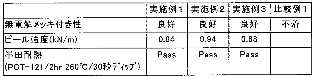
一方、比較例1は、10%硫酸水溶液での浸漬を行わなかったものであるが、無電解銅メッキ工程後に無電解銅層の付着が不均一であり、その後の電解銅メッキ、特性評価に至らなかった。
以上の結果から、各種無電解銅メッキ工程前に酸処理を行う効果は明白であり、また、電解銅メッキ後の熱処理も密着性向上に有効であることは明らかである。
Claims (9)
- 樹脂基材表面、絶縁樹脂層表面、スルーホール壁面、ビアホールの底面、及びビアホールの壁面から選ばれる樹脂表面に、パラジウム触媒を用いて無電解銅メッキ層を形成する方法であって、
アルカリ脱脂、パラジウム吸着、パラジウム還元、及び無電解銅メッキ処理を行う工程の前処理工程として、被メッキ面を酸系溶液で処理することを特徴とする無電解銅メッキ方法。 - 前記酸系溶液が、硫酸を含む水溶液であることを特徴とする請求の範囲第1項に記載の無電解銅メッキ方法。
- 請求の範囲第1項又は第2項に記載の無電解銅メッキ方法を用いて無電解銅メッキ層を形成する工程を含むことを特徴とするプリント配線板製造方法。
- 銅張り積層板の銅箔をエッチングし、銅箔の粗化形状が転写した樹脂基材表面に、請求の範囲第1項又は第2項に記載の無電解銅メッキ方法を用いて無電解銅メッキ層を形成する工程を含むことを特徴とするプリント配線板製造方法。
- 無電解銅メッキ後に電解銅メッキを行った後、熱処理を行うことを特徴とする請求の範囲第3項又は第4項に記載のプリント配線板製造方法。
- 熱処理温度が200℃以上であることを特徴とする請求の範囲第5項に記載のプリント配線板製造方法。
- 銅張り積層板の樹脂基材及び/又は絶縁樹脂層が、シアネートエステル樹脂及び多官能エポキシ樹脂を含む樹脂組成物を用いて形成されていることを特徴とする請求の範囲第4項ないし第6項のいずれかに記載のプリント配線板製造方法。
- 請求の範囲第3項乃至第7項のいずれかに記載の製造方法で製造されたプリント配線板。
- 請求の範囲第8項に記載のプリント配線板に半導体素子を実装してなる半導体装置。
Priority Applications (3)
| Application Number | Priority Date | Filing Date | Title |
|---|---|---|---|
| US13/055,960 US20110120760A1 (en) | 2008-07-30 | 2009-07-17 | Electroless copper plating method, printed wiring board, method for producing the same, and semiconductor device |
| JP2010522679A JPWO2010013611A1 (ja) | 2008-07-30 | 2009-07-17 | 無電解銅メッキ方法、プリント配線板、プリント配線板製造方法、半導体装置 |
| CN2009801291980A CN102106195B (zh) | 2008-07-30 | 2009-07-17 | 非电解镀铜方法、印刷布线板、印刷布线板制造方法、半导体装置 |
Applications Claiming Priority (2)
| Application Number | Priority Date | Filing Date | Title |
|---|---|---|---|
| JP2008-195747 | 2008-07-30 | ||
| JP2008195747 | 2008-07-30 |
Publications (1)
| Publication Number | Publication Date |
|---|---|
| WO2010013611A1 true WO2010013611A1 (ja) | 2010-02-04 |
Family
ID=41610311
Family Applications (1)
| Application Number | Title | Priority Date | Filing Date |
|---|---|---|---|
| PCT/JP2009/062979 Ceased WO2010013611A1 (ja) | 2008-07-30 | 2009-07-17 | 無電解銅メッキ方法、プリント配線板、プリント配線板製造方法、半導体装置 |
Country Status (5)
| Country | Link |
|---|---|
| US (1) | US20110120760A1 (ja) |
| JP (1) | JPWO2010013611A1 (ja) |
| KR (1) | KR20110044207A (ja) |
| CN (1) | CN102106195B (ja) |
| WO (1) | WO2010013611A1 (ja) |
Cited By (1)
| Publication number | Priority date | Publication date | Assignee | Title |
|---|---|---|---|---|
| CN103340023A (zh) * | 2011-01-26 | 2013-10-02 | 住友电木株式会社 | 印刷电路板的制造方法 |
Families Citing this family (7)
| Publication number | Priority date | Publication date | Assignee | Title |
|---|---|---|---|---|
| US8450619B2 (en) * | 2010-01-07 | 2013-05-28 | International Business Machines Corporation | Current spreading in organic substrates |
| JP5681785B2 (ja) * | 2011-02-23 | 2015-03-11 | 東芝三菱電機産業システム株式会社 | 電力変換装置 |
| JP2013104104A (ja) * | 2011-11-14 | 2013-05-30 | Mec Kk | エッチング液、補給液及び銅配線の形成方法 |
| JP6215711B2 (ja) * | 2012-01-11 | 2017-10-18 | 三井金属鉱業株式会社 | 接着剤層付銅箔、銅張積層板及びプリント配線板 |
| CN102625570A (zh) * | 2012-04-27 | 2012-08-01 | 上海贺鸿电子有限公司 | 一种印制线路板及其加成法制造方法 |
| KR102337237B1 (ko) * | 2019-05-08 | 2021-12-08 | 도레이첨단소재 주식회사 | 적층 구조체, 이를 포함하는 연성동박적층필름, 및 상기 적층 구조체의 제작방법 |
| CN113811641B (zh) * | 2019-05-15 | 2023-12-05 | 住友电气工业株式会社 | 印刷布线板 |
Citations (4)
| Publication number | Priority date | Publication date | Assignee | Title |
|---|---|---|---|---|
| JP2001119127A (ja) * | 1999-10-21 | 2001-04-27 | Hitachi Chem Co Ltd | 配線板の製造方法 |
| JP2003198120A (ja) * | 2001-12-27 | 2003-07-11 | Tokai Rubber Ind Ltd | フレキシブルプリント基板およびその製造方法 |
| WO2004080141A1 (ja) * | 2003-03-04 | 2004-09-16 | Zeon Corporation | 多層プリント配線板の製造方法および多層プリント配線板 |
| JP2007227567A (ja) * | 2006-02-22 | 2007-09-06 | Nippon Zeon Co Ltd | 金属薄膜層の形成方法および多層プリント配線板の製造方法 |
Family Cites Families (10)
| Publication number | Priority date | Publication date | Assignee | Title |
|---|---|---|---|---|
| US5047114A (en) * | 1984-11-02 | 1991-09-10 | Amp-Akzo Corporation | Process for the production of metal clad thermoplastic base materials and printed circuits on thermoplastic base materials |
| US4752499A (en) * | 1985-05-16 | 1988-06-21 | Ibiden Co. Ltd. | Adhesive for electroless plating and method of preparation of circuit board using this adhesive |
| US5153987A (en) * | 1988-07-15 | 1992-10-13 | Hitachi Chemical Company, Ltd. | Process for producing printed wiring boards |
| US5648125A (en) * | 1995-11-16 | 1997-07-15 | Cane; Frank N. | Electroless plating process for the manufacture of printed circuit boards |
| MY144574A (en) * | 1998-09-14 | 2011-10-14 | Ibiden Co Ltd | Printed circuit board and method for its production |
| US6793796B2 (en) * | 1998-10-26 | 2004-09-21 | Novellus Systems, Inc. | Electroplating process for avoiding defects in metal features of integrated circuit devices |
| TWI234210B (en) * | 2002-12-03 | 2005-06-11 | Sanyo Electric Co | Semiconductor module and manufacturing method thereof as well as wiring member of thin sheet |
| WO2005122657A1 (ja) * | 2004-06-11 | 2005-12-22 | Ibiden Co., Ltd. | フレックスリジッド配線板とその製造方法 |
| US7989081B2 (en) * | 2006-01-25 | 2011-08-02 | Mitsubishi Gas Chemical Company, Inc. | Resin composite copper foil, printed wiring board, and production processes thereof |
| WO2007122869A1 (ja) * | 2006-04-18 | 2007-11-01 | Okuno Chemical Industries Co., Ltd. | 樹脂成形体に対するエッチング処理用組成物 |
-
2009
- 2009-07-17 KR KR1020117001304A patent/KR20110044207A/ko not_active Ceased
- 2009-07-17 US US13/055,960 patent/US20110120760A1/en not_active Abandoned
- 2009-07-17 JP JP2010522679A patent/JPWO2010013611A1/ja active Pending
- 2009-07-17 CN CN2009801291980A patent/CN102106195B/zh not_active Expired - Fee Related
- 2009-07-17 WO PCT/JP2009/062979 patent/WO2010013611A1/ja not_active Ceased
Patent Citations (4)
| Publication number | Priority date | Publication date | Assignee | Title |
|---|---|---|---|---|
| JP2001119127A (ja) * | 1999-10-21 | 2001-04-27 | Hitachi Chem Co Ltd | 配線板の製造方法 |
| JP2003198120A (ja) * | 2001-12-27 | 2003-07-11 | Tokai Rubber Ind Ltd | フレキシブルプリント基板およびその製造方法 |
| WO2004080141A1 (ja) * | 2003-03-04 | 2004-09-16 | Zeon Corporation | 多層プリント配線板の製造方法および多層プリント配線板 |
| JP2007227567A (ja) * | 2006-02-22 | 2007-09-06 | Nippon Zeon Co Ltd | 金属薄膜層の形成方法および多層プリント配線板の製造方法 |
Cited By (1)
| Publication number | Priority date | Publication date | Assignee | Title |
|---|---|---|---|---|
| CN103340023A (zh) * | 2011-01-26 | 2013-10-02 | 住友电木株式会社 | 印刷电路板的制造方法 |
Also Published As
| Publication number | Publication date |
|---|---|
| KR20110044207A (ko) | 2011-04-28 |
| CN102106195A (zh) | 2011-06-22 |
| US20110120760A1 (en) | 2011-05-26 |
| JPWO2010013611A1 (ja) | 2012-01-12 |
| CN102106195B (zh) | 2013-09-04 |
Similar Documents
| Publication | Publication Date | Title |
|---|---|---|
| CN101652401B (zh) | 环氧树脂组合物、预浸料坯、层叠板、多层印刷线路板、半导体器件、绝缘树脂片、和制造多层印刷线路板的方法 | |
| JP5353241B2 (ja) | 多層プリント配線板および半導体装置 | |
| JP7258453B2 (ja) | 熱硬化性樹脂組成物、キャリア付樹脂膜、プリプレグ、プリント配線基板および半導体装置 | |
| CN102106195B (zh) | 非电解镀铜方法、印刷布线板、印刷布线板制造方法、半导体装置 | |
| JP2010174242A (ja) | ビフェニルアラルキル型シアン酸エステル樹脂、並びにビフェニルアラルキル型シアン酸エステル樹脂を含む樹脂組成物、及び、当該樹脂組成物を用いてなるプリプレグ、積層板、樹脂シート、多層プリント配線板、並びに半導体装置 | |
| JPWO2008093579A1 (ja) | 積層体、基板の製造方法、基板および半導体装置 | |
| JP5533657B2 (ja) | 積層板、回路板および半導体装置 | |
| WO2010092932A1 (ja) | 配線板用樹脂組成物、配線板用樹脂シート、複合体、複合体の製造方法及び半導体装置 | |
| JP2010258415A (ja) | 複合体、複合体の製造方法及び半導体装置 | |
| WO2008099940A9 (ja) | 回路基板の製造方法、半導体製造装置、回路基板及び半導体装置 | |
| JP2003268136A (ja) | プリプレグおよび積層板 | |
| JP5672694B2 (ja) | 樹脂シート、プリント配線板、および半導体装置 | |
| CN102415226A (zh) | 多层印刷电路板的制造方法 | |
| JP2011099072A (ja) | 樹脂組成物、絶縁層、プリプレグ、積層板、プリント配線板および半導体装置 | |
| JP5732729B2 (ja) | 配線板用樹脂組成物、および配線板用樹脂シート | |
| JP2009067852A (ja) | ガラス繊維織布入り絶縁樹脂シート、積層板、多層プリント配線板、及び半導体装置 | |
| JP5929639B2 (ja) | シアン酸エステル化合物、樹脂組成物、プリプレグ、積層板、樹脂シート、多層プリント配線板、および半導体装置 | |
| JP4840303B2 (ja) | ガラス繊維織布入り絶縁樹脂シート、積層板、多層プリント配線板、及び半導体装置 | |
| JP2009206326A (ja) | 多層プリント配線板、及び半導体装置 | |
| JP2004014611A (ja) | 支持体付き絶縁フィルム、多層配線板およびその製造方法 | |
| JP2007189216A (ja) | 多層配線板の製造方法 | |
| JP2002134920A (ja) | 多層プリント配線板および多層プリント配線板の製造方法 | |
| JP5188075B2 (ja) | 回路基板の製造方法及び半導体製造装置 | |
| JP2011254026A (ja) | 複合体の製造方法及び複合体 | |
| JP2008143971A (ja) | 絶縁樹脂組成物、基材付き絶縁樹脂シート、多層プリント配線板、及び、半導体装置 |
Legal Events
| Date | Code | Title | Description |
|---|---|---|---|
| WWE | Wipo information: entry into national phase |
Ref document number: 200980129198.0 Country of ref document: CN |
|
| 121 | Ep: the epo has been informed by wipo that ep was designated in this application |
Ref document number: 09802854 Country of ref document: EP Kind code of ref document: A1 |
|
| WWE | Wipo information: entry into national phase |
Ref document number: 2010522679 Country of ref document: JP |
|
| ENP | Entry into the national phase |
Ref document number: 20117001304 Country of ref document: KR Kind code of ref document: A |
|
| WWE | Wipo information: entry into national phase |
Ref document number: 13055960 Country of ref document: US |
|
| NENP | Non-entry into the national phase |
Ref country code: DE |
|
| 122 | Ep: pct application non-entry in european phase |
Ref document number: 09802854 Country of ref document: EP Kind code of ref document: A1 |