WO2010004875A1 - フレキシブル基板および電気回路構造体 - Google Patents
フレキシブル基板および電気回路構造体 Download PDFInfo
- Publication number
- WO2010004875A1 WO2010004875A1 PCT/JP2009/061505 JP2009061505W WO2010004875A1 WO 2010004875 A1 WO2010004875 A1 WO 2010004875A1 JP 2009061505 W JP2009061505 W JP 2009061505W WO 2010004875 A1 WO2010004875 A1 WO 2010004875A1
- Authority
- WO
- WIPO (PCT)
- Prior art keywords
- wiring pattern
- flexible substrate
- electric circuit
- substrate
- flexible
- Prior art date
- Legal status (The legal status is an assumption and is not a legal conclusion. Google has not performed a legal analysis and makes no representation as to the accuracy of the status listed.)
- Ceased
Links
Images



Classifications
-
- H—ELECTRICITY
- H05—ELECTRIC TECHNIQUES NOT OTHERWISE PROVIDED FOR
- H05K—PRINTED CIRCUITS; CASINGS OR CONSTRUCTIONAL DETAILS OF ELECTRIC APPARATUS; MANUFACTURE OF ASSEMBLAGES OF ELECTRICAL COMPONENTS
- H05K3/00—Apparatus or processes for manufacturing printed circuits
- H05K3/0011—Working of insulating substrates or insulating layers
- H05K3/0044—Mechanical working of the substrate, e.g. drilling or punching
- H05K3/0052—Depaneling, i.e. dividing a panel into circuit boards; Working of the edges of circuit boards
-
- G—PHYSICS
- G02—OPTICS
- G02F—OPTICAL DEVICES OR ARRANGEMENTS FOR THE CONTROL OF LIGHT BY MODIFICATION OF THE OPTICAL PROPERTIES OF THE MEDIA OF THE ELEMENTS INVOLVED THEREIN; NON-LINEAR OPTICS; FREQUENCY-CHANGING OF LIGHT; OPTICAL LOGIC ELEMENTS; OPTICAL ANALOGUE/DIGITAL CONVERTERS
- G02F1/00—Devices or arrangements for the control of the intensity, colour, phase, polarisation or direction of light arriving from an independent light source, e.g. switching, gating or modulating; Non-linear optics
- G02F1/01—Devices or arrangements for the control of the intensity, colour, phase, polarisation or direction of light arriving from an independent light source, e.g. switching, gating or modulating; Non-linear optics for the control of the intensity, phase, polarisation or colour
- G02F1/13—Devices or arrangements for the control of the intensity, colour, phase, polarisation or direction of light arriving from an independent light source, e.g. switching, gating or modulating; Non-linear optics for the control of the intensity, phase, polarisation or colour based on liquid crystals, e.g. single liquid crystal display cells
- G02F1/133—Constructional arrangements; Operation of liquid crystal cells; Circuit arrangements
- G02F1/1333—Constructional arrangements; Manufacturing methods
- G02F1/1345—Conductors connecting electrodes to cell terminals
- G02F1/13452—Conductors connecting driver circuitry and terminals of panels
-
- H—ELECTRICITY
- H05—ELECTRIC TECHNIQUES NOT OTHERWISE PROVIDED FOR
- H05K—PRINTED CIRCUITS; CASINGS OR CONSTRUCTIONAL DETAILS OF ELECTRIC APPARATUS; MANUFACTURE OF ASSEMBLAGES OF ELECTRICAL COMPONENTS
- H05K1/00—Printed circuits
- H05K1/02—Details
- H05K1/0266—Marks, test patterns or identification means
- H05K1/0268—Marks, test patterns or identification means for electrical inspection or testing
-
- H—ELECTRICITY
- H05—ELECTRIC TECHNIQUES NOT OTHERWISE PROVIDED FOR
- H05K—PRINTED CIRCUITS; CASINGS OR CONSTRUCTIONAL DETAILS OF ELECTRIC APPARATUS; MANUFACTURE OF ASSEMBLAGES OF ELECTRICAL COMPONENTS
- H05K1/00—Printed circuits
- H05K1/02—Details
- H05K1/11—Printed elements for providing electric connections to or between printed circuits
- H05K1/118—Printed elements for providing electric connections to or between printed circuits specially for flexible printed circuits, e.g. using folded portions
-
- H—ELECTRICITY
- H05—ELECTRIC TECHNIQUES NOT OTHERWISE PROVIDED FOR
- H05K—PRINTED CIRCUITS; CASINGS OR CONSTRUCTIONAL DETAILS OF ELECTRIC APPARATUS; MANUFACTURE OF ASSEMBLAGES OF ELECTRICAL COMPONENTS
- H05K2201/00—Indexing scheme relating to printed circuits covered by H05K1/00
- H05K2201/03—Conductive materials
- H05K2201/0332—Structure of the conductor
- H05K2201/0388—Other aspects of conductors
- H05K2201/0394—Conductor crossing over a hole in the substrate or a gap between two separate substrate parts
-
- H—ELECTRICITY
- H05—ELECTRIC TECHNIQUES NOT OTHERWISE PROVIDED FOR
- H05K—PRINTED CIRCUITS; CASINGS OR CONSTRUCTIONAL DETAILS OF ELECTRIC APPARATUS; MANUFACTURE OF ASSEMBLAGES OF ELECTRICAL COMPONENTS
- H05K2201/00—Indexing scheme relating to printed circuits covered by H05K1/00
- H05K2201/09—Shape and layout
- H05K2201/09209—Shape and layout details of conductors
- H05K2201/09654—Shape and layout details of conductors covering at least two types of conductors provided for in H05K2201/09218 - H05K2201/095
- H05K2201/09727—Varying width along a single conductor; Conductors or pads having different widths
-
- H—ELECTRICITY
- H05—ELECTRIC TECHNIQUES NOT OTHERWISE PROVIDED FOR
- H05K—PRINTED CIRCUITS; CASINGS OR CONSTRUCTIONAL DETAILS OF ELECTRIC APPARATUS; MANUFACTURE OF ASSEMBLAGES OF ELECTRICAL COMPONENTS
- H05K2201/00—Indexing scheme relating to printed circuits covered by H05K1/00
- H05K2201/10—Details of components or other objects attached to or integrated in a printed circuit board
- H05K2201/10613—Details of electrical connections of non-printed components, e.g. special leads
- H05K2201/10621—Components characterised by their electrical contacts
- H05K2201/10681—Tape Carrier Package [TCP]; Flexible sheet connector
-
- H—ELECTRICITY
- H05—ELECTRIC TECHNIQUES NOT OTHERWISE PROVIDED FOR
- H05K—PRINTED CIRCUITS; CASINGS OR CONSTRUCTIONAL DETAILS OF ELECTRIC APPARATUS; MANUFACTURE OF ASSEMBLAGES OF ELECTRICAL COMPONENTS
- H05K2203/00—Indexing scheme relating to apparatus or processes for manufacturing printed circuits covered by H05K3/00
- H05K2203/15—Position of the PCB during processing
- H05K2203/1545—Continuous processing, i.e. involving rolls moving a band-like or solid carrier along a continuous production path
-
- H—ELECTRICITY
- H05—ELECTRIC TECHNIQUES NOT OTHERWISE PROVIDED FOR
- H05K—PRINTED CIRCUITS; CASINGS OR CONSTRUCTIONAL DETAILS OF ELECTRIC APPARATUS; MANUFACTURE OF ASSEMBLAGES OF ELECTRICAL COMPONENTS
- H05K2203/00—Indexing scheme relating to apparatus or processes for manufacturing printed circuits covered by H05K3/00
- H05K2203/17—Post-manufacturing processes
- H05K2203/175—Configurations of connections suitable for easy deletion, e.g. modifiable circuits or temporary conductors for electroplating; Processes for deleting connections
Definitions
- the present invention relates to a flexible substrate that is punched in a state in which a wiring pattern is formed on a base film and is individually separated, and an electric circuit structure having the flexible substrate and an electric circuit substrate to which the flexible substrate is connected,
- the present invention relates to a flexible substrate and an electric circuit structure that do not cause short-circuit defects caused by wiring pattern chips generated when the flexible substrate is punched.
- a panel substrate constituting a flat panel image display element such as a liquid crystal panel has a pixel electrode constituting one unit of image display on its inner surface, a switching element for applying a predetermined charge to the pixel electrode, metal wiring, etc.
- This is an electric circuit board on which various electric circuit elements are formed.
- an electrode terminal drawn from a metal wiring formed in an image display area where an image is displayed is provided, and a flexible substrate (FPC: Flexible-Printed-Circuits) is provided on the electrode terminal.
- FPC Flexible-Printed-Circuits
- various signals for image display, power supply voltage for operating the panel substrate as an electric circuit substrate, and the like are supplied from a peripheral circuit substrate other than the liquid crystal panel.
- the peripheral circuit substrate is fixed to the back surface of a bottomed frame-shaped mechanism member called a bezel that accommodates a liquid crystal panel or a backlight, and a liquid crystal display as an electric circuit structure
- the device is configured.
- the flexible substrate used for connecting the panel substrate and the peripheral circuit substrate has a predetermined wiring pattern made of a metal foil such as copper foil formed on a flexible base film, and further insulates the surface thereof. It is covered with a sex protective layer.
- the connection portion of the flexible substrate with the panel substrate is provided with an opening in the base film to expose the wiring pattern, and the wiring pattern is in direct contact with the electrode terminal on the panel substrate, so that electrical contact can be obtained.
- the liquid crystal display device also employs a TCP (Tape Carrier Package) in which circuit elements such as a driving semiconductor chip and a capacitor connected to a wiring pattern are mounted on a flexible substrate.
- TCP Transmission Carrier Package
- these flexible substrates are formed continuously in a tape body with a circuit element such as a semiconductor chip mounted thereon. At the time of connection, the tape body is punched into a predetermined shape by a mold and separated individually.
- Patent Document 1 in order to prevent a wiring pattern from being peeled off from a base film and becoming a conductive foreign material due to stress caused by a punching die when a flexible substrate is punched, a short circuit failure between adjacent wiring patterns occurs.
- a technique for providing a wiring pattern having a length that does not reach the punching line at the end of the flexible substrate by alternately changing the length of the wiring pattern is disclosed.
- the chip of the wiring pattern generated when the flexible substrate is punched can be prevented from being short-circuited due to adhering to the end of the flexible substrate. It is impossible to prevent the occurrence of a short circuit defect caused by adhering to another electric circuit substrate connected to a flexible substrate such as a panel substrate.
- the width of the electrode terminals formed on the panel substrate is designed to be as wide as possible, so that the wiring pattern on the flexible substrate formed at the same pitch is more than The interval is narrow. For this reason, since it is inevitable that chips of the wiring pattern are generated when the flexible substrate is punched, it is necessary to sufficiently cope with short-circuit defects on the panel substrate.
- the present invention reduces a short circuit failure caused by wiring pattern chips generated when a flexible substrate is punched, and an electric circuit connected to the flexible substrate.
- An object is to provide an electric circuit structure having a substrate.
- the flexible substrate of the present invention is a flexible substrate in which a wiring pattern is formed on a flexible base film, and the flexible substrate has a wiring pattern formed on the base film.
- the wiring pattern is individually separated by being punched in a state where the wiring film is formed, and the wiring pattern has a narrow portion whose width is narrowed at an end portion of the base film.
- the electric circuit structure of the present invention includes the flexible substrate according to the present invention, and an electric circuit substrate on the surface of which an electric circuit element and electrode terminals connected to the electric circuit element are formed.
- the wiring pattern of the board is connected to the electrode terminal of the electric circuit board.
- the flexible board which prevents the short circuit failure caused by the wiring pattern chips, and the flexible board And an electric circuit structure having an electric circuit board to which the electric circuit board is connected.
- FIG. 1 is a plan view showing a configuration of a flexible substrate according to an embodiment of the present invention.
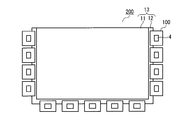
- FIG. 2 is a diagram showing a schematic configuration of the liquid crystal display device according to the embodiment of the present invention.
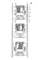
- FIG. 3 is a plan view showing the configuration of the tape body on which the flexible substrate according to the embodiment of the present invention is formed.
- FIG. 4 is a partially enlarged view showing a state before the flexible substrate according to the embodiment of the present invention is punched from the tape body.
- FIG. 5 is a diagram showing the relationship between the wiring pattern of the flexible board according to the embodiment of the present invention and the electrode terminals on the electric circuit board to which the flexible board is connected.
- the flexible substrate according to the present invention is a flexible substrate in which a wiring pattern is formed on a flexible base film, and the flexible substrate is individually punched in a state in which the wiring pattern is formed on the base film. And the wiring pattern has a narrow portion whose width is narrowed at the end of the base film.
- the width of the wiring pattern in the narrow portion is the longest.
- the length of the chips can be shortened as compared with the case where it is not provided. For this reason, even if a flexible substrate is used in a state where chips of a wiring pattern are attached to the flexible substrate, it is possible to effectively prevent occurrence of a short circuit failure caused by the chips.
- the width of the narrow portion is an electrode terminal formed on another electric circuit substrate to which the flexible substrate is connected, and the wiring pattern on the end side having the narrow portion Is preferably narrower than the interval between the electrode terminals connected to each other.
- a circuit element connected to the wiring pattern is mounted. By doing in this way, a flexible substrate can be used as TCP.
- An electric circuit structure according to the present invention includes the flexible substrate according to the present invention, and an electric circuit board on the surface of which an electric circuit element and an electrode terminal connected to the electric circuit element are formed, The wiring pattern of the flexible board is connected to the electrode terminal of the electric circuit board.
- This configuration realizes an electric circuit structure that reduces the occurrence of short-circuit defects caused by chipping of the wiring pattern that occurs when the flexible substrate is punched with the wiring pattern formed on the base film. it can.
- the electric circuit structure is a liquid crystal display device
- the electric circuit substrate is a panel substrate that constitutes a liquid crystal panel and a counter substrate fixed at a predetermined interval across a liquid crystal layer.
- the electric circuit board to which the flexible board of the present invention is connected is not limited to the panel board of a liquid crystal panel, but is used for a wide range of applications such as a panel board of an image display device, an acoustic device and an information processing device. Can be connected to.
- the electric circuit structure of the present invention is not limited to a liquid crystal display device, and can be widely applied to various flat panel display devices such as organic or inorganic EL displays and field emission cold cathode display devices.
- the present invention is not limited to the display device, and can be applied to various modules in which a flexible substrate is connected to an electric circuit substrate such as a driving circuit of an audio device or an information processing device.
- each figure referred below demonstrates only the main member required in order to demonstrate this invention among the structural members of embodiment of this invention, for simplification, and was shown. Therefore, the display apparatus according to the present invention can include arbitrary constituent members that are not shown in each of the referenced drawings. Moreover, the dimension of the member in each figure does not necessarily faithfully represent the dimension of the actual component member, the dimension ratio of each member, and the like.
- FIG. 1 is a plan view showing a configuration of a flexible substrate 100 according to an embodiment of the present invention.
- the flexible substrate 100 of the present invention has a thickness on the surface of a flexible base film 1 having an insulating property such as polyimide having a thickness of about 10 to 50 ⁇ m via an adhesive layer (not shown).
- a predetermined wiring pattern 2 (2a, 2b, 2c) is formed by bonding a metal foil such as a copper foil of about 10 to 50 ⁇ m.
- the wiring pattern 2 is covered with an insulating protective film or protective sheet (not shown), and the flexible substrate 100 has a three-layer structure in which the wiring pattern 2 is sandwiched between the base film 1 and the protective film or protective sheet. ing.
- the flexible substrate 100 of this embodiment is a TCP substrate on which a semiconductor chip 4 that outputs a drive signal for driving a liquid crystal panel is mounted as a circuit element in the center of the substrate.
- the terminal portion 3 formed on the back surface of the semiconductor chip 4, that is, the side facing the wiring pattern 2 of the semiconductor chip 4 is connected through an opening (not shown) provided in the protective sheet to be covered.
- the wiring pattern 2 includes an output-side wiring pattern 2 a connected to the output terminal of the semiconductor chip 4 and an input-side wiring pattern 2 b connected to the input terminal of the semiconductor chip 4.
- the wiring pattern 2a is drawn to the upper end portion of the flexible substrate 100 in FIG. 1, and the input side wiring pattern 2b is drawn to the lower end portion of the flexible substrate 100 in FIG.
- the end portion of the flexible substrate 100 and the vicinity thereof in the output side wiring pattern 2a are narrow portions 2c where the width of the wiring is narrowed.
- the portion where the output side wiring pattern 2a is formed and the portion where the input side wiring pattern 2b is formed are provided with openings 5a, 5b is formed.
- the output-side wiring pattern 2a and the input-side wiring pattern 2b are exposed on the back side in FIG. 1 in the openings 5a and 5b, and this exposed portion is connected to each wiring pattern 2a on the flexible substrate 100, It becomes a connection part of 2b and the electrode terminal formed in the other electric circuit board
- a film material containing conductive particles called ACF (Anisotropic Conductive ⁇ Film) is attached to the opening 5a, and the output side Physical and electrical connection between each wiring of the wiring pattern 2a and a corresponding electrode terminal formed on the panel substrate 12 of the liquid crystal panel 13 is performed.
- the ACF is attached to the opening 5b, and the drive voltage of the driving semiconductor chip 4 and the input signal are generated.
- the physical and electrical contact with the corresponding electrode terminal of the external circuit board (not shown) is generated. A connection is made.
- FIG. 2 is a diagram showing a schematic configuration of a liquid crystal display device 200 described as an example of the electric circuit structure of the present invention.
- the liquid crystal display device 200 of the present embodiment includes a liquid crystal panel in which a glass counter substrate 11 and a glass panel substrate 12 on which electric circuit elements are formed sandwich a liquid crystal layer (not shown). 13 is formed.
- a color filter is formed corresponding to each pixel for displaying a color image, and a counter electrode for applying a predetermined voltage to the liquid crystal layer is formed.
- a plurality of rows and a plurality of columns are formed and pixel electrodes are arranged in a matrix, and by adjusting the potential between the pixel electrode and the counter electrode, Image display is performed by changing the alignment state of the liquid crystal layer. Therefore, the area of the panel substrate 12 where the pixel electrodes are formed becomes the display area of the liquid crystal panel.
- a TFT connected to the electrode is formed.
- illustration regarding the internal structure of these counter substrate 11 and panel substrate 12 is abbreviate
- the panel substrate 12 has a slightly larger surface area than the counter substrate 11, and as shown in FIG. 2, the surface is exposed in both the left and right directions and the lower portion of the liquid crystal panel 13. In the region where the surface is exposed, not shown for applying a predetermined voltage and signal to various wirings such as gate lines and source lines formed on the surface of the panel substrate 12 and electric circuit elements such as TFTs.
- An electrode terminal is formed, and the wiring pattern 2 of the flexible substrate 100 is connected to the electrode terminal by an ACF formed in the opening 5a. In this way, the output signals of the driving semiconductor chip 4 mounted on the flexible substrate 100 are formed on the panel substrate 12 of the liquid crystal panel 13 and each wiring for displaying an image on the liquid crystal panel 13. Will be applied.
- liquid crystal panel 13 is a so-called transmissive panel or transflective panel
- a backlight for irradiating irradiation light necessary for displaying an image on the liquid crystal panel 13 is disposed on the back surface of the liquid crystal panel 13.
- the liquid crystal panel 13 and the backlight are housed in a bezel which is a bottomed frame-like mechanism member to constitute a liquid crystal module as a liquid crystal display device, but illustration thereof in FIG. 2 is omitted.
- the flexible substrate 100 connected to the back panel 12 is shown as it is unfolded around it, but the flexible substrate 100 is a liquid crystal display device.
- the other end is folded back and fixed to the back side of the bezel so as to be along the side surface of the bezel not shown.
- the liquid crystal display device 200 which is an electric circuit structure according to the present invention is not limited to this.
- the case where the flexible substrate 100 is connected to only one side of the panel substrate 12 or the case where the flexible substrate is connected to two sides or all four sides is not excluded. Further, the number of flexible substrates 100 connected to each side of the panel substrate 12 is not limited.
- FIG. 3 is a plan view showing a configuration of the tape body 300 before the flexible substrate 100 of the present embodiment is punched and individually separated.
- the tape body 300 is formed on the flexible resin base material 6 that becomes the base film 1 in a state where the tape body 300 is separated into individual flexible substrates 100, and the wiring pattern 2 (2 a, 2 b). ) And a plurality of semiconductor chips 4 which are mounted circuit elements are continuously formed at a predetermined interval.
- the flexible substrate 100 of the present embodiment is individually separated by punching a plurality of patterns formed on the tape body 300 with a predetermined punching line 7.
- the punching line 7 is a virtual line and corresponds to an outer edge line of a punching die (not shown).
- the wiring pattern 2 formed on the base material 6 of the tape body 300 is extended to the outside of the punching line 7, and each wiring is provided on the extension of the output side wiring pattern 2a and the input side wiring pattern 2b. Inspection pads 8a and 8b wider than the patterns 2a and 2b are formed, respectively. For this reason, in the flexible substrate 100 of this embodiment, before being punched from the tape body 300, the test patterns 8a and 8b are used to form the wiring patterns 2a and 2b and the semiconductor chip 4 which is a mounted circuit element. The electrical characteristics can be inspected.
- the guide portions 9 on both outer sides of the tape body 300 are used when the tape body 300 is wound up or sent out to form the wiring pattern 2, mount the semiconductor chip 4, punch the flexible substrate 100, or the like. An engagement hole 10 is formed.
- FIG. 4 is a partially enlarged plan view showing a region in the vicinity of the punching line 7 on the side where the output-side wiring pattern 2a is formed on the flexible substrate 100 before being punched from the tape body 300.
- FIG. 4 is a partially enlarged plan view showing a region in the vicinity of the punching line 7 on the side where the output-side wiring pattern 2a is formed on the flexible substrate 100 before being punched from the tape body 300.
- a narrow portion 2c having a narrow wiring width is formed at a portion where the output side wiring pattern 2a intersects the punching line 7. That is, in the output side wiring pattern 2a, the wiring width to the portion of the opening 5a formed in the base 6 of the tape body 300 is once narrowed at the narrow portion 2c where the punching line 7 intersects, and thereafter Returning to the original wiring width, the test pad 8a is formed wider at the end portion.
- the output-side wiring pattern 2a is formed at the portion that intersects the punching line 7, that is, the portion that becomes the end portion of the base film 1 after being punched and separated individually. Since the narrow portion 2c is formed, even if wiring pattern chips are generated when punched by the mold, the length of the narrow portion 2c is the maximum.
- the length of the generated chips can be made shorter than the chips that are held.
- the flexible substrate 100 according to the present embodiment is obtained by forming a wiring pattern 2 made of a metal foil on a resin base material 6 to be a base film 1 through an adhesive layer by using a mold. Separated by cutting. At this time, the substrate 6 has a certain flexibility, and the wiring pattern 2 on the adhesive layer also undergoes deformation such as elongation due to the force applied from the mold. Even if the quality is sufficiently controlled, it is not possible to completely prevent the generation of wiring pattern chips during punching.
- the generated chips are likely to adhere to the base film 1 of the flexible substrate 100 that is individually separated by static electricity or the like, it is possible to completely remove the chips from the flexible substrate 100 in the individually separated state. It is extremely difficult.
- the chip of the wiring pattern adhering to the flexible substrate 100 that is unavoidable in practice is mixed in the connection portion between the flexible substrate 100 and another electric circuit substrate, it straddles between adjacent electrode terminals.
- the length of the chip of the wiring pattern generated at the time of punching can be shortened as described above, so that this chip is between adjacent electrode terminals. The possibility of straddling is reduced, and the occurrence of a short circuit failure can be effectively prevented.
- the chip length is simply shortened, it can be realized by narrowing the width of the wiring pattern 2 itself.
- the width of the wiring pattern 2 is too narrow, the strength of the wiring pattern 2 becomes weak, and it becomes difficult to form a predetermined shape on the base film 1.
- the width of the wiring pattern 2 is narrow, when the wiring pattern 2 and the electrode terminal formed on another electric circuit board are connected, the contact area between the two electrodes cannot be taken sufficiently, There is a risk of poor continuity.
- the conductive particles of the ACF are less likely to contact the wiring pattern 2 and the possibility of poor continuity increases. End up. For this reason, as shown in FIG.
- the output side wiring pattern 2a is a predetermined wiring pattern in a portion where the opening 5a is formed, which is a connection portion with at least an electrode terminal formed on another electric circuit board. It is preferable to form the narrow portion 2 c at the end of the base film 1 of the flexible substrate 100 that has a width and intersects the punching line 7.
- FIG. 5 shows the relationship between the end of the flexible substrate 100 and the electrode terminals 14 formed on the panel substrate 12 which is an electric circuit substrate to which the flexible substrate 100 is connected.
- the pitch P2 of the output side wiring pattern 2a on the flexible substrate 100 and the pitch P1 of the electrode terminals 14 on the panel substrate 12 to which the output side wiring pattern 2a is connected are the same interval.
- the width D of the electrode terminal 14 is formed wider than the width A of the output-side wiring pattern 2a in order to prevent a reduction in the conductive area caused by a shift in alignment of the flexible substrate 100 or a shift due to expansion / contraction.
- the interval E between the electrode terminals 14 is smaller than the interval B of the output side wiring pattern 2a.
- the pitch P2 of the output side wiring pattern 2a and the pitch P1 of the electrode terminals 14 are both 50 ⁇ m, the width A and the interval B of the output side wiring pattern 2a In many cases, the width D of the electrode terminal 14 is widened such that the width D of the electrode terminal 14 is 35 ⁇ m and the interval E is 15 ⁇ m.
- the width C of the narrow portion 2c of the output side wiring pattern 2a is set to a value smaller than the interval E between the electrode terminals 14, for example, 13 ⁇ m which is half the width of the output side wiring pattern 2a in the above numerical example.
- the length C is shorter than the interval E between the electrode terminals 14.
- the chips of this wiring pattern do not cause a short circuit failure across the adjacent electrode terminals 14. Therefore, even when the distance E between the electrode terminals 14 is smaller than the width A of the output-side wiring pattern 2a because the width D of the electrode terminal 14 is increased, the occurrence of a short-circuit failure caused by chips of the wiring pattern 2 occurs. Can be effectively prevented.
- the flexible substrate 100 has been described as a TCP substrate on which the semiconductor chip 4 that is a circuit element is mounted.
- the present invention is not limited to this, and the circuit element Even if the flexible substrate 100 is not mounted, the same effect can be achieved by the configuration of the present invention.
- the inspection pads 8a and 8b are not essential in the present invention.
- the wiring pattern 2 intersects the punching line 7, if the narrow portion 2c is formed at the intersecting portion, the effect of the present invention is exhibited. Therefore, as shown in FIG. 4, the width of the wiring pattern 2 does not return from the narrow portion 2 c to the original width outside the intersection of the wiring pattern 2 and the punching line 7. Needless to say, it should be understood as an embodiment of the present invention even if it is terminated.
- the present invention relates to a flexible board that is punched in a state in which a wiring pattern is formed and is individually separated, and an electric circuit board comprising the flexible board and an electric circuit board to which the flexible board is connected. Besides being used as a liquid crystal display device which is a panel substrate constituting a liquid crystal panel, it can be industrially used as a module having an electric circuit substrate for various uses.
Landscapes
- Engineering & Computer Science (AREA)
- Manufacturing & Machinery (AREA)
- Microelectronics & Electronic Packaging (AREA)
- Structure Of Printed Boards (AREA)
- Liquid Crystal (AREA)
Abstract
フレキシブル基板の打ち抜き時に発生する、回路パターンの切り屑が原因となる短絡不良を低減させたフレキシブル基板、および、このフレキシブル基板とこれが接続された電気回路基板とを有する電気回路構造体を提供すること。可撓性のベースフィルム(1)上に配線パターン(2)が形成されたフレキシブル基板(100)であって、前記フレキシブル基板(100)は、前記ベースフィルム(1)上に配線パターン(2)が形成された状態で打ち抜かれて個別に分離されたものであり、かつ、前記配線パターン(2)は、前記ベースフィルム(1)の端部でその幅が狭くなる幅狭部(2c)を有している。
Description
本発明は、ベースフィルム上に配線パターンが形成された状態で打ち抜かれて、個別に分離されるフレキシブル基板、および、このフレキシブル基板とこれが接続される電気回路基板とを有する電気回路構造体に関し、特に、フレキシブル基板の打ち抜き時に生じる配線パターンの切り屑が原因となる短絡不良が生じないフレキシブル基板および電気回路構造体に関する。
液晶パネルなどの平板型画像表示素子を構成するパネル基板は、その内側表面に、画像表示の一単位を構成する画素電極や、画素電極に所定の電荷を印加するためのスイッチング素子、金属配線など、各種電気回路素子が形成された電気回路基板となっている。
液晶パネルのパネル基板の端部近傍には、画像が表示される画像表示領域に形成された金属配線から引き出された電極端子が設けられていて、この電極端子にフレキシブル基板(FPC:Flexible Printed Circuits)が接続され、液晶パネル以外の周辺回路基板などから画像表示のための各種信号や、パネル基板が電気回路基板として動作するための電源電圧などが供給される。また、フレキシブル基板が折り曲げられることで、周辺回路基板が、液晶パネルやバックライトが収容されるベゼルと称される有底枠状の機構部材の背面に固着され、電気回路構造体としての液晶表示装置が構成される。
ここで、パネル基板と周辺回路基板との接続に用いられるフレキシブル基板は、可撓性を有するベースフィルム上に、銅箔などの金属箔からなる所定の配線パターンが形成され、さらにその表面を絶縁性の保護層で覆ったものである。フレキシブル基板のパネル基板との接続部は、ベースフィルムに開口が設けられることで配線パターンを露出させ、配線パターンがパネル基板上の電極端子と直接接触するようにして、電気的なコンタクトが得られる。また、液晶表示装置では、フレキシブル基板上に、配線パターンに接続された駆動用の半導体チップやコンデンサなどの回路素子が搭載される、TCP(Tape Carrier Package)も採用されている。
その取り扱いの容易性を確保するため、これらのフレキシブル基板は、TCPの場合は半導体チップなどの回路素子が搭載された状態で、テープ体に複数個が連続して形成されていて、パネル基板との接続時にテープ体から金型によって所定形状に打ち抜かれて個別に分離される。
特許文献1には、フレキシブル基板の打ち抜き時の打ち抜き金型によるストレスが原因で、配線パターンがベースフィルムから剥離して導電性異物となり、隣り合う配線パターン同士の短絡不良が生じることを防止するため、配線パターンの長さを交互に変化させて、フレキシブル基板の端部の打ち抜き線まで届かない長さの配線パターンを設ける技術が開示されている。
実開平4- 28437号公報
しかし、上記した従来のフレキシブル基板では、フレキシブル基板の打ち抜き時に生じる配線パターンの切り屑が、フレキシブル基板の端部に付着することによる短絡不良の発生は防止できるものの、配線パターンの切り屑が、例えばパネル基板などのフレキシブル基板と接続される他の電気回路基板に付着して生じる短絡不良の発生を防止することはできない。
特に、電気配線としての抵抗値を低減するため、パネル基板上に形成される電極端子の幅は可能な範囲で広く設計されているため、同じピッチで形成されるフレキシブル基板上の配線パターンよりもその間隔が狭い。このため、フレキシブル基板の打ち抜き時に配線パターンの切り屑が発生することが不可避である以上、パネル基板上での短絡不良についても十分に対応する必要がある。
また、フレキシブル基板上に回路素子が搭載されるTCPの場合には、テープ体の状態で搭載された回路部品の良否判定を行うため、全ての配線パターンがフレキシブル基板の打ち抜き線を跨いで形成される場合があり、この場合には上記特許文献1に記載の技術を適用することはできない。
そこで、本発明は、上記の課題を鑑み、フレキシブル基板の打ち抜き時に発生する、配線パターンの切り屑が原因となる短絡不良を低減させたフレキシブル基板、および、このフレキシブル基板とこれが接続された電気回路基板とを有する電気回路構造体を提供することを目的とする。
上記の課題を解決するために、本発明のフレキシブル基板は、可撓性のベースフィルム上に配線パターンが形成されたフレキシブル基板であって、前記フレキシブル基板は、前記ベースフィルム上に配線パターンが形成された状態で打ち抜かれて個別に分離されたものであり、かつ、前記配線パターンは、前記ベースフィルムの端部でその幅が狭くなる幅狭部を有していることを特徴とする。
また、本発明の電気回路構造体は、本発明にかかるフレキシブル基板と、表面に、電気回路素子と前記電気回路素子と接続された電極端子が形成された電気回路基板とを有し、前記フレキシブル基板の前記配線パターンが、前記電気回路基板の前記電極端子に接続されていることを特徴とする。
本発明によれば、フレキシブル基板を打ち抜く際に発生する、配線パターンの切り屑の長さを短くできるので、配線パターンの切り屑が原因となる短絡不良を防止したフレキシブル基板、および、このフレキシブル基板とそれが接続される電気回路基板を有する電気回路構造体を得ることができる。
本発明にかかるフレキシブル基板は、可撓性のベースフィルム上に配線パターンが形成されたフレキシブル基板であって、前記フレキシブル基板は、前記ベースフィルム上に配線パターンが形成された状態で打ち抜かれて個別に分離されたものであり、かつ、前記配線パターンは、前記ベースフィルムの端部でその幅が狭くなる幅狭部を有している。
この構成により、ベースフィルム上に配線パターンが形成された状態で打ち抜かれる際に生じる、配線パターンの切り屑の長さが、最も長い場合でも幅狭部における配線パターンの幅となり、幅狭部を設けない場合に比較して切り屑の長さを短くすることができる。このため、フレキシブル基板に配線パターンの切り屑が付着した状態でフレキシブル基板が使用されても、切り屑が原因となる短絡不良の発生を効果的に防止することができる。
上記構成のフレキシブル基板においては、前記幅狭部の幅が、フレキシブル基板が接続される他の電気回路基板に形成された電極端子であって、前記幅狭部を有する端部側の前記配線パターンが接続される前記電極端子の間隔よりも狭いことが好ましい。このようにすることで、配線パターンの切り屑の長さが、フレキシブル基板が接続される電気回路基板上での、隣接する電極端子同士の間隔よりも短くなり、短絡不良をほぼ確実に防止することができる。
また、前記配線パターンに接続された回路素子が搭載されていることが好ましい。このようにすることで、フレキシブル基板をTCPとして使用することができる。
また、本発明にかかる電気回路構造体は、本発明にかかるフレキシブル基板と、表面に、電気回路素子と前記電気回路素子と接続された電極端子が形成された電気回路基板とを有し、前記フレキシブル基板の前記配線パターンが、前記電気回路基板の前記電極端子に接続されている。
この構成とすることで、フレキシブル基板が、ベースフィルム上に配線パターンが形成された状態で打ち抜かれる時に生じる、配線パターンの切り屑が原因となる短絡不良の発生を低減した電気回路構造体を実現できる。
また、前記電気回路構造体が液晶表示装置であり、前記電気回路基板が、液晶層を挟んで所定間隔を隔てて固着された対向基板と液晶パネルを構成するパネル基板であることが好ましい。
以下、本発明の実施形態について、図面を参照しながら説明する。
なお、以下本発明の実施形態の説明では、本発明にかかるフレキシブル基板について、液晶パネルのパネル基板に接続されて液晶表示装置を形成する場合の構成例を示す。また、本発明の電気回路構造体として、フレキシブル基板が接続される電気回路基板が、液晶パネルを構成するパネル基板である場合について、合わせて説明する。
しかし、以下の説明は、本発明にかかるフレキシブル基板、および、電気回路構造体の用途を限定するものではない。本発明のフレキシブル基板が接続される電気回路基板は、液晶パネルのパネル基板に限られるものではなく、画像表示装置のパネル基板を始め、音響装置や情報処理装置など幅広い用途に用いられる電気回路基板に接続することができる。同様に、本発明の電気回路構造体も液晶表示装置に限られものではなく、有機または無機のELディスプレイや電界放出型の冷陰極表示装置といった各種の平板型表示装置に広く適用できる。さらに、表示装置に限らず、音響装置や情報処理装置の駆動回路など、電気回路基板にフレキシブル基板が接続された、各種のモジュールに適用することができる。
なお、以下で参照する各図は、説明の便宜上、本発明の実施形態の構成部材のうち、本発明を説明するために必要な主要部材のみを簡略化して示したものである。従って、本発明にかかる表示装置は、参照する各図に示されていない任意の構成部材を備えることができる。また、各図中の部材の寸法は、実際の構成部材の寸法および各部材の寸法比率等を必ずしも忠実に表したものではない。
図1は、本発明の実施形態にかかるフレキシブル基板100の構成を示す平面図である。
図1に示すように、本発明のフレキシブル基板100は、厚さ10~50μm程度のポリイミドなどの絶縁性を有する可撓性のベースフィルム1の表面に、図示しない接着剤層を介して厚さ10~50μm程度の銅箔などの金属箔が接着されて、所定の配線パターン2(2a,2b,2c)が形成されている。また、配線パターン2は、図示しない絶縁性の保護膜もしくは保護シートで覆われていて、フレキシブル基板100は、ベースフィルム1と、保護膜または保護シートで配線パターン2を挟んだ三層構造となっている。
本実施形態のフレキシブル基板100は、基板中央部に回路素子として、液晶パネルを駆動するための駆動信号を出力する半導体チップ4が搭載されているTCP基板であり、配線パターン2は、その表面を覆う保護シートに設けられた図示しない開口を介して、半導体チップ4の裏面、すなわち、半導体チップ4の配線パターン2に面した側に形成された端子部3と接続されている。図1に示すように、配線パターン2には、半導体チップ4の出力端子に接続される出力側配線パターン2aと、半導体チップ4の入力端子に接続される入力側配線パターン2bがあり、出力側配線パターン2aは、図1におけるフレキシブル基板100の上側の端部に引き出され、入力側配線パターン2bは、図1におけるフレキシブル基板100の下側の端部に引き出されている。
出力側配線パターン2aの、フレキシブル基板100の端部とその近傍の部分は、配線の幅が狭くなる幅狭部2cとなっている。
また、フレキシブル基板100の上端部近傍と下端部近傍の、出力側配線パターン2aが形成されている部分と、入力側配線パターン2bが形成されている部分には、ベースフィルム1に開口部5a、5bが形成されている。このため、開口部5a、5bの部分で出力側配線パターン2aと入力側配線パターン2bは、図1における裏面側に露出していて、この露出部分が、フレキシブル基板100上の各配線パターン2a、2bと、図1では図示しない、他の電気回路基板に形成された電極端子との接続部となる。
例えば、本実施形態のフレキシブル基板100の場合は、この開口部5aに、ACF(Anisotropic Conductive Film:異方性導電樹脂)と呼ばれる導電性の粒子を含んだフィルム材を貼着して、出力側配線パターン2aの各配線と、液晶パネル13のパネル基板12上に形成された対応する電極端子との物理的、電気的な接続が行われる。また、開口部5bにも同様にACFが貼着され、駆動用の半導体チップ4の駆動電圧と入力信号が生成される、図示しない外部回路基板の対応する電極端子との物理的、電気的な接続が行われる。
図2は、本発明の電気回路構造体の一例として説明する液晶表示装置200の概略構成を示す図である。
図2に示すように、本実施形態の液晶表示装置200は、ガラス製の対向基板11と、電気回路素子が形成されたガラス製のパネル基板12とが、図示しない液晶層を挟んで液晶パネル13を形成している。対向基板11の内表面には、カラー画像表示のためにそれぞれの画素に対応してカラーフィルターが形成され、また、液晶層に所定の電圧を印加する対向電極が形成されている。また、パネル基板12の内表面には、複数の行および複数の列を形成してマトリクス状に画素電極が配置されていて、この画素電極と対向電極との間の電位を調整することで、液晶層の配向状態を変化させて画像表示が行われる。したがって、パネル基板12の画素電極が形成されている領域が液晶パネルの表示領域となる。
表示領域には、画素電極の行方向に配置された複数のゲート線、列方向に配置された複数のソース線、さらに、直交するゲート線とソース線との交点近傍に配置され、それぞれの画素電極に接続されたTFTが形成されている。なお、これら対向基板11とパネル基板12の内部構造に関する図示は省略する。
パネル基板12は、対向基板11よりも少し大きな表面積を持っていて、図2に示すように、液晶パネル13の左右両方向および下側の部分で、その表面が露出している。この表面が露出している領域には、パネル基板12の表面に形成されたゲート線やソース線などの各種配線や、TFTなどの電気回路素子に所定の電圧や信号を印加するための図示しない電極端子が形成されていて、この電極端子にフレキシブル基板100の配線パターン2が、開口部5aに形成されたACFによって接続されている。このようにして、フレキシブル基板100上に搭載された駆動用の半導体チップ4の出力信号が、液晶パネル13のパネル基板12上に形成された、液晶パネル13での画像表示を行うための各配線に印加されることになる。
なお、液晶パネル13が、いわゆる透過型パネルまたは半透過型パネルの場合には、液晶パネル13で画像を表示するために必要な照射光を照射するバックライトが、液晶パネル13の背面に配置され、液晶パネル13とバックライトとは、有底枠状の機構部材であるベゼルの内部に収容されて、液晶表示装置としての液晶モジュールを構成するが、図2での図示は省略する。
また、図2では、説明を容易にするために、背面パネル12に接続されたフレキシブル基板100が、その周囲にそのまま展開されているように示しているが、フレキシブル基板100は、液晶表示装置の外形寸法を小さくするために、実際には図示しないベゼルの側面に沿うようにして、他端がベゼルの背面側に折り返されて固着される。
なお、図2では、パネル基板12の周辺部の3辺にフレキシブル基板が接続された例を示したが、本発明の電気回路構造体である液晶表示装置200はこれに限られるものではなく、パネル基板12のいずれか1辺のみにフレキシブル基板100が接続される場合や、2辺、もしくは4辺全てにフレキシブル基板が接続される場合を排除するものではない。また、パネル基板12の各辺に接続されるフレキシブル基板100の数にも制限はない。
図3は、本実施形態のフレキシブル基板100が、打ち抜かれて個別に分離される前の、テープ体300の構成を示す平面図である。
図3に示すように、テープ体300は、個別のフレキシブル基板100に分離された状態ではベースフィルム1となる、可撓性を有する樹脂製の基材6上に、配線パターン2(2a,2b)や搭載される回路素子である半導体チップ4が、所定の間隔を隔てて複数個連続して形成されたものである。本実施形態のフレキシブル基板100は、テープ体300上に形成された複数個のパターンが、所定の打ち抜き線7で打ち抜かれることで個別に分離される。なお、打ち抜き線7は仮想の線であり、図示しない打ち抜き金型の外縁線に相当する。
テープ体300の基材6上に形成された配線パターン2は、打ち抜き線7の外側まで延長されていて、出力側配線パターン2a、および、入力側配線パターン2bの延長上には、それぞれの配線パターン2a、2bよりも幅広の検査用パッド8a、8bが、それぞれ形成されている。このため、本実施形態のフレキシブル基板100では、テープ体300から打ち抜かれる前に、検査用パッド8a、8bを用いて、形成された配線パターン2a、2bや搭載された回路素子である半導体チップ4の、電気的特性の検査を行うことができる。
テープ体300の両外側のガイド部9には、テープ体300を巻き取ったり送り出したりして、配線パターン2の形成や半導体チップ4の搭載、フレキシブル基板100の打ち抜き等を行う際に使用される係合用穴10が形成されている。
図4は、テープ体300から打ち抜かれる前の状態のフレキシブル基板100の、出力側配線パターン2aが形成されている側の打ち抜き線7の近傍の領域を示す部分拡大平面図である。
図4に示すように、出力側配線パターン2aが、打ち抜き線7と交差する部分には、配線幅が狭くなっている幅狭部2cが形成されている。すなわち、出力側配線パターン2aは、テープ体300の基材6に形成された開口部5aの部分までの配線幅が、打ち抜き線7と交差する部分の幅狭部2cで一旦狭くなり、その後に元の配線幅に戻り、さらに端部ではより幅広となって検査用パッド8aが形成されている。
このように、本実施形態のフレキシブル基板100では、打ち抜き線7と交差する部分、すなわち、打ち抜かれて個別に分離された状態でベースフィルム1の端部となる部分で、出力側配線パターン2aが幅狭部2cとなっているため、金型によって打ち抜かれる際に配線パターンの切り屑が生じたとしても、その長さは幅狭部2cの幅が最大のものとなる。
したがって、出力側配線パターン2aに幅狭部2cを設けずに、出力側配線パターン2aとしての所定幅のまま打ち抜き線7と交差した場合に生じる、出力側配線パターン2aの配線幅の長さを持った切り屑よりも、生じる切り屑の長さを短くできる。
上記したように、本実施形態のフレキシブル基板100は、ベースフィルム1となる樹脂製の基材6上に接着剤層を介して金属箔からなる配線パターン2が形成されたものを、金型により切断することで個別に分離される。このとき、基材6には一定の柔軟性があり、また、接着剤層上の配線パターン2も金型から加わる力によって、伸びなどの変形が生じるために、金型の形状や刃先部分の品質を十分に管理していたとしても、打ち抜き時に配線パターンの切り屑が発生することを完全に防止することはできない。
また、発生した切り屑は、静電気などによって個別に分離されたフレキシブル基板100のベースフィルム1に付着し易いため、個別に分離された状態でのフレキシブル基板100から切り屑を完全に除去することは極めて困難である。このように、事実上は不可避であるフレキシブル基板100に付着した配線パターンの切り屑が、フレキシブル基板100と他の電気回路基板との接続部分に混入すると、隣り合う電極端子間に跨った場合に短絡不良を引き起こすこととなるが、本実施形態のフレキシブル基板100の場合は、上記したように打ち抜き時に生じる配線パターンの切り屑の長さを短くできるので、この切り屑が隣り合う電極端子間に跨る可能性が低くなり、短絡不良の発生を効果的に防止することができる。
なお、単に切り屑の長さを短くするだけであれば、配線パターン2の幅自体を狭くすることで実現できる。しかし、配線パターン2の幅を狭くしすぎると、配線パターン2の強度が弱くなり、ベースフィルム1上で所定の形状を形成することが困難となる。また、配線パターン2の幅が狭いと、配線パターン2と他の電気回路基板に形成された電極端子とが接続される場合に、両電極間の接触面積を十分にとることができずに、導通不良を起こす恐れがある。特に、ACFを用いて電気的導通を得る場合には、配線パターン2の幅が狭いと、ACFの導電性の粒子が配線パターン2と接触しにくくなり、導通不良が発生する可能性が高くなってしまう。このため、図4に示したように、少なくとも他の電気回路基板に形成された電極端子との接続部である、開口5aが形成されている部分では、出力側配線パターン2aが所定の配線パターン幅を有していて、打ち抜き線7と交差するフレキシブル基板100のベースフィルム1の端部に、幅狭部2cを形成することが好ましいのである。
図5は、フレキシブル基板100の端部と、フレキシブル基板100が接続される電気回路基板であるパネル基板12上に形成された電極端子14との関係を示している。
図5に示すように、フレキシブル基板100上の出力側配線パターン2aのピッチP2と、出力側配線パターン2aが接続されるパネル基板12上の電極端子14のピッチP1は、同じ間隔となっている。しかし、フレキシブル基板100の位置合わせ時のズレや伸縮によるズレにより生じる導通面積の減少を防ぐ為、出力側配線パターン2aの幅Aよりも、電極端子14の幅Dが広く形成される。言い換えると、電極端子14同士の間隔Eは、出力側配線パターン2aの間隔Bよりも小さくなっている。
例えば、具体的な数値設計の一例を示せば、出力側配線パターン2aのピッチP2と電極端子14のピッチP1が、いずれも50μmであるとすると、出力側配線パターン2aの幅Aと間隔Bとはいずれも同じ25μmとされることが多く、電極端子14の幅Dは35μm、間隔Eは15μmと、電極端子14の幅Dが広くされることが多い。
このとき、出力側配線パターン2aの幅狭部2cの幅Cを、電極端子14同士の間隔Eよりも小さい値、例えば上記の数値例では出力側配線パターン2aの幅の半分の13μmとすることで、幅狭部2cでの配線パターンの切り屑が発生したとしても、その長さCは、電極端子14の間隔Eよりも短い長さとなる。このため、この配線パターンの切り屑が、隣接する電極端子14同士に跨って短絡不良を生じることはない。したがって、電極端子14の幅Dを広くしたために、電極端子14の間隔Eが出力側配線パターン2aの幅Aよりも小さくなった場合でも、配線パターン2の切り屑が原因となる短絡不良の発生を効果的に防止することができる。
以上、本実施形態のフレキシブル基板100の説明において、フレキシブル基板100が、回路素子である半導体チップ4が搭載されたTCP基板として説明したが、本発明はこれに限られるものではなく、回路素子の搭載されないフレキシブル基板100であっても、本発明の構成により、同様の効果を奏することができる。
また、上記実施の形態では、テープ体300上の配線パターンの、打ち抜き線外側部分に検査用パッド8a、8bを形成した例を示したが、フレキシブル基板100が、TCP基板である場合を含め、この検査用パッド8a、8bは、本発明において必須のものではない。また、配線パターン2が打ち抜き線7と交差する限りにおいて、その交差部分で幅狭部2cが形成されれば、本発明の効果が奏される。したがって、図4に示したように、配線パターン2と打ち抜き線7との交差部分の外側で、配線パターンの幅が幅狭部2cから元の幅に戻らずに、配線パターン2が幅狭部のまま終端している場合であっても、本発明の一実施形態として把握されるべきことは言うまでもない。
また、上記実施の形態では、配線パターン2のうちの出力側配線パターン2aにのみ幅狭部2cを設けた構成を示したが、本発明はこれに限られず、入力側配線パターン2bにも同様に幅狭部を設けることに何らの支障はない。幅狭部を設けるか否か、また、その幅をどの程度とするかについては、フレキシブル基板上に形成される配線パターンの幅と、フレキシブル基板が接続される電気回路基板上の電極端子の、電極同士の間隔とを比較考慮して、生じうる切り屑の長さとの関係から適宜定めることが好ましい。
本発明は、配線パターンが形成された状態で打ち抜かれて個別に分離されるフレキシブル基板、および、このフレキシブル基板とそれが接続される電気回路基板を備えた電気回路構造体として、電気回路基板が液晶パネルを構成するパネル基板である液晶表示装置として利用する場合の他、各種用途のための電気回路基板を有するモジュールとして、産業上利用可能である。
Claims (5)
- 可撓性のベースフィルム上に配線パターンが形成されたフレキシブル基板であって、
前記フレキシブル基板は、前記ベースフィルム上に配線パターンが形成された状態で打ち抜かれて個別に分離されたものであり、かつ、
前記配線パターンは、前記ベースフィルムの端部でその幅が狭くなる幅狭部を有していることを特徴とするフレキシブル基板。 - 前記幅狭部の幅が、フレキシブル基板が接続される他の電気回路基板に形成された電極端子であって、前記幅狭部を有する端部側の前記配線パターンが接続される前記電極端子の間隔よりも狭い請求項1に記載のフレキシブル基板。
- 前記配線パターンに接続された回路素子が搭載されている請求項1または2に記載のフレキシブル基板。
- 請求項1から3のいずれか1項に記載のフレキシブル基板と、
表面に、電気回路素子と前記電気回路素子と接続された電極端子が形成された電気回路基板とを有し、
前記フレキシブル基板の前記配線パターンが、前記電気回路基板の前記電極端子に接続されていることを特徴とする電気回路構造体。 - 前記電気回路構造体が液晶表示装置であり、
前記電気回路基板が、液晶層を挟んで所定間隔を隔てて固着された対向基板と液晶パネルを構成するパネル基板である、請求項4記載の電気回路構造体。
Priority Applications (1)
| Application Number | Priority Date | Filing Date | Title |
|---|---|---|---|
| US13/000,615 US8446556B2 (en) | 2008-07-08 | 2009-06-24 | Flexible printed circuit and electric circuit structure |
Applications Claiming Priority (2)
| Application Number | Priority Date | Filing Date | Title |
|---|---|---|---|
| JP2008178299 | 2008-07-08 | ||
| JP2008-178299 | 2008-07-08 |
Publications (1)
| Publication Number | Publication Date |
|---|---|
| WO2010004875A1 true WO2010004875A1 (ja) | 2010-01-14 |
Family
ID=41506994
Family Applications (1)
| Application Number | Title | Priority Date | Filing Date |
|---|---|---|---|
| PCT/JP2009/061505 Ceased WO2010004875A1 (ja) | 2008-07-08 | 2009-06-24 | フレキシブル基板および電気回路構造体 |
Country Status (2)
| Country | Link |
|---|---|
| US (1) | US8446556B2 (ja) |
| WO (1) | WO2010004875A1 (ja) |
Cited By (2)
| Publication number | Priority date | Publication date | Assignee | Title |
|---|---|---|---|---|
| US20110292313A1 (en) * | 2010-05-28 | 2011-12-01 | Panasonic Liquid Crystal Display Co., Ltd. | Display device |
| CN106681067A (zh) * | 2016-12-20 | 2017-05-17 | 深圳市华星光电技术有限公司 | 显示装置 |
Families Citing this family (17)
| Publication number | Priority date | Publication date | Assignee | Title |
|---|---|---|---|---|
| JP5452290B2 (ja) * | 2010-03-05 | 2014-03-26 | ラピスセミコンダクタ株式会社 | 表示パネル |
| US8711570B2 (en) * | 2011-06-21 | 2014-04-29 | Apple Inc. | Flexible circuit routing |
| JP5884131B2 (ja) * | 2011-10-11 | 2016-03-15 | 矢崎総業株式会社 | 平板状可撓性配線コネクタ |
| KR20130084033A (ko) * | 2012-01-16 | 2013-07-24 | 삼성전자주식회사 | 반도체 모듈용 인쇄회로 기판 |
| ITTO20120376A1 (it) * | 2012-04-30 | 2013-10-31 | Osram Ag | Procedimento di taglio, ad esempio per moduli led lineari flessibili, utensile di taglio ed elemento circuitale corrispondenti |
| WO2014057650A1 (ja) | 2012-10-09 | 2014-04-17 | パナソニック株式会社 | 画像表示装置 |
| JP6248941B2 (ja) * | 2012-10-17 | 2017-12-20 | 株式会社Joled | El表示装置 |
| US9734757B2 (en) | 2012-10-17 | 2017-08-15 | Joled Inc. | Gate driver integrated circuit, and image display apparatus including the same |
| US20160205781A1 (en) * | 2012-11-26 | 2016-07-14 | E Ink Holdings Inc. | Flexible display apparatus and manufacturing method thereof |
| NO337125B1 (no) | 2014-01-30 | 2016-01-25 | 3D Radar As | Antennesystem for georadar |
| CN103995324B (zh) * | 2014-05-22 | 2016-02-24 | 苏州旭创科技有限公司 | 光收发模块及其组装方法 |
| US10057980B2 (en) * | 2016-03-15 | 2018-08-21 | Cisco Technology, Inc. | Method and apparatus for reducing corrosion in flat flexible cables and flexible printed circuits |
| CN106773415A (zh) * | 2017-01-16 | 2017-05-31 | 京东方科技集团股份有限公司 | 一种阵列基板、显示面板及显示装置 |
| EP3352536A1 (en) * | 2017-01-18 | 2018-07-25 | OSRAM GmbH | A mounting structure for light radiation sources, corresponding lighting device and method of use |
| TWI708527B (zh) * | 2018-11-23 | 2020-10-21 | 友達光電股份有限公司 | 電路板 |
| CN115206180B (zh) * | 2022-07-25 | 2023-08-01 | 武汉华星光电技术有限公司 | 显示面板及显示装置 |
| KR20240124704A (ko) * | 2023-02-09 | 2024-08-19 | 엘지이노텍 주식회사 | 연성 회로기판, cof 모듈 및 이를 포함하는 전자디바이스 |
Citations (2)
| Publication number | Priority date | Publication date | Assignee | Title |
|---|---|---|---|---|
| JPH029469U (ja) * | 1988-06-30 | 1990-01-22 | ||
| JPH0428437U (ja) * | 1990-07-02 | 1992-03-06 |
Family Cites Families (4)
| Publication number | Priority date | Publication date | Assignee | Title |
|---|---|---|---|---|
| JP2649257B2 (ja) * | 1988-06-29 | 1997-09-03 | 段谷産業株式会社 | 塗装方法及び装置 |
| JP3652898B2 (ja) * | 1998-11-19 | 2005-05-25 | 株式会社日立製作所 | 液晶表示装置 |
| JP2007087999A (ja) * | 2005-09-20 | 2007-04-05 | Sharp Corp | フレキシブルプリント基板および液晶表示装置 |
| JP5249096B2 (ja) * | 2009-03-13 | 2013-07-31 | アイシン・エィ・ダブリュ株式会社 | 電子回路装置 |
-
2009
- 2009-06-24 WO PCT/JP2009/061505 patent/WO2010004875A1/ja not_active Ceased
- 2009-06-24 US US13/000,615 patent/US8446556B2/en active Active
Patent Citations (2)
| Publication number | Priority date | Publication date | Assignee | Title |
|---|---|---|---|---|
| JPH029469U (ja) * | 1988-06-30 | 1990-01-22 | ||
| JPH0428437U (ja) * | 1990-07-02 | 1992-03-06 |
Cited By (6)
| Publication number | Priority date | Publication date | Assignee | Title |
|---|---|---|---|---|
| US20110292313A1 (en) * | 2010-05-28 | 2011-12-01 | Panasonic Liquid Crystal Display Co., Ltd. | Display device |
| JP2011248222A (ja) * | 2010-05-28 | 2011-12-08 | Hitachi Displays Ltd | 表示装置 |
| US8902394B2 (en) | 2010-05-28 | 2014-12-02 | Japan Display Inc. | Display device comprising a flexible board including a first wiring portion that is narrower than a second wiring portion and wherein the second wiring portion does not overlap a terminal portion |
| CN106681067A (zh) * | 2016-12-20 | 2017-05-17 | 深圳市华星光电技术有限公司 | 显示装置 |
| WO2018112996A1 (zh) * | 2016-12-20 | 2018-06-28 | 深圳市华星光电技术有限公司 | 显示装置 |
| CN106681067B (zh) * | 2016-12-20 | 2019-01-22 | 深圳市华星光电技术有限公司 | 显示装置 |
Also Published As
| Publication number | Publication date |
|---|---|
| US8446556B2 (en) | 2013-05-21 |
| US20110102729A1 (en) | 2011-05-05 |
Similar Documents
| Publication | Publication Date | Title |
|---|---|---|
| WO2010004875A1 (ja) | フレキシブル基板および電気回路構造体 | |
| JP5274564B2 (ja) | フレキシブル基板および電気回路構造体 | |
| JP5315747B2 (ja) | 表示装置 | |
| KR101598951B1 (ko) | 액정표시장치 및 그 제조방법 | |
| KR20090058987A (ko) | 액정표시장치의 제조방법 및 액정표시장치의 필름 캐리어테이프 제조방법 | |
| JPWO2009004894A1 (ja) | 表示モジュール、液晶表示装置、及び表示モジュールの製造方法 | |
| KR100381052B1 (ko) | 윈도우를 가지는 테이프 케리어 패키지 및 이를 접속한액정표시장치 | |
| JP5053479B2 (ja) | マトリクスアレイ基板及びその製造方法 | |
| JP3785821B2 (ja) | 液晶表示パネルの検査装置および検査方法 | |
| KR20040059670A (ko) | 액정표시패널의 검사용 범프 구조 | |
| CN100501539C (zh) | 平面显示器及其制造方法 | |
| KR100848768B1 (ko) | 기판 장치 및 표시 소자의 제조 방법 | |
| KR20150048364A (ko) | 구동 집적회로 패드부 및 이를 포함하는 평판 표시 패널 | |
| US20120170242A1 (en) | Circuit board, connecting structure of circuit boards, and display panel assembly | |
| JP2008233425A (ja) | 平面表示装置検査用のコネクタユニット | |
| CN117572695A (zh) | 一种显示面板、显示装置及待切割显示面板 | |
| JP2004087938A (ja) | 電子部品の実装基板、電気光学装置、電気光学装置の製造方法及び電子機器 | |
| JP2016207792A (ja) | フレキシブルプリント基板、および画像表示装置 | |
| JP2019008106A (ja) | アレイ基板およびアレイ基板を備える表示パネル | |
| KR101080705B1 (ko) | 칩 온 글라스 구조 액정표시장치용 어레이 기판 | |
| JP2007086110A (ja) | 電気光学装置及び電子機器 | |
| KR101264788B1 (ko) | 액정표시장치용 테이프 캐리어 패키지 | |
| JP4779399B2 (ja) | 電気光学装置、電気光学装置の製造方法、実装構造体及び電子機器 | |
| JP2010015114A (ja) | 表示装置 | |
| JP2007288062A (ja) | 端子装置およびその接続方法 |
Legal Events
| Date | Code | Title | Description |
|---|---|---|---|
| 121 | Ep: the epo has been informed by wipo that ep was designated in this application |
Ref document number: 09794321 Country of ref document: EP Kind code of ref document: A1 |
|
| WWE | Wipo information: entry into national phase |
Ref document number: 13000615 Country of ref document: US |
|
| NENP | Non-entry into the national phase |
Ref country code: DE |
|
| 122 | Ep: pct application non-entry in european phase |
Ref document number: 09794321 Country of ref document: EP Kind code of ref document: A1 |
|
| NENP | Non-entry into the national phase |
Ref country code: JP |