WO2009157207A1 - 液晶表示装置およびその製造方法 - Google Patents
液晶表示装置およびその製造方法 Download PDFInfo
- Publication number
- WO2009157207A1 WO2009157207A1 PCT/JP2009/002934 JP2009002934W WO2009157207A1 WO 2009157207 A1 WO2009157207 A1 WO 2009157207A1 JP 2009002934 W JP2009002934 W JP 2009002934W WO 2009157207 A1 WO2009157207 A1 WO 2009157207A1
- Authority
- WO
- WIPO (PCT)
- Prior art keywords
- liquid crystal
- alignment
- alignment film
- display device
- crystal display
- Prior art date
Links
- 0 COc(cc1)ccc1OC(c1ccc(C=CC(OCC2=CC(C=*=*)=CC2)=O)cc1)=O Chemical compound COc(cc1)ccc1OC(c1ccc(C=CC(OCC2=CC(C=*=*)=CC2)=O)cc1)=O 0.000 description 1
Images


Classifications
-
- C—CHEMISTRY; METALLURGY
- C08—ORGANIC MACROMOLECULAR COMPOUNDS; THEIR PREPARATION OR CHEMICAL WORKING-UP; COMPOSITIONS BASED THEREON
- C08F—MACROMOLECULAR COMPOUNDS OBTAINED BY REACTIONS ONLY INVOLVING CARBON-TO-CARBON UNSATURATED BONDS
- C08F20/00—Homopolymers and copolymers of compounds having one or more unsaturated aliphatic radicals, each having only one carbon-to-carbon double bond, and only one being terminated by only one carboxyl radical or a salt, anhydride, ester, amide, imide or nitrile thereof
-
- G—PHYSICS
- G02—OPTICS
- G02F—OPTICAL DEVICES OR ARRANGEMENTS FOR THE CONTROL OF LIGHT BY MODIFICATION OF THE OPTICAL PROPERTIES OF THE MEDIA OF THE ELEMENTS INVOLVED THEREIN; NON-LINEAR OPTICS; FREQUENCY-CHANGING OF LIGHT; OPTICAL LOGIC ELEMENTS; OPTICAL ANALOGUE/DIGITAL CONVERTERS
- G02F1/00—Devices or arrangements for the control of the intensity, colour, phase, polarisation or direction of light arriving from an independent light source, e.g. switching, gating or modulating; Non-linear optics
- G02F1/01—Devices or arrangements for the control of the intensity, colour, phase, polarisation or direction of light arriving from an independent light source, e.g. switching, gating or modulating; Non-linear optics for the control of the intensity, phase, polarisation or colour
- G02F1/13—Devices or arrangements for the control of the intensity, colour, phase, polarisation or direction of light arriving from an independent light source, e.g. switching, gating or modulating; Non-linear optics for the control of the intensity, phase, polarisation or colour based on liquid crystals, e.g. single liquid crystal display cells
- G02F1/133—Constructional arrangements; Operation of liquid crystal cells; Circuit arrangements
- G02F1/1333—Constructional arrangements; Manufacturing methods
- G02F1/1337—Surface-induced orientation of the liquid crystal molecules, e.g. by alignment layers
- G02F1/133711—Surface-induced orientation of the liquid crystal molecules, e.g. by alignment layers by organic films, e.g. polymeric films
- G02F1/133719—Surface-induced orientation of the liquid crystal molecules, e.g. by alignment layers by organic films, e.g. polymeric films with coupling agent molecules, e.g. silane
-
- G—PHYSICS
- G02—OPTICS
- G02F—OPTICAL DEVICES OR ARRANGEMENTS FOR THE CONTROL OF LIGHT BY MODIFICATION OF THE OPTICAL PROPERTIES OF THE MEDIA OF THE ELEMENTS INVOLVED THEREIN; NON-LINEAR OPTICS; FREQUENCY-CHANGING OF LIGHT; OPTICAL LOGIC ELEMENTS; OPTICAL ANALOGUE/DIGITAL CONVERTERS
- G02F1/00—Devices or arrangements for the control of the intensity, colour, phase, polarisation or direction of light arriving from an independent light source, e.g. switching, gating or modulating; Non-linear optics
- G02F1/01—Devices or arrangements for the control of the intensity, colour, phase, polarisation or direction of light arriving from an independent light source, e.g. switching, gating or modulating; Non-linear optics for the control of the intensity, phase, polarisation or colour
- G02F1/13—Devices or arrangements for the control of the intensity, colour, phase, polarisation or direction of light arriving from an independent light source, e.g. switching, gating or modulating; Non-linear optics for the control of the intensity, phase, polarisation or colour based on liquid crystals, e.g. single liquid crystal display cells
- G02F1/133—Constructional arrangements; Operation of liquid crystal cells; Circuit arrangements
- G02F1/1333—Constructional arrangements; Manufacturing methods
- G02F1/1337—Surface-induced orientation of the liquid crystal molecules, e.g. by alignment layers
- G02F1/13378—Surface-induced orientation of the liquid crystal molecules, e.g. by alignment layers by treatment of the surface, e.g. embossing, rubbing or light irradiation
- G02F1/133788—Surface-induced orientation of the liquid crystal molecules, e.g. by alignment layers by treatment of the surface, e.g. embossing, rubbing or light irradiation by light irradiation, e.g. linearly polarised light photo-polymerisation
-
- G—PHYSICS
- G02—OPTICS
- G02F—OPTICAL DEVICES OR ARRANGEMENTS FOR THE CONTROL OF LIGHT BY MODIFICATION OF THE OPTICAL PROPERTIES OF THE MEDIA OF THE ELEMENTS INVOLVED THEREIN; NON-LINEAR OPTICS; FREQUENCY-CHANGING OF LIGHT; OPTICAL LOGIC ELEMENTS; OPTICAL ANALOGUE/DIGITAL CONVERTERS
- G02F1/00—Devices or arrangements for the control of the intensity, colour, phase, polarisation or direction of light arriving from an independent light source, e.g. switching, gating or modulating; Non-linear optics
- G02F1/01—Devices or arrangements for the control of the intensity, colour, phase, polarisation or direction of light arriving from an independent light source, e.g. switching, gating or modulating; Non-linear optics for the control of the intensity, phase, polarisation or colour
- G02F1/13—Devices or arrangements for the control of the intensity, colour, phase, polarisation or direction of light arriving from an independent light source, e.g. switching, gating or modulating; Non-linear optics for the control of the intensity, phase, polarisation or colour based on liquid crystals, e.g. single liquid crystal display cells
- G02F1/133—Constructional arrangements; Operation of liquid crystal cells; Circuit arrangements
- G02F1/1333—Constructional arrangements; Manufacturing methods
- G02F1/1337—Surface-induced orientation of the liquid crystal molecules, e.g. by alignment layers
- G02F1/133742—Surface-induced orientation of the liquid crystal molecules, e.g. by alignment layers for homeotropic alignment
-
- G—PHYSICS
- G02—OPTICS
- G02F—OPTICAL DEVICES OR ARRANGEMENTS FOR THE CONTROL OF LIGHT BY MODIFICATION OF THE OPTICAL PROPERTIES OF THE MEDIA OF THE ELEMENTS INVOLVED THEREIN; NON-LINEAR OPTICS; FREQUENCY-CHANGING OF LIGHT; OPTICAL LOGIC ELEMENTS; OPTICAL ANALOGUE/DIGITAL CONVERTERS
- G02F1/00—Devices or arrangements for the control of the intensity, colour, phase, polarisation or direction of light arriving from an independent light source, e.g. switching, gating or modulating; Non-linear optics
- G02F1/01—Devices or arrangements for the control of the intensity, colour, phase, polarisation or direction of light arriving from an independent light source, e.g. switching, gating or modulating; Non-linear optics for the control of the intensity, phase, polarisation or colour
- G02F1/13—Devices or arrangements for the control of the intensity, colour, phase, polarisation or direction of light arriving from an independent light source, e.g. switching, gating or modulating; Non-linear optics for the control of the intensity, phase, polarisation or colour based on liquid crystals, e.g. single liquid crystal display cells
- G02F1/133—Constructional arrangements; Operation of liquid crystal cells; Circuit arrangements
- G02F1/1333—Constructional arrangements; Manufacturing methods
- G02F1/1337—Surface-induced orientation of the liquid crystal molecules, e.g. by alignment layers
- G02F1/133746—Surface-induced orientation of the liquid crystal molecules, e.g. by alignment layers for high pretilt angles, i.e. higher than 15 degrees
-
- G—PHYSICS
- G02—OPTICS
- G02F—OPTICAL DEVICES OR ARRANGEMENTS FOR THE CONTROL OF LIGHT BY MODIFICATION OF THE OPTICAL PROPERTIES OF THE MEDIA OF THE ELEMENTS INVOLVED THEREIN; NON-LINEAR OPTICS; FREQUENCY-CHANGING OF LIGHT; OPTICAL LOGIC ELEMENTS; OPTICAL ANALOGUE/DIGITAL CONVERTERS
- G02F1/00—Devices or arrangements for the control of the intensity, colour, phase, polarisation or direction of light arriving from an independent light source, e.g. switching, gating or modulating; Non-linear optics
- G02F1/01—Devices or arrangements for the control of the intensity, colour, phase, polarisation or direction of light arriving from an independent light source, e.g. switching, gating or modulating; Non-linear optics for the control of the intensity, phase, polarisation or colour
- G02F1/13—Devices or arrangements for the control of the intensity, colour, phase, polarisation or direction of light arriving from an independent light source, e.g. switching, gating or modulating; Non-linear optics for the control of the intensity, phase, polarisation or colour based on liquid crystals, e.g. single liquid crystal display cells
- G02F1/133—Constructional arrangements; Operation of liquid crystal cells; Circuit arrangements
- G02F1/1333—Constructional arrangements; Manufacturing methods
- G02F1/1337—Surface-induced orientation of the liquid crystal molecules, e.g. by alignment layers
- G02F1/133753—Surface-induced orientation of the liquid crystal molecules, e.g. by alignment layers with different alignment orientations or pretilt angles on a same surface, e.g. for grey scale or improved viewing angle
- G02F1/133757—Surface-induced orientation of the liquid crystal molecules, e.g. by alignment layers with different alignment orientations or pretilt angles on a same surface, e.g. for grey scale or improved viewing angle with different alignment orientations
Definitions
- the present invention relates to a liquid crystal display device and a manufacturing method thereof.
- the liquid crystal display device is used not only as a small display device such as a display unit of a mobile phone but also as a large television.
- Conventionally used TN (Twisted Nematic) mode liquid crystal display devices have a relatively narrow viewing angle, but recently, wide viewing angles such as IPS (In-Plane-Switching) mode and VA (Vertical Alignment) mode.
- IPS In-Plane-Switching
- VA Very Alignment
- an MVA (Multi-domain Vertical Alignment) mode in which a plurality of liquid crystal domains are formed in one pixel region is known.
- an alignment regulating structure is provided on at least one liquid crystal layer side of a pair of substrates facing each other with a vertical alignment type liquid crystal layer interposed therebetween.
- the alignment regulating structure is, for example, a linear slit (opening) or a rib (projection structure) provided on the electrode.
- a CPA (Continuous Pinwheel Alignment) mode is known as a type of VA mode.
- a general CPA mode liquid crystal display device a pixel electrode having a highly symmetric shape is provided, and a protrusion is provided on the counter electrode corresponding to the center of the liquid crystal domain. This protrusion is also called a rivet.
- the liquid crystal molecules are inclined and aligned in a radial shape in accordance with an oblique electric field formed by the counter electrode and the highly symmetrical pixel electrode. Further, the tilt alignment of the liquid crystal molecules is stabilized by the alignment regulating force on the tilted side surface of the rivet.
- viewing angle characteristics are improved by aligning liquid crystal molecules in one pixel in a radial shape.
- the alignment regulating force is applied to the liquid crystal molecules by linear slits or ribs.
- the alignment regulating force for the liquid crystal molecules in the pixel region varies depending on the distance from the slit or rib, and a difference occurs in the response speed of the liquid crystal molecules in the pixel.
- a difference occurs in the response speed of the liquid crystal molecules in the pixel, and the difference in the response speed becomes more remarkable as the size of the pixel electrode increases.
- the VA mode liquid crystal display device since the light transmittance in the region where the slits, ribs, or rivets are provided is low, it is difficult to achieve high luminance.
- an alignment film that imparts alignment regulating force to liquid crystal molecules so that the VA mode liquid crystal display device is inclined from the normal direction of the main surface of the alignment film when no voltage is applied. It is known (see, for example, Patent Document 1).
- the alignment film defines the liquid crystal molecules such that the liquid crystal molecules are inclined from the normal direction of the main surface even when no voltage is applied, thereby improving the response speed.
- the viewing angle characteristics are improved by the alignment film defining the pretilt orientation of the liquid crystal molecules so that the liquid crystal molecules in one pixel are aligned symmetrically.
- the liquid crystal display device disclosed in Patent Document 1 four liquid crystal domains are formed in the liquid crystal layer according to the combination of the two alignment regions of the first alignment film and the two alignment regions of the second alignment film. As a result, a wider viewing angle is achieved.
- Patent Document 2 it is formed by irradiating not only a vertical alignment film (first alignment layer) subjected to rubbing treatment but also a polymerizable compound (for example, a photopolymerizable monomer) mixed in a liquid crystal material with ultraviolet light. It is disclosed that long-term reliability is improved by providing another alignment layer (second alignment layer).
- a pretilt is applied so that the liquid crystal molecules are tilted from the normal direction of the main surface of the alignment film in a state where no voltage is applied.
- PSA technology Polymer Sustained Alignment Technology
- a voltage is applied to a liquid crystal layer mixed with a small amount of a polymerizable compound (for example, a photopolymerizable monomer).
- the pretilt direction of the liquid crystal molecules is controlled by a polymer produced by irradiating the polymerizable compound with active energy rays (for example, ultraviolet light) in the applied state.
- the liquid crystal display devices of Patent Documents 3 and 4 are MVA modes in which slits or ribs are provided as an alignment regulating structure.
- the liquid crystal display device of Patent Document 3 linear slits and / or ribs are provided, and the liquid crystal molecules are aligned so that the azimuth component of the liquid crystal molecules is orthogonal to the slits or ribs when a voltage is applied. .
- ultraviolet light is irradiated in this state, a polymer is formed and the alignment state of the liquid crystal molecules is maintained (stored). Thereafter, even when the voltage application is finished, the liquid crystal molecules are inclined in the pretilt direction from the normal direction of the main surface of the alignment film.
- the liquid crystal display device of Patent Document 4 has fine stripe pattern electrodes, and when a voltage is applied to the liquid crystal layer, the liquid crystal molecules are aligned parallel to the longitudinal direction of the stripe pattern. This is in contrast to the liquid crystal display device of Patent Document 3, in which the azimuth component of liquid crystal molecules is orthogonal to the slits or ribs.
- the plurality of slits are provided, disorder of orientation is suppressed.
- ultraviolet light is irradiated to maintain (store) the alignment state of the liquid crystal molecules.
- the liquid crystal molecules are inclined in the pretilt direction from the normal direction of the main surface of the alignment film. In this manner, the liquid crystal molecules can be aligned so as to be inclined from the normal direction of the main surface of the alignment film without performing a rubbing treatment.
- liquid crystal display devices of Patent Documents 3 and 4 slits or ribs for regulating the alignment direction of liquid crystal molecules are provided, and light irradiation is performed by applying a voltage to cause the liquid crystal molecules to be in the normal direction of the main surface of the alignment film It is done in a state tilted from. For this reason, a complicated manufacturing apparatus including a device for applying a voltage to the liquid crystal panel and a device for irradiating light is required.
- a liquid crystal material is dropped to form a liquid crystal layer
- a plurality of liquid crystal panels are manufactured simultaneously using a large mother glass substrate.
- the large mother glass substrate is divided and each liquid crystal panel is taken out.
- a plurality of liquid crystal panels are manufactured at the same time, in order to apply a voltage to the plurality of liquid crystal panels at the same time, It is necessary to design to form special wiring.
- a large-sized liquid crystal panel is manufactured, it is difficult to apply a voltage uniformly to the liquid crystal layer of each pixel. If light irradiation is performed with a non-uniform voltage applied, the pretilt angle varies. End up.
- the present invention has been made in view of the above problems, and an object thereof is to provide a liquid crystal display device that can be easily manufactured without performing a rubbing process, and a method for manufacturing the same.
- the liquid crystal display device is a liquid crystal display device comprising an active matrix substrate, a counter substrate, and a vertical alignment type liquid crystal layer provided between the active matrix substrate and the counter substrate. At least one of the matrix substrate and the counter substrate has a photo-alignment film, and is an alignment maintaining layer provided between the photo-alignment film and the liquid crystal layer, and is a polymer in which a photopolymerizable compound is polymerized An alignment sustaining layer containing is further provided.
- the photo-alignment film includes a polymer having a main chain and a side chain including a cinnamate group.
- the liquid crystal display device includes a plurality of pixels, and the liquid crystal layer includes a plurality of liquid crystal domains having different reference alignment directions in each of the plurality of pixels.
- each of the active matrix substrate and the counter substrate has the photo-alignment film, and the plurality of liquid crystal domains are four liquid crystal domains.
- the pretilt angle of the liquid crystal molecules in the liquid crystal layer is in the range of 85 ° to 89.7 °.
- the photopolymerizable compound has one or more ring structures or condensed ring structures, and one or more polymerizable functional groups chemically bonded to the ring structures or condensed ring structures. .
- the photopolymerizable compound is a polymerizable monomer
- the polymerizable monomer is represented by the general formula P1-A1- (Z1-A2) n-P2
- P1 and P2 are each independently acrylate, methacrylate, , Acrylamide, methacrylamide, vinyl, vinyloxy or epoxy group
- A1 and A2 each independently represents 1,4-phenylene or naphthalene-2,6-diyl group
- Z1 represents —COO— or —OCO— A group or a single bond
- n is 0, 1 or 2.
- P1 and P2 are acrylate groups
- Z1 is a single bond
- n is 0 or 1.
- P1 and P2 are methacrylate groups, Z1 is a single bond, and n is 0 or 1.
- P1 and P2 are acrylamide groups, Z1 is a single bond, and n is 0 or 1.
- P1 and P2 are methacrylamide groups, Z1 is a single bond, and n is 0 or 1.
- the method for manufacturing a liquid crystal display device is a step of preparing an active matrix substrate and a counter substrate, and irradiating light to form a photo-alignment film on at least one of the active matrix substrate and the counter substrate. And applying a liquid crystal material mixed with a photopolymerizable compound between the active matrix substrate and the counter substrate to form a liquid crystal layer between the active matrix substrate and the counter substrate.
- the liquid crystal molecules of the liquid crystal layer are aligned by tilting from the normal direction of the main surface of the photo-alignment film by the photo-alignment film when no voltage is applied; And a step of forming an alignment maintaining layer between the photo-alignment film and the liquid crystal layer by polymerizing the photopolymerizable compound.
- the photo-alignment film in the step of forming the photo-alignment film, includes a polymer having a main chain and a side chain including a cinnamate group.
- the light irradiation is performed without applying a voltage to the liquid crystal layer.
- the wavelength of the light is in the range of 250 nm to 400 nm.
- light is irradiated from an inclined direction of 5 ° to 85 ° with respect to a normal direction of at least one main surface of the active matrix substrate and the counter substrate. To do.
- the light in the step of forming the photo-alignment film, is non-polarized light.
- the light in the step of forming the photo-alignment film, is linearly polarized light, elliptically polarized light, or circularly polarized light.
- a liquid crystal display device that can be easily manufactured without performing a rubbing process and a manufacturing method thereof are provided.
- (A) is a schematic diagram of embodiment of the liquid crystal display device by this invention
- (b) is a schematic diagram of the liquid crystal panel in the liquid crystal display device of this embodiment. It is a schematic diagram which shows the alignment film in the liquid crystal display device of a comparative example, and the liquid crystal molecule of the vicinity
- (a) is a schematic diagram before voltage application
- (b) is a schematic diagram at the time of voltage application
- (c) is voltage application.
- (a) is a schematic diagram before voltage application
- (b) is a schematic diagram at the time of voltage application
- (c) is voltage It is a schematic diagram after application.
- FIG. 1 is a schematic diagram of a liquid crystal panel of Example 1.
- FIG. (A) And (b) is a microscope picture which shows the polymer formed on the surface of the orientation film in the liquid crystal display device of Example 1, respectively.
- 6 is a schematic diagram of a liquid crystal panel of Comparative Example 1.
- FIG. (A) And (b) is a microscope picture which shows the surface of the alignment film in the liquid crystal display device of the comparative example 1, respectively.
- 10 is a schematic diagram of a liquid crystal panel of Comparative Example 2.
- FIG. 1A shows a schematic diagram of a liquid crystal display device 100 of the present embodiment.
- the liquid crystal display device 100 includes a liquid crystal panel 110, a drive circuit 112 that drives the liquid crystal panel 110, and a control circuit 114 that controls the drive circuit 112.
- the liquid crystal display device 100 may include a backlight as necessary.
- the liquid crystal panel 110 includes an active matrix substrate 120, a counter substrate 140, and a vertical alignment type liquid crystal layer 160.
- the active matrix substrate 120 includes a first transparent substrate 122, a pixel electrode 126, and a first alignment film 128.
- the counter substrate 140 includes a second transparent substrate 142, a counter electrode 146, and a second alignment film 148.
- the liquid crystal layer 160 is sandwiched between the active matrix substrate 120 and the counter substrate 140.
- the liquid crystal display device 100 is provided with matrix pixels along a plurality of rows and columns, and the active matrix substrate 120 includes at least one switching element (for example, a thin film transistor (Thin) for each pixel. (Film Transistor: TFT)) (not shown here).
- pixel refers to a minimum unit that expresses a specific gradation in display, and corresponds to a unit that expresses each gradation of R, G, and B in color display, Also called a dot.
- a combination of the R pixel, the G pixel, and the B pixel constitutes one color display pixel.
- the “pixel area” refers to an area of the liquid crystal panel 110 corresponding to the “pixel” of the display.
- each of the active matrix substrate 120 and the counter substrate 140 is provided with a polarizing plate. Therefore, the two polarizing plates are disposed so as to face each other with the liquid crystal layer 160 interposed therebetween.
- the transmission axes (polarization axes) of the two polarizing plates are arranged so as to be orthogonal to each other, with one arranged along the horizontal direction (row direction) and the other along the vertical direction (column direction).
- the liquid crystal layer 160 contains a nematic liquid crystal material (liquid crystal molecules 162) having a negative dielectric anisotropy.
- the first alignment film 128 and the second alignment film 148 are each processed so that the pretilt angle of the liquid crystal molecules 162 is less than 90 ° with respect to the surface of the vertical alignment film.
- the pretilt angle of the liquid crystal molecules 162 is an angle formed between the major surfaces of the first alignment film 128 and the second alignment film 148 and the major axis of the liquid crystal molecules defined in the pretilt direction.
- An alignment regulating force is applied so that the molecules 162 are aligned with an inclination from the normal direction of the main surface of the alignment film.
- a process is also called a photo-alignment process.
- an alignment film that has been subjected to photo-alignment treatment is also referred to as a “photo-alignment film”. Since the photo-alignment process is performed without contact, there is no generation of static electricity due to friction unlike the rubbing process, and the yield can be improved.
- the alignment film subjected to the photo-alignment treatment undergoes chemical changes such as dimerization and molecular bond dissociation, while the alignment film subjected to the rubbing treatment has no change in the bonding state. .
- the first and second alignment films 128 and 148 include, for example, a polymer having a polyimide type (Polyimide: PI) main chain and a side chain including a cinnamate group as a photoreactive functional group.
- the side chain is provided with a dimerization site formed by light irradiation.
- the side chain may contain a fluorine atom. By including a fluorine atom, it is not sufficient, but “burn-in” described later is suppressed to some extent.
- the main chain of the polymer in the first and second alignment films 128 and 148 is represented by the following structural formula.
- the main chain of the polymer in the first and second alignment films 128 and 148 may be represented by the following structural formula.
- one of the polymers represented by the different structural formulas described above may be mixed in at least a small proportion.
- the polymer side chains in the first and second alignment films 128 and 148 are generally represented by the following structural formula.
- A is or fluorine, chlorine, or by a group selected from cyano, optionally C 1 - 18 cyclic, linear or branched alkyl residue (which is optionally substituted by one or a cyano group, or a Pyrimidine-2,5-diyl, substituted with one or more halogen atoms, optionally substituted with one or more —CH 2 — groups not adjacent to the alkyl, with group Q) Pyridine-2,5-diyl, 2,5-thiophenylene, 2,5-furylene, 1,4- or 2,6-naphthylene or phenylene.
- B is a linear or branched alkyl residue having 3 to 18 carbon atoms which is unsubstituted, monosubstituted by cyano or halogen, or polysubstituted by halogen (wherein adjacent One or more CH 2 groups that are not optionally substituted by the group Q).
- C 1 and C 2 are, independently of one another, an aromatic or alicyclic group (which may be unsubstituted or fluorine, chlorine, cyano or cyclic, linear or branched alkyl residues (this Is unsubstituted, monosubstituted by cyano or halogen, or polysubstituted by halogen, having 1 to 18 carbon atoms, and one or more non-adjacent CH 2 groups are independently a group (Which may be replaced by Q)).
- D represents an oxygen atom or —NR 1 — (wherein R 1 represents a hydrogen atom or lower alkyl).
- S 1 and S 2 each independently represent a covalent single bond or a spacer unit.
- S 3 represents a spacer unit.
- Q is —O—, —CO—, —CO—O—, —O—CO—, —Si (CH 3 ) 2 —O—Si (CH 3 ) 2 —, —NR 1 —, —NR 1 —CO—, —CO—NR 1 —, —NR 1 —CO—O—, —O—CO—NR 1 —, —NR 1 —CO—NR 1 —, —CH ⁇ CH—, —C ⁇ C And represents a group selected from —O—CO—O— (wherein R 1 represents a hydrogen atom or lower alkyl).
- A has an aromatic compound
- B has fluorine
- D has at least one hydrocarbon group
- X and Y have hydrogen atoms.
- polymer side chains in the first and second alignment films 128 and 148 are represented by the following structural formulas, for example.
- each of the first and second alignment films 128 and 148 may have a plurality of alignment regions for each pixel. For example, after masking a part of the first alignment film 128 and irradiating light from a direction in a predetermined region of the first alignment film 128, another region not irradiated with light is irradiated from different directions. .
- the second alignment film 148 is formed similarly. In this manner, regions for applying different alignment regulating forces can be formed in the first and second alignment films 128 and 148, respectively.
- the liquid crystal layer 160 is a vertical alignment type, but the liquid crystal molecules 162 in the vicinity of the interface between the active matrix substrate 120 and the counter substrate 140 are slightly tilted from the normal direction of the main surfaces of the first and second alignment films 128 and 148. Yes.
- the pretilt angle is, for example, in the range of 85 ° to 89.7 °.
- the pretilt azimuth of the liquid crystal molecules 162 by the first alignment film 128 is different from the pretilt azimuth of the liquid crystal molecules 162 by the second alignment film 148.
- the pretilt direction of the liquid crystal molecules 162 by the first alignment film 128 intersects the pretilt direction of the liquid crystal molecules 162 by the second alignment film 148 by 90 °.
- the liquid crystal layer 160 does not have a chiral agent, and when a voltage is applied to the liquid crystal layer 160, the liquid crystal molecules in the liquid crystal layer 160 follow the alignment regulating force of the first and second alignment films 128 and 148. Take twist orientation.
- a chiral agent may be added to the liquid crystal layer 160 as necessary.
- the liquid crystal layer 160 is combined with a polarizing plate arranged in a crossed Nicols state to display a normally black mode.
- the first alignment maintaining layer 130 is provided between the first alignment film 128 and the liquid crystal layer 160.
- the first alignment maintaining layer 130 includes a polymer 132 obtained by polymerizing a photopolymerizable compound.
- a second alignment maintaining layer 150 is provided between the second alignment film 148 and the liquid crystal layer 160.
- the second alignment maintaining layer 150 includes a polymer 152 obtained by polymerizing a photopolymerizable compound.
- the first and second alignment maintaining layers 130 and 150 maintain the alignment of the liquid crystal molecules 162, and the alignment direction of the liquid crystal molecules 162 is defined by at least the first and second alignment maintaining layers 130 and 150. In FIG.
- the first and second alignment maintaining layers 130 and 150 are shown as films covering the entire surfaces of the first and second alignment films 128 and 148, but the first and second alignment maintaining layers are shown.
- the layers 130 and 150 may not be provided so as to cover the entire surfaces of the first and second alignment films 128 and 148 but may be provided in an island shape.
- the polymers 132 and 152 of the first and second alignment maintaining layers 130 and 150 are formed by mixing a liquid crystal material mixed with a photopolymerizable compound with the first alignment film 128 of the active matrix substrate 120 and the second alignment film 148 of the counter substrate 140. After application
- the process of forming the alignment maintaining layers 130 and 150 by irradiating light in this way is also referred to as a photopolymerization process.
- the first and second alignment films 128 and 148 are subjected to photo-alignment treatment, and the liquid crystal molecules 162 are tilted from the normal direction of the main surfaces of the first and second alignment films 128 and 148. Therefore, it is not necessary to apply a voltage in the photopolymerization process. For this reason, the polymers 132 and 152 of the first and second alignment maintaining layers 130 and 150 can be formed using a relatively inexpensive light irradiation apparatus. Even when the liquid crystal material is dropped, a general manufacturing apparatus can be used without designing complicated additional wiring.
- the substantial aperture ratio is increased. Can do.
- a step of providing ribs or rivets on the pixel electrode 126 and the counter electrode 146 can be omitted, cost reduction can be achieved.
- impurity ions may be generated due to impurities generated due to damage during light irradiation for forming the photo-alignment film, and the voltage holding ratio may be reduced. Further, when the alignment sustaining layers 130 and 150 are not provided, image sticking may occur.
- the amount of impurity ions in the liquid crystal layer is reduced, an alignment film material that does not easily absorb impurity ions is used, and a combination of such a liquid crystal material and an alignment film material is found. Measures are taken such as adjusting the counter voltage so that the burn-in becomes difficult to see.
- the pretilt angle of the liquid crystal molecules regulated (anchored) by the alignment film decreases with time, and as a result, the VT curve is reduced. It is assumed that the threshold voltage is generated by shifting to the low voltage side. For example, when the aging test is performed in a state where the central portion (window) of the display screen is the region 1 and the surrounding portion is the region 2 and white is displayed in the region 1 and black is displayed in the region 2, the voltage is applied for a long time. While the pretilt angle of the liquid crystal molecules in the region 1 becomes small, the pretilt angle of the liquid crystal molecules in the region 2 where no voltage is applied does not change.
- the first and second alignment maintaining layers 130 and 150 are provided, thereby fixing impurities generated by damage due to light irradiation and suppressing generation of impurity ions.
- the pretilt direction of the liquid crystal molecules 162 can be fixed to suppress the occurrence of image sticking.
- the liquid crystal display device of the comparative example has a photo-alignment film, and the liquid crystal molecules are aligned so as to be slightly tilted from the normal direction of the main surface of the alignment film before voltage application, but the alignment including the polymer is maintained. Does not have a layer.
- FIG. 2A shows the alignment state of the liquid crystal molecules 462 in the vicinity of the alignment film 428 before voltage application
- FIG. 2B shows the alignment state of the liquid crystal molecules 462 in the vicinity of the alignment film 428 at the time of voltage application
- FIG. 2C shows the alignment state of the liquid crystal molecules 462 in the vicinity of the alignment film 428 after voltage application.
- the alignment film 428 includes a polymer 428p having a main chain 428a and a side chain 428b including a photoreactive functional group 428c.
- the liquid crystal molecules 462 are slightly tilted from the normal direction of the main surface of the alignment film 428, but are aligned substantially vertically. Accordingly, most of the side chains 428 b extend from the main chain 428 a in a substantially vertical direction in parallel with the alignment direction of the liquid crystal molecules 462.
- a part of the side chain 428b is provided with a dimerization site 428d formed by dimerization of the photoreactive functional group 428c, and the dimerization site 428d allows a pretilt direction represented by a pretilt direction and a pretilt angle. It is prescribed.
- the liquid crystal molecules 462 receive a force so as to tilt according to the electric field.
- the tilting force of the liquid crystal molecules 462 propagates to the side chain 428b, and the side chain 428b tilts according to the tilt of the liquid crystal molecules 462.
- the applied voltage is an AC voltage, and the occurrence of DC burn-in is suppressed.
- FIG. 3A shows the alignment state of the liquid crystal molecules 162 in the vicinity of the alignment film 128 before voltage application
- FIG. 3B shows the alignment state of the liquid crystal molecules 162 in the vicinity of the alignment film 128 when voltage is applied
- FIG. 3C shows the alignment state of the liquid crystal molecules 162 in the vicinity of the alignment film 128 after voltage application.
- FIG. 3 is shown in contrast to FIG.
- the first alignment film 128 and its vicinity will be described, but the same applies to the second alignment film 148 and its vicinity.
- the first alignment film 128 includes a polymer 128p having a main chain 128a and a side chain 128b including a photoreactive functional group 128c.
- most of the side chains 128b extend vertically from the main chain 128a before voltage application.
- a part of the side chain 128b is provided with a dimerization site 128d formed by dimerization of the photoreactive functional group 128c.
- the polymer 132 of the orientation maintaining layer 130 is formed so as to be entangled with the side chain 128b.
- the liquid crystal molecules 162 are tilted according to the electric field.
- the side chain 128b receives a force so as to tilt together with the liquid crystal molecules 162, but the polymer 132 holds at least a part of the side chain 128b so as not to tilt.
- the first alignment maintaining layer 130 including the polymer 132 is provided between the liquid crystal layer 160 and the first alignment film 128, so that the alignment state of the liquid crystal molecules 162 is changed. Without changing, it is possible to make it difficult to propagate the force by which the liquid crystal molecules 162 are tilted by the electric field to the side chain 128b. Further, even if the tilting force of the liquid crystal molecules 162 propagates to the side chain 128b by such a polymer 132, the force propagated to the side chain 128b is small, so that the liquid crystal molecules 162 can be easily formed after voltage application. As a result, the first alignment maintaining layer 130 suppresses fluctuations in the pretilt angle of the liquid crystal molecules 162. Similarly, by providing the second alignment maintaining layer 150 including the polymer 152 between the liquid crystal layer 160 and the second alignment film 148, fluctuations in the pretilt angle of the liquid crystal molecules 162 are suppressed. The AC image sticking is improved as described above.
- impurities may be generated from the first and second alignment films 128 and 148.
- the provision of the first and second alignment maintaining layers 130 and 150 fixes the impurities, and as a result, it is possible to suppress a decrease in voltage holding ratio.
- an active matrix substrate 120 in which a pixel electrode 126 and a first alignment film 128 are provided on a transparent substrate 122 is prepared.
- a thin film transistor (TFT), wiring connected to the TFT, and the like are provided between the transparent substrate 122 and the pixel electrode 126.
- the first alignment film 128 is formed by applying an alignment film material having a polyamic acid (PAA) type main chain and the side chain including the cinnamate group shown above, and performing heat treatment.
- PAA polyamic acid
- the structural formula of the main chain of the polymer in the alignment film material is shown as follows.
- the structural formula of the main chain of the polymer in the alignment film material may be as follows.
- one of the polymers represented by the different structural formulas described above may be mixed in at least a small proportion.
- the polyamic acid type main chain changes to the polyimide type main chain described above.
- a photo-alignment process is performed on the first alignment film 128.
- light in the range of more than the wavelength 250 nm 400 nm irradiation intensity 20 mJ / cm 2 or more 200 mJ / cm 2 or less, from the direction inclined from the normal direction of the principal face of the first alignment film 128 on the first alignment film 128 Irradiated. If the irradiation intensity is larger than 200 mJ / cm 2 , the alignment film is deteriorated, and the problem of lowering the reliability becomes remarkable.
- the irradiation amount with respect to time decreases.
- the irradiation angle is preferably in the range of 5 ° to 85 °, more preferably in the range of 40 ° to 60 °.
- the light may be non-polarized light, and may be linearly polarized light, elliptically polarized light, or circularly polarized light.
- the polymer of the alignment film includes a cinnamate group
- the light is preferably linearly polarized light.
- the light may be non-polarized light or circularly polarized light.
- a counter substrate 140 provided with a counter electrode 146 and a second alignment film 148 on a transparent substrate 142 is prepared.
- the second alignment film 148 is subjected to a photo-alignment process similarly to the first alignment film 128.
- the active matrix substrate 120 and the counter substrate 140 are arranged so that the first alignment film 128 and the second alignment film 148 face each other.
- a structure in which an active matrix substrate and a counter substrate are arranged before forming a liquid crystal layer is also referred to as an “empty panel”.
- the photopolymerizable compound 164 is, for example, a photopolymerizable monomer, a photopolymerizable oligomer, or a mixture thereof.
- a photopolymerizable monomer a vinyl monomer having two or more substituents which are easily polymerized is used.
- diacrylate, dimethacrylate, diacrylamide, or dimethacrylamide as the photopolymerizable monomer.
- the alignment of the liquid crystal molecules 162 can be more stably maintained.
- the structure between the two polymerizable sites has a molecular structure that is easily compatible with liquid crystals, and is preferably, for example, a biphenyl group.
- the concentration of the photopolymerizable monomer 164 with respect to the liquid crystal material is about 0.3 wt%.
- a liquid crystal material mixed with the photopolymerizable compound 164 is applied between the first alignment film 128 and the second alignment film 148 of the empty panel, and the liquid crystal layer 160 is formed.
- the first and second alignment films 128 and 148 are subjected to photo-alignment treatment, and the liquid crystal molecules 162 are formed on the main surfaces of the first and second alignment films 128 and 148 even when no voltage is applied. Oriented so as to tilt from the normal direction.
- the photopolymerizable compound 164 in the liquid crystal layer 160 is polymerized to form polymers 132 and 152, which are phase-separated from the liquid crystal layer 160, and the liquid crystal layer First and second alignment sustaining layers 130 and 150 having polymers 132 and 152 are formed between 160 and the first and second alignment films 128 and 148.
- a light source that mainly emits ultraviolet light (i-ray) having a wavelength of 365 nm is preferably used.
- the irradiation time is about 500 seconds, for example, and the irradiation intensity of ultraviolet light from the light source is about 20 mW / cm 2 .
- the photopolymerizable compound is sufficiently polymerized even if the irradiation intensity of light is 10 mW / cm 2 or less.
- the wavelength of the light is preferably in the range of 250 nm to 400 nm, and more preferably in the range of 300 nm to 400 nm.
- polymerization is sufficiently performed even with light having a wavelength longer than 400 nm. Polymerization can also be performed with light having a wavelength of 300 nm or less. However, irradiation with deep ultraviolet light having a wavelength of around 200 nm causes decomposition of organic matter, so it is preferable to reduce the irradiation amount as much as possible.
- the photopolymerizable compound 164 is reduced. For this reason, the haze when a voltage is applied to the liquid crystal layer 160 is reduced, and the contrast ratio is improved. Of course, the photopolymerizable compound is sufficiently polymerized even by irradiation from one side.
- the alignment direction of the liquid crystal molecules 162 is maintained by the first and second alignment maintaining layers 130 and 150, and as a result, AC image sticking is suppressed.
- the photopolymerizable compound 164 may remain in the liquid crystal layer 160 even after the photopolymerization step.
- the concentration of the photopolymerizable compound 164 in the liquid crystal layer 160 may be decreased by further irradiating light after the photopolymerization step.
- the light irradiation for reducing the concentration of the photopolymerizable compound 164 in the liquid crystal layer 160 is also called secondary irradiation. Even when secondary irradiation is performed, the pretilt angle of the liquid crystal molecules hardly changes.
- the liquid crystal panel 110 is formed as described above. Thereafter, the drive circuit 112 and the control circuit 114 shown in FIG. 1A are mounted on the liquid crystal panel 110, and the liquid crystal display device 100 is manufactured.
- a device for applying a voltage to a liquid crystal panel and a device for irradiating light are provided when light is applied while applying a voltage.
- Complex manufacturing equipment is required.
- this manufacturing apparatus in order to obtain a predetermined alignment, it is necessary to use this manufacturing apparatus for a long time because light is irradiated after a voltage is applied to the liquid crystal panel for a long time.
- the liquid crystal display device 100 can be easily manufactured without using a complicated manufacturing apparatus.
- a liquid crystal panel can be easily manufactured even when a liquid crystal material is dropped to form a liquid crystal layer.
- fluctuations in the pretilt angle of the liquid crystal molecules can be suppressed.
- the viewing angle can be improved without providing ribs, slits, or rivets in the pixel electrode 126 and the counter electrode 146, and the degree of freedom in design can be improved.
- the pixel electrode 126 and the counter electrode 146 may be provided with slits, ribs, and / or rivets.
- the pixel electrode 126 and the counter electrode 146 may not be provided with slits, ribs, and / or rivets, and the liquid crystal molecules may be formed in accordance with an oblique electric field formed by the pixel electrode 126 and the counter electrode 146 having a highly symmetrical shape. It may be oriented. Thereby, the alignment control force of the liquid crystal molecules at the time of voltage application can be further increased.
- the function of imparting the alignment regulating force of the liquid crystal molecules by the first and second photo-alignment films 128 and 148 is not lost, and the alignment regulating force is also almost changed. do not do.
- One of the reasons that the functions of the first and second photo-alignment films 128 and 148 are maintained even when irradiated with light for polymerizing the photopolymerizable compound is that the peak wavelength of the light is a photoreactive functional group.
- the peak wavelength of light during polymerization is 360 nm
- the absorption peak wavelength of the cinnamate group is 280 nm.
- the skirt portion of the absorption spectrum of the cinnamate group slightly overlaps the wavelength of light. Therefore, if ultraviolet light is irradiated for a very long time without mixing the photopolymerizable compound with the liquid crystal material, the first There is a possibility that the alignment regulating force of the liquid crystal molecules by the second photo-alignment films 128 and 148 may be lost. However, light irradiation is performed after the liquid crystal panel 100 is manufactured.
- the light passes through the first transparent substrate 122 and the pixel electrode 126 (further, the first alignment film 128 and the liquid crystal layer 160).
- the light absorption efficiency of the cinnamate group is low, and as a result, the alignment of the liquid crystal molecules 162 by the first and second photo-alignment films 128 and 148 is maintained.
- the photopolymerizable compound may have one or more ring structures or condensed ring structures and one or more polymerizable functional groups chemically bonded to the ring structures or condensed ring structures.
- the chemical bond is, for example, an ester bond or an amide bond.
- the polymerizable monomer is, for example, the general formula P1-A1- (Z1-A2) n-P2
- P1 and P2 are each independently an acrylate, methacrylate, acrylamide, methacrylamide, vinyl, vinyloxy or epoxy group
- A1 And A2 each independently represents a 1,4-phenylene or naphthalene-2,6-diyl group
- Z1 represents a —COO— or —OCO— group or a single bond
- n represents 0, 1, or 2.
- P1 and P2 are acrylate groups
- Z1 is a single bond
- n is 0 or 1.
- P1 and P2 are methacrylate groups, Z1 is a single bond, and n is 0 or 1.
- P1 and P2 are acrylamide groups, Z1 is a single bond, and n is 0 or 1.
- P1 and P2 are methacrylamide groups, Z1 is a single bond, and n is 0 or 1.
- the liquid crystal display device 100 may be in a 4D-RTN (4 Domain-Reverse Twisted Nematic) mode.
- 4D-RTN 4 Domain-Reverse Twisted Nematic
- FIG. 5A shows the pretilt directions PA1 and PA2 of the liquid crystal molecules defined in the alignment film 128 of the active matrix substrate 120.
- FIG. 5B shows the alignment film 148 of the counter substrate 140.
- the pretilt directions PB1 and PB2 of the liquid crystal molecules thus formed are shown.
- FIG. 5C shows the alignment direction of the liquid crystal molecules at the center of the liquid crystal domains A to D in a voltage applied state, and the regions (domain lines) DL1 to DL4 that appear dark due to the alignment disorder. Note that the domain lines DL1 to DL4 are not so-called disclination lines.
- 5 (a) to 5 (c) schematically show the orientation direction of the liquid crystal molecules when viewed from the observer side, and the end (substantially circular portion) of the cylindrical liquid crystal molecules is the observer. It indicates that the camera is tilted toward.
- the first alignment film 128 has a first alignment region OR1 and a second alignment region OR2.
- the liquid crystal molecules defined in the first alignment region OR1 are inclined in the ⁇ y direction from the normal direction of the main surface of the first alignment film 128, and the liquid crystal molecules defined in the second alignment region OR2 of the first alignment film 128.
- the molecules are inclined in the + y direction from the normal direction of the main surface of the first alignment film 128.
- the boundary line between the first alignment region OR1 and the second alignment region OR2 extends in the column direction (y direction) and is positioned at the approximate center in the row direction (x direction) of the pixels.
- the first alignment film 128 is provided with the first and second alignment regions OR1 and OR2 having different pretilt azimuths.
- the second alignment film 148 has a third alignment region OR3 and a fourth alignment region OR4.
- the liquid crystal molecules defined in the third alignment region OR3 are inclined in the + x direction from the normal direction of the main surface of the second alignment film 148, and the end portion of the liquid crystal molecules in the ⁇ x direction is directed to the front side.
- the liquid crystal molecules defined in the fourth alignment region OR4 of the second alignment film 148 are inclined in the ⁇ x direction from the normal direction of the main surface of the second alignment film 148, and the end portions of the liquid crystal molecules in the + x direction are inclined. Is facing the front.
- the second alignment film 148 is provided with the third and fourth alignment regions OR3 and OR4 having different pretilt azimuths.
- the alignment treatment direction corresponds to an azimuth component obtained by projecting the direction toward the alignment region along the long axis of the liquid crystal molecules onto the alignment region.
- the alignment treatment directions of the first, second, third, and fourth alignment regions are also referred to as first, second, third, and fourth alignment treatment directions, respectively.
- the first alignment region OR1 of the first alignment film 128 is subjected to alignment processing in the first alignment processing direction PD1, and the second alignment region OR2 is different from the first alignment processing direction PD1 in the second alignment processing direction PD1.
- An orientation process is performed on PD2.
- the first alignment treatment direction PD1 is substantially antiparallel to the second alignment treatment direction PD2.
- the third alignment region OR3 of the second alignment film 148 is subjected to an alignment process in the third alignment process direction PD3, and the fourth alignment region OR4 has a fourth alignment different from the third alignment process direction PD3.
- An alignment process is performed in the process direction PD4.
- the third alignment treatment direction PD3 is substantially antiparallel to the fourth alignment treatment direction PD4.
- liquid crystal domains A, B, C and D are formed in the liquid crystal layer of the pixel.
- a portion of the liquid crystal layer 160 sandwiched between the first alignment region OR1 of the first alignment film 128 and the third alignment region OR3 of the second alignment film 148 becomes the liquid crystal domain A, and the second alignment region of the first alignment film 128
- the portion sandwiched between OR2 and the fourth alignment region OR4 of the second alignment film 148 becomes the liquid crystal domain B, and is sandwiched between the second alignment region OR2 of the first alignment film 128 and the fourth alignment region OR4 of the second alignment film 148.
- the portion sandwiched between the first alignment region OR1 of the first alignment film 128 and the third alignment region OR3 of the second alignment film 148 becomes the liquid crystal domain D.
- the angle between the first and second alignment treatment directions PD1 and PD2 and the third and fourth alignment treatment directions PD3 and PD4 is approximately 90 °, and the twist angle in each liquid crystal domain is approximately 90 °.
- the alignment direction of the liquid crystal molecules at the center of the liquid crystal domains A to D is an intermediate direction between the pretilt direction of the liquid crystal molecules by the first alignment film 128 and the pretilt direction of the liquid crystal molecules by the second alignment film 148.
- the alignment direction of the liquid crystal molecules in the center of the liquid crystal domain is referred to as a reference alignment direction.
- An azimuth angle component whose direction is projected onto the main surface of the first alignment film 128 or the second alignment film 148) is referred to as a reference alignment direction.
- the reference orientation characterizes the corresponding liquid crystal domain and has a dominant influence on the viewing angle characteristics of each liquid crystal domain.
- the horizontal direction (left-right direction) of the display screen (paper surface) is taken as a reference for the azimuth angle direction, and the counterclockwise direction is taken positively.
- the reference alignment directions of the four liquid crystal domains A to D are set so that the difference between any two directions is four directions substantially equal to an integral multiple of 90 °.
- the reference orientation directions of the liquid crystal domains A, B, C, and D are 225 °, 315 °, 45 °, and 135 °, respectively.
- domain lines DL1 to DL4 are formed in the liquid crystal domains A, B, C, and D, respectively.
- a domain line DL1 is formed in parallel with part of the edge part EG1 of the pixel electrode 126, and a domain line DL2 is formed in parallel with part of the edge part EG2.
- the domain line DL3 is formed in parallel with part of the edge part EG3 of the pixel electrode 126, and the domain line DL4 is formed in parallel with part of the edge part EG4.
- a disclination line CL indicated by a broken line is observed in a boundary region where each of the liquid crystal domains A to D is adjacent to another liquid crystal domain.
- the disclination line CL is the dark line at the center described above.
- the disclination line CL and the domain lines DL1 to DL4 are continuous, and a reverse saddle-shaped dark line is generated.
- the dark line has an inverted saddle shape, but the dark line may have an 8-shaped shape.
- liquid crystal display device is in the 4D-RTN mode, the present invention is not limited to this.
- the liquid crystal display device may be in a CPA mode.
- the alignment film is provided on both the active matrix substrate and the counter substrate.
- the present invention is not limited to this.
- the alignment film may be provided only on one of the active matrix substrate and the counter substrate.
- FIG. 6 shows a schematic diagram of a part of a cross section of the liquid crystal panel 110 in the liquid crystal display device 100 of the first embodiment.
- the liquid crystal display device 100 according to the first embodiment is in the RTN mode.
- an empty panel for injecting liquid crystal material was prepared.
- a pixel electrode 126 was formed on the first transparent substrate 122, and a first alignment film 128 was formed on the pixel electrode 126.
- the counter electrode 146 was formed on the second transparent substrate 142, and the second alignment film 148 was formed on the counter electrode 146.
- the first alignment film 128 and the second alignment film 148 included a polymer having a polyimide type main chain and a side chain including a cinnamate group.
- first alignment film 128 and the second alignment film 148 are opposed to each other, and the angle formed by the alignment process direction of the first alignment film 128 and the alignment process direction of the second alignment film 148 is 90 °.
- the matrix substrate 120 and the counter substrate 140 were arranged and fixed so that the distance between the active matrix substrate 120 and the counter substrate 140 was about 4 ⁇ m.
- the liquid crystal material was a nematic liquid crystal material having a negative dielectric anisotropy, and had a birefringence ⁇ n of 0.085 and a dielectric anisotropy ⁇ of ⁇ 1.3.
- Biphenyl diacrylate was mixed with this liquid crystal material as a photopolymerizable compound for forming a polymer, and the concentration of biphenyl diacrylate with respect to the liquid crystal material was 0.3 wt%.
- the twist angle of the liquid crystal molecules 162 was 90 °.
- this mixture was sealed in an empty panel to form a liquid crystal layer 160, and the liquid crystal layer 160 was irradiated with ultraviolet light.
- the polymers 132 and 152 were confirmed.
- FIG. 7A is an enlarged plan view of 50000 times the surface of the first alignment film 128, and FIG. 7B is an enlarged plan view of 100000 times the surface of the first alignment film 128.
- the white particulate mass shown in FIGS. 7A and 7B is the polymer 132.
- the interval between two adjacent polymers 132 is about 1 ⁇ m or less.
- the polymer 152 was confirmed on part of the surface of the second alignment film 148.
- the liquid crystal panel 110 thus produced had an initial pretilt angle of 89.1 °, and the voltage holding ratio was 99.5% or higher at an ambient temperature of 70 ° C.
- a diacrylate type monomer was used as a monomer, a polymer having a relatively small degree of polymerization (about 10 or less) was easily formed, and the polymer phase separated from the liquid crystal layer and entered between the side chains. It is thought that the change of the inclination of the side chain was suppressed.
- the main chain was a polyimide type and the main chain of the polymer was a polyvinyl type, since the compatibility of a polyimide type and a polyvinyl type was low, it is thought that the polymer did not enter the inside of an alignment film.
- the photopolymerizable compound is not limited to the diacrylate type as shown here, and a dimethacrylate type can obtain the same effect of suppressing the change in the pretilt angle.
- Example 2 a diacrylamide monomer was used as the photopolymerizable compound.
- an empty panel was produced.
- the manufacturing method of the empty panel is the same as that in the first embodiment.
- a pixel electrode 126 was formed on the first transparent substrate 122, and a first alignment film 128 was formed on the pixel electrode 126.
- the counter electrode 146 was formed on the second transparent substrate 142, and the second alignment film 148 was formed on the counter electrode 146.
- the first alignment film 128 and the second alignment film 148 included a polymer having a polyimide type main chain and a side chain including a cinnamate group.
- first alignment film 128 and the second alignment film 148 face each other, and the active matrix is set so that the angle formed by the alignment process direction of the first alignment film 128 and the alignment process direction of the second alignment film 148 is 90 °.
- the substrate 120 and the counter substrate 140 were disposed and fixed so that the distance between the active matrix substrate 120 and the counter substrate 140 was about 4 ⁇ m.
- the liquid crystal material was a nematic liquid crystal material having a negative dielectric anisotropy, and had a birefringence ⁇ n of 0.085 and a dielectric anisotropy ⁇ of ⁇ 1.3.
- biphenyl diacrylamide was mixed with this liquid crystal material as a photopolymerizable compound 164 for forming a polymer, and the concentration of biphenyl diacrylamide with respect to the liquid crystal material was set to 0.3 wt%.
- this mixture was sealed in an empty panel, and the liquid crystal layer was irradiated with ultraviolet light.
- the polymers 132 and 152 were formed on part of the surfaces of the first and second alignment films 128 and 148.
- the liquid crystal panel 110 thus manufactured had an initial pretilt angle of 89.3 ° and a voltage holding ratio at an ambient temperature of 70 ° C. was 99.5% or more.
- an energization test was performed on the manufactured liquid crystal panel 110 by continuously applying a voltage of 8 V at room temperature for 50 hours, but there was no change in the pretilt angle.
- the voltage holding ratio after completion of the energization test was 99.5% or more, and it was confirmed that voltage application was performed appropriately.
- a diacrylamide monomer was used as the photopolymerizable compound, a polymer having a relatively low degree of polymerization (about 10 or less) was easily formed. It is thought that the change of the inclination of the side chain was suppressed by entering between the side chains of the molecule.
- the polymer main chain in the alignment film is a polyimide type and the polymer main chain is a polyvinyl type, since the compatibility between the polyimide type and the polyvinyl type is low, the polymer did not enter the alignment film. Conceivable.
- the photopolymerizable compound is not limited to the diacrylamide type, and the dimethacrylamide type was able to obtain the same effect of suppressing the change in the pretilt angle.
- FIG. 8 is a schematic diagram of a part of a cross section of the liquid crystal panel 510 in the liquid crystal display device 500 of Comparative Example 1.
- an empty panel for injecting liquid crystal material was prepared.
- a pixel electrode 526 was formed on the first transparent substrate 522, a first alignment film 528 was formed on the pixel electrode 526, and an active matrix substrate 520 was prepared.
- a counter electrode 546 was formed on the second transparent substrate 542
- a second alignment film 548 was formed on the counter electrode 546
- a counter substrate 540 was prepared.
- the first and second alignment films 528 and 548 included a polymer having a polyimide type main chain and a side chain including a cinnamate group.
- a photo-alignment treatment is performed by irradiating 50 mJ / cm 2 of P-polarized light having a peak wavelength of 330 nm from a direction 40 ° oblique to the normal direction of each main surface of the first and second alignment films 528 and 548. went.
- the active matrix is formed so that the first alignment film 528 and the second alignment film 548 face each other and the angle between the alignment treatment direction of the first alignment film 528 and the alignment treatment direction of the second alignment film 548 is 90 °.
- the substrate 520 and the counter substrate 540 were arranged and fixed so that the distance between the active matrix substrate 520 and the counter substrate 540 was about 4 ⁇ m.
- the liquid crystal material was a nematic liquid crystal material having a negative dielectric anisotropy, and had a birefringence ⁇ n of 0.085 and a dielectric anisotropy ⁇ of ⁇ 1.3.
- no monomer was mixed in the liquid crystal material.
- This liquid crystal material was sealed in an empty panel to seal the injection port.
- no ultraviolet light was irradiated. When a part of the surface of the first and second alignment films 528 and 548 was observed, no polymer was confirmed.
- FIG. 9A is an enlarged plan view of 50000 times the surface of the first alignment film 528
- FIG. 9B is an enlarged plan view of 100000 times the surface of the first alignment film 528.
- no polymer was confirmed on the surface of the first alignment film 528.
- no polymer was confirmed on the surface of the second alignment film 548.
- the liquid crystal panel 510 thus produced had an initial pretilt angle of 89.2 ° and a voltage holding ratio at an ambient temperature of 70 ° C. of 99.5% or more.
- the pretilt angle was reduced by about 0.15 °.
- the voltage holding ratio after completion of the energization test was 99.5% or more, and it was confirmed that voltage application was performed appropriately.
- the initial voltage holding ratio was as low as 95% or less. This is presumably because the photo-alignment film was deteriorated by ultraviolet light and impurities were generated.
- the initial pretilt angle increased to about 89.7 °, and the alignment of the liquid crystal molecules was maintained.
- the energization test of the tilt angle was not performed.
- Example 1 when compared with Example 1 described above, even in Example 1, since the ultraviolet light is irradiated after the liquid crystal material is injected, impurities are generated from the photo-alignment films 128 and 148. Is fixed to the alignment sustaining layers 130 and 150, and as a result, it is considered that a high initial voltage holding ratio was realized.
- FIG. 10 is a schematic diagram of a part of a cross section of the liquid crystal panel 610 in the liquid crystal display device 600 of Comparative Example 2.
- a pixel electrode 626 was formed on the first transparent substrate 622, and a first alignment film 628 was formed on the pixel electrode 626.
- a counter electrode 646 was formed on the second transparent substrate 642, and a second alignment film 648 was formed on the counter electrode 646.
- the first and second alignment films 628 and 648 included a polymer having a polyimide type main chain and a side chain including a cinnamate group.
- the first alignment film 628 and the second alignment film 648 face each other, and the active matrix is set so that the angle formed by the alignment process direction of the first alignment film 628 and the alignment process direction of the second alignment film 648 is 90 °.
- the substrate 620 and the counter substrate 640 were arranged and fixed so that the distance between the active matrix substrate 620 and the counter substrate 640 was about 4 ⁇ m.
- the liquid crystal material was a nematic liquid crystal material having a negative dielectric anisotropy, and had a birefringence ⁇ n of 0.085 and a dielectric anisotropy ⁇ of ⁇ 1.3.
- Biphenyl acrylate was mixed with the liquid crystal material as a photopolymerizable compound for forming a polymer, and the concentration of biphenyl acrylate with respect to the liquid crystal material was 0.3 wt%.
- the liquid crystal panel 610 thus produced had an initial pretilt angle of 89.1 ° and a voltage holding ratio of 99.5% or higher at an ambient temperature of 70 ° C.
- the voltage holding ratio after the end of the energization test was reduced to about 99.0%. Therefore, the monomer 664 or a derivative thereof is not phase-separated from the liquid crystal layer 660, and the monomer 664 or the low molecular weight polymer remains in the liquid crystal layer 660 and reacts with a slightly existing radical. It is thought that the voltage holding ratio was reduced due to the generation of impurities.
- the initial voltage holding ratio Showed a high value, but the voltage holding ratio decreased with time. For example, when left for 5 days, the voltage holding ratio may decrease by 1% or more.
- impurities are generated by reacting with a very small amount of radicals, resulting in a decrease in voltage holding ratio.
- the liquid crystal display device does not need to be rubbed to align the liquid crystal molecules so that the liquid crystal molecules are inclined from the normal direction of the main surface of the alignment film when no voltage is applied, and thus can be manufactured with high yield. . Moreover, it can manufacture simply, without using a complicated manufacturing apparatus. Moreover, AC image sticking can be suppressed. Furthermore, since it is not necessary to provide an alignment regulating structure, high luminance can be realized.
- Liquid crystal display device 110 Liquid crystal panel 120 Active matrix board
Landscapes
- Physics & Mathematics (AREA)
- Nonlinear Science (AREA)
- Chemical & Material Sciences (AREA)
- Spectroscopy & Molecular Physics (AREA)
- General Physics & Mathematics (AREA)
- Crystallography & Structural Chemistry (AREA)
- Mathematical Physics (AREA)
- Optics & Photonics (AREA)
- Health & Medical Sciences (AREA)
- Chemical Kinetics & Catalysis (AREA)
- Medicinal Chemistry (AREA)
- Polymers & Plastics (AREA)
- Organic Chemistry (AREA)
- Liquid Crystal (AREA)
- Addition Polymer Or Copolymer, Post-Treatments, Or Chemical Modifications (AREA)
Abstract
Description
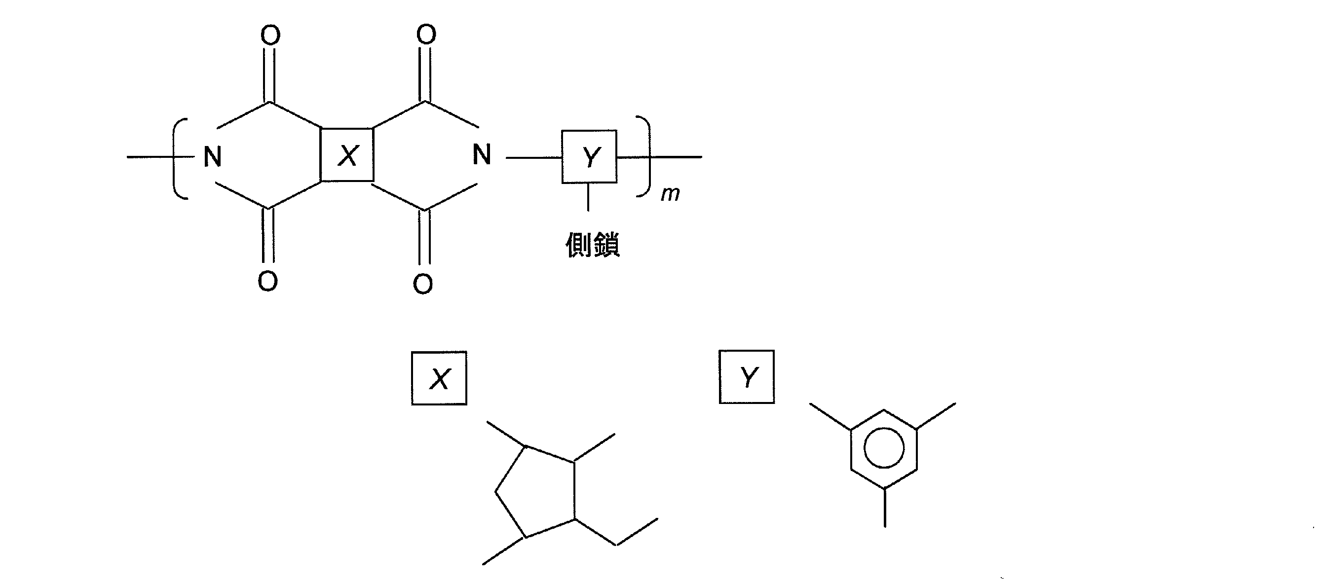

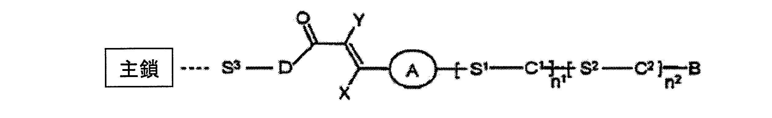
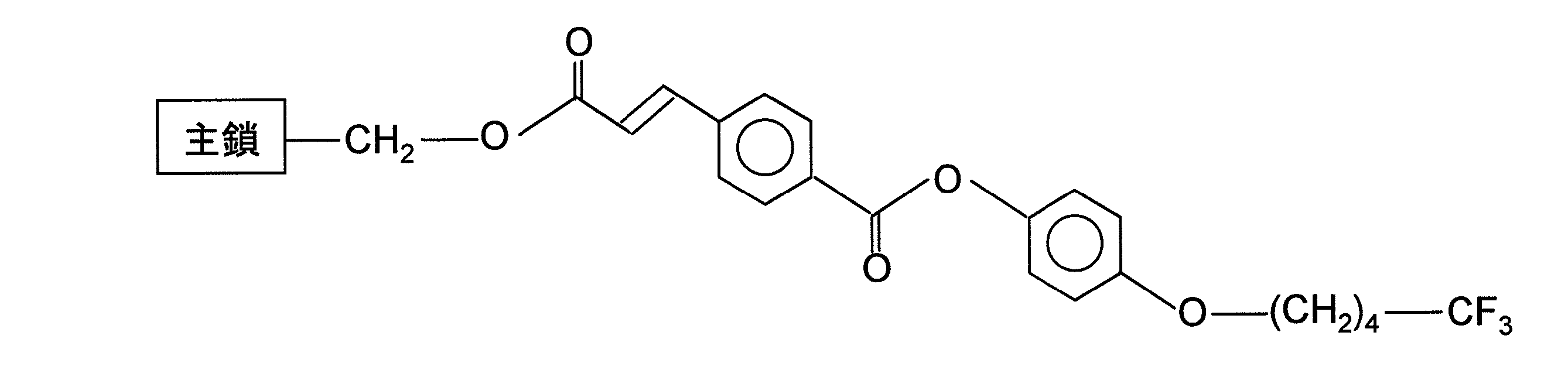


図8に、比較例1の液晶表示装置500における液晶パネル510の断面の一部の模式図を示す。
図10に、比較例2の液晶表示装置600における液晶パネル610の断面の一部の模式図を示す。
110 液晶パネル
120 アクティブマトリクス基板
122 第1透明基板
126 画素電極
128 第1配向膜
130 第1配向維持層
132 重合体
140 対向基板
146 対向電極
148 第2配向膜
150 第2配向維持層
152 重合体
160 液晶層
162 液晶分子
Claims (18)
- アクティブマトリクス基板と、対向基板と、前記アクティブマトリクス基板と前記対向基板との間に設けられた垂直配向型の液晶層とを備える液晶表示装置であって、
前記アクティブマトリクス基板および前記対向基板の少なくとも一方は光配向膜を有しており、
前記光配向膜と前記液晶層との間に設けられた配向維持層であって、光重合性化合物の重合した重合体を含む配向維持層をさらに備える、液晶表示装置。 - 前記光配向膜は、主鎖と、シンナメート基を含む側鎖とを有する高分子を含む、請求項1に記載の液晶表示装置。
- 前記液晶表示装置は複数の画素を有しており、
前記液晶層は、前記複数の画素のそれぞれに、基準配向方位の互いに異なる複数の液晶ドメインを有している、請求項1または2に記載の液晶表示装置。 - 前記アクティブマトリクス基板および前記対向基板のそれぞれが前記光配向膜を有しており、前記複数の液晶ドメインは4つの液晶ドメインである、請求項3に記載の液晶表示装置。
- 前記液晶層の液晶分子のプレチルト角は85°から89.7°の範囲内にある、請求項1から4のいずれかに記載の液晶表示装置。
- 前記光重合性化合物は、1つ以上の環構造または縮環構造と、前記環構造または縮環構造と化学結合された1つ以上の重合性官能基とを有している、請求項1から5のいずれかに記載の液晶表示装置。
- 前記光重合性化合物は重合性モノマーであり、
前記重合性モノマーは、一般式P1-A1-(Z1-A2)n-P2(P1およびP2は、それぞれ独立に、アクリレート、メタクリレート、アクリルアミド、メタクリルアミド、ビニル、ビニロキシまたはエポキシ基であり、A1およびA2は、それぞれ独立に、1,4-フェニレンまたはナフタレン-2,6-ジイル基を表し、Z1は-COO-もしくは-OCO-基または単結合であり、nは0、1または2である)で表される、請求項1から6のいずれかに記載の液晶表示装置。 - P1およびP2がアクリレート基であり、Z1が単結合であり、nが0または1である、請求項7に記載の液晶表示装置。
- P1およびP2がメタクリレート基であり、Z1が単結合であり、nが0または1である、請求項7に記載の液晶表示装置。
- P1およびP2がアクリルアミド基であり、Z1が単結合であり、nが0または1である、請求項7に記載の液晶表示装置。
- P1およびP2がメタクリルアミド基であり、Z1が単結合であり、nが0または1である、請求項7に記載の液晶表示装置。
- アクティブマトリクス基板および対向基板を用意する工程であって、光を照射して、前記アクティブマトリクス基板および前記対向基板の少なくとも一方に光配向膜を形成する工程と、
前記アクティブマトリクス基板と前記対向基板との間に、光重合性化合物を混合した液晶材料を付与することにより、前記アクティブマトリクス基板と前記対向基板との間に液晶層を形成する工程であって、電圧無印加時に、前記光配向膜により、前記液晶層の液晶分子が前記光配向膜の主面の法線方向から傾いて配向するように前記液晶分子を規定する工程と、
光を照射して前記光重合性化合物を重合させることにより、前記光配向膜と前記液晶層との間に配向維持層を形成する工程と
を包含する、液晶表示装置の製造方法。 - 前記光配向膜を形成する工程において、前記光配向膜は、主鎖と、シンナメート基を含む側鎖とを有する高分子を含む、請求項12に記載の液晶表示装置の製造方法。
- 前記配向維持層を形成する工程において、前記液晶層に電圧を印加することなく前記光の照射を行う、請求項12または13に記載の液晶表示装置の製造方法。
- 前記光配向膜を形成する工程において、前記光の波長は250nmから400nmの範囲内である、請求項12から14のいずれかに記載の液晶表示装置の製造方法。
- 前記光配向膜を形成する工程において、前記アクティブマトリクス基板および前記対向基板の少なくとも一方の主面の法線方向に対して5°以上85°以下の傾斜した方向から光を照射する、請求項12から15のいずれかに記載の液晶表示装置の製造方法。
- 前記光配向膜を形成する工程において、前記光は非偏光である、請求項12から16のいずれかに記載の液晶表示装置の製造方法。
- 前記光配向膜を形成する工程において、前記光は直線偏光、楕円偏光または円偏光である、請求項12から16のいずれかに記載の液晶表示装置の製造方法。
Priority Applications (4)
| Application Number | Priority Date | Filing Date | Title |
|---|---|---|---|
| EP09769917A EP2306238A4 (en) | 2008-06-27 | 2009-06-26 | LIQUID CRYSTAL DISPLAY DEVICE AND METHOD FOR MANUFACTURING THE SAME |
| JP2010517769A JP5357153B2 (ja) | 2008-06-27 | 2009-06-26 | 液晶表示装置およびその製造方法 |
| US13/001,537 US20110102720A1 (en) | 2008-06-27 | 2009-06-26 | Liquid crystal display device and manufacturing method therefor |
| CN2009801246167A CN102077134B (zh) | 2008-06-27 | 2009-06-26 | 液晶显示装置及其制造方法 |
Applications Claiming Priority (2)
| Application Number | Priority Date | Filing Date | Title |
|---|---|---|---|
| JP2008169036 | 2008-06-27 | ||
| JP2008-169036 | 2008-06-27 |
Publications (1)
| Publication Number | Publication Date |
|---|---|
| WO2009157207A1 true WO2009157207A1 (ja) | 2009-12-30 |
Family
ID=41444279
Family Applications (1)
| Application Number | Title | Priority Date | Filing Date |
|---|---|---|---|
| PCT/JP2009/002934 WO2009157207A1 (ja) | 2008-06-27 | 2009-06-26 | 液晶表示装置およびその製造方法 |
Country Status (6)
| Country | Link |
|---|---|
| US (1) | US20110102720A1 (ja) |
| EP (1) | EP2306238A4 (ja) |
| JP (1) | JP5357153B2 (ja) |
| KR (1) | KR20100123760A (ja) |
| CN (1) | CN102077134B (ja) |
| WO (1) | WO2009157207A1 (ja) |
Cited By (10)
| Publication number | Priority date | Publication date | Assignee | Title |
|---|---|---|---|---|
| JP2011186049A (ja) * | 2010-03-05 | 2011-09-22 | Jsr Corp | 液晶表示素子の製造方法 |
| JP2012042923A (ja) * | 2010-07-21 | 2012-03-01 | Jsr Corp | 液晶表示素子の製造方法 |
| CN102419495A (zh) * | 2010-09-27 | 2012-04-18 | 斯坦雷电气株式会社 | 液晶显示装置 |
| WO2013137254A1 (ja) * | 2012-03-13 | 2013-09-19 | シャープ株式会社 | 液晶表示装置 |
| WO2013161925A1 (ja) * | 2012-04-27 | 2013-10-31 | シャープ株式会社 | 液晶表示装置及びその製造方法 |
| WO2014061754A1 (ja) * | 2012-10-19 | 2014-04-24 | シャープ株式会社 | 液晶表示装置 |
| WO2014061756A1 (ja) * | 2012-10-19 | 2014-04-24 | シャープ株式会社 | モノマー、液晶組成物、液晶表示装置及び液晶表示装置の製造方法 |
| WO2017057496A1 (ja) * | 2015-09-30 | 2017-04-06 | 日産化学工業株式会社 | 液晶表示素子 |
| WO2018097093A1 (ja) * | 2016-11-28 | 2018-05-31 | Jnc株式会社 | 配向膜を有しない液晶表示素子の製造方法 |
| KR102708809B1 (ko) * | 2015-09-30 | 2024-09-23 | 닛산 가가쿠 가부시키가이샤 | 액정 표시 소자 |
Families Citing this family (21)
| Publication number | Priority date | Publication date | Assignee | Title |
|---|---|---|---|---|
| CN102138099B (zh) * | 2008-09-03 | 2014-09-03 | 夏普株式会社 | 取向膜、取向膜材料和具有取向膜的液晶显示装置及其制造方法 |
| JP5198580B2 (ja) | 2008-11-27 | 2013-05-15 | シャープ株式会社 | 配向膜および配向膜を有する液晶表示装置ならびに配向膜の形成方法 |
| JPWO2010116565A1 (ja) * | 2009-04-08 | 2012-10-18 | シャープ株式会社 | 液晶表示装置、液晶表示装置の製造方法、光重合体膜形成用組成物、及び、液晶層形成用組成物 |
| JP5845196B2 (ja) * | 2011-02-02 | 2016-01-20 | 東洋合成工業株式会社 | 2,2−ジメトキシ−1,2−ジ−[4−(メタ)アクリロイルオキシ]フェニルエタン−1−オン、その製造方法及びラジカル重合開始剤並びに光硬化性組成物 |
| CN102650759B (zh) * | 2012-01-06 | 2014-11-05 | 京东方科技集团股份有限公司 | 一种液晶面板及其制造方法 |
| WO2013115130A1 (ja) | 2012-01-30 | 2013-08-08 | シャープ株式会社 | 液晶表示装置およびその製造方法 |
| US20140152922A1 (en) * | 2012-12-05 | 2014-06-05 | Samsung Display Co., Ltd. | Liquid crystal display and method of manufacturing the same |
| CN103412438B (zh) * | 2013-07-31 | 2016-03-02 | 京东方科技集团股份有限公司 | 显示基板及其制备方法、双稳态液晶显示面板 |
| WO2015019616A1 (en) | 2013-08-07 | 2015-02-12 | Toyo Gosei Co., Ltd. | Reagent for enhancing generation of chemical species |
| WO2015060358A1 (ja) * | 2013-10-23 | 2015-04-30 | 日産化学工業株式会社 | 液晶配向剤、液晶配向膜及び液晶表示素子 |
| KR102205527B1 (ko) | 2014-07-18 | 2021-01-20 | 삼성디스플레이 주식회사 | 액정 표시 장치 및 그 제조 방법 |
| CN105116621A (zh) * | 2015-09-01 | 2015-12-02 | 深圳市华星光电技术有限公司 | 液晶面板的制造方法 |
| CN105137660A (zh) * | 2015-09-25 | 2015-12-09 | 京东方科技集团股份有限公司 | 一种光配向膜杂质去除装置和方法 |
| KR102621126B1 (ko) * | 2015-12-30 | 2024-01-03 | 엘지디스플레이 주식회사 | 액정 표시 장치 |
| US11078324B2 (en) * | 2016-10-28 | 2021-08-03 | Sharp Kabushiki Kaisha | Seal material composition, liquid crystal cell, and scanned antenna |
| CN206602182U (zh) * | 2017-04-06 | 2017-10-31 | 京东方科技集团股份有限公司 | 一种天线结构及通讯设备 |
| KR102456697B1 (ko) * | 2017-08-22 | 2022-10-19 | 삼성디스플레이 주식회사 | 액정 표시 장치 및 이의 제조 방법 |
| CN107357089B (zh) * | 2017-09-07 | 2020-08-28 | 深圳市华星光电技术有限公司 | 液晶显示面板及光配向方法 |
| CN112445029A (zh) * | 2019-09-05 | 2021-03-05 | 咸阳彩虹光电科技有限公司 | 一种液晶显示面板及显示器 |
| CN112882291A (zh) * | 2021-01-18 | 2021-06-01 | 深圳市华星光电半导体显示技术有限公司 | 液晶材料的光配向方法 |
| JP2022154781A (ja) * | 2021-03-30 | 2022-10-13 | 株式会社ジャパンディスプレイ | 配向膜材料、及び、液晶表示装置 |
Citations (9)
| Publication number | Priority date | Publication date | Assignee | Title |
|---|---|---|---|---|
| JPH11352486A (ja) | 1998-06-08 | 1999-12-24 | Sharp Corp | 液晶電気光学装置 |
| JP2000122066A (ja) * | 1998-10-21 | 2000-04-28 | Hitachi Ltd | 液晶表示装置 |
| JP2002357830A (ja) | 2001-03-30 | 2002-12-13 | Fujitsu Ltd | 液晶表示装置 |
| JP2003149647A (ja) | 2001-08-31 | 2003-05-21 | Fujitsu Display Technologies Corp | 液晶表示装置及びその製造方法 |
| JP2003520878A (ja) * | 2000-01-24 | 2003-07-08 | ロリク アーゲー | 側鎖の光架橋性基を有する光活性ポリイミド、ポリアミド酸又はエステル |
| JP3520376B2 (ja) | 1993-06-11 | 2004-04-19 | セイコーエプソン株式会社 | 液晶表示素子およびその製造方法 |
| JP2006215184A (ja) * | 2005-02-02 | 2006-08-17 | Jsr Corp | 液晶配向膜および液晶表示素子とその製造法 |
| JP2007322274A (ja) | 2006-06-01 | 2007-12-13 | Mitsubishi Electric Corp | 侵入物体識別装置 |
| JP2008076950A (ja) * | 2006-09-25 | 2008-04-03 | Sharp Corp | 液晶表示パネル及びその製造方法 |
Family Cites Families (8)
| Publication number | Priority date | Publication date | Assignee | Title |
|---|---|---|---|---|
| EP1219651A1 (en) * | 2000-12-29 | 2002-07-03 | Rolic AG | Photoactive copolymer |
| EP1277770A1 (en) * | 2001-07-17 | 2003-01-22 | Rolic AG | Photoactive materials |
| US6952252B2 (en) * | 2001-10-02 | 2005-10-04 | Fujitsu Display Technologies Corporation | Substrate for liquid crystal display and liquid crystal display utilizing the same |
| US6919404B2 (en) * | 2002-05-31 | 2005-07-19 | Elsicon, Inc. | Hybrid polymer materials for liquid crystal alignment layers |
| EP1720163A1 (en) * | 2005-05-05 | 2006-11-08 | Fraunhofer-Gesellschaft Zur Förderung Der Angewandten Forschung E.V. | Film forming photosensitive materials for the light induced generation of optical anisotropy |
| CN102138099B (zh) * | 2008-09-03 | 2014-09-03 | 夏普株式会社 | 取向膜、取向膜材料和具有取向膜的液晶显示装置及其制造方法 |
| JP5198580B2 (ja) * | 2008-11-27 | 2013-05-15 | シャープ株式会社 | 配向膜および配向膜を有する液晶表示装置ならびに配向膜の形成方法 |
| RU2011143816A (ru) * | 2009-03-30 | 2013-05-10 | Шарп Кабусики Кайся | Жидкокристаллическое дисплейное устройство, способ получения жидкокристаллического дисплейного устройства, композиция для получения полимерного слоя и композиция для получения жидкокристаллического слоя |
-
2009
- 2009-06-26 EP EP09769917A patent/EP2306238A4/en not_active Withdrawn
- 2009-06-26 JP JP2010517769A patent/JP5357153B2/ja not_active Expired - Fee Related
- 2009-06-26 CN CN2009801246167A patent/CN102077134B/zh not_active Expired - Fee Related
- 2009-06-26 KR KR1020107022691A patent/KR20100123760A/ko active IP Right Grant
- 2009-06-26 WO PCT/JP2009/002934 patent/WO2009157207A1/ja active Application Filing
- 2009-06-26 US US13/001,537 patent/US20110102720A1/en not_active Abandoned
Patent Citations (9)
| Publication number | Priority date | Publication date | Assignee | Title |
|---|---|---|---|---|
| JP3520376B2 (ja) | 1993-06-11 | 2004-04-19 | セイコーエプソン株式会社 | 液晶表示素子およびその製造方法 |
| JPH11352486A (ja) | 1998-06-08 | 1999-12-24 | Sharp Corp | 液晶電気光学装置 |
| JP2000122066A (ja) * | 1998-10-21 | 2000-04-28 | Hitachi Ltd | 液晶表示装置 |
| JP2003520878A (ja) * | 2000-01-24 | 2003-07-08 | ロリク アーゲー | 側鎖の光架橋性基を有する光活性ポリイミド、ポリアミド酸又はエステル |
| JP2002357830A (ja) | 2001-03-30 | 2002-12-13 | Fujitsu Ltd | 液晶表示装置 |
| JP2003149647A (ja) | 2001-08-31 | 2003-05-21 | Fujitsu Display Technologies Corp | 液晶表示装置及びその製造方法 |
| JP2006215184A (ja) * | 2005-02-02 | 2006-08-17 | Jsr Corp | 液晶配向膜および液晶表示素子とその製造法 |
| JP2007322274A (ja) | 2006-06-01 | 2007-12-13 | Mitsubishi Electric Corp | 侵入物体識別装置 |
| JP2008076950A (ja) * | 2006-09-25 | 2008-04-03 | Sharp Corp | 液晶表示パネル及びその製造方法 |
Non-Patent Citations (1)
| Title |
|---|
| See also references of EP2306238A4 * |
Cited By (16)
| Publication number | Priority date | Publication date | Assignee | Title |
|---|---|---|---|---|
| JP2011186049A (ja) * | 2010-03-05 | 2011-09-22 | Jsr Corp | 液晶表示素子の製造方法 |
| JP2012042923A (ja) * | 2010-07-21 | 2012-03-01 | Jsr Corp | 液晶表示素子の製造方法 |
| KR101809987B1 (ko) * | 2010-07-21 | 2017-12-18 | 제이에스알 가부시끼가이샤 | 액정 표시 소자 및 그의 제조 방법 |
| CN102419495A (zh) * | 2010-09-27 | 2012-04-18 | 斯坦雷电气株式会社 | 液晶显示装置 |
| US9235083B2 (en) | 2012-03-13 | 2016-01-12 | Sharp Kabushiki Kaisha | Liquid crystal display device |
| WO2013137254A1 (ja) * | 2012-03-13 | 2013-09-19 | シャープ株式会社 | 液晶表示装置 |
| WO2013161925A1 (ja) * | 2012-04-27 | 2013-10-31 | シャープ株式会社 | 液晶表示装置及びその製造方法 |
| JPWO2014061756A1 (ja) * | 2012-10-19 | 2016-09-05 | シャープ株式会社 | モノマー、液晶組成物、液晶表示装置及び液晶表示装置の製造方法 |
| WO2014061756A1 (ja) * | 2012-10-19 | 2014-04-24 | シャープ株式会社 | モノマー、液晶組成物、液晶表示装置及び液晶表示装置の製造方法 |
| WO2014061754A1 (ja) * | 2012-10-19 | 2014-04-24 | シャープ株式会社 | 液晶表示装置 |
| US9983441B2 (en) | 2012-10-19 | 2018-05-29 | Merck Patent Gmbh | Liquid crystal display device |
| US10059881B2 (en) | 2012-10-19 | 2018-08-28 | Sharp Kabushiki Kaisha | Monomer, liquid crystal composition, liquid crystal display device, and production method for liquid crystal display device |
| WO2017057496A1 (ja) * | 2015-09-30 | 2017-04-06 | 日産化学工業株式会社 | 液晶表示素子 |
| US11112654B2 (en) | 2015-09-30 | 2021-09-07 | Nissan Chemical Industries, Ltd. | Liquid crystal display device |
| KR102708809B1 (ko) * | 2015-09-30 | 2024-09-23 | 닛산 가가쿠 가부시키가이샤 | 액정 표시 소자 |
| WO2018097093A1 (ja) * | 2016-11-28 | 2018-05-31 | Jnc株式会社 | 配向膜を有しない液晶表示素子の製造方法 |
Also Published As
| Publication number | Publication date |
|---|---|
| JP5357153B2 (ja) | 2013-12-04 |
| EP2306238A4 (en) | 2012-09-12 |
| EP2306238A1 (en) | 2011-04-06 |
| JPWO2009157207A1 (ja) | 2011-12-08 |
| KR20100123760A (ko) | 2010-11-24 |
| CN102077134A (zh) | 2011-05-25 |
| US20110102720A1 (en) | 2011-05-05 |
| CN102077134B (zh) | 2013-11-27 |
Similar Documents
| Publication | Publication Date | Title |
|---|---|---|
| JP5357153B2 (ja) | 液晶表示装置およびその製造方法 | |
| JP5198577B2 (ja) | 配向膜、配向膜材料および配向膜を有する液晶表示装置ならびにその形成方法 | |
| JP5198580B2 (ja) | 配向膜および配向膜を有する液晶表示装置ならびに配向膜の形成方法 | |
| JP5357163B2 (ja) | 配向膜、配向膜材料および配向膜を有する液晶表示装置ならびにその製造方法 | |
| JP5296096B2 (ja) | 液晶表示装置及びその製造方法 | |
| US20130271713A1 (en) | Liquid crystal display device and method for manufacturing liquid crystal display device | |
| WO2010079703A1 (ja) | 液晶表示装置及び液晶層形成用組成物 | |
| WO2012050178A1 (ja) | 液晶表示装置 | |
| WO2010116565A1 (ja) | 液晶表示装置、液晶表示装置の製造方法、光重合体膜形成用組成物、及び、液晶層形成用組成物 | |
| TWI519868B (zh) | Liquid crystal display device | |
| WO2010106915A1 (ja) | 液晶表示装置及びその製造方法 | |
| WO2012086715A1 (ja) | 液晶配向剤、液晶表示装置、及び、液晶表示装置の製造方法 | |
| WO2012014803A1 (ja) | 液晶表示装置およびその製造方法 | |
| US10527890B2 (en) | Liquid crystal display and manufacturing method thereof | |
| WO2014045923A1 (ja) | 液晶表示装置及びその製造方法 | |
| US20130342798A1 (en) | Liquid crystal display panel, liquid crystal display apparatus, and liquid crystal display cell | |
| US10684513B2 (en) | Liquid crystal display and production method therefor | |
| JP2015206806A (ja) | 液晶表示装置及びその製造方法 | |
| WO2014061754A1 (ja) | 液晶表示装置 | |
| WO2013031497A1 (ja) | 液晶表示装置、及び、液晶組成物 |
Legal Events
| Date | Code | Title | Description |
|---|---|---|---|
| WWE | Wipo information: entry into national phase |
Ref document number: 200980124616.7 Country of ref document: CN |
|
| 121 | Ep: the epo has been informed by wipo that ep was designated in this application |
Ref document number: 09769917 Country of ref document: EP Kind code of ref document: A1 |
|
| ENP | Entry into the national phase |
Ref document number: 20107022691 Country of ref document: KR Kind code of ref document: A |
|
| WWE | Wipo information: entry into national phase |
Ref document number: 2010517769 Country of ref document: JP |
|
| WWE | Wipo information: entry into national phase |
Ref document number: 13001537 Country of ref document: US |
|
| NENP | Non-entry into the national phase |
Ref country code: DE |
|
| WWE | Wipo information: entry into national phase |
Ref document number: 2009769917 Country of ref document: EP |