WO2009130946A1 - 保護素子及びその製造方法 - Google Patents
保護素子及びその製造方法 Download PDFInfo
- Publication number
- WO2009130946A1 WO2009130946A1 PCT/JP2009/053870 JP2009053870W WO2009130946A1 WO 2009130946 A1 WO2009130946 A1 WO 2009130946A1 JP 2009053870 W JP2009053870 W JP 2009053870W WO 2009130946 A1 WO2009130946 A1 WO 2009130946A1
- Authority
- WO
- WIPO (PCT)
- Prior art keywords
- solder
- elastic member
- electrode terminals
- protective element
- heating resistor
- Prior art date
- Legal status (The legal status is an assumption and is not a legal conclusion. Google has not performed a legal analysis and makes no representation as to the accuracy of the status listed.)
- Ceased
Links
Images




Classifications
-
- H—ELECTRICITY
- H01—ELECTRIC ELEMENTS
- H01H—ELECTRIC SWITCHES; RELAYS; SELECTORS; EMERGENCY PROTECTIVE DEVICES
- H01H85/00—Protective devices in which the current flows through a part of fusible material and this current is interrupted by displacement of the fusible material when this current becomes excessive
- H01H85/02—Details
- H01H85/36—Means for applying mechanical tension to fusible member
-
- H—ELECTRICITY
- H01—ELECTRIC ELEMENTS
- H01H—ELECTRIC SWITCHES; RELAYS; SELECTORS; EMERGENCY PROTECTIVE DEVICES
- H01H83/00—Protective switches, e.g. circuit-breaking switches, or protective relays operated by abnormal electrical conditions otherwise than solely by excess current
- H01H83/20—Protective switches, e.g. circuit-breaking switches, or protective relays operated by abnormal electrical conditions otherwise than solely by excess current operated by excess current as well as by some other abnormal electrical condition
-
- H—ELECTRICITY
- H01—ELECTRIC ELEMENTS
- H01H—ELECTRIC SWITCHES; RELAYS; SELECTORS; EMERGENCY PROTECTIVE DEVICES
- H01H37/00—Thermally-actuated switches
- H01H37/74—Switches in which only the opening movement or only the closing movement of a contact is effected by heating or cooling
- H01H37/76—Contact member actuated by melting of fusible material, actuated due to burning of combustible material or due to explosion of explosive material
- H01H37/761—Contact member actuated by melting of fusible material, actuated due to burning of combustible material or due to explosion of explosive material with a fusible element forming part of the switched circuit
- H01H2037/762—Contact member actuated by melting of fusible material, actuated due to burning of combustible material or due to explosion of explosive material with a fusible element forming part of the switched circuit using a spring for opening the circuit when the fusible element melts
-
- H—ELECTRICITY
- H01—ELECTRIC ELEMENTS
- H01H—ELECTRIC SWITCHES; RELAYS; SELECTORS; EMERGENCY PROTECTIVE DEVICES
- H01H85/00—Protective devices in which the current flows through a part of fusible material and this current is interrupted by displacement of the fusible material when this current becomes excessive
- H01H85/02—Details
- H01H85/04—Fuses, i.e. expendable parts of the protective device, e.g. cartridges
- H01H85/041—Fuses, i.e. expendable parts of the protective device, e.g. cartridges characterised by the type
- H01H85/0411—Miniature fuses
- H01H2085/0414—Surface mounted fuses
-
- H—ELECTRICITY
- H01—ELECTRIC ELEMENTS
- H01H—ELECTRIC SWITCHES; RELAYS; SELECTORS; EMERGENCY PROTECTIVE DEVICES
- H01H85/00—Protective devices in which the current flows through a part of fusible material and this current is interrupted by displacement of the fusible material when this current becomes excessive
- H01H85/02—Details
- H01H85/46—Circuit arrangements not adapted to a particular application of the protective device
- H01H2085/466—Circuit arrangements not adapted to a particular application of the protective device with remote controlled forced fusing
-
- H—ELECTRICITY
- H01—ELECTRIC ELEMENTS
- H01H—ELECTRIC SWITCHES; RELAYS; SELECTORS; EMERGENCY PROTECTIVE DEVICES
- H01H83/00—Protective switches, e.g. circuit-breaking switches, or protective relays operated by abnormal electrical conditions otherwise than solely by excess current
- H01H83/10—Protective switches, e.g. circuit-breaking switches, or protective relays operated by abnormal electrical conditions otherwise than solely by excess current operated by excess voltage, e.g. for lightning protection
-
- H—ELECTRICITY
- H01—ELECTRIC ELEMENTS
- H01H—ELECTRIC SWITCHES; RELAYS; SELECTORS; EMERGENCY PROTECTIVE DEVICES
- H01H85/00—Protective devices in which the current flows through a part of fusible material and this current is interrupted by displacement of the fusible material when this current becomes excessive
- H01H85/02—Details
- H01H85/46—Circuit arrangements not adapted to a particular application of the protective device
-
- Y—GENERAL TAGGING OF NEW TECHNOLOGICAL DEVELOPMENTS; GENERAL TAGGING OF CROSS-SECTIONAL TECHNOLOGIES SPANNING OVER SEVERAL SECTIONS OF THE IPC; TECHNICAL SUBJECTS COVERED BY FORMER USPC CROSS-REFERENCE ART COLLECTIONS [XRACs] AND DIGESTS
- Y10—TECHNICAL SUBJECTS COVERED BY FORMER USPC
- Y10T—TECHNICAL SUBJECTS COVERED BY FORMER US CLASSIFICATION
- Y10T29/00—Metal working
- Y10T29/49—Method of mechanical manufacture
- Y10T29/49002—Electrical device making
- Y10T29/49105—Switch making
Definitions
- the present invention relates to a protective element that cuts off a current when a device to be protected is abnormal and a method for manufacturing the same.
- a chip-shaped protective element in which a low melting point metal body (fuse element) is provided on a substrate is known.
- the fuse element melts due to an overcurrent flowing through the fuse element in the event of an abnormality.
- the melted fuse element is drawn onto the electrode due to the good wettability with respect to the electrode surface on which the fuse element is placed. As a result, in the protection element, the fuse element is blown and the current is interrupted.
- a protective element that can be used to prevent not only overcurrent but also overvoltage
- a chip-shaped protective element in which a heating resistor and a fuse element are stacked on a substrate is also known.
- the heat generating resistor is energized in the event of an abnormality, and the heat generating resistor generates heat, thereby melting the fuse element.
- the melted fuse element is drawn onto the electrode due to the good wettability with respect to the electrode surface on which the fuse element is placed. As a result, in the protection element, the fuse element is blown and the current is interrupted.
- Such protection elements are usually mounted on the base circuit board of the protection target device by reflow mounting. Therefore, in order to prevent the fuse element from being melted when the protection element is mounted on the base circuit board, a material having a solid phase point higher than the mounting temperature is used.
- a protection element mounting method has been proposed in which the mounting temperature is lower than the liquidus point of the fuse element and higher than the solidus point (see, for example, Patent Document 1).
- JP 2004-363630 A JP-A-9-306319 Japanese Utility Model Publication No. 53-42145
- solder paste used for reflow mounting of protective elements but also solder foil as a fuse element is required to be lead-free.
- the reflow temperature is increased to about 260 ° C. with the lead-free solder, and in order to prevent the fuse element from being blown when the protective element is mounted on the base circuit board, it is 260 ° C. or higher.
- the lead-free solder that has a liquid phase point or a solid phase point and is practical as a fuse element has not yet been found.
- Lead-free solder that is practical as a fuse element means that the solder foil melts at a temperature of 260 ° C or higher, and the surface is tensioned to minimize the surface area. It has the characteristic to do.
- the present invention has been made in view of such circumstances, and can be applied to reflow mounting, and is good even if the liquid phase point or solid phase point of the solder used is higher than the mounting temperature. It is an object of the present invention to provide a protective element capable of obtaining the response of the current interruption operation and a manufacturing method thereof.
- the inventor of the present application considered the fact that no lead-free solder replacing the existing solder material has been found so far, and considered cutting off the current without providing a fuse element.
- the inventor of the present application has found a novel configuration capable of obtaining good current interruption operation response even when the liquid phase point or solid phase point of the solder used is higher than the mounting temperature. It came to complete.
- the protection element according to the present invention that achieves the above-described object is provided on a predetermined substrate so that a current interrupting portion is divided into a plurality of current paths in a protection element that interrupts current when a protection target device is abnormal.
- An elastic member is fixed to a plurality of formed electrode terminals via solder, and the solder has a liquidus point higher than the mounting temperature when the protection element is mounted on the protection target device. The elastic member is deformed even in a state where the solder is not completely melted, so that the elastic member retains the stress to the extent that it is separated from at least one of the plurality of electrode terminals. It is characterized by being attached.
- Such a protection element according to the present invention is configured by using an elastic member as a connection member of the current interrupting portion and fixing it to the electrode terminal with solder.
- the protective element according to the present invention maintains the stress to the extent that it separates from at least one of the plurality of electrode terminals by deforming even when the solder is not completely melted. Therefore, it is not necessary to completely melt the solder in order to cut off the current.
- the elastic member is physically separated from the electrode terminal by the stress of the elastic member, and the current is Blocking can be performed.
- a method for manufacturing a protection element according to the present invention is a method for manufacturing a protection element that cuts off a current when a device to be protected is abnormal.
- a first step of applying solder having a liquidus point higher than a mounting temperature when mounting the protection element on the protection target device on a plurality of electrode terminals formed on a predetermined substrate; and the solder A second step of mounting a predetermined elastic member so as to straddle over the plurality of electrode terminals coated with, and melting the solder by heating in a state where the elastic member is bent and brought into contact with the solder And a third step of fixing to the plurality of electrode terminals in a state where the elastic member is urged, and in the third step, the solder is deformed even when the solder is not completely melted.
- the plurality of electrode terminals by Of while maintaining the degree of stress away from the at least one electrode terminal, it is characterized by soldering the elastic member to the plurality of electrode terminals.
- the manufacturing method of the protection element according to the present invention is a method of manufacturing a protection element that cuts off a current when a protection target device is abnormal.
- a first step of applying solder having a liquidus point higher than a mounting temperature when mounting the protection element on the protection target device on a plurality of electrode terminals formed on a predetermined substrate; and the solder A second step of mounting a predetermined elastic member so as to straddle over the plurality of electrode terminals coated with, and heating the state in which the elastic member is mounted to melt the solder, and then cooling the
- the third step In the third step, In the state that the solder does not melt completely By deforming while holding the degree of stress away from at least one of electrode terminals of the plurality of electrode terminals it is characterized by soldering the elastic member to the plurality of electrode terminals.
- a protection element configured by using an elastic member as a connection member of the current interrupting portion and fixing it to the electrode terminal with solder can be easily manufactured.
- the protective element manufactured in this way is in a state in which the plurality of electrodes are maintained in a state in which the stress is maintained to be separated from at least one of the plurality of electrode terminals by being deformed even when the solder is not completely melted. Since it is soldered to the terminal, it is not necessary to completely melt the solder in order to cut off the current, and the elastic member is physically separated from the electrode terminal by the stress of the elastic member when the solder is melted to some extent, Current interruption can be performed.
- the present invention it is not necessary to completely melt the solder in order to cut off the current, and when the solder is melted to some extent, the solder is physically separated from the electrode terminal by the stress of the elastic member. Since the elastic member is connected to the electrode terminal of the current interrupting unit, the response of the current interrupting operation can be obtained even if the liquid phase point or solid phase point of the solder used is higher than the mounting temperature. It can be applied to reflow mounting.
- This embodiment is a protective element that is connected in series to the energization path of the device to be protected and cuts off the current when the device to be protected is abnormal.
- this protective element uses an elastic member instead of a fuse element as a connecting member for the current interrupting part, and connects or disconnects the elastic member to the current-carrying electrode terminal of the current interrupting part using solder, thereby preventing current from being supplied or interrupted. It can be controlled.
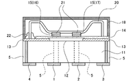
- the protection element is a heating resistor 12 that generates heat when energized when a protection target device is abnormal on a substrate 11 having a predetermined size. And a first conductor layer 13 electrically connected to the heating resistor 12 is formed.
- the substrate 11 may be any circuit substrate made of an insulating material, for example, a substrate used for a printed wiring board such as a ceramic substrate or a glass epoxy substrate, a glass substrate, a resin substrate. Insulating metal substrates can be used. Among these, a ceramic substrate which is an insulating substrate having excellent heat resistance and heat conductivity is suitable.
- a heating resistor terminal 3 for generating heat from the heating resistor 12, and the protection element as a base of the device to be protected.
- NC (Non-Connection) terminals 4 for mounting on the circuit board are formed. Further, on the side surface of the substrate 11, a side conductor layer 5 electrically connected to each of the energization path terminals 1, 2, the heating resistor terminal 3, and the mounting NC terminal 4 is formed.
- the heating resistor 12 is formed by, for example, applying a resistance paste made of a conductive material such as ruthenium oxide and an inorganic binder such as water glass or an organic binder such as a thermosetting resin, and firing it as necessary. It is formed. Further, as the heating resistor 12, a thin film such as ruthenium oxide or carbon black may be formed through printing, plating, vapor deposition, sputtering, or may be formed by pasting or laminating these films.
- the heating resistor 12 has a side conductor layer 5 and a first conductor layer 13 connected to the heating resistor terminal 3 as the potential of the heating resistor terminal 3 decreases when the device to be protected is abnormal. It generates heat when it is energized through.
- the first conductor layer 13 forms a heating resistor electrode terminal for energizing the heating resistor 12.
- the constituent material of this 1st conductor layer 13 Since the said 1st conductor layer 13 forms an electricity supply path
- the first conductor layer 13 may be made of Ag, Ag—Pt, Ag—Pd, or the like, or may be formed by applying gold plating to the surface.
- the second conductor layer 15 is formed on the heating resistor 12 and the first conductor layer 13 via an insulating layer 14 such as glass in a direction orthogonal to the first conductor layer 13. Are formed, and two energization electrode terminals 16 and 17 for dividing the energization path into two to form a current interrupting portion are formed in parallel.
- the second conductor layer 15 and the energization electrode terminals 16 and 17 form an energization path together with the first conductor layer 13.
- the second conductor layer 15 is also a current-carrying electrode terminal similarly to the current-carrying electrode terminals 16 and 17 and is provided in order to increase resistance to a large amount of flowing current.
- the second conductor layer 15 and the energizing electrode terminals 16 and 17 are disposed in a state of being insulated from the heating resistor 12 via the insulating layer 14.
- the second conductor layer 15 and the energization electrode terminals 16 and 17 are electrode terminals provided corresponding to the energization path terminals 1 and 2, respectively, and side conductors connected to the energization path terminals 1 and 2, respectively.
- the constituent materials of the second conductor layer 15 and the energizing electrode terminals 16 and 17 are not particularly limited. However, since the second conductor layer 15 and the energizing electrode terminals 16 and 17 form an energizing path, they will be described later. It is desirable to use a solder 21 and a metal made of a metal having good wettability. In particular, the second conductor layer 15 and the energization electrode terminals 16 and 17 are usually formed by the same manufacturing process as the first conductor layer 13, and thus are formed from the same material as the first conductor layer 13. .
- the arrangement relationship between the second conductor layer 15 and the energizing electrode terminals 16 and 17 and the heating resistor 12 will be described later with respect to the second conductor layer 15 and the energizing electrode terminals 16 and 17 due to the heat generated by the heating resistor 12.
- at least directly below the second conductor layer 15 and the energizing electrode terminals 16 and 17. By providing the heating resistor 12 directly below the portion where the elastic member 20 straddles on the second conductor layer 15 and the energizing electrode terminals 16 and 17, the melting of the solder 21 described later due to the heat generated by the heating resistor 12 is accelerated. It is possible to improve the responsiveness of the current interruption operation.
- the elastic member 20 is disposed in a form fixed to the second conductor layer 15 and the energizing electrode terminals 16 and 17.
- the elastic member 20 is formed, for example, as a conductive leaf spring material having a substantially U-shape when not energized, and has two sides that connect two opposite sides of the substantially U-shape. In a state where the central portion is bent inward in a substantially U-shape and biased in a generally M-shaped shape as a whole, the central portion is soldered to the second conductor layer 15 and the energizing electrode terminals 16 and 17.
- the second conductor layer 15 and the current-carrying electrode terminals 16 and 17 are electrically connected to each other by being fixed thereto.
- the elastic member 20 has one edge located on the insulating layer 14 and the other edge located on the first conductor layer 13 as a heating resistor electrode terminal. It is electrically connected to the first conductor layer 13 by being fixed to the first conductor layer 13 via the solder 22. Thereby, the elastic member 20 forms an energization path.
- the constituent material of such an elastic member 20 Since the said elastic member 20 forms an electricity supply path
- the elastic member 20 has a relatively small electrical resistance and good wettability with the solders 21 and 22, and further has high elastic force, tensile strength, and hardness, and is excellent in wear resistance and corrosion resistance. What is formed from phosphor bronze can be used.
- the solders 21 and 22 may have the same composition or different compositions, but in any case, various low-melting-point metal bodies conventionally used can be used.
- various low-melting-point metal bodies conventionally used can be used.
- a SnSb alloy, a BiSnPb alloy, a BiPbSn alloy, a BiPb alloy, a BiSn alloy, a SnPb alloy, a SnAg alloy, a PbIn alloy, a ZnAl alloy, an InSn alloy, a PbAgSn alloy, and the like can be given.
- lead-free solders such as SnSb alloy and SnCu alloy from the viewpoint of lead-free requirements.
- solder 21 among the solders 21 and 22 that has a liquidus point higher than the mounting temperature when mounting the protection element on the protection target device.
- the solder 21 has a liquidus point of 260 ° C. or higher and 350 ° C. or lower in consideration of the heating temperature of the heating resistor 12 when the protective element is reflow mounted on the protection target device. Is desirable.
- the solder 21 does not require the property of exhibiting the cohesive force of the molten solder, that is, the surface tension, which is required for the heat fusing, like the fuse element that has been responsible for interrupting the current in the conventional protection element,
- the physical fixing force is reduced at the temperature (melting point) of the solid phase point or the liquid phase point, and the stress (biasing force) of the elastic member 20 exceeds the fixing force, so that the elastic member 20 becomes the second conductor layer. 15 and the current-carrying electrode terminals 16 and 17 are sufficient.
- the elastic member 20 deforms even in a state where the solder 21 is not completely melted, so that the elastic member 20 has a stress that is separated from at least one of the second conductive layer 15 and the conductive electrode terminals 16 and 17. What is necessary is just to be soldered to the said 2nd conductor layer 15 and the said electricity supply electrode terminals 16 and 17 in the state hold
- the amount of the solders 21 and 22 depends on the fixing area between the heating resistor electrode terminal, the second conductor layer 15 and the current-carrying electrode terminals 16 and 17, but a small amount is sufficient. About 2 mg is sufficient.
- the protective element protects and regulates the behavior range of the elastic member 20, and the protective element is used as a chip component having an automatic component mounting adsorption area for the purpose of SMT (Surface-Mount-Technology) automatic mounting.
- the elastic member 20 is covered with an insulating case 18 made of, for example, a liquid crystal polymer.
- the insulating case 18 has a cap-like hollow structure so as not to hinder the current interruption operation caused by the elastic member 20 being separated from the second conductor layer 15 and the energizing electrode terminals 16 and 17.
- the surface covered with the insulating case 18 may be provided with a surface active member made of flux or the like in order to prevent surface oxidation.
- the flux any known flux such as rosin flux can be used, and the viscosity and the like are arbitrary.
- the circuit configuration of such a protection element can be expressed as shown in FIG. That is, in the protective element, the energization path AB is constituted by at least the second conductor layer 15 and the energization electrode terminals 16 and 17 provided between the energization path terminals 1 and 2, and the elastic member 20, and the elastic member Since 20 is electrically connected to the first conductor layer 13 via the solder 22, the heating resistor 12 is energized via the energization path AB including the elastic member 20. .
- this protection element when energization is performed from the energization path AB and the heating resistor 12 generates heat, at least one energization electrode terminal and the elastic member of the second conductor layer 15 and the energization electrode terminals 16 and 17 are used. As a result, the solder 21 connecting 20 is melted.
- the resistance value of the heating resistor 12 varies depending on the potential of the energizing path AB, but for example, assuming a design in which a voltage of 12.6 V is applied to the energizing path AB, about 5 ⁇ to 10 ⁇ . Is desirable. However, this resistance value depends on various conditions such as the heat conduction characteristics of the substrate 11 and the presumed operating temperature environment, and appropriate design verification for each application is required.
- the resistance value of the energization path AB mainly composed of the elastic member 20 and the solder 21 is such that the elastic member 20 and the solder 21 are heated when a current more than twice the rated current flows through the energization path.
- such a protection element performs the following operation as a protection circuit operation including an overvoltage operation. That is, in the protection element, the potential of the heating resistor terminal 3 is set to the ground level in response to the input of a predetermined cutoff signal supplied from an external protection circuit including a switch such as a field effect transistor when the protection target device is abnormal. To drop. As a result, in the protection element, a current flows to the heating resistor 12 from the energization path having a higher potential than the ground, and accordingly, the heating resistor 12 generates heat.
- the second conductor layer 15 provided in the vicinity of the heating resistor 12 and the solder that fixes at least one energizing electrode terminal and the elastic member 20 among the energizing electrode terminals 16 and 17.
- the elastic member 20 is separated from the second conductor layer 15 and the energizing electrode terminals 16 and 17 to be in a non-energized state, thereby interrupting the energizing path.
- the heat generation of the heating resistor 12 is stopped according to the interruption of the energization path.
- the elastic member 20 and the solder 21 forming the energization path are heated when a current that is, for example, twice or more of the rated current flows through the energization path.
- the solder 21 is melted, and the elastic member 20 is separated from the second conductor layer 15 and the energization electrode terminals 16 and 17 to be in a non-energized state, thereby interrupting the energization path.
- the protective element can block the energization path according to the operation of the elastic member 20, and can prevent overcurrent and overvoltage.
- movement can be manufactured as follows.
- a substrate 11 on which a heating resistor 12, a first conductor layer 13, an insulating layer 14, a second conductor layer 15, and energizing electrode terminals 16 and 17 are formed using existing wiring board manufacturing technology is prepared. Then, the solder 21 is applied on the current-carrying electrode terminals 16 and 17 and the first conductor layer 13 where the elastic member 20 is soldered.
- the elastic member 20 having a substantially U-shape is positioned on one end edge of the elastic member 20 on the insulating layer 14 and the other end edge is positioned on the first conductor layer 13. It is positioned and mounted so as to straddle the second conductor layer 15 and the energizing electrode terminals 16 and 17.
- the central portion of the elastic member 20 is bent in a substantially U-shaped inner side and heated in contact with the solder 21 to melt the solders 21 and 22.
- the elastic member 20 is fixed to the second conductor layer 15, the current-carrying electrode terminals 16 and 17, and the first conductor layer 13 in a state where the elastic member 20 is urged in a substantially M shape.
- this heating and cooling process can be performed by inserting the prepared pre-finished element into a predetermined heating and cooling furnace, or heating and cooling the pressing jig.
- the elastic member 20 can be fixed using the heat generated by the heating resistor 12 by energizing and shutting off the heating resistor 12. . Furthermore, by using, for example, a pressing head having a plurality of protrusions, such as Kenzan, as the pressing jig, the elastic member 20 can be simultaneously mounted on each of the plurality of elements, thereby improving the yield. it can.
- a pressing head having a plurality of protrusions such as Kenzan
- the protective element can be manufactured by fixing the insulating case 18 to the pre-finished element on which the elastic member 20 is mounted in this way.
- the protective element uses the elastic member 20 as a connecting member of the current interrupting portion instead of the fuse element made of solder foil as in the prior art, and uses the solder 21 to connect the elastic member 20 to the current interrupting portion.
- the second conductor layer 15 and the energizing electrode terminals 16 and 17 lead-free can be achieved. Therefore, in this protection element, even if the liquid phase point or solid phase point of the solder 21 to be used is higher than the mounting temperature, the response of the current interruption operation is the same as that of the conventional protection element using the fuse element. Sex can be obtained.
- the stress is maintained so as to be separated from at least one of the second conductive layer 15 and the current-carrying electrode terminals 16 and 17 by deformation even when the solder 21 is not completely melted.
- the elastic member 20 since the elastic member 20 is soldered to the second conductor layer 15 and the energizing electrode terminals 16 and 17, the solder 21 is completely melted by the heat generated by the heating resistor 12 in order to cut off the current.
- the elastic member 20 is physically separated from the second conductor layer 15 and the energizing electrode terminals 16 and 17 by the stress of the elastic member 20 when the solder 21 is melted to some extent.
- the current range for operating the heating resistor 12 can be made larger than that of the conventional protection element, and when the solder 21 having the same melting point as that of the conventional fuse element is used. Since the current can be interrupted before the solder 21 is completely melted, the response of the current interrupting operation can be improved and the safety can be further improved.
- the protection element shown as the second embodiment is obtained by changing the number of electrode terminals of the current interrupting unit with respect to the protection element shown as the first embodiment. Therefore, in the description of the second embodiment, the same components as those in the description of the first embodiment are denoted by the same reference numerals, and detailed description thereof is omitted.
- the second conductor layer 15 and the energizing electrode terminals 16, 17, intermediate electrode terminals 31 are formed in parallel.
- the intermediate electrode terminal 31 is disposed in a state physically separated from the heating resistor 12 via the insulating layer 14, as with the second conductor layer 15 and the energizing electrode terminals 16 and 17. It is electrically connected to a path connected to the mounting NC terminal 4 outside the region where the member 20 is mounted.
- the constituent material of the intermediate electrode terminal 31 it is desirable to use a material made of a metal having good wettability with the solder 21 because the intermediate electrode terminal 31 forms an energization path.
- it since it is usually formed by the same manufacturing process as the second conductor layer 15 and the energizing electrode terminals 16 and 17, it is formed from the same material as the second conductor layer 15 and the energizing electrode terminals 16 and 17. .
- the elastic member 20 is arrange
- the second conductor layer 15, the energizing electrode terminals 16, 17, and the intermediate electrode terminal 31 are electrically connected to the layer 15 and the energizing electrode terminals 16, 17 and the intermediate electrode terminal 31 through the solder 21.
- the elastic member 20 has one edge located on the insulating layer 14 and the other edge fixed to the insulating layer 14 with a predetermined adhesive 32. That is, in this protective element, by providing the intermediate electrode terminal 31 connected to the heating resistor 12, without electrically connecting the elastic member 20 and the first conductor layer 13 via the solder 22, An energization path can be formed by the elastic member 20.
- the elastic member 20 is deformed even when the solder 21 is not completely melted, so that the second conductor layer 15, the energizing electrode terminals 16, 17 and the intermediate electrode terminal are deformed. It is only necessary to solder to the second conductor layer 15, the current-carrying electrode terminals 16 and 17, and the intermediate electrode terminal 31 in a state in which a stress that is separated from at least one of the electrode terminals is maintained.
- the circuit configuration of such a protection element can be expressed as shown in FIG. That is, in the protective element, the energization path AB is configured by at least the second conductor layer 15 provided between the energization path terminals 1 and 2, the energization electrode terminals 16 and 17, the intermediate electrode terminal 31, and the elastic member 20.
- the heating resistor 12 is energized through an energization path AB including the elastic member 20 and the intermediate electrode terminal 31. Therefore, in this protection element, when energization is performed from the energization path AB and the heating resistor 12 generates heat, at least one electrode of the second conductor layer 15, the energization electrode terminals 16 and 17, and the intermediate electrode terminal 31.
- the solder 21 connecting the terminal and the elastic member 20 is melted.
- a protection element when performing a protection circuit operation including an overvoltage operation, as in the operation described in the first embodiment, a predetermined supply supplied from the external protection circuit when the protection target device is abnormal is performed. Since the potential of the heating resistor terminal 3 is lowered to the ground level in response to the input of the cut-off signal, the heating resistor 12 is connected to the heating resistor 12 through the intermediate electrode terminal 31 from the energization path having a higher potential than the ground. As a result, current flows and the heating resistor 12 generates heat.
- the elastic member 20 is fixed to at least one of the second conductor layer 15, the energizing electrode terminals 16 and 17 and the intermediate electrode terminal 31 provided in the vicinity of the heating resistor 12. For example, as shown in FIG.
- the elastic member 20 is separated from the second conductor layer 15, the energizing electrode terminals 16 and 17, and the intermediate electrode terminal 31 to be in a non-energized state. Shut off the current path. At this time, since the current flowing through the heating resistor 12 is supplied from the energization path via the intermediate electrode terminal 31, the heat generation of the heating resistor 12 is stopped according to the interruption of the energization path.
- FIG. 8 shows a state where the elastic member 20 is separated from all of the second conductor layer 15, the energizing electrode terminals 16 and 17, and the intermediate electrode terminal 31. Needless to say, if the elastic member 20 is separated from the electrode terminal, the energization path is interrupted.
- the intermediate electrode terminal 31 is located between the second conductor layer 15 and the energizing electrode terminals 16 and 17.
- the second conductor layer 15 and the energizing electrode terminals 16 and 17 are always designed to be separated first.
- the protection element even when an overcurrent operation is performed, as in the operation described in the first embodiment, a current that is, for example, twice or more of the rated current flows through the energization path. As a result, the elastic member 20 and the solder 21 are heated, so that the solder 21 is melted and the elastic member 20 becomes the second conductor layer 15 and the current-carrying electrode terminals 16, 17 and Or, it is separated from the intermediate electrode terminal 31 to be in a non-energized state, and the energization path is interrupted.
- the protective element can block the energization path according to the operation of the elastic member 20, and can prevent overcurrent and overvoltage.
- movement can be manufactured as follows.
- the heating resistor 12, the first conductor layer 13, the insulating layer 14, the second conductor layer 15, the energizing electrode terminals 16 and 17, and the intermediate electrode terminal 31 are formed using existing wiring board manufacturing technology.
- the solder 21 is applied on the second conductor layer 15, the energizing electrode terminals 16 and 17, and the intermediate electrode terminal 31.
- the elastic member 20 having a substantially U-shape is positioned on both sides of the insulating layer 14 and extends over the second conductor layer 15 and the energizing electrode terminals 16 and 17.
- the adhesive 32 is applied to one end edge of the elastic member 20 in a state where it is positioned and mounted.
- the central portion of the elastic member 20 is bent in a substantially U-shape and is brought into contact with the solder 21.
- the second conductor layer 15 and the current-carrying electrode terminals 16 and 17 and the intermediate member are energized in a state where the elastic member 20 is urged in a substantially M-shape. It adheres to the electrode terminal 31. Also, the adhesive 32 is cured simultaneously by this heating.
- the protective element can be manufactured by fixing the insulating case 18 to the pre-finished element on which the elastic member 20 is mounted in this way.
- the protection element can perform a current interruption operation by the elastic member 20 even when the number of electrode terminals is increased, and can achieve lead-free operation. Even if the point or the solid phase point is higher than the mounting temperature, it is possible to obtain a current interrupting operation responsiveness equivalent to or higher than that of a conventional protection element using a fuse element.
- Such a protective element is extremely suitable as a chip-type protective element that is reflow-mounted on a substrate of a device to be protected, such as a battery pack that can be attached to and detached from an electronic device body such as a notebook personal computer.
- solder for example, in the above-described embodiment, it has been described that it is desirable to use lead-free solder.
- the present invention is not limited to the type of solder, and can be applied to leaded solder.
- the present invention solders a plurality of electrode terminals that form an energization path and an elastic member. If it does, arrangement
- positioning of a heating resistor and an electrode terminal can be made arbitrary, such as the aspect which provided the heating resistor and the electrode terminal in the same plane.
- heating resistor in the above-described embodiment, the aspect in which one heating resistor is provided has been described. However, in the present invention, a plurality of heating resistors may be provided. If the heating resistor is provided in the vicinity of the electrode terminal to such an extent that it melts, it may be provided outside the protective element. Moreover, when providing this invention as a protection element which prevents an overcurrent, it is not necessary to provide a heating resistor.
- the present invention is not limited as long as a plurality of electrode terminals forming an energization path and an elastic member are soldered. Any number of electrode terminals may be provided.
- a heat insulating layer for suppressing heat dissipation at the lower part of the heating resistor.
- a heat insulating layer for example, a glass layer or the like can be used.
- the heat insulating layer can be formed by printing a glass paste on the substrate 11 and baking it at about 850 ° C.
- an elastic member having conductivity that has a substantially U-shape when de-energized is used, but the present invention includes a plurality of electrode terminals that form an energization path, Any elastic member can be used as long as it is soldered to the elastic member.
- a case where a single flat plate having conductivity is used as an elastic member instead of the elastic member 20 described in the second embodiment will be described with reference to FIGS.
- a standoff material 40 as shown in FIG. 9 is used in order to bend and bias an elastic member made of a flat plate material.
- This standoff material 40 is made of an insulating material such as 46-nylon or liquid crystal polymer, and has a wedge-shaped 2 at both ends of a member 43 whose side section is formed in an inverted L shape. Two wedge members 41 and 42 are combined.
- the standoff material 40 is formed so that a gap is provided between the bottom surface of the horizontal portion forming the inverted L-shaped member 43 and the top surfaces of the wedge members 41 and 42.
- the protection element heating is performed in a state where an elastic member 20 ′ made of a flat plate material is mounted on the second conductor layer 15 to which the solder 21 is applied, the energizing electrode terminals 16 and 17, and the intermediate electrode terminal 31. Then, the solder 21 is melted and immediately cooled, and the elastic member 20 ′ is fixed to the second conductor layer 15, the energizing electrode terminals 16, 17 and the intermediate electrode terminal 31, so that the second conductor layer 15 And the current-carrying electrode terminals 16 and 17 and the intermediate electrode terminal 31 are electrically connected.
- the stand-off member 40 is slid and set in the direction of the arrow in FIG. 9, thereby deflecting the central portion of the elastic member 20 ′ as shown in FIG.
- the elastic member 20 ′ is deformed even when the solder 21 is not completely melted, so that the second conductor layer 15 and the energizing electrode are formed.
- the second conductor layer 15, the current-carrying electrode terminals 16, 17, and the intermediate electrode terminal 31 are maintained in a state in which the stress is separated from at least one of the terminals 16, 17 and the intermediate electrode terminal 31. It only has to be soldered to.
- the elastic member 20 ′ is positioned in a gap provided between the bottom surface of the horizontal portion forming the inverted L-shaped member 43 in the stand-off material 40 and the top surfaces of the wedge members 41 and 42. Therefore, the standoff material 40 functions as a substitute for the insulating case 18.
- movement can be manufactured as follows.
- the heating resistor 12, the first conductor layer 13, the insulating layer 14, the second conductor layer 15, the energizing electrode terminals 16 and 17, and the intermediate electrode terminal 31 are formed using existing wiring board manufacturing technology.
- the solder 21 is applied on the second conductor layer 15, the energizing electrode terminals 16, 17 and the intermediate electrode terminal 31, and the elastic member 20 ′ made of a flat plate material is formed on the second conductor layer 15.
- the conductor layer 15, the energizing electrode terminals 16 and 17, and the intermediate electrode terminal 31 are positioned and mounted so as to straddle.
- the elastic member 20' is immediately cooled to thereby make the elastic member 20 'the second conductor layer 15, the energizing electrode terminals 16, 17 and the intermediate. It adheres to the electrode terminal 31.
- the stand-off material 40 is arranged so that the elastic member 20 ′ is positioned in a gap provided between the bottom surface of the horizontal portion forming the inverted L-shaped member 43 and the top surfaces of the wedge members 41, 42.
- the off-material 40 is slid and set, and the central portion of the elastic member 20 ′ is bent to bias the elastic member 20 ′ in a substantially U-shape.
- the protective element can be manufactured in this way.
- an elastic member having an arbitrary shape can be applied as long as the plurality of electrode terminals forming the energization path and the elastic member are soldered.
- the standoff material is used in which the directions of the two wedge members provided to set the elastic member to be biased are the same direction. Instead, a stand-off material in the opposite direction may be used, and the stand-off material may be rotated and set. If the elastic member can be biased, the shape of the stand-off material is also limited. None happen. Further, if a case material corresponding to the insulating case is provided separately, the stand-off material is a wedge member for bending and urging the elastic member, such as the wedge members 41 and 42 shown in FIG. Only a part may be sufficient.
- the inventor of the present application actually manufactured a protective element and conducted an energization test to evaluate both current interruption operation due to heat generation and overcurrent of the heating resistor.
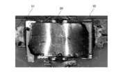
- a device according to the configuration shown in FIG. 10 was prepared. Specifically, as shown in FIGS. 11 to 13, two wedge members 51 and 52 corresponding to the above-described wedge members 41 and 42 are prepared as the stand-off material 40, and the wedge members 51 and 52 are elastic.
- the elastic member 20 ′ was inserted into the lower surface of the member 20 ′, and the central portion of the elastic member 20 ′ was bent and urged in a substantially U-shape.
- the elastic member 20 ′ is made of a flat plate made of hyperphosphor bronze C5191-H and has a thickness of 0.05 mm, a width of about 2.5 mm, and a length of about 5 mm.
- Such a protective element was actually heated using a predetermined heat generation operation test apparatus, and the current interruption operation was evaluated.
- the test apparatus is provided with a heater corresponding to the heating resistor 12, and when the current flows through the energization path of the protective element, the heater generates heat.
- the resistance value of the heater is 13.03 ⁇ .
- energization was performed with an operating power of 22 W.
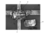
- FIG. 14 it was confirmed that the elastic member 20 ′ jumped greatly after 0.43 milliseconds from the start of energization.
- the heater resistance value after the operation was 13.0 ⁇ , and the resistance value of the protective element was infinite, confirming that the current interruption operation was performed reliably.
Landscapes
- Fuses (AREA)
Priority Applications (3)
| Application Number | Priority Date | Filing Date | Title |
|---|---|---|---|
| US12/988,199 US8767368B2 (en) | 2008-04-21 | 2009-03-02 | Protective element and method for producing the same |
| CN2009801140586A CN102027560B (zh) | 2008-04-21 | 2009-03-02 | 保护元件及其制造方法 |
| KR1020107025315A KR101291928B1 (ko) | 2008-04-21 | 2009-03-02 | 보호 소자 및 그 제조 방법 |
Applications Claiming Priority (2)
| Application Number | Priority Date | Filing Date | Title |
|---|---|---|---|
| JP2008109779A JP5117917B2 (ja) | 2008-04-21 | 2008-04-21 | 保護素子及びその製造方法 |
| JP2008-109779 | 2008-04-21 |
Publications (1)
| Publication Number | Publication Date |
|---|---|
| WO2009130946A1 true WO2009130946A1 (ja) | 2009-10-29 |
Family
ID=41216687
Family Applications (1)
| Application Number | Title | Priority Date | Filing Date |
|---|---|---|---|
| PCT/JP2009/053870 Ceased WO2009130946A1 (ja) | 2008-04-21 | 2009-03-02 | 保護素子及びその製造方法 |
Country Status (6)
| Country | Link |
|---|---|
| US (1) | US8767368B2 (https=) |
| JP (1) | JP5117917B2 (https=) |
| KR (1) | KR101291928B1 (https=) |
| CN (1) | CN102027560B (https=) |
| TW (1) | TW201003704A (https=) |
| WO (1) | WO2009130946A1 (https=) |
Cited By (6)
| Publication number | Priority date | Publication date | Assignee | Title |
|---|---|---|---|---|
| JP2011181667A (ja) * | 2010-03-01 | 2011-09-15 | Sumitomo Bakelite Co Ltd | 半導体装置の製造方法、半導体装置、および電子部品の製造方法および電子部品 |
| CN102668729A (zh) * | 2009-11-06 | 2012-09-12 | 罗伯特·博世有限公司 | 电子元器件 |
| WO2013025398A1 (en) * | 2011-08-12 | 2013-02-21 | Tyco Electronics Corporation | Reflowable circuit protection device |
| US8941461B2 (en) | 2011-02-02 | 2015-01-27 | Tyco Electronics Corporation | Three-function reflowable circuit protection device |
| US9455106B2 (en) | 2011-02-02 | 2016-09-27 | Littelfuse, Inc. | Three-function reflowable circuit protection device |
| WO2024018863A1 (ja) * | 2022-07-20 | 2024-01-25 | デクセリアルズ株式会社 | 保護素子 |
Families Citing this family (37)
| Publication number | Priority date | Publication date | Assignee | Title |
|---|---|---|---|---|
| JP5351860B2 (ja) | 2009-09-04 | 2013-11-27 | 乾坤科技股▲ふん▼有限公司 | 保護装置 |
| US9025295B2 (en) | 2009-09-04 | 2015-05-05 | Cyntec Co., Ltd. | Protective device and protective module |
| JP5192524B2 (ja) | 2009-09-04 | 2013-05-08 | 乾坤科技股▲ふん▼有限公司 | 保護装置 |
| US8531263B2 (en) | 2009-11-24 | 2013-09-10 | Littelfuse, Inc. | Circuit protection device |
| JP5260592B2 (ja) | 2010-04-08 | 2013-08-14 | デクセリアルズ株式会社 | 保護素子、バッテリ制御装置、及びバッテリパック |
| US20120194958A1 (en) * | 2011-02-02 | 2012-08-02 | Matthiesen Martyn A | Three-Function Reflowable Circuit Protection Device |
| JP5667468B2 (ja) * | 2011-02-21 | 2015-02-12 | 日本特殊陶業株式会社 | グロープラグの通電制御装置 |
| JP5896412B2 (ja) * | 2012-05-17 | 2016-03-30 | エヌイーシー ショット コンポーネンツ株式会社 | 保護素子用ヒューズ素子およびそれを利用した回路保護素子 |
| DE102012010483A1 (de) * | 2012-05-26 | 2013-11-28 | Brose Fahrzeugteile GmbH & Co. Kommanditgesellschaft, Würzburg | Bürstensystem für einen Elektromotor |
| US9082737B2 (en) * | 2012-11-15 | 2015-07-14 | Infineon Technologies Ag | System and method for an electronic package with a fail-open mechanism |
| DE102013013662A1 (de) * | 2013-08-16 | 2015-02-19 | Audi Ag | Sicherungsvorrichtung |
| JP6254859B2 (ja) * | 2014-01-24 | 2017-12-27 | デクセリアルズ株式会社 | 遮断素子、遮断素子回路、 |
| TWI588857B (zh) * | 2014-02-10 | 2017-06-21 | 陳莎莉 | 複合式保護元件與保護電路 |
| CN104835702B (zh) * | 2014-02-10 | 2017-05-24 | 陈莎莉 | 复合式保护元件 |
| JP6381975B2 (ja) * | 2014-06-04 | 2018-08-29 | デクセリアルズ株式会社 | 短絡素子 |
| JP6381980B2 (ja) * | 2014-06-11 | 2018-08-29 | デクセリアルズ株式会社 | スイッチ素子及びスイッチ回路 |
| JP6343201B2 (ja) * | 2014-08-04 | 2018-06-13 | デクセリアルズ株式会社 | 短絡素子 |
| TWI562493B (en) * | 2015-07-20 | 2016-12-11 | Amita Technologies Inc Ltd | Battery Protection System and Initiative Fuse Protective Devices thereof |
| JP6708387B2 (ja) * | 2015-10-07 | 2020-06-10 | デクセリアルズ株式会社 | スイッチ素子、電子部品、バッテリシステム |
| JP6739922B2 (ja) * | 2015-10-27 | 2020-08-12 | デクセリアルズ株式会社 | ヒューズ素子 |
| WO2017121474A1 (en) * | 2016-01-14 | 2017-07-20 | Schurter Ag | Mechanically activatable thermal fuse |
| US20170236667A1 (en) * | 2016-02-17 | 2017-08-17 | Dexerials Corporation | Protective element and protective circuit substrate using the same |
| TW201740605A (zh) * | 2017-01-23 | 2017-11-16 | Pao-Hsuan Chen | 保護元件與二次電池包 |
| TW201740417A (zh) * | 2017-07-07 | 2017-11-16 | Pao-Hsuan Chen | 開關元件 |
| CN110120557B (zh) * | 2018-02-05 | 2021-01-15 | 宁德新能源科技有限公司 | 保护装置及电池 |
| TWI677889B (zh) * | 2018-07-03 | 2019-11-21 | 易湘雲 | 鉍基合金作為開關或插座斷電元件的方法 |
| TWI676198B (zh) * | 2018-07-03 | 2019-11-01 | 易湘雲 | 翹板開關及其滑動壓抵件 |
| JP7173902B2 (ja) * | 2019-03-05 | 2022-11-16 | デクセリアルズ株式会社 | 保護素子 |
| FR3095305B1 (fr) * | 2019-04-16 | 2022-03-11 | G Cartier Tech | Dispositif de commande securise pour actionneur electrique |
| JP7340979B2 (ja) * | 2019-07-22 | 2023-09-08 | デクセリアルズ株式会社 | 保護素子および保護回路 |
| JP7369049B2 (ja) * | 2020-01-31 | 2023-10-25 | 日立Astemo株式会社 | モータ駆動装置 |
| JP7602335B2 (ja) * | 2020-08-28 | 2024-12-18 | 日立Astemo株式会社 | モータ駆動装置 |
| JP7468431B2 (ja) | 2021-03-30 | 2024-04-16 | 株式会社オートネットワーク技術研究所 | ヒューズ素子 |
| CN113394518A (zh) * | 2021-05-07 | 2021-09-14 | 恒大新能源技术(深圳)有限公司 | 电池模组 |
| CN117098348A (zh) * | 2022-05-11 | 2023-11-21 | 台达电子工业股份有限公司 | 高低压转换电路的承载结构 |
| CN116130315B (zh) * | 2022-12-27 | 2025-10-28 | 上海维安电子股份有限公司 | 一种保护元件 |
| CN115910697B (zh) * | 2022-12-29 | 2024-08-02 | 惠州市良胜电子有限公司 | 三端保险丝制备方法及三端保险丝 |
Citations (6)
| Publication number | Priority date | Publication date | Assignee | Title |
|---|---|---|---|---|
| JPS5714340U (https=) * | 1980-06-26 | 1982-01-25 | ||
| JPS57107530A (en) * | 1980-12-25 | 1982-07-05 | Nippon Electric Co | Overcurrent protecting element |
| JPS6040999U (ja) * | 1983-08-29 | 1985-03-22 | 松下電器産業株式会社 | 温度過昇防止装置 |
| JPS6455294U (https=) * | 1987-10-01 | 1989-04-05 | ||
| JPH031418A (ja) * | 1989-05-30 | 1991-01-08 | Tachibana Kinzoku Kogyo Kk | 温度ヒューズ |
| JP2004363630A (ja) * | 2004-08-30 | 2004-12-24 | Sony Chem Corp | 保護素子の実装方法 |
Family Cites Families (16)
| Publication number | Priority date | Publication date | Assignee | Title |
|---|---|---|---|---|
| US3763454A (en) * | 1972-02-22 | 1973-10-02 | Tektronix Inc | Thermal switch |
| US3796981A (en) * | 1972-09-05 | 1974-03-12 | Kidde & Co Walter | Fail safe thermostatic switch |
| DK385277A (da) | 1976-09-21 | 1978-03-22 | B Spreafico | Fremgangsmaade og maskine til mekanisk dekapering af traad ved valsning |
| JPS5852792B2 (ja) | 1978-12-27 | 1983-11-25 | 瓜生製作株式会社 | 油圧トルクレンチのトルク規制装置 |
| JPS609815B2 (ja) * | 1980-07-01 | 1985-03-13 | テルモ株式会社 | 医療器具の防カビ方法 |
| JPS58133873A (ja) | 1982-02-05 | 1983-08-09 | Asahi Glass Co Ltd | 防食被覆方法 |
| JPS62149335A (ja) | 1985-12-24 | 1987-07-03 | Nippon Shokubai Kagaku Kogyo Co Ltd | 吸水剤 |
| DE19530413C1 (de) * | 1995-08-18 | 1997-04-03 | Heraeus Sensor Gmbh | Verfahren zur Befestigung und Kontaktierung von Widerstandselementen für Heißfilmanemometer sowie Sensoranordnung |
| JPH0992110A (ja) * | 1995-09-26 | 1997-04-04 | Denso Corp | 温度ヒューズ付抵抗器 |
| JP3993256B2 (ja) | 1996-05-08 | 2007-10-17 | ニチコン株式会社 | 過電圧・過電流保護装置 |
| JP2000306477A (ja) * | 1999-04-16 | 2000-11-02 | Sony Chem Corp | 保護素子 |
| JP2005129352A (ja) * | 2003-10-23 | 2005-05-19 | Nec Schott Components Corp | 抵抗付き温度ヒュ−ズ |
| JP2005288458A (ja) * | 2004-03-31 | 2005-10-20 | Toshiba Corp | 接合体、半導体装置、接合方法、及び半導体装置の製造方法 |
| CN101155830B (zh) | 2005-02-04 | 2014-06-18 | 雷文生物技术公司 | 结合epha2的抗体及其使用方法 |
| US7426117B2 (en) * | 2005-12-21 | 2008-09-16 | Xerox Corporation | Chip on a board |
| US20100013591A1 (en) * | 2006-05-17 | 2010-01-21 | Hiroyuki Koyama | Protection Device |
-
2008
- 2008-04-21 JP JP2008109779A patent/JP5117917B2/ja active Active
-
2009
- 2009-03-02 US US12/988,199 patent/US8767368B2/en active Active
- 2009-03-02 TW TW098106752A patent/TW201003704A/zh unknown
- 2009-03-02 CN CN2009801140586A patent/CN102027560B/zh active Active
- 2009-03-02 WO PCT/JP2009/053870 patent/WO2009130946A1/ja not_active Ceased
- 2009-03-02 KR KR1020107025315A patent/KR101291928B1/ko active Active
Patent Citations (6)
| Publication number | Priority date | Publication date | Assignee | Title |
|---|---|---|---|---|
| JPS5714340U (https=) * | 1980-06-26 | 1982-01-25 | ||
| JPS57107530A (en) * | 1980-12-25 | 1982-07-05 | Nippon Electric Co | Overcurrent protecting element |
| JPS6040999U (ja) * | 1983-08-29 | 1985-03-22 | 松下電器産業株式会社 | 温度過昇防止装置 |
| JPS6455294U (https=) * | 1987-10-01 | 1989-04-05 | ||
| JPH031418A (ja) * | 1989-05-30 | 1991-01-08 | Tachibana Kinzoku Kogyo Kk | 温度ヒューズ |
| JP2004363630A (ja) * | 2004-08-30 | 2004-12-24 | Sony Chem Corp | 保護素子の実装方法 |
Cited By (9)
| Publication number | Priority date | Publication date | Assignee | Title |
|---|---|---|---|---|
| CN102668729A (zh) * | 2009-11-06 | 2012-09-12 | 罗伯特·博世有限公司 | 电子元器件 |
| JP2013509733A (ja) * | 2009-11-06 | 2013-03-14 | ローベルト ボッシュ ゲゼルシャフト ミット ベシュレンクテル ハフツング | 電子部品 |
| US8749940B2 (en) | 2009-11-06 | 2014-06-10 | Robert Bosch Gmbh | Electronic component |
| JP2011181667A (ja) * | 2010-03-01 | 2011-09-15 | Sumitomo Bakelite Co Ltd | 半導体装置の製造方法、半導体装置、および電子部品の製造方法および電子部品 |
| US8941461B2 (en) | 2011-02-02 | 2015-01-27 | Tyco Electronics Corporation | Three-function reflowable circuit protection device |
| US9455106B2 (en) | 2011-02-02 | 2016-09-27 | Littelfuse, Inc. | Three-function reflowable circuit protection device |
| WO2013025398A1 (en) * | 2011-08-12 | 2013-02-21 | Tyco Electronics Corporation | Reflowable circuit protection device |
| US9620318B2 (en) | 2011-08-12 | 2017-04-11 | Littlefuse, Inc. | Reflowable circuit protection device |
| WO2024018863A1 (ja) * | 2022-07-20 | 2024-01-25 | デクセリアルズ株式会社 | 保護素子 |
Also Published As
| Publication number | Publication date |
|---|---|
| US8767368B2 (en) | 2014-07-01 |
| TW201003704A (en) | 2010-01-16 |
| KR20110015547A (ko) | 2011-02-16 |
| CN102027560A (zh) | 2011-04-20 |
| US20110211284A1 (en) | 2011-09-01 |
| JP2009259724A (ja) | 2009-11-05 |
| KR101291928B1 (ko) | 2013-07-31 |
| JP5117917B2 (ja) | 2013-01-16 |
| TWI373060B (https=) | 2012-09-21 |
| CN102027560B (zh) | 2013-12-04 |
Similar Documents
| Publication | Publication Date | Title |
|---|---|---|
| JP5117917B2 (ja) | 保護素子及びその製造方法 | |
| KR101167543B1 (ko) | 보호 소자 | |
| JP5301298B2 (ja) | 保護素子 | |
| CN100461321C (zh) | 保护元件 | |
| CN102217021B (zh) | 保护元件 | |
| US8976001B2 (en) | Protective device | |
| US20100176910A1 (en) | Fusible alloy element, thermal fuse with fusible alloy element and method for producing a thermal fuse | |
| US11145480B2 (en) | Fuse device | |
| CN107004538A (zh) | 安装体的制造方法、温度熔丝器件的安装方法以及温度熔丝器件 | |
| US11640892B2 (en) | Fuse element and protective element | |
| CN111725793B (zh) | 过电压保护装置 | |
| JP2010165685A (ja) | 保護素子及びバッテリーパック | |
| KR20160009517A (ko) | 온도 퓨즈 및 이를 구비한 인쇄회로기판 | |
| KR20190141719A (ko) | 보호 소자 | |
| JP7540044B2 (ja) | 保護素子 | |
| JP2013258013A (ja) | ヒューズ | |
| JP2014044955A (ja) | 保護素子及びバッテリーパック | |
| JP2012059719A (ja) | 保護素子及びバッテリーパック | |
| JP6711704B2 (ja) | バイパス電極付き保護素子 | |
| CN113711454B (zh) | 用于过电压保护的装置 | |
| WO2013000796A2 (en) | Electric device | |
| JP2015032423A (ja) | ヒューズ | |
| HK1088116B (en) | Protection element | |
| JPH051144U (ja) | 温度ヒユーズ |
Legal Events
| Date | Code | Title | Description |
|---|---|---|---|
| WWE | Wipo information: entry into national phase |
Ref document number: 200980114058.6 Country of ref document: CN |
|
| 121 | Ep: the epo has been informed by wipo that ep was designated in this application |
Ref document number: 09734404 Country of ref document: EP Kind code of ref document: A1 |
|
| NENP | Non-entry into the national phase |
Ref country code: DE |
|
| ENP | Entry into the national phase |
Ref document number: 20107025315 Country of ref document: KR Kind code of ref document: A |
|
| WWE | Wipo information: entry into national phase |
Ref document number: 12988199 Country of ref document: US |
|
| 122 | Ep: pct application non-entry in european phase |
Ref document number: 09734404 Country of ref document: EP Kind code of ref document: A1 |