WO2009104752A1 - 表示媒体用粒子、それを用いた情報表示用パネルおよび表示媒体用粒子の製造方法 - Google Patents
表示媒体用粒子、それを用いた情報表示用パネルおよび表示媒体用粒子の製造方法 Download PDFInfo
- Publication number
- WO2009104752A1 WO2009104752A1 PCT/JP2009/053069 JP2009053069W WO2009104752A1 WO 2009104752 A1 WO2009104752 A1 WO 2009104752A1 JP 2009053069 W JP2009053069 W JP 2009053069W WO 2009104752 A1 WO2009104752 A1 WO 2009104752A1
- Authority
- WO
- WIPO (PCT)
- Prior art keywords
- particles
- display medium
- display
- particle
- information
- Prior art date
- Legal status (The legal status is an assumption and is not a legal conclusion. Google has not performed a legal analysis and makes no representation as to the accuracy of the status listed.)
- Ceased
Links
Images



Classifications
-
- G—PHYSICS
- G02—OPTICS
- G02F—OPTICAL DEVICES OR ARRANGEMENTS FOR THE CONTROL OF LIGHT BY MODIFICATION OF THE OPTICAL PROPERTIES OF THE MEDIA OF THE ELEMENTS INVOLVED THEREIN; NON-LINEAR OPTICS; FREQUENCY-CHANGING OF LIGHT; OPTICAL LOGIC ELEMENTS; OPTICAL ANALOGUE/DIGITAL CONVERTERS
- G02F1/00—Devices or arrangements for the control of the intensity, colour, phase, polarisation or direction of light arriving from an independent light source, e.g. switching, gating or modulating; Non-linear optics
- G02F1/01—Devices or arrangements for the control of the intensity, colour, phase, polarisation or direction of light arriving from an independent light source, e.g. switching, gating or modulating; Non-linear optics for the control of the intensity, phase, polarisation or colour
- G02F1/165—Devices or arrangements for the control of the intensity, colour, phase, polarisation or direction of light arriving from an independent light source, e.g. switching, gating or modulating; Non-linear optics for the control of the intensity, phase, polarisation or colour based on translational movement of particles in a fluid under the influence of an applied field
- G02F1/166—Devices or arrangements for the control of the intensity, colour, phase, polarisation or direction of light arriving from an independent light source, e.g. switching, gating or modulating; Non-linear optics for the control of the intensity, phase, polarisation or colour based on translational movement of particles in a fluid under the influence of an applied field characterised by the electro-optical or magneto-optical effect
- G02F1/167—Devices or arrangements for the control of the intensity, colour, phase, polarisation or direction of light arriving from an independent light source, e.g. switching, gating or modulating; Non-linear optics for the control of the intensity, phase, polarisation or colour based on translational movement of particles in a fluid under the influence of an applied field characterised by the electro-optical or magneto-optical effect by electrophoresis
-
- B—PERFORMING OPERATIONS; TRANSPORTING
- B82—NANOTECHNOLOGY
- B82Y—SPECIFIC USES OR APPLICATIONS OF NANOSTRUCTURES; MEASUREMENT OR ANALYSIS OF NANOSTRUCTURES; MANUFACTURE OR TREATMENT OF NANOSTRUCTURES
- B82Y20/00—Nanooptics, e.g. quantum optics or photonic crystals
-
- B—PERFORMING OPERATIONS; TRANSPORTING
- B82—NANOTECHNOLOGY
- B82Y—SPECIFIC USES OR APPLICATIONS OF NANOSTRUCTURES; MEASUREMENT OR ANALYSIS OF NANOSTRUCTURES; MANUFACTURE OR TREATMENT OF NANOSTRUCTURES
- B82Y30/00—Nanotechnology for materials or surface science, e.g. nanocomposites
-
- G—PHYSICS
- G02—OPTICS
- G02F—OPTICAL DEVICES OR ARRANGEMENTS FOR THE CONTROL OF LIGHT BY MODIFICATION OF THE OPTICAL PROPERTIES OF THE MEDIA OF THE ELEMENTS INVOLVED THEREIN; NON-LINEAR OPTICS; FREQUENCY-CHANGING OF LIGHT; OPTICAL LOGIC ELEMENTS; OPTICAL ANALOGUE/DIGITAL CONVERTERS
- G02F1/00—Devices or arrangements for the control of the intensity, colour, phase, polarisation or direction of light arriving from an independent light source, e.g. switching, gating or modulating; Non-linear optics
- G02F1/01—Devices or arrangements for the control of the intensity, colour, phase, polarisation or direction of light arriving from an independent light source, e.g. switching, gating or modulating; Non-linear optics for the control of the intensity, phase, polarisation or colour
- G02F1/13—Devices or arrangements for the control of the intensity, colour, phase, polarisation or direction of light arriving from an independent light source, e.g. switching, gating or modulating; Non-linear optics for the control of the intensity, phase, polarisation or colour based on liquid crystals, e.g. single liquid crystal display cells
- G02F1/133—Constructional arrangements; Operation of liquid crystal cells; Circuit arrangements
- G02F1/1333—Constructional arrangements; Manufacturing methods
- G02F1/1339—Gaskets; Spacers; Sealing of cells
- G02F1/13394—Gaskets; Spacers; Sealing of cells spacers regularly patterned on the cell subtrate, e.g. walls, pillars
-
- G—PHYSICS
- G02—OPTICS
- G02F—OPTICAL DEVICES OR ARRANGEMENTS FOR THE CONTROL OF LIGHT BY MODIFICATION OF THE OPTICAL PROPERTIES OF THE MEDIA OF THE ELEMENTS INVOLVED THEREIN; NON-LINEAR OPTICS; FREQUENCY-CHANGING OF LIGHT; OPTICAL LOGIC ELEMENTS; OPTICAL ANALOGUE/DIGITAL CONVERTERS
- G02F1/00—Devices or arrangements for the control of the intensity, colour, phase, polarisation or direction of light arriving from an independent light source, e.g. switching, gating or modulating; Non-linear optics
- G02F1/01—Devices or arrangements for the control of the intensity, colour, phase, polarisation or direction of light arriving from an independent light source, e.g. switching, gating or modulating; Non-linear optics for the control of the intensity, phase, polarisation or colour
- G02F1/165—Devices or arrangements for the control of the intensity, colour, phase, polarisation or direction of light arriving from an independent light source, e.g. switching, gating or modulating; Non-linear optics for the control of the intensity, phase, polarisation or colour based on translational movement of particles in a fluid under the influence of an applied field
- G02F1/1675—Constructional details
- G02F2001/1678—Constructional details characterised by the composition or particle type
Definitions
- the present invention provides a display medium enclosed between two opposing substrates, at least one of which is transparent, as particles constituting a display medium used for an information display panel that displays information such as images by moving the display medium
- the present invention relates to a display medium particle, an information display panel using the same, and a method for producing a display medium particle.
- an information display panel used for a charged particle driving type information display device a display medium configured as a group of particles containing chargeable particles is enclosed in a space between two opposing substrates, at least one of which is transparent,
- an information display panel that displays information such as an image by moving the display medium by applying an electric field to the display medium (see, for example, pamphlet of International Publication No. 2003/050606).
- the particles obtained by kneading, pulverizing, and classifying using electrophotographic toner or conventional configurations and materials are used as display medium particles constituting the display medium, display is performed.
- the particles are pressed against the substrate by the mirror image attraction due to the charged charges of the medium particles and deformed by bending, and the adhesion area between the display medium particles and the panel substrate increases, resulting in high adhesion to the substrate, resulting in high contrast display. It has been difficult to achieve the above and to reduce the driving voltage.
- the surface of the display medium particles on the surface of the particles due to the mechanical stress acting by the collision between the display medium particles or the collision between the display medium particles and the electrode plate.
- the adhered fine particles are embedded in the particles. For this reason, the adhesion between the display medium particles and the substrate is increased, the flow characteristics of the display medium particles are deteriorated, and the charging characteristics are changed, so that the initial display performance may not be maintained.
- the object of the present invention is to solve the above-mentioned problems and suppress the child particles from being peeled off from the mother particles when the child particles are uniformly embedded on the surface of the mother particles and the display is repeatedly rewritten during manufacturing.
- Another object of the present invention is to provide a composite type display medium particle and an information display panel using the same.
- the present inventors have attached or fixed the child particles to the surface of the mother particles obtained by spheroidizing the pulverized particles by heat treatment.
- the present invention has been completed by finding that it can be uniformly embedded in the particle surface and that the child particles can be prevented from peeling off.
- the display medium particles of the present invention are used for an information display panel in which a display medium is sealed between two opposing substrates, at least one of which is transparent, and the display medium is moved to display information such as an image.
- Particles for a display medium constituting the medium wherein the particles produced by kneading, pulverizing, and classifying the raw material containing the resin are adhered or fixed to the surface of the mother particles obtained by spheronizing the particles by heat treatment. It consists of the obtained composite type particles.
- the information display panel of the present invention is characterized in that the display medium particles are used as a display medium.
- an information display panel for enclosing a display medium between two opposing substrates, at least one of which is transparent, and displaying information such as an image by moving the display medium A method for producing particles for a display medium constituting a display medium used in the above, wherein particles are produced by kneading, pulverizing, and classifying a raw material containing a resin, and the produced particles are spheroidized by heat treatment to obtain mother particles, Display medium particles made of composite particles are obtained by attaching or fixing child particles to the surface of the obtained mother particles.
- the present invention it is possible to obtain particles for a display medium in which the child particles are uniformly embedded on the surface of the mother particle, the child particles are not easily peeled off, and the charging characteristics are stabilized and the durability in display rewriting is improved.
- the display medium particles as a display medium, there is an advantageous effect that durability can be improved while maintaining initial display performance even when display rewriting is performed.
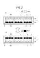
- (A), (b) is a figure which shows an example of the information display panel used as the object of this invention, respectively.
- (A), (b) is a figure which shows the other example of the information display panel used as the object of this invention, respectively.
- (A), (b) is a figure which shows the further another example of the information display panel used as the object of this invention, respectively.
- (A)-(d) is a figure which shows the further another example of the information display panel used as the object of this invention, respectively.
- (A), (b) is a figure which shows the further another example of the information display panel used as the object of this invention, respectively.
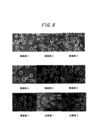
- It is a figure which shows an example of the shape of the partition in the information display panel used as the object of this invention. 4 is an SEM photograph of mother particles of display medium particles of Examples 1 to 7 and Comparative Example of the present invention.
- the present invention will be described in detail.
- an electric field is applied to a display medium configured as a particle group including particles for display medium sealed between two opposing substrates.
- the display medium is attracted by the force of the electric field, the Coulomb force, or the like, and the display medium changes the moving direction according to the change in the electric field direction, whereby information such as an image is displayed. Therefore, it is necessary to design the information display panel so that the display medium can move uniformly and maintain stability when rewriting the display repeatedly or when displaying the display information continuously.
- the force applied to the particles constituting the display medium in addition to the force attracting each other by the Coulomb force between the particles, an electric mirror image force between the electrode and the substrate, an intermolecular force, a liquid cross-linking force, gravity and the like can be considered.
- the optical reflectance and charging characteristics of each other are configured as a particle group composed of at least one kind of particles including particles having optical reflectance and chargeability.
- At least two or more different display media are enclosed between substrates (here, a white display medium 3W consisting of particles of white display medium particles 3Wa and a black display medium 3B consisting of particles of black display medium particles 3Ba are shown).
- each cell formed by the partition walls 4 depending on the electric field generated by applying a voltage between the electrode 5 (individual electrode) provided on the substrate 1 and the electrode 6 (individual electrode) provided on the substrate 2.
- the substrate 1 and 2 are moved vertically.
- the white display medium 3W is visually recognized by the observer and white dot display is performed, or as shown in FIG. 1B, the black display medium 3B is visually recognized by the observer. Black dots are displayed.
- the partition in front is abbreviate
- the optical reflectivity and the charging characteristics of each other are configured as a particle group composed of at least one kind of particles including particles having optical reflectivity and chargeability.
- At least two or more types of display media different from each other here, a white display medium 3W composed of particles of white display medium particles 3Wa and a black display medium 3B composed of particles of black display medium particles 3Ba are shown) between substrates.
- a voltage is applied between an electrode 5 (line electrode) provided on the substrate 1 and an electrode 6 (line electrode) provided on the substrate 2 in accordance with an electric field generated.
- the substrate 1 and 2 are moved vertically. Then, as shown in FIG.
- the white display medium 3W is visually recognized by the observer and white dot display is performed, or as shown in FIG. 2B, the black display medium 3B is visually recognized by the observer. Black dots are displayed.
- the partition in front is abbreviate
- one type of display medium configured as a particle group including at least one type of particles including particles having optical reflectance and chargeability (here, white) (Showing white display medium 3W composed of particles of display medium particles 3Wa) between each substrate formed between the substrates and formed by the partition walls 4, the electrode 5 provided on the substrate 1 and the electrode 6 provided on the substrate 2 The substrate is moved in a direction parallel to the substrates 1 and 2 in accordance with an electric field generated by applying a voltage therebetween. Then, as shown in FIG. 3 (a), the white display medium 3W is visually recognized by the observer and white dot display is performed, or the color of the black plate 7 is shown to the observer as shown in FIG. 3 (b). A black dot is displayed by visual recognition.
- the partition in front is abbreviate
- At least one kind of particles including particles having optical reflectivity and chargeability are used.
- At least two kinds of display media having different optical reflectivity and charging characteristics from each other here, white display medium 3W composed of particles of white display medium particles 3Wa and black display medium particles 3Ba).
- the external electric field forming means 11 provided outside the substrate 1 and the external electric field provided outside the substrate 2
- the substrate is moved perpendicularly to the substrates 1 and 2 in accordance with an electric field generated by applying a voltage between the forming unit 12 and the forming unit 12.
- the white display medium 3W is visually recognized by the observer and white dot display is performed, or as shown in FIG. 2D, the black display medium 3B is visually recognized by the observer. Black dots are displayed.
- the front partition is omitted.
- a conductive member 13 is provided inside the substrate 1, and a conductive member 14 is provided inside the substrate 2. This conductive member may not be provided.
- FIGS. 5A and 5B an example of color display in which a display unit (1 dot) is configured by three cells is shown.
- the display medium all the cells 21-1 to 21-3 are filled with the white display medium 3W and the black display medium 3B, and the first cell 21-1 is filled.
- a red color filter 22R is provided on the viewer side
- a green color filter 22G is provided on the viewer side of the second cell 21-2
- a blue color filter 22BL is provided on the viewer side of the third cell 21-3.
- a display unit is composed of three cells, the first cell 21-1, the second cell 21-2, and the third cell 21-3. In this example, as shown in FIG.
- the white display medium 3W is moved in the first cell 21-1 to the third cell 21-3 to the viewer side to the viewer.
- the black display medium 3B By performing white dot display or moving the black display medium 3B in all the first cells 21-1 to 21-3 to the viewer side as shown in FIG. 5B. Black dots are displayed to the observer.
- the partition in front is abbreviate
- FIGS. 6A and 6B are diagrams showing examples of the display medium particles of the present invention.
- the display medium particle 31 of the present invention is characterized in that the child particles 33 are attached to the surface of the mother particle 32 obtained by spheroidizing the pulverized particles by heat treatment.
- FIG. 6A shows an example in which a composite particle is formed by fixing a child particle 33 to the surface of the mother particle 32
- FIG. 6B shows a composite where the child particle 33 is attached to the surface of the mother particle 32.
- attachment means that the child particle 33 is fixed to the surface of the mother particle 32 by electrostatic force, Coulomb force, van der Waals force, etc., and therefore the child particle 33 moves when the display is rewritten repeatedly.
- adherence means that the child particles 33 are embedded in the surface of the mother particles 32, fixed by adhesion, adhesion, etc., and therefore the child particles 33 are moved when the display is rewritten repeatedly. Means nothing.
- the display medium particles 31 are used as display medium particles constituting at least one display medium of the information display panels shown in FIGS. 1 (a), 1 (b) to 5 (a), 5 (b). Therefore, at least one of the information display panels constitutes a display medium having color and chargeability in a space between two transparent substrates and is sealed.
- the display medium particle 31 of the present invention as the mother particle 32, by applying particles obtained by spheroidizing particles prepared by kneading, pulverizing, and classifying a raw material containing a resin, 33 can be uniformly adhered or fixed, and the child particles 33 can be prevented from peeling off when the display medium particles 31 are manufactured or when the display is rewritten repeatedly.
- kneading, pulverization, and classification of the raw material containing the resin can be performed by a conventional method.
- the particles obtained by kneading, pulverizing, and classifying the raw material containing the resin are spheroidized by heat treatment.
- the spheroidization of the particles by heat treatment is performed by jetting and dispersing the particles in hot air. It is preferable to carry out by making the particles into a molten state by spheroidization by surface tension.
- the spheronization by such heat treatment can be performed by, for example, a commercially available particle spheronization apparatus.
- the heat treatment temperature is preferably in the range of 400 to 700 ° C. If it is less than 400 ° C., it does not melt sufficiently and may not be spheroidized, and if it exceeds 700 ° C., the resin may be greatly deteriorated.
- the progress of the spheroidization of the particles by the heat treatment can be compared by observing the shape of the particles after spheronization and calculating the sphericity.
- the projected image of each particle is photographed, and the area and perimeter are measured by image processing.
- Sphericality perimeter of a circle with the same area as the particle projection image / perimeter of the particle projection image That is, if the particle is a perfect circle, the sphericity is 1, and the spheroidization progresses as the sphericity value approaches 1. It can be judged.
- the sphericity is preferably 0.950 or more, more preferably 0.970 or more. If the sphericity is less than 0.950, the child particles may not be embedded uniformly and the object of the present invention may not be achieved.
- the substrate As for the substrate, at least one of the substrates is a transparent substrate 2 on which the color of the display medium can be confirmed from the outside of the information display panel, and a material having high visible light transmittance and good heat resistance is suitable.
- the substrate 1 may be transparent or opaque.
- substrate materials include polymer sheets such as polyethylene terephthalate, polyethylene naphthalate, polyethersulfone, polyethylene, polycarbonate, polyimide, and acrylic, flexible materials such as metal sheets, and glass and quartz.
- An inorganic sheet having no flexibility is mentioned.
- the thickness of the substrate is preferably 2 to 5000 ⁇ m, and more preferably 5 to 2000 ⁇ m. If it is too thin, it will be difficult to maintain the strength and uniformity of the distance between the substrates. Is inconvenient.
- metals such as aluminum, silver, nickel, copper, and gold, indium tin oxide (ITO), indium oxide, antimony tin oxide (ATO) ), Conductive metal oxides such as zinc-doped indium oxide (IZO), aluminum-doped zinc oxide (AZO), conductive tin oxide, and conductive zinc oxide, and conductive polymers such as polyaniline, polypyrrole, and polythiophene. It is appropriately selected and used.
- a method for forming an electrode a method of forming the above-described materials into a thin film by sputtering, vacuum deposition, CVD (chemical vapor deposition), coating, or the like, or a method of laminating a metal foil (for example, rolled copper foil)
- a method in which the conductive member is mixed with a solvent or a synthetic resin binder and applied a method in which the conductive member is mixed with a solvent or a synthetic resin binder and applied.
- the electrode provided on the display surface side substrate 2 which is on the viewing side and needs to be transparent needs to be transparent, but the electrode provided on the back side substrate 1 does not need to be transparent.
- the above-mentioned material that can be patterned and is electrically conductive can be suitably used.
- the electrode thickness may be 0.01 to 10 ⁇ m, preferably 0.05 to 5 ⁇ m, as long as conductivity is ensured and light transmittance is not affected.
- the material and thickness of the electrode provided on the back side substrate 1 are the same as those of the electrode provided on the display surface side substrate described above, but need not be transparent. In this case, the external voltage input may be superimposed with direct current or alternating current.
- the shape of the partition wall 4 provided on the substrate as necessary is appropriately set according to the type of display medium involved in display, the shape and arrangement of the electrodes to be arranged, and is not limited in general.
- the partition wall height is adjusted to 100 ⁇ m, preferably 3 to 50 ⁇ m, and the height of the partition wall is adjusted to 10 to 500 ⁇ m, preferably 10 to 200 ⁇ m. Further, in order to obtain a high electric field by applying a low voltage, it is preferable that the distance between the substrates is small. Therefore, the height of the partition wall is adjusted to 10 to 100 ⁇ m, preferably 10 to 50 ⁇ m.
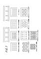
- the partition wall In forming the partition wall, a both-rib method in which ribs are formed on each of the opposing substrates 1 and 2 and then bonded, and a single-rib method in which ribs are formed only on one substrate are conceivable. In the present invention, any method is preferably used. As shown in FIG. 7, the cells formed by the partition walls made of these ribs are exemplified by a square shape, a triangular shape, a line shape, a circular shape, and a hexagonal shape as viewed from the substrate plane direction. And a mesh shape. It is better to make the portion corresponding to the cross section of the partition wall visible from the display surface side (the area of the cell frame) as small as possible, and the display becomes clearer.
- Examples of the method for forming the partition include a mold transfer method, a screen printing method, a sand blast method, a photolithography method, and an additive method. Any of these methods can be suitably used for the information display panel of the present invention, and among these, a photolithography method using a resist film and a mold transfer method are suitably used.
- the display medium particles 31 are used as the display medium by being composed of the display medium particles 31 as they are, or by being combined with other particles as the display medium.
- the base particles 32 constituting the display medium particles 31 may contain a charge control agent, a colorant, an inorganic additive, and the like, as necessary, in the resin as the main component, as necessary. . Examples of resins, charge control agents, colorants, and other additives will be given below.
- the resin examples include urethane resin, urea resin, acrylic resin, polyester resin, acrylic urethane resin, acrylic urethane silicone resin, acrylic urethane fluororesin, acrylic fluororesin, silicone resin, acrylic silicone resin, epoxy resin, polystyrene resin, styrene Acrylic resin, polyolefin resin, butyral resin, vinylidene chloride resin, melamine resin, phenol resin, fluororesin, polycarbonate resin, polysulfone resin, polyether resin, polyamide resin and the like can be mentioned, and two or more kinds can be mixed.
- styrene acrylic resin, acrylic resin, acrylic fluororesin, and polystyrene resin are preferable from the viewpoint of pulverization and spheronization.
- Examples of the positively chargeable charge control agent include charge control resins such as polyamine resins, tertiary amino group-containing copolymers, and quaternary ammonium base-containing copolymers, imidazole compounds, nigrosine dyes, quaternary ammonium salts, and triglycerides.
- An aminotriphenylmethane compound or the like can be used.
- negatively chargeable charge control agents examples include sulfonic acid group-containing copolymers, sulfonate group-containing copolymers, carboxylic acid group-containing copolymers, and charge control resins such as carboxylic acid group-containing copolymers, and Cr.
- Azo dyes containing metals represented by element symbols such as Co, Al, and Fe, salicylic acid metal compounds, and alkyl salicylic acid metal oxides.
- a charge control resin is preferably used, and the charge control resin preferably has a content of a functional group imparting chargeability of 0.5 to 15% by mass, and preferably 1 to 10%. More preferably, it is mass%.
- colorant various organic or inorganic pigments and dyes as exemplified below can be used.
- Black colorants include carbon black, copper oxide, manganese dioxide, aniline black, activated carbon and the like.
- C.I. I. Pigment blue 15 3
- C.I. I. Pigment Blue 15 Bituminous Blue, Cobalt Blue, Alkaline Blue Lake, Victoria Blue Lake, Phthalocyanine Blue, Metal-free Phthalocyanine Blue, Phthalocyanine Blue Partial Chlorides, Fast Sky Blue, Indanthrene Blue BC, and the like.
- red colorants include bengara, cadmium red, red lead, mercury sulfide, cadmium, permanent red 4R, risor red, pyrazolone red, watching red, calcium salt, lake red D, brilliant carmine 6B, eosin lake, rhodamine lake B, Alizarin Lake, Brilliant Carmine 3B, C.I. I. Pigment Red 2 etc.
- Yellow colorants include chrome yellow, zinc yellow, cadmium yellow, yellow iron oxide, mineral first yellow, nickel titanium yellow, navel yellow, naphthol yellow S, Hansa Yellow G, Hansa Yellow 10G, Benzidine Yellow G, Benzidine Yellow GR, Quinoline Yellow Lake, Permanent Yellow NCG, Tartrazine Lake, C.I. I. Pigment Yellow 12 etc.
- ⁇ Green colorants include chrome green, chromium oxide, pigment green B, C.I. I. Pigment Green 7, Malachite Green Lake, Final Yellow Green G, etc.
- Orange colorants include red yellow lead, molybdenum orange, permanent orange GTR, pyrazolone orange, Vulcan orange, indanthrene brilliant orange RK, benzidine orange G, indanthrene brilliant orange GK, C.I. I. Pigment Orange 31 etc.
- Purple colorants include manganese purple, first violet B, methyl violet lake and the like.
- white colorants include zinc white, titanium oxide, antimony white, and zinc sulfide.
- extender pigments examples include barite powder, barium carbonate, clay, silica, white carbon, talc, and alumina white.
- various dyes such as basic, acidic, disperse, and direct dyes include nigrosine, methylene blue, rose bengal, quinoline yellow, and ultramarine blue.
- inorganic additives include titanium oxide, zinc white, zinc sulfide, antimony oxide, calcium carbonate, lead white, talc, silica, calcium silicate, alumina white, cadmium yellow, cadmium red, cadmium orange, titanium yellow, Examples include bitumen, ultramarine blue, cobalt blue, cobalt green, cobalt violet, iron oxide, carbon black, manganese ferrite black, cobalt ferrite black, copper powder, and aluminum powder. These pigments and inorganic additives can be used alone or in combination. Of these, carbon black is particularly preferable as the black pigment, and titanium oxide is preferable as the white pigment.
- Examples of the material of the child particles 33 include resin materials such as polystyrene resin, acrylic resin, melamine resin, and phenol resin, and inorganic materials such as silica, alumina, and titanium oxide.
- the particles as the display medium of the present invention have an average particle diameter d (0.5) in the range of 1 to 20 ⁇ m and are uniform and uniform. If the average particle diameter d (0.5) is larger than this range, the display is not clear. If the average particle diameter d (0.5) is smaller than this range, the cohesive force between the particles becomes too large, which hinders movement as a display medium.
- the particle size distribution Span represented by the following formula is less than 5, preferably less than 3.
- Span (d (0.9) ⁇ d (0.1)) / d (0.5)
- d (0.5) is a numerical value expressing the particle diameter in ⁇ m that 50% of the particles are larger than this and 50% is smaller than this
- d (0.1) is a particle in which the ratio of the smaller particles is 10%.
- Numerical value expressed in ⁇ m and d (0.9) is a numerical value expressed in ⁇ m for a particle diameter of 90% or less.
- the above particle size distribution and particle size can be obtained from a laser diffraction / scattering method or the like.
- a light intensity distribution pattern of diffracted / scattered light is spatially generated, and this light intensity pattern has a corresponding relationship with the particle diameter, so that the particle diameter and particle diameter distribution can be measured.
- the particle size and particle size distribution in the present invention are obtained from a volume-based distribution. Specifically, using a Mastersizer2000 (Malvern Instruments ⁇ Ltd.) measuring machine, particles are introduced into a nitrogen stream, and the attached analysis software (software based on volume-based distribution using Mie theory) The diameter and particle size distribution can be measured.
- the charge amount of the display medium particles naturally depends on the measurement conditions, but the charge amount of the display medium particles in the information display panel is almost the same as the initial charge amount, the contact with the partition walls, the contact with the substrate, and the elapsed time. It was found that depending on the charge decay, the saturation value of the charging behavior of the particles for the display medium is a dominant factor.
- the inventors of the present invention have been able to evaluate the range of proper charging characteristics of display medium particles by measuring the charge amount of display medium particles using the same carrier particles in the blow-off method. I found it.
- the relative humidity at 25 ° C. is 60% RH or less, and preferably 50% RH or less for the humidity of the gas in the gap.
- This gap portion refers to electrodes 5 and 6 (electrodes inside the substrate from the portion sandwiched between the opposing substrate 1 and substrate 2 in FIGS. 1 (a), (b) to 3 (a), (b)). 2), the occupied portion of the display medium 3, the occupied portion of the partition wall 4 (when the partition wall is provided), and the information display panel seal portion are excluded, and the gas portion in contact with the so-called display medium is meant.
- the gas in the gap is not limited as long as it is in the humidity region described above, but dry air, dry nitrogen, dry argon, dry helium, dry carbon dioxide, dry methane and the like are suitable.
- This gas needs to be sealed in an information display panel so that the humidity is maintained, for example, filling a display medium, assembling an information display panel, etc. in a predetermined humidity environment, It is important to apply a sealing material and a sealing method that prevent moisture from entering from the outside.
- the distance between the substrates in the information display panel is not limited as long as the display medium can be moved and the contrast can be maintained, but when the display medium configured as a particle group including the chargeable particles is driven in a gas space.
- the thickness is usually adjusted to 10 to 100 ⁇ m, preferably 10 to 50 ⁇ m.
- the volume occupation ratio of the display medium in the gas space between the opposing substrates is preferably 5 to 70%, more preferably 5 to 60%. If it exceeds 70%, the movement of the display medium is hindered, and if it is less than 5%, the contrast tends to be unclear.
- the obtained particles were melt spheroidized using a melt spheronizer (Meteole Invo MR-3: manufactured by Nippon Numatic Kogyo Co., Ltd.) under the conditions shown in Table 1, and the mother of Examples 1 to 7 Particles were obtained.
- a melt spheronizer Metal Invo MR-3: manufactured by Nippon Numatic Kogyo Co., Ltd.
- mother particles were produced in the same manner as described above except that the melt spheroidization treatment was not performed.
- the sphericity of the mother particles of each of the obtained Examples and Comparative Examples was measured. Specifically, the mother particles obtained by performing the spheroidizing treatment are dispersed at a concentration of 0.25 wt% in water containing a surfactant, and the average sphericity is measured using FPIA-2100 manufactured by Sysmex Corporation. It was measured.
- the FPIA-2100 is a device that takes a projected image of each particle and evaluates the shape and the like by image processing.
- the sphericity is defined as follows.
- the composite state is indicated by xx to x (defect) to ⁇ to ⁇ to ⁇ to ⁇ (good).
- XX and X are states that are judged to be inappropriate as display medium particles, while ⁇ is a state that is appropriate as display medium particles.
- the mother particles of Examples 1 to 7 have less surface irregularities than the mother particles of Comparative Example 1 and have a more nearly perfect shape. These mother particles and child particles are combined. It can be seen that the composite state of the obtained composite particles is better than that of Comparative Example 1.
- ⁇ Method for producing positively charged particles 60 parts by weight of methyl methacrylate (Kanto Chemical Reagent) and 40 parts by weight (about 25 mol%) of ethylene glycol dimethacrylate (Wako Pure Chemical Reagent) as positively charged particles, and a nigrosine compound (Bontron N07: (Orient Chemical Co., Ltd.) 1.5 parts by weight and, as a black colorant, carbon black (MA100: manufactured by Mitsubishi Chemical Corporation) 5 parts by weight were dispersed by a sand mill, and further, polymerization initiator was azobisisobutyronitrile ( V-60 (manufactured by Wako Pure Chemical Industries, Ltd.) was suspended and polymerized in purified water to which 0.5% of polyoxyethylene alkyl ether sodium sulfate (Latemul E-118B: manufactured by Kao) was added.
- V-60 azobisisobutyronitrile
- ⁇ Contrast ratio evaluation method> An information display panel having a configuration in which 100 ⁇ 100 pixels formed by crossing stripe electrodes having a width of 300 ⁇ m so as to face each other in an orthogonal manner was prepared as an evaluation panel and used for evaluation. A group of particles containing positively charged black particles and a group of particles containing negatively charged white particles are enclosed between the panel substrates with the same capacity and a total volume of 25%, and the checker pattern is used as a test pattern. A clear display index with the optical density meter as the probe for the reflectance of the white display part and the reflectance of the black display part and the ratio of the reflectance of the white display part and the reflectance of the black display part as the contrast ratio. It was.
- Example 1 Although the character image displayed before the durability test was very easy to see, the character image displayed after the durability test was difficult to see. Even so, contrast was obtained that could be judged as a practical problem.
- Examples 2 to 3 The character image displayed before the durability test was very easy to see, but the character image displayed after the durability test was somewhat difficult to see. Nevertheless, there was no problem in practical use.
- Examples 4 to 7 The character image displayed before the durability test was very easy to see, and the character image displayed after the durability test was also easy to see. Good contrast was obtained before and after the durability test. Comparative Examples 1 and 2: The character image displayed before the durability test was very easy to see, but the character image displayed after the durability test was very easy to see. In this case, the contrast had to be judged as problematic in practical use.
- An information display panel which is an object of the present invention includes a display unit of a mobile device such as a notebook computer, a PDA, a mobile phone, and a handy terminal, an electronic paper such as an electronic book and an electronic newspaper, a signboard, a poster, a bulletin board such as a blackboard, and a calculator.
Landscapes
- Physics & Mathematics (AREA)
- Nonlinear Science (AREA)
- Health & Medical Sciences (AREA)
- Life Sciences & Earth Sciences (AREA)
- Chemical & Material Sciences (AREA)
- Chemical Kinetics & Catalysis (AREA)
- Electrochemistry (AREA)
- Molecular Biology (AREA)
- General Physics & Mathematics (AREA)
- Optics & Photonics (AREA)
- Electrochromic Elements, Electrophoresis, Or Variable Reflection Or Absorption Elements (AREA)
Abstract
少なくとも一方が透明な対向する2枚の基板間に表示媒体を封入し、表示媒体を移動させて画像等の情報を表示する情報表示用パネルに用いる表示媒体を構成する表示媒体用粒子であって、樹脂を含む原料を混練、粉砕、分級することによって作製した粒子を熱処理によって球状化して得られた母粒子の表面に子粒子を付着又は固着させて得た複合型粒子からなることを特徴とする表示媒体用粒子及び該表示媒体用粒子を表示媒体として用いた情報表示用パネルである。これにより、母粒子表面に子粒子が均一に埋め込まれ、製造時や繰り返し表示書き換えを行ったときに子粒子の剥落が抑制された表示媒体用粒子及びそれを用いた情報表示用パネルを提供する。
Description
本発明は、少なくとも一方が透明な対向する2枚の基板間に表示媒体を封入し、表示媒体を移動させて画像等の情報を表示する情報表示用パネルに用いる表示媒体を構成する粒子としての表示媒体用粒子、それを用いた情報表示用パネルおよび表示媒体用粒子の製造方法に関するものである。
従来より、液晶表示装置(LCD)装置に代わる情報表示装置として、帯電粒子を液体中で駆動させる方式(電気泳動方式)の情報表示装置や、帯電粒子を気体中で駆動させる方式(例えば電子粉流体方式)の情報表示装置が知られている。
帯電粒子駆動方式の情報表示装置に用いる情報表示用パネルとしては、少なくとも一方が透明な対向する2枚の基板間の空間に、帯電性粒子を含む粒子群として構成された表示媒体を封入し、表示媒体に電界を付与することによって、表示媒体を移動させて画像等の情報を表示する方式の情報表示用パネルが知られている(例えば国際公開第2003/050606号パンフレット参照)。
上記情報表示用パネルにおいて、電子写真トナーや、従来の構成および材料を用いて、混練し、粉砕し、分級して得られた粒子を表示媒体を構成する表示媒体用粒子として用いた場合、表示媒体用粒子の帯電電荷による鏡像引力により粒子が基板に押し付けられて撓み変形し、表示媒体用粒子とパネル基板との付着面積が増大するために基板との付着力が大きく、結果として高コントラスト表示を実現したり、駆動電圧を小さくすることが困難であった。また、上記情報表示用パネルにおいては、表示書き換えを繰り返すことにより、表示媒体用粒子同士の衝突や表示媒体用粒子と電極板との衝突によって作用する力学的応力によって表示媒体用粒子において粒子表面に付着させている微小粒子(外添剤)が粒子内に埋め込まれていく。このことが原因となり、表示媒体用粒子と基板との付着力が増大し、表示媒体用粒子の流動特性の悪化や、帯電特性の変化が起こり、初期の表示性能を維持できないおそれがあった。
これらの課題を解決する手法として、母粒子にそれより粒子径が小さくかつ高硬度の子粒子を付着又は固着させた複合型粒子を表示媒体用粒子として用いることが知られている(例えば特開2006-072283号公報参照)。
しかしながら、上述した複合型粒子において、子粒子を均一に母粒子表面に付着又は固着させることが困難であったり、製造時や繰り返し表示書き換えを行ったときに母粒子から子粒子の剥落が生じる場合がある。そのため、帯電特性の安定化や繰り返し表示書き換えを行った場合の耐久性において改善効果が充分に得られない場合があった。中でも、主成分となる樹脂に顔料、染料等練り込んだもの等を、粉砕、分級して得たものを母粒子として用いた際に、そのような場合が生じる可能性が高かった。
したがって、本発明の目的は、上述した課題を解決して、母粒子表面に子粒子が均一に埋め込まれ、製造時や繰り返し表示書き換えを行ったときに母粒子から子粒子が剥落することが抑制された複合型の表示媒体用粒子及びそれを用いた情報表示用パネルを提供することにある。
本発明者らは、上記課題を解決するために鋭意検討した結果、粉砕した粒子を熱処理によって球状化することによって得られた母粒子表面に子粒子を付着又は固着させることによって、子粒子を母粒子表面に均一に埋め込むことができ、子粒子が剥落するのを防ぐことができることを見出し、本発明を完成させた。
すなわち、本発明の表示媒体用粒子は、少なくとも一方が透明な対向する2枚の基板間に表示媒体を封入し、表示媒体を移動させて画像等の情報を表示する情報表示用パネルに用いる表示媒体を構成する表示媒体用粒子であって、樹脂を含む原料を混練、粉砕、分級することによって作製した粒子を熱処理によって球状化して得られた母粒子の表面に子粒子を付着又は固着させて得た複合型粒子からなることを特徴とする。
また、本発明の情報表示用パネルは、上記表示媒体用粒子を表示媒体として用いたことを特徴とする。
さらに、本発明の表示媒体用粒子の製造方法は、少なくとも一方が透明な対向する2枚の基板間に表示媒体を封入し、表示媒体を移動させて画像等の情報を表示する情報表示用パネルに用いる表示媒体を構成する表示媒体用粒子の製造方法であって、樹脂を含む原料を混練、粉砕、分級することによって粒子を作製し、作製した粒子を熱処理によって球状化して母粒子を得、得られた母粒子の表面に子粒子を付着又は固着させることで複合型粒子からなる表示媒体粒子を得ることを特徴とする。
本発明によれば、子粒子が母粒子表面に均一に埋め込まれ、かつ子粒子の剥落が生じにくく、ひいては帯電特性が安定化され、表示書き換えにおける耐久性が向上した表示媒体用粒子を得ることが可能となり、該表示媒体用粒子を表示媒体として用いることによって、初期性能を繰り返して表示書き換えを行った時にも維持しつつ耐久性を向上できるという有利な効果を奏する。
以下に本発明について詳細に説明する。まず、本発明の表示媒体用粒子を表示媒体として用いる本発明の情報表示用パネルの基本的な構成について説明する。本発明の情報表示用パネルでは、対向する2枚の基板間に封入した表示媒体用粒子を含んだ粒子群として構成された表示媒体に電界が付与される。付与された電界方向にそって、表示媒体が電界による力やクーロン力などによって引き寄せられ、表示媒体が電界方向の変化によって移動方向を変えることにより、画像等の情報表示がなされる。従って、表示媒体が、均一に移動し、かつ、繰り返し表示を書き換える時あるいは表示情報を継続して表示する時の安定性を維持できるように、情報表示用パネルを設計する必要がある。ここで、表示媒体を構成する粒子にかかる力は、粒子同士のクーロン力により引き付けあう力の他に、電極や基板との電気鏡像力、分子間力、液架橋力、重力などが考えられる。
本発明の表示媒体用粒子を表示媒体として用いる情報表示用パネルの例を、図1(a)、(b)~図5(a)、(b)に基づき説明する。図1(a)、(b)に示す例では光学的反射率と帯電性とを有する粒子を含む少なくとも1種以上の粒子からなる粒子群として構成される、互いに光学的反射率および帯電特性が異なる表示媒体を少なくとも2種以上(ここでは白色表示媒体用粒子3Waの粒子群からなる白色表示媒体3Wと黒色表示媒体用粒子3Baの粒子群からなる黒色表示媒体3Bを示す)基板間に封入し、隔壁4で形成された各セルにおいて、基板1に設けた電極5(個別電極)と基板2に設けた電極6(個別電極)との間に電圧を印加することにより発生する電界に応じて、基板1、2と垂直に移動させる。そして、図1(a)に示すように白色表示媒体3Wを観察者に視認させて白色ドット表示を行うか、あるいは、図1(b)に示すように黒色表示媒体3Bを観察者に視認させて黒色ドット表示を行っている。なお、図1(a)、(b)において、手前にある隔壁は省略している。
図2(a)、(b)に示す例では、光学的反射率と帯電性とを有する粒子を含む少なくとも1種以上の粒子からなる粒子群として構成される、互いに光学的反射率および帯電特性が異なる表示媒体を少なくとも2種以上(ここでは白色表示媒体用粒子3Waの粒子群からなる白色表示媒体3Wと黒色表示媒体用粒子3Baの粒子群からなる黒色表示媒体3Bを示す)基板間に封入し、隔壁4で形成された各セルにおいて、基板1に設けた電極5(ライン電極)と基板2に設けた電極6(ライン電極)との間に電圧を印加することにより発生する電界に応じて、基板1、2と垂直に移動させる。そして、図2(a)に示すように白色表示媒体3Wを観察者に視認させて白色ドット表示を行うか、あるいは、図2(b)に示すように黒色表示媒体3Bを観察者に視認させて黒色ドット表示を行っている。なお、図2(a)、(b)において、手前にある隔壁は省略している。
図3(a)、(b)に示す例では、光学的反射率と帯電性とを有する粒子を含む少なくとも1種以上の粒子からなる粒子群として構成される表示媒体を1種(ここでは白色表示媒体用粒子3Waの粒子群からなる白色表示媒体3Wを示す)基板間に封入し、隔壁4で形成された各セルにおいて、基板1に設けた電極5と基板2に設けた電極6との間に電圧を印加することにより発生する電界に応じて、基板1、2と平行方向に移動させる。そして、図3(a)に示すように、白色表示媒体3Wを観察者に視認させて白色ドット表示を行うか、あるいは、図3(b)に示すように黒色板7の色を観察者に視認させて黒色ドット表示を行っている。なお、図3(a)、(b)に示す例では、手前にある隔壁は省略している。
図4(a)~(d)に示す例では、まず、図4(a)、(c)に示すように、光学的反射率と帯電性とを有する粒子を含む少なくとも1種以上の粒子からなる粒子群として構成される、互いに光学的反射率および帯電特性が異なる表示媒体を少なくとも2種以上(ここでは白色表示媒体用粒子3Waの粒子群からなる白色表示媒体3Wと黒色表示媒体用粒子3Baの粒子群からなる黒色表示媒体3Bを示す)基板間に封入し、隔壁4で形成された各セルにおいて、基板1の外側に設けた外部電界形成手段11と基板2の外側に設けた外部電界形成手段12との間に電圧を印加することにより発生する電界に応じて、基板1、2と垂直に移動させる。そして、図4(b)に示すように白色表示媒体3Wを観察者に視認させて白色ドット表示を行うか、あるいは、図2(d)に示すように黒色表示媒体3Bを観察者に視認させて黒色ドット表示を行っている。なお、図4(a)~(d)において、手前にある隔壁は省略している。また、基板1の内側には導電部材13を設けるとともに、基板2の内側には導電部材14を設けている。この導電部材は設けなくてもよい。
図5(a)、(b)に示す例では、三個のセルで表示単位(1ドット)を構成するカラー表示の例を示している。図5(a)、(b)に示す例では、表示媒体としてはすべてのセル21-1~21-3に白色表示媒体3Wと黒色表示媒体3Bとを充填し、第1のセル21-1の観察者側に赤色カラーフィルター22Rを設け、第2のセル21-2の観察者側に緑色カラーフィルター22Gを設け、第3のセル21-3の観察者側に青色カラーフィルター22BLを設け、第1のセル21-1、第2のセル21-2および第3のセル21-3の三個のセルで表示単位を構成している。本例では、図5(a)に示すように、観察者側に、すべての第1セル21-1~第3のセル21-3において白色表示媒体3Wを移動することで、観察者に対し白色ドット表示を行うか、あるいは、図5(b)に示すように、観察者側に、すべての第1セル21-1~第3のセル21-3において黒色表示媒体3Bを移動することで、観察者に対し黒色ドット表示を行っている。なお、図5(a)、(b)において、手前にある隔壁は省略している。各セルにおいて表示媒体の移動のさせ方で多色カラー表示を行うことができる。
次に、本発明の特徴となる表示媒体用粒子を図を参照しながら詳細に説明する。本発明の表示媒体用粒子は、図1(a)、(b)~図5(a)、(b)の情報表示用パネルに適用することができ、上記情報表示用パネルの少なくとも一方が透明な2枚の基板の間に表示媒体を構成して封入されるものである。図6(a)、(b)はそれぞれ本発明の表示媒体用粒子の一例を示す図である。図6(a)、(b)に示す例において、本発明の表示媒体用粒子31の特徴は、粉砕した粒子を熱処理によって球状化することによって得られた母粒子32表面に子粒子33を付着又は固着させて得た複合型粒子から表示媒体用粒子31を構成した点である。図6(a)に母粒子32の表面に子粒子33を固着させて複合型粒子を構成した例を示すとともに、図6(b)に母粒子32の表面に子粒子33を付着させて複合型粒子を構成した例を示す。ここで、「付着」とは、子粒子33が母粒子32の表面に静電気力、クーロン力、ファンデルワールス力などにより固定されているため、繰り返して表示書き換えを行った時に子粒子33の移動があるものを意味し、「固着」とは、子粒子33が母粒子32の表面に埋設、接着、粘着などにより固定されているため、繰り返して表示書き換えを行った時に子粒子33の移動がないものを意味する。
上記表示媒体用粒子31は、上述した図1(a)、(b)~図5(a)、(b)の情報表示用パネルの少なくとも1種の表示媒体を構成する表示媒体用粒子として用いることができるものであり、上記情報表示用パネルの少なくとも一方が透明な2枚の基板間の空間に色および帯電性を有する表示媒体を構成して封入されるものである。本発明の表示媒体用粒子31においては、母粒子32として、樹脂を含む原料を混練、粉砕、分級することによって作製した粒子を熱処理によって球状化して得られた粒子を適用することによって、子粒子33を均一に付着または固着させることができるようになり、表示媒体用粒子31の製造時や繰り返して表示書き換えを行ったときに子粒子33が剥落するのを抑制することができる。
上記母粒子32の製造において、樹脂を含む原料の混練、粉砕、分級は常法により行うことができる。本発明においては、樹脂を含む原料の混練、粉砕、分級によって得られた粒子を熱処理によって球状化するが、当該粒子の熱処理による球状化を、該粒子を熱風中に噴出し、分散させ、熱風により該粒子を溶融状態とし、表面張力により球状化することによって行うことが好ましい。このような熱処理による球状化は、例えば市販の粒子の溶融球状化装置によって行うことができる。なお、熱処理の温度は400~700℃の範囲内であるのが好ましい。400℃未満では充分に融けないため球状化されないおそれがあり、700℃を超えると樹脂の劣化が大きくなるおそれがある。
熱処理による粒子の球状化の進行は、球状化後の粒子の形状を観察し、その球状度を算出することで比較することが出来る。球状度の算出方法はいくつかの方法があるが、本発明においては、粒子個々の投影像を撮影し、画像処理によってその面積と周囲長を計測することで、次式によって算出した。
球状度=粒子投影像と同面積の円の周囲長/粒子投影像の周囲長
すなわち、粒子が真円であれば球状度は1となり、球状度の数値が1に近づくほど球状化が進行したと判断できる。本発明においては、球状度は好ましくは0.950以上であり、さらに好ましくは0.970以上である。球状度が0.950未満であると子粒子が均一に埋め込めず本発明の目的が達せられない場合がある。
球状度=粒子投影像と同面積の円の周囲長/粒子投影像の周囲長
すなわち、粒子が真円であれば球状度は1となり、球状度の数値が1に近づくほど球状化が進行したと判断できる。本発明においては、球状度は好ましくは0.950以上であり、さらに好ましくは0.970以上である。球状度が0.950未満であると子粒子が均一に埋め込めず本発明の目的が達せられない場合がある。
以下、本発明の表示媒体用粒子を用いる情報表示用パネルを構成する各部材について説明する。
基板については、少なくとも一方の基板は情報表示用パネル外側から表示媒体の色が確認できる透明な基板2であり、可視光の透過率が高くかつ耐熱性の良い材料が好適である。基板1は透明でも不透明でもかまわない。基板材料を例示すると、ポリエチレンテレフタレート、ポリエチレンナフタレート、ポリエーテルサルフォン、ポリエチレン、ポリカーボネート、ポリイミド、アクリルなどのポリマーシートや、金属シートのように可とう性のあるもの、および、ガラス、石英などの可とう性のない無機シートが挙げられる。基板の厚みは、2~5000μmが好ましく、さらに5~2000μmが好適であり、薄すぎると、強度、基板間の間隔均一性を保ちにくくなり、5000μmより厚いと、薄型情報表示用パネルとする場合に不都合がある。
必要に応じて情報表示用パネルに電極を設ける場合の電極形成材料としては、アルミニウム、銀、ニッケル、銅、金等の金属類や酸化インジウム錫(ITO)、酸化インジウム、アンチモン錫酸化物(ATO)、亜鉛ドープ酸化インジウム(IZO)、アルミニウムドープ酸化亜鉛(AZO)、導電性酸化錫、導電性酸化亜鉛等の導電金属酸化物類、ポリアニリン、ポリピロール、ポリチオフェンなどの導電性高分子類が例示され適宜選択して用いられる。電極の形成方法としては、上記例示の材料をスパッタリング法、真空蒸着法、CVD(化学蒸着)法、塗布法等で薄膜状に形成する方法や、金属箔(例えば圧延銅箔)をラミネートする方法や、導電部材を溶媒や合成樹脂バインダーに混合して塗布したりする方法が用いられる。視認側であり透明である必要のある表示面側基板2に設ける電極は透明である必要があるが、背面側基板1に設ける電極は透明である必要はない。いずれの場合もパターン形成可能で導電性である上記材料を好適に用いることができる。なお、電極厚みは、導電性が確保でき光透過性に支障がなければ良く、0.01~10μm、好ましくは0.05~5μmである。背面側基板1に設ける電極の材質や厚みなどは上述した表示面側基板に設ける電極と同様であるが、透明である必要はない。なお、この場合の外部電圧入力は、直流あるいは交流を重畳しても良い。
必要に応じて基板に設ける隔壁4については、その形状は表示にかかわる表示媒体の種類や、配置する電極の形状、配置により適宜最適設定され、一概には限定されないが、隔壁の幅は2~100μm、好ましくは3~50μmに、隔壁の高さは10~500μm、好ましくは10~200μmに調整される。
さらに、低電圧印加で高電界を得るためには基板間距離が小さい方が好ましいので、隔壁の高さを10~100μm、好ましくは10~50μmに調整する。
また、隔壁を形成するにあたり、対向する両基板1、2の各々にリブを形成した後に接合する両リブ法、片側の基板上にのみリブを形成する片リブ法が考えられる。この発明では、いずれの方法も好適に用いられる。
これらのリブからなる隔壁により形成されるセルは、図7に示すごとく、基板平面方向からみて四角状、三角状、ライン状、円形状、六角状が例示され、配置としては格子状やハニカム状や網目状が例示される。表示面側から見える隔壁断面部分に相当する部分(セルの枠部の面積)はできるだけ小さくした方が良く、表示の鮮明さが増す。
ここで、隔壁の形成方法を例示すると、金型転写法、スクリーン印刷法、サンドブラスト法、フォトリソ法、アディティブ法が挙げられる。いずれの方法もこの発明の情報表示用パネルに好適に用いることができるが、これらのうち、レジストフィルムを用いるフォトリソ法や金型転写法が好適に用いられる。
さらに、低電圧印加で高電界を得るためには基板間距離が小さい方が好ましいので、隔壁の高さを10~100μm、好ましくは10~50μmに調整する。
また、隔壁を形成するにあたり、対向する両基板1、2の各々にリブを形成した後に接合する両リブ法、片側の基板上にのみリブを形成する片リブ法が考えられる。この発明では、いずれの方法も好適に用いられる。
これらのリブからなる隔壁により形成されるセルは、図7に示すごとく、基板平面方向からみて四角状、三角状、ライン状、円形状、六角状が例示され、配置としては格子状やハニカム状や網目状が例示される。表示面側から見える隔壁断面部分に相当する部分(セルの枠部の面積)はできるだけ小さくした方が良く、表示の鮮明さが増す。
ここで、隔壁の形成方法を例示すると、金型転写法、スクリーン印刷法、サンドブラスト法、フォトリソ法、アディティブ法が挙げられる。いずれの方法もこの発明の情報表示用パネルに好適に用いることができるが、これらのうち、レジストフィルムを用いるフォトリソ法や金型転写法が好適に用いられる。
次に、本発明の表示媒体用粒子について説明する。表示媒体用粒子31は、そのまま該表示媒体用粒子31だけで構成して表示媒体としたり、その他の粒子と合わせて構成して表示媒体としたりして用いられる。該表示媒体用粒子31を構成する母粒子32には、その主成分となる樹脂に、必要に応じて、従来と同様に、荷電制御剤、着色剤、無機添加剤等を含ますことができる。以下に、樹脂、荷電制御剤、着色剤、その他添加剤を例示する。
樹脂の例としては、ウレタン樹脂、ウレア樹脂、アクリル樹脂、ポリエステル樹脂、アクリルウレタン樹脂、アクリルウレタンシリコーン樹脂、アクリルウレタンフッ素樹脂、アクリルフッ素樹脂、シリコーン樹脂、アクリルシリコーン樹脂、エポキシ樹脂、ポリスチレン樹脂、スチレンアクリル樹脂、ポリオレフィン樹脂、ブチラール樹脂、塩化ビニリデン樹脂、メラミン樹脂、フェノール樹脂、フッ素樹脂、ポリカーボネート樹脂、ポリスルフォン樹脂、ポリエーテル樹脂、ポリアミド樹脂等が挙げられ、2種以上混合することもできる。特に、粉砕および球状化を行う観点から、スチレンアクリル樹脂、アクリル樹脂、アクリルフッ素樹脂、ポリスチレン樹脂が好適である。
正帯電性の荷電制御剤としては、ポリアミン樹脂、3級アミノ基含有共重合体、及び4級アンモニウム塩基含有共重合体等の荷電制御樹脂、イミダゾール化合物、ニグロシン染料、4級アンモニウム塩、並びにトリアミノトリフェニルメタン化合物等を用いることができる。
負帯電性の荷電制御剤としては、スルホン酸基含有共重合体、スルホン酸塩基含有共重合体、カルボン酸基含有共重合体、及びカルボン酸塩基含有共重合体等の荷電制御樹脂、並びにCr、Co、Al、及びFe等の元素記号で表される金属を含有するアゾ染料、サリチル酸金属化合物、並びにアルキルサルチル酸金属酸化物等がある。
上記の荷電制御剤の中でも、荷電制御樹脂を用いることが好ましいし、荷電制御樹脂は、帯電性を付与する官能基の含有量が0.5~15質量%であることが好ましく、1~10質量%であることがさらに好ましい。
着色剤としては、以下に例示するような、有機または無機の各種、各色の顔料、染料が使用可能である。
黒色着色剤としては、カーボンブラック、酸化銅、二酸化マンガン、アニリンブラック、活性炭等がある。
青色着色剤としては、C.I.ピグメントブルー15:3、C.I.ピグメントブルー15、紺青、コバルトブルー、アルカリブルーレーキ、ビクトリアブルーレーキ、フタロシアニンブルー、無金属フタロシアニンブルー、フタロシアニンブルー部分塩素化物、ファーストスカイブルー、インダンスレンブルーBC等がある。
赤色着色剤としては、ベンガラ、カドミウムレッド、鉛丹、硫化水銀、カドミウム、パーマネントレッド4R、リソールレッド、ピラゾロンレッド、ウォッチングレッド、カルシウム塩、レーキレッドD、ブリリアントカーミン6B、エオシンレーキ、ローダミンレーキB、アリザリンレーキ、ブリリアントカーミン3B、C.I.ピグメントレッド2等がある。
黄色着色剤としては、黄鉛、亜鉛黄、カドミウムイエロー、黄色酸化鉄、ミネラルファーストイエロー、ニッケルチタンイエロー、ネーブルイエロー、ナフトールイエローS、ハンザイエローG、ハンザイエロー10G、ベンジジンイエローG、ベンジジンイエローGR、キノリンイエローレーキ、パーマネントイエローNCG、タートラジンレーキ、C.I.ピグメントイエロー12等がある。
緑色着色剤としては、クロムグリーン、酸化クロム、ピグメントグリーンB、C.I.ピグメントグリーン7、マラカイトグリーンレーキ、ファイナルイエローグリーンG等がある。
橙色着色剤としては、赤色黄鉛、モリブデンオレンジ、パーマネントオレンジGTR、ピラゾロンオレンジ、バルカンオレンジ、インダンスレンブリリアントオレンジRK、ベンジジンオレンジG、インダンスレンブリリアントオレンジGK、C.I.ピグメントオレンジ31等がある。
紫色着色剤としては、マンガン紫、ファーストバイオレットB、メチルバイオレットレーキ等がある。
白色着色剤としては、亜鉛華、酸化チタン、アンチモン白、硫化亜鉛等がある。
体質顔料としては、バライト粉、炭酸バリウム、クレー、シリカ、ホワイトカーボン、タルク、アルミナホワイト等がある。また、塩基性、酸性、分散、直接染料等の各種染料として、ニグロシン、メチレンブルー、ローズベンガル、キノリンイエロー、ウルトラマリンブルー等がある。
無機系添加剤の例としては、酸化チタン、亜鉛華、硫化亜鉛、酸化アンチモン、炭酸カルシウム、鉛白、タルク、シリカ、ケイ酸カルシウム、アルミナホワイト、カドミウムイエロー、カドミウムレッド、カドミウムオレンジ、チタンイエロー、紺青、群青、コバルトブルー、コバルトグリーン、コバルトバイオレット、酸化鉄、カーボンブラック、マンガンフェライトブラック、コバルトフェライトブラック、銅粉、アルミニウム粉などが挙げられる。
これらの顔料および無機系添加剤は、単独であるいは複数組み合わせて用いることができる。このうち特に黒色顔料としてカーボンブラックが、白色顔料として酸化チタンが好ましい。
これらの顔料および無機系添加剤は、単独であるいは複数組み合わせて用いることができる。このうち特に黒色顔料としてカーボンブラックが、白色顔料として酸化チタンが好ましい。
子粒子33の材料としては、ポリスチレン樹脂、アクリル樹脂、メラミン樹脂、フェノール樹脂などの樹脂材料、シリカ、アルミナ、酸化チタンなどの無機材料などが挙げられる。
また、本発明の表示媒体としての粒子は平均粒子径d(0.5)が、1~20μmの範囲であり、均一で揃っていることが好ましい。平均粒子径d(0.5)がこの範囲より大きいと表示上の鮮明さに欠け、この範囲より小さいと粒子同士の凝集力が大きくなりすぎるために表示媒体としての移動に支障をきたすようになる。
更に本発明では、各粒子の粒子径分布に関して、下記式に示される粒子径分布Spanを5未満、好ましくは3未満とする。
Span=(d(0.9)-d(0.1))/d(0.5)
(但し、d(0.5)は粒子の50%がこれより大きく、50%がこれより小さいという粒子径をμmで表した数値、d(0.1)はこれ以下の粒子の比率が10%である粒子径をμmで表した数値、d(0.9)はこれ以下の粒子が90%である粒子径をμmで表した数値である。)
Spanを5以下の範囲に収めることにより、各表示媒体用粒子のサイズが揃い、均一な表示媒体としての移動が可能となる。
Span=(d(0.9)-d(0.1))/d(0.5)
(但し、d(0.5)は粒子の50%がこれより大きく、50%がこれより小さいという粒子径をμmで表した数値、d(0.1)はこれ以下の粒子の比率が10%である粒子径をμmで表した数値、d(0.9)はこれ以下の粒子が90%である粒子径をμmで表した数値である。)
Spanを5以下の範囲に収めることにより、各表示媒体用粒子のサイズが揃い、均一な表示媒体としての移動が可能となる。
さらにまた、複数の表示媒体を使用する場合には、使用した表示媒体を構成する表示媒体用粒子の内、最大の平均粒子径d(0.5)を示す表示媒体用粒子のd(0.5)に対する最小の平均粒子径d(0.5)を示す表示媒体用粒子のd(0.5)の比を10以下とすることが肝要である。たとえ粒子径分布Spanを小さくしたとしても、互いに帯電特性の異なる表示媒体用粒子が互いに反対方向に動くので、互いの表示媒体用粒子サイズが近く、互いの表示媒体用粒子が当量ずつ反対方向に容易に移動できるようにするのが好適であり、それがこの範囲となる。
なお、上記の粒子径分布および粒子径は、レーザー回折/散乱法などから求めることができる。測定対象となる粒子にレーザー光を照射すると空間的に回折/散乱光の光強度分布パターンが生じ、この光強度パターンは粒子径と対応関係があることから、粒子径および粒子径分布が測定できる。ここで、本発明における粒子径および粒子径分布は、体積基準分布から得られたものである。具体的には、Mastersizer2000(Malvern Instruments Ltd.)測定機を用いて、窒素気流中に粒子を投入し、付属の解析ソフト(Mie理論を用いた体積基準分布を基本としたソフト)にて、粒子径および粒子径分布の測定を行なうことができる。
表示媒体用粒子の帯電量は当然その測定条件に依存するが、情報表示用パネルにおける表示媒体用粒子の帯電量はほぼ、初期帯電量、隔壁との接触、基板との接触、経過時間に伴う電荷減衰に依存し、特に表示媒体用粒子の帯電挙動の飽和値が支配因子となっているということが分かった。
本発明者らは鋭意検討の結果、ブローオフ法において同一のキャリア粒子を用いて、表示媒体用粒子の帯電量測定を行うことにより、表示媒体用粒子の適正な帯電特性値の範囲を評価できることを見出した。
更に、表示媒体用粒子で構成する表示媒体を気体中空間で駆動させる方式の情報表示用パネルに適用する場合には、基板間の表示媒体を取り巻く空隙部分の気体の管理が重要であり、表示安定性向上に寄与する。具体的には、空隙部分の気体の湿度について、25℃における相対湿度を60%RH以下、好ましくは50%RH以下とすることが重要である。この空隙部分とは、図1(a)、(b)~図3(a)、(b)において、対向する基板1、基板2に挟まれる部分から、電極5、6(電極を基板の内側に設けた場合)、表示媒体3の占有部分、隔壁4の占有部分(隔壁を設けた場合)、情報表示用パネルシール部分を除いた、いわゆる表示媒体が接する気体部分を指すものとする。
空隙部分の気体は、先に述べた湿度領域であれば、その種類は問わないが、乾燥空気、乾燥窒素、乾燥アルゴン、乾燥ヘリウム、乾燥二酸化炭素、乾燥メタンなどが好適である。この気体は、その湿度が保持されるように情報表示用パネルに封入することが必要であり、例えば、表示媒体の充填、情報表示用パネルの組み立てなどを所定湿度環境下にて行い、さらに、外からの湿度侵入を防ぐシール材、シール方法を施すことが肝要である。
情報表示用パネルにおける基板と基板との間隔は、表示媒体が移動できて、コントラストを維持できればよいが、帯電性粒子を含んだ粒子群として構成した表示媒体を気体中空間で駆動させる場合には、通常10~100μm、好ましくは10~50μmに調整される。対向する基板間の気体中空間における表示媒体の体積占有率は5~70%が好ましく、さらに好ましくは5~60%である。70%を超える場合には表示媒体の移動に支障をきたし、5%未満の場合にはコントラストが不明確となり易い。
以下に、実施例を挙げて本発明を更に詳しく説明するが、本発明は下記の実施例に何ら限定されるものではない。
(1)母粒子の製造<負帯電粒子の製造方法>
シクロオレフィン樹脂(ゼオネックス330R:日本ゼオン(株)製)100質量部と、二酸化チタン(タイペークCR-90:石原産業(株)製)100質量部とを2軸混練機により溶融混練し、ジェットミル(ラボジェットミルIDS-LJ型:日本ニューマチック工業(株)製)で細かく粉砕し、分級機(MDS-2:日本ニュ-マチック工業(株)製)を用いて分級し、平均粒子径9.0μmの粒子を得た。次に、表1に示す条件で、得られた粒子を溶融球状化装置(メテオレインボーMR-3:日本ニュ-マチック工業(株)製)を用いて溶融球状化し、実施例1~7の母粒子を得た。なお、比較例では溶融球状化処理を行わなかった以外は上記と同様にして母粒子を作製した。
シクロオレフィン樹脂(ゼオネックス330R:日本ゼオン(株)製)100質量部と、二酸化チタン(タイペークCR-90:石原産業(株)製)100質量部とを2軸混練機により溶融混練し、ジェットミル(ラボジェットミルIDS-LJ型:日本ニューマチック工業(株)製)で細かく粉砕し、分級機(MDS-2:日本ニュ-マチック工業(株)製)を用いて分級し、平均粒子径9.0μmの粒子を得た。次に、表1に示す条件で、得られた粒子を溶融球状化装置(メテオレインボーMR-3:日本ニュ-マチック工業(株)製)を用いて溶融球状化し、実施例1~7の母粒子を得た。なお、比較例では溶融球状化処理を行わなかった以外は上記と同様にして母粒子を作製した。
(2)母粒子の球状度の評価法
次に、得られた各実施例及び比較例の母粒子の球状度を測定した。具体的には、球状化処理を行って得られた母粒子を、界面活性剤を含有する水中に0.25wt%の濃度で分散させ、シスメックス株式会社製FPIA-2100を用いて平均球状度を測定した。FPIA-2100は粒子個々の投影像を撮影し、画像処理により形状等を評価する装置で、球状度は以下のように定義される。
(球状度)=(粒子投影像と同面積の円の周囲長)/(粒子投影像の周囲長)
平均球状度は粒子約2000個の平均として求められる。結果を表1に示す。また、得られた各実施例及び比較例の母粒子を走査型電子顕微鏡(SEM)(JSM-7500F:JEOL製)で撮影した写真を図8に示す。
次に、得られた各実施例及び比較例の母粒子の球状度を測定した。具体的には、球状化処理を行って得られた母粒子を、界面活性剤を含有する水中に0.25wt%の濃度で分散させ、シスメックス株式会社製FPIA-2100を用いて平均球状度を測定した。FPIA-2100は粒子個々の投影像を撮影し、画像処理により形状等を評価する装置で、球状度は以下のように定義される。
(球状度)=(粒子投影像と同面積の円の周囲長)/(粒子投影像の周囲長)
平均球状度は粒子約2000個の平均として求められる。結果を表1に示す。また、得られた各実施例及び比較例の母粒子を走査型電子顕微鏡(SEM)(JSM-7500F:JEOL製)で撮影した写真を図8に示す。
(3)母粒子+子粒子固着複合化処理
上記のようにして得られた実施例1~7、比較例1の母粒子と子粒子として平均粒子径300nmのSiO2粒子(シーホスターKE-S30(株)日本触媒製)とを所定の割合で混合した混合粉体(嵩体積=みかけの体積130cm3)をメカノフュージョン(ホソカワミクロン(株)製)に一括投入し、115℃、3500rpm、60分間という条件において複合化処理を行った後、目開き150μmの篩で篩い分けして篩を通過したものを複合型粒子とした。得られた複合型粒子の複合状態をそれぞれ走査型電子顕微鏡(SEM)(JSM-7500F:JEOL製)を用いて観察した。結果を表1に示す。
上記のようにして得られた実施例1~7、比較例1の母粒子と子粒子として平均粒子径300nmのSiO2粒子(シーホスターKE-S30(株)日本触媒製)とを所定の割合で混合した混合粉体(嵩体積=みかけの体積130cm3)をメカノフュージョン(ホソカワミクロン(株)製)に一括投入し、115℃、3500rpm、60分間という条件において複合化処理を行った後、目開き150μmの篩で篩い分けして篩を通過したものを複合型粒子とした。得られた複合型粒子の複合状態をそれぞれ走査型電子顕微鏡(SEM)(JSM-7500F:JEOL製)を用いて観察した。結果を表1に示す。

複合化状態は××~×(不良)~△~○~◎~◎◎(良好)にて示した。××及び×は表示媒体用粒子としては不適当と判断される状態であるが、△は表示媒体用粒子としては適当といえる状態である。
図8及び表1から、実施例1~7の母粒子は、比較例1の母粒子より表面凹凸が少なく、より真級に近い形状であり、これらの母粒子と子粒子とを複合化して得られた複合型粒子の複合化状態が比較例1よりも良好であることが分かる。
(4)情報表示用パネルの表示性能評価
実施例1~7及び比較例1、2のそれぞれの負帯電粒子と、以下に示す正帯電粒子を組み合わせて情報表示用パネルを作製し、表示性能を確認した。
実施例1~7及び比較例1、2のそれぞれの負帯電粒子と、以下に示す正帯電粒子を組み合わせて情報表示用パネルを作製し、表示性能を確認した。
<正帯電粒子の製造方法>
正帯電粒子としてメチルメタクリレート(関東化学試薬)60重量部、及び、エチレングリコールジメタクリレート(和光純薬試薬)40重量部(約25mol%)に、正帯電の荷電制御剤としてニグロシン化合物(ボントロンN07:オリエント化学製)1.5重量部と、黒色着色剤として、カーボンブラック(MA100:三菱化学製)5重量部をサンドミルにより分散させた後、さらに重合の開始剤として、アゾビスイソブチロニトリル(V-60:和光純薬製)2重量部を溶解させた液を、ポリオキシエチレンアルキルエーテル硫酸ナトリウム(ラテムルE-118B:花王製)を0.5%添加した精製水に懸濁、重合させ、濾過、乾燥させた後、分級機(MDS-2:日本ニューマチック工業)を用いて平均粒子径9.5μmの粒子を得た。この重合法で作製した黒色粒子の球状度は、0.98であった。実施例および比較例においては、この正帯電性黒色粒子をそのまま表示媒体用粒子として用いた。
正帯電粒子としてメチルメタクリレート(関東化学試薬)60重量部、及び、エチレングリコールジメタクリレート(和光純薬試薬)40重量部(約25mol%)に、正帯電の荷電制御剤としてニグロシン化合物(ボントロンN07:オリエント化学製)1.5重量部と、黒色着色剤として、カーボンブラック(MA100:三菱化学製)5重量部をサンドミルにより分散させた後、さらに重合の開始剤として、アゾビスイソブチロニトリル(V-60:和光純薬製)2重量部を溶解させた液を、ポリオキシエチレンアルキルエーテル硫酸ナトリウム(ラテムルE-118B:花王製)を0.5%添加した精製水に懸濁、重合させ、濾過、乾燥させた後、分級機(MDS-2:日本ニューマチック工業)を用いて平均粒子径9.5μmの粒子を得た。この重合法で作製した黒色粒子の球状度は、0.98であった。実施例および比較例においては、この正帯電性黒色粒子をそのまま表示媒体用粒子として用いた。
<コントラスト比評価法>
上記正帯電粒子と実施例1~7及び比較例1、2のそれぞれの負帯電粒子とを当量混合撹拌して摩擦帯電を行い、100μmのスペーサーを介して配置された、一方が内側ITO処理され電源に接続されたガラス基板と、もう一方が銅基板であるセル中に体積占有率30%で充填し、情報表示用パネルを得た。ITOガラス基板、銅基板それぞれを電源に接続し、ITOガラス基板を低電位に、銅基板を高電位となる様に直流電圧をかけると、正帯電粒子は低電位極側に、負帯電粒子は高電位極側にそれぞれ飛翔する。ここで正帯電粒子が黒色、負帯電粒子が白色の場合、ガラス基板を通して黒色の表示状態が観察され、次に印加電圧の電位を逆にすると、粒子はそれぞれ逆方向に飛翔して、白色の表示状態が観察される。±200[V]印加時のそれぞれの表示状態において反射率を測定し、同絶対値の電圧印加時の白表示時反射率と黒表示時反射率との比をその電圧におけるコントラスト比として表示粒子の鮮明表示性の指標とした。さらに、この情報表示用パネルに電圧±200[V]周波数1[kHz]で100万回交互に電圧を印加して粒子を反転飛翔させた後に、上記同様に±200[V]印加時のコントラスト比を測定した。結果を以下の表2に示す。
上記正帯電粒子と実施例1~7及び比較例1、2のそれぞれの負帯電粒子とを当量混合撹拌して摩擦帯電を行い、100μmのスペーサーを介して配置された、一方が内側ITO処理され電源に接続されたガラス基板と、もう一方が銅基板であるセル中に体積占有率30%で充填し、情報表示用パネルを得た。ITOガラス基板、銅基板それぞれを電源に接続し、ITOガラス基板を低電位に、銅基板を高電位となる様に直流電圧をかけると、正帯電粒子は低電位極側に、負帯電粒子は高電位極側にそれぞれ飛翔する。ここで正帯電粒子が黒色、負帯電粒子が白色の場合、ガラス基板を通して黒色の表示状態が観察され、次に印加電圧の電位を逆にすると、粒子はそれぞれ逆方向に飛翔して、白色の表示状態が観察される。±200[V]印加時のそれぞれの表示状態において反射率を測定し、同絶対値の電圧印加時の白表示時反射率と黒表示時反射率との比をその電圧におけるコントラスト比として表示粒子の鮮明表示性の指標とした。さらに、この情報表示用パネルに電圧±200[V]周波数1[kHz]で100万回交互に電圧を印加して粒子を反転飛翔させた後に、上記同様に±200[V]印加時のコントラスト比を測定した。結果を以下の表2に示す。
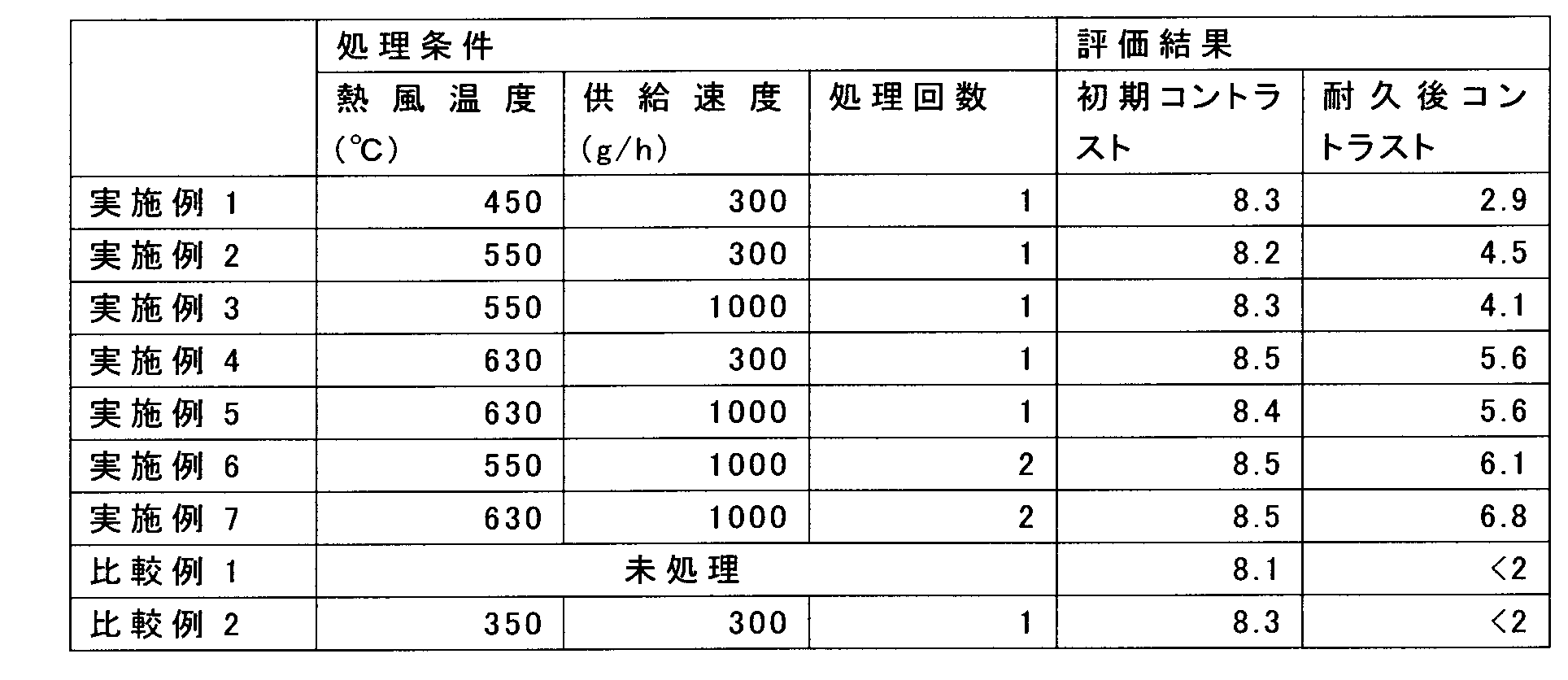
表2の結果から、実施例1~7の負帯電粒子は、比較例1、2の負帯電粒子よりも耐久後のコントラストの値が高く、表示性能が改善されていることが判る。
(5)情報表示用パネルの文字情報の表示性能評価
上述した(4)情報表示用パネルの表示性能評価で作製した実施例1~7および比較例1、2の情報表示用パネルとして、ドットマトリックス表示できるものを用いて、実際に「文字画像」を見た状況で目視判定した。
上述した(4)情報表示用パネルの表示性能評価で作製した実施例1~7および比較例1、2の情報表示用パネルとして、ドットマトリックス表示できるものを用いて、実際に「文字画像」を見た状況で目視判定した。
<コントラスト比評価法>
幅300μmのストライプ電極を対向直交交差させて形成した画素が100個×100個でマトリックス配置された構成の情報表示用パネルを評価用パネルとして作製して評価に用いた。正帯電性黒色粒子を含んだ粒子群と、負帯電性白色粒子を含んだ粒子群とをパネル基板間に当容量で、合わせて25%の体積占有率で封入し、チェッカー模様をテストパターンとして表示させ、白色表示部分の反射率および黒色表示部分の反射率を光学濃度計で測定子、白色表示部分の反射率と黒色表示部分の反射率との比をコントラスト比として鮮明な表示性の指標とした。
幅300μmのストライプ電極を対向直交交差させて形成した画素が100個×100個でマトリックス配置された構成の情報表示用パネルを評価用パネルとして作製して評価に用いた。正帯電性黒色粒子を含んだ粒子群と、負帯電性白色粒子を含んだ粒子群とをパネル基板間に当容量で、合わせて25%の体積占有率で封入し、チェッカー模様をテストパターンとして表示させ、白色表示部分の反射率および黒色表示部分の反射率を光学濃度計で測定子、白色表示部分の反射率と黒色表示部分の反射率との比をコントラスト比として鮮明な表示性の指標とした。
<視認性評価>
準備した評価用パネルを用いて、白地に黒表示として12ポイントサイズの文字情報を表示して、目視にてその見やすさを評価した。以下に評価結果を示す。
準備した評価用パネルを用いて、白地に黒表示として12ポイントサイズの文字情報を表示して、目視にてその見やすさを評価した。以下に評価結果を示す。
実施例1:耐久試験前に表示させた文字画像は非常に見やすかったが、耐久試験後に表示させた文字画像は見にくくなっていた。それでも実用上は問題ないと判断できるコントラストが得られていた。
実施例2~3:耐久試験前に表示させた文字画像は非常に見やすかったが、耐久試験後に表示させた文字画像はやや見にくくなっていた。それでも実用上はまったく問題ないコントラストが得られていた。
実施例4~7:耐久試験前に表示させた文字画像は非常に見やすく、耐久試験後に表示させた文字画像も見やすかった。耐久試験前も耐久試験後も良好なコントラストが得られていた。
比較例1~2:耐久試験前に表示させた文字画像は非常に見やすかったが、耐久試験後に表示させた文字画像は非常に見やすくなっていた。これでは実用上には問題ありと判断せざるを得ないコントラストであった。
実施例2~3:耐久試験前に表示させた文字画像は非常に見やすかったが、耐久試験後に表示させた文字画像はやや見にくくなっていた。それでも実用上はまったく問題ないコントラストが得られていた。
実施例4~7:耐久試験前に表示させた文字画像は非常に見やすく、耐久試験後に表示させた文字画像も見やすかった。耐久試験前も耐久試験後も良好なコントラストが得られていた。
比較例1~2:耐久試験前に表示させた文字画像は非常に見やすかったが、耐久試験後に表示させた文字画像は非常に見やすくなっていた。これでは実用上には問題ありと判断せざるを得ないコントラストであった。
本発明の対象となる情報表示用パネルは、ノートパソコン、PDA、携帯電話、ハンディターミナル等のモバイル機器の表示部、電子書籍、電子新聞等の電子ペーパー、看板、ポスター、黒板等の掲示板、電卓、家電製品、自動車用品等の表示部、ポイントカード、ICカード等のカード表示部、電子広告、電子POP、電子値札、電子棚札、電子楽譜、RF-ID機器の表示部の他、外部電界形成手段を用いて表示書き換えを行う表示部(いわゆるリライタブルペーパー)などに好適に用いられる。
Claims (4)
- 少なくとも一方が透明な対向する2枚の基板間に表示媒体を封入し、表示媒体を移動させて画像等の情報を表示する情報表示用パネルに用いる表示媒体を構成する表示媒体用粒子であって、樹脂を含む原料を混練、粉砕、分級することによって作製した粒子を熱処理によって球状化して得られた母粒子の表面に子粒子を付着又は固着させて得た複合型粒子からなることを特徴とする表示媒体用粒子。
- 請求項1記載の表示媒体用粒子において、前記母粒子の以下の式から得られる球状度が、0.950以上であることを特徴とする表示媒体用粒子;
球状度=粒子投影像と同面積の円の周囲長/粒子投影像の周囲長。 - 請求項1または2に記載の表示媒体用粒子を含んだ粒子群を表示媒体として用いたことを特徴とする情報表示用パネル。
- 少なくとも一方が透明な対向する2枚の基板間に表示媒体を封入し、表示媒体を移動させて画像等の情報を表示する情報表示用パネルに用いる表示媒体を構成する表示媒体用粒子の製造方法であって、樹脂を含む原料を混練、粉砕、分級することによって粒子を作製し、作製した粒子を熱処理によって球状化して母粒子を得、得られた母粒子の表面に子粒子を付着又は固着させることで複合型粒子からなる表示媒体粒子を得ることを特徴とする表示媒体用粒子の製造方法。
Priority Applications (1)
| Application Number | Priority Date | Filing Date | Title |
|---|---|---|---|
| JP2009554403A JPWO2009104752A1 (ja) | 2008-02-20 | 2009-02-20 | 表示媒体用粒子、それを用いた情報表示用パネルおよび表示媒体用粒子の製造方法 |
Applications Claiming Priority (2)
| Application Number | Priority Date | Filing Date | Title |
|---|---|---|---|
| JP2008038356 | 2008-02-20 | ||
| JP2008-038356 | 2008-02-20 |
Publications (1)
| Publication Number | Publication Date |
|---|---|
| WO2009104752A1 true WO2009104752A1 (ja) | 2009-08-27 |
Family
ID=40985629
Family Applications (1)
| Application Number | Title | Priority Date | Filing Date |
|---|---|---|---|
| PCT/JP2009/053069 Ceased WO2009104752A1 (ja) | 2008-02-20 | 2009-02-20 | 表示媒体用粒子、それを用いた情報表示用パネルおよび表示媒体用粒子の製造方法 |
Country Status (2)
| Country | Link |
|---|---|
| JP (1) | JPWO2009104752A1 (ja) |
| WO (1) | WO2009104752A1 (ja) |
Citations (2)
| Publication number | Priority date | Publication date | Assignee | Title |
|---|---|---|---|---|
| JP2006113267A (ja) * | 2004-10-14 | 2006-04-27 | Bridgestone Corp | 情報表示用パネルに用いる表示媒体用粒子 |
| JP2007240876A (ja) * | 2006-03-08 | 2007-09-20 | Fuji Xerox Co Ltd | 画像表示媒体 |
Family Cites Families (1)
| Publication number | Priority date | Publication date | Assignee | Title |
|---|---|---|---|---|
| US7426074B2 (en) * | 2006-05-19 | 2008-09-16 | Xerox Corporation | Electrophoretic display medium and display device |
-
2009
- 2009-02-20 WO PCT/JP2009/053069 patent/WO2009104752A1/ja not_active Ceased
- 2009-02-20 JP JP2009554403A patent/JPWO2009104752A1/ja active Pending
Patent Citations (2)
| Publication number | Priority date | Publication date | Assignee | Title |
|---|---|---|---|---|
| JP2006113267A (ja) * | 2004-10-14 | 2006-04-27 | Bridgestone Corp | 情報表示用パネルに用いる表示媒体用粒子 |
| JP2007240876A (ja) * | 2006-03-08 | 2007-09-20 | Fuji Xerox Co Ltd | 画像表示媒体 |
Also Published As
| Publication number | Publication date |
|---|---|
| JPWO2009104752A1 (ja) | 2011-06-23 |
Similar Documents
| Publication | Publication Date | Title |
|---|---|---|
| JP2007304409A (ja) | 表示媒体用粒子および情報表示用パネル | |
| JP4593675B2 (ja) | 表示媒体用粒子およびそれを用いた情報表示用パネル | |
| JP2007328329A (ja) | 表示媒体用粒子およびそれを用いた情報表示用パネル | |
| JP4925608B2 (ja) | 情報表示用パネル及び情報表示装置 | |
| JP5052104B2 (ja) | 表示媒体用粒子、情報表示用パネルおよび情報表示装置 | |
| WO2009104752A1 (ja) | 表示媒体用粒子、それを用いた情報表示用パネルおよび表示媒体用粒子の製造方法 | |
| JP2009139751A (ja) | 表示媒体用粒子およびそれを用いた情報表示用パネル | |
| JP2007298969A (ja) | 表示媒体用粒子およびそれを用いた情報表示用パネル | |
| JP2008185969A (ja) | 表示媒体用粒子及びこれを用いた情報表示用パネル | |
| JP5134775B2 (ja) | 表示媒体用粒子および情報表示用パネル | |
| JP2009133906A (ja) | 表示媒体用粒子およびそれを用いた情報表示用パネル | |
| JP4863762B2 (ja) | 表示媒体用粒子および情報表示用パネル | |
| JP2010276951A (ja) | 表示媒体用粒子、表示媒体用粒子の製造方法および情報表示用パネル | |
| JP2006313340A (ja) | 表示媒体用粒子及びそれを用いた情報表示用パネル | |
| WO2010137346A1 (ja) | 表示媒体用粒子およびこの表示媒体用粒子を用いた情報表示用パネル | |
| JP2009276431A (ja) | 表示媒体用粒子およびそれを用いた情報表示用パネル | |
| JP2009217180A (ja) | 表示媒体用粒子およびそれを用いた情報表示用パネル | |
| JP2006313329A (ja) | 表示媒体用粒子及びそれを用いた情報表示用パネル | |
| JP2008102231A (ja) | 表示媒体用粒子およびそれを用いた情報表示用パネル | |
| JP2006099046A (ja) | 表示媒体用粒子およびそれを用いた情報表示装置 | |
| JP2008139596A (ja) | 情報表示用パネル | |
| JP2009139742A (ja) | 表示媒体用粒子およびそれを用いた情報表示用パネル | |
| JP2009139736A (ja) | 表示媒体用粒子およびそれを用いた情報表示用パネル | |
| JP2007178855A (ja) | 表示媒体用粒子、その製造方法およびそれを用いた情報表示用パネル | |
| JP2010256723A (ja) | 光学的反射率および帯電性を有する粒子ならびに情報表示用パネル |
Legal Events
| Date | Code | Title | Description |
|---|---|---|---|
| 121 | Ep: the epo has been informed by wipo that ep was designated in this application |
Ref document number: 09711782 Country of ref document: EP Kind code of ref document: A1 |
|
| WWE | Wipo information: entry into national phase |
Ref document number: 2009554403 Country of ref document: JP |
|
| NENP | Non-entry into the national phase |
Ref country code: DE |
|
| 122 | Ep: pct application non-entry in european phase |
Ref document number: 09711782 Country of ref document: EP Kind code of ref document: A1 |