WO2009104239A1 - 不揮発性記憶装置及びその製造方法 - Google Patents
不揮発性記憶装置及びその製造方法 Download PDFInfo
- Publication number
- WO2009104239A1 WO2009104239A1 PCT/JP2008/052636 JP2008052636W WO2009104239A1 WO 2009104239 A1 WO2009104239 A1 WO 2009104239A1 JP 2008052636 W JP2008052636 W JP 2008052636W WO 2009104239 A1 WO2009104239 A1 WO 2009104239A1
- Authority
- WO
- WIPO (PCT)
- Prior art keywords
- layer
- memory device
- nonvolatile memory
- phase change
- wiring
- Prior art date
- Legal status (The legal status is an assumption and is not a legal conclusion. Google has not performed a legal analysis and makes no representation as to the accuracy of the status listed.)
- Ceased
Links
Images







Classifications
-
- H—ELECTRICITY
- H10—SEMICONDUCTOR DEVICES; ELECTRIC SOLID-STATE DEVICES NOT OTHERWISE PROVIDED FOR
- H10N—ELECTRIC SOLID-STATE DEVICES NOT OTHERWISE PROVIDED FOR
- H10N70/00—Solid-state devices having no potential barriers, and specially adapted for rectifying, amplifying, oscillating or switching
- H10N70/20—Multistable switching devices, e.g. memristors
- H10N70/231—Multistable switching devices, e.g. memristors based on solid-state phase change, e.g. between amorphous and crystalline phases, Ovshinsky effect
-
- H—ELECTRICITY
- H10—SEMICONDUCTOR DEVICES; ELECTRIC SOLID-STATE DEVICES NOT OTHERWISE PROVIDED FOR
- H10B—ELECTRONIC MEMORY DEVICES
- H10B63/00—Resistance change memory devices, e.g. resistive RAM [ReRAM] devices
- H10B63/20—Resistance change memory devices, e.g. resistive RAM [ReRAM] devices comprising selection components having two electrodes, e.g. diodes
-
- H—ELECTRICITY
- H10—SEMICONDUCTOR DEVICES; ELECTRIC SOLID-STATE DEVICES NOT OTHERWISE PROVIDED FOR
- H10B—ELECTRONIC MEMORY DEVICES
- H10B63/00—Resistance change memory devices, e.g. resistive RAM [ReRAM] devices
- H10B63/80—Arrangements comprising multiple bistable or multi-stable switching components of the same type on a plane parallel to the substrate, e.g. cross-point arrays
- H10B63/84—Arrangements comprising multiple bistable or multi-stable switching components of the same type on a plane parallel to the substrate, e.g. cross-point arrays arranged in a direction perpendicular to the substrate, e.g. 3D cell arrays
-
- H—ELECTRICITY
- H10—SEMICONDUCTOR DEVICES; ELECTRIC SOLID-STATE DEVICES NOT OTHERWISE PROVIDED FOR
- H10N—ELECTRIC SOLID-STATE DEVICES NOT OTHERWISE PROVIDED FOR
- H10N70/00—Solid-state devices having no potential barriers, and specially adapted for rectifying, amplifying, oscillating or switching
- H10N70/011—Manufacture or treatment of multistable switching devices
- H10N70/021—Formation of switching materials, e.g. deposition of layers
- H10N70/026—Formation of switching materials, e.g. deposition of layers by physical vapor deposition, e.g. sputtering
-
- H—ELECTRICITY
- H10—SEMICONDUCTOR DEVICES; ELECTRIC SOLID-STATE DEVICES NOT OTHERWISE PROVIDED FOR
- H10N—ELECTRIC SOLID-STATE DEVICES NOT OTHERWISE PROVIDED FOR
- H10N70/00—Solid-state devices having no potential barriers, and specially adapted for rectifying, amplifying, oscillating or switching
- H10N70/011—Manufacture or treatment of multistable switching devices
- H10N70/041—Modification of switching materials after formation, e.g. doping
-
- H—ELECTRICITY
- H10—SEMICONDUCTOR DEVICES; ELECTRIC SOLID-STATE DEVICES NOT OTHERWISE PROVIDED FOR
- H10N—ELECTRIC SOLID-STATE DEVICES NOT OTHERWISE PROVIDED FOR
- H10N70/00—Solid-state devices having no potential barriers, and specially adapted for rectifying, amplifying, oscillating or switching
- H10N70/011—Manufacture or treatment of multistable switching devices
- H10N70/041—Modification of switching materials after formation, e.g. doping
- H10N70/043—Modification of switching materials after formation, e.g. doping by implantation
-
- H—ELECTRICITY
- H10—SEMICONDUCTOR DEVICES; ELECTRIC SOLID-STATE DEVICES NOT OTHERWISE PROVIDED FOR
- H10N—ELECTRIC SOLID-STATE DEVICES NOT OTHERWISE PROVIDED FOR
- H10N70/00—Solid-state devices having no potential barriers, and specially adapted for rectifying, amplifying, oscillating or switching
- H10N70/011—Manufacture or treatment of multistable switching devices
- H10N70/041—Modification of switching materials after formation, e.g. doping
- H10N70/046—Modification of switching materials after formation, e.g. doping by diffusion, e.g. photo-dissolution
-
- H—ELECTRICITY
- H10—SEMICONDUCTOR DEVICES; ELECTRIC SOLID-STATE DEVICES NOT OTHERWISE PROVIDED FOR
- H10N—ELECTRIC SOLID-STATE DEVICES NOT OTHERWISE PROVIDED FOR
- H10N70/00—Solid-state devices having no potential barriers, and specially adapted for rectifying, amplifying, oscillating or switching
- H10N70/011—Manufacture or treatment of multistable switching devices
- H10N70/061—Shaping switching materials
- H10N70/063—Shaping switching materials by etching of pre-deposited switching material layers, e.g. lithography
-
- H—ELECTRICITY
- H10—SEMICONDUCTOR DEVICES; ELECTRIC SOLID-STATE DEVICES NOT OTHERWISE PROVIDED FOR
- H10N—ELECTRIC SOLID-STATE DEVICES NOT OTHERWISE PROVIDED FOR
- H10N70/00—Solid-state devices having no potential barriers, and specially adapted for rectifying, amplifying, oscillating or switching
- H10N70/801—Constructional details of multistable switching devices
- H10N70/821—Device geometry
- H10N70/826—Device geometry adapted for essentially vertical current flow, e.g. sandwich or pillar type devices
-
- H—ELECTRICITY
- H10—SEMICONDUCTOR DEVICES; ELECTRIC SOLID-STATE DEVICES NOT OTHERWISE PROVIDED FOR
- H10N—ELECTRIC SOLID-STATE DEVICES NOT OTHERWISE PROVIDED FOR
- H10N70/00—Solid-state devices having no potential barriers, and specially adapted for rectifying, amplifying, oscillating or switching
- H10N70/801—Constructional details of multistable switching devices
- H10N70/841—Electrodes
-
- H—ELECTRICITY
- H10—SEMICONDUCTOR DEVICES; ELECTRIC SOLID-STATE DEVICES NOT OTHERWISE PROVIDED FOR
- H10N—ELECTRIC SOLID-STATE DEVICES NOT OTHERWISE PROVIDED FOR
- H10N70/00—Solid-state devices having no potential barriers, and specially adapted for rectifying, amplifying, oscillating or switching
- H10N70/801—Constructional details of multistable switching devices
- H10N70/881—Switching materials
- H10N70/882—Compounds of sulfur, selenium or tellurium, e.g. chalcogenides
- H10N70/8828—Tellurides, e.g. GeSbTe
-
- G—PHYSICS
- G11—INFORMATION STORAGE
- G11C—STATIC STORES
- G11C13/00—Digital stores characterised by the use of storage elements not covered by groups G11C11/00, G11C23/00, or G11C25/00
- G11C13/0002—Digital stores characterised by the use of storage elements not covered by groups G11C11/00, G11C23/00, or G11C25/00 using resistive RAM [RRAM] elements
- G11C13/0004—Digital stores characterised by the use of storage elements not covered by groups G11C11/00, G11C23/00, or G11C25/00 using resistive RAM [RRAM] elements comprising amorphous/crystalline phase transition cells
-
- G—PHYSICS
- G11—INFORMATION STORAGE
- G11C—STATIC STORES
- G11C2213/00—Indexing scheme relating to G11C13/00 for features not covered by this group
- G11C2213/70—Resistive array aspects
- G11C2213/72—Array wherein the access device being a diode
-
- Y—GENERAL TAGGING OF NEW TECHNOLOGICAL DEVELOPMENTS; GENERAL TAGGING OF CROSS-SECTIONAL TECHNOLOGIES SPANNING OVER SEVERAL SECTIONS OF THE IPC; TECHNICAL SUBJECTS COVERED BY FORMER USPC CROSS-REFERENCE ART COLLECTIONS [XRACs] AND DIGESTS
- Y10—TECHNICAL SUBJECTS COVERED BY FORMER USPC
- Y10S—TECHNICAL SUBJECTS COVERED BY FORMER USPC CROSS-REFERENCE ART COLLECTIONS [XRACs] AND DIGESTS
- Y10S257/00—Active solid-state devices, e.g. transistors, solid-state diodes
- Y10S257/92—Conductor layers on different levels connected in parallel, e.g. to reduce resistance
-
- Y—GENERAL TAGGING OF NEW TECHNOLOGICAL DEVELOPMENTS; GENERAL TAGGING OF CROSS-SECTIONAL TECHNOLOGIES SPANNING OVER SEVERAL SECTIONS OF THE IPC; TECHNICAL SUBJECTS COVERED BY FORMER USPC CROSS-REFERENCE ART COLLECTIONS [XRACs] AND DIGESTS
- Y10—TECHNICAL SUBJECTS COVERED BY FORMER USPC
- Y10S—TECHNICAL SUBJECTS COVERED BY FORMER USPC CROSS-REFERENCE ART COLLECTIONS [XRACs] AND DIGESTS
- Y10S977/00—Nanotechnology
- Y10S977/70—Nanostructure
- Y10S977/701—Integrated with dissimilar structures on a common substrate
- Y10S977/712—Integrated with dissimilar structures on a common substrate formed from plural layers of nanosized material, e.g. stacked structures
-
- Y—GENERAL TAGGING OF NEW TECHNOLOGICAL DEVELOPMENTS; GENERAL TAGGING OF CROSS-SECTIONAL TECHNOLOGIES SPANNING OVER SEVERAL SECTIONS OF THE IPC; TECHNICAL SUBJECTS COVERED BY FORMER USPC CROSS-REFERENCE ART COLLECTIONS [XRACs] AND DIGESTS
- Y10—TECHNICAL SUBJECTS COVERED BY FORMER USPC
- Y10S—TECHNICAL SUBJECTS COVERED BY FORMER USPC CROSS-REFERENCE ART COLLECTIONS [XRACs] AND DIGESTS
- Y10S977/00—Nanotechnology
- Y10S977/70—Nanostructure
- Y10S977/734—Fullerenes, i.e. graphene-based structures, such as nanohorns, nanococoons, nanoscrolls or fullerene-like structures, e.g. WS2 or MoS2 chalcogenide nanotubes, planar C3N4, etc.
Definitions
- the present invention relates to a nonvolatile memory device and a method for manufacturing the same, and more particularly, to a nonvolatile memory including a phase change film including a material that changes between a crystalline state and an amorphous state by applying a voltage.
- the present invention relates to an apparatus and a manufacturing method thereof.
- NAND flash memory and small HDD have rapidly evolved in recording density and formed a large market.
- both the NAND flash memory and the small HDD are expected to face the limit of recording density in the future.
- the NAND flash memory uses a transistor for the storage portion, miniaturization is expected to reach the limit due to the so-called short channel effect.
- the “short channel effect” is a phenomenon that occurs when the distance between the source portion and the drain portion is reduced due to miniaturization of the device, and specific examples include an increase in leakage current between the source and the drain.
- the manufacturing cost is increased due to the reduction of the minimum line width.
- the tracking accuracy accuracy of aligning the head with the correct position of the track on the HDD is expected to reach its limit.
- phase change nonvolatile memory device uses a characteristic that a phase change film changes between a crystalline state and an amorphous state by applying an electric field pulse to a semiconductor film (phase change film) It is. By reversibly converting the high resistance state (amorphous state, on) and the low resistance state (crystalline state, off) in the phase change film, information can be rewritten and the power can be turned off. Information is stored so that it will not disappear. Since the high-resistance and low-resistance states of the phase change film are stable, non-volatility is realized.
- the phase change type nonvolatile memory device does not have a problem that may occur in the above-described NAND flash memory or small HDD, and is considered superior to the former two in terms of high speed and miniaturization.
- phase change type nonvolatile memory device since a relatively large current flows at the time of operation, particularly at the time of erasing (reset), reduction of this operating current is required.
- nitrogen, oxygen or carbon ions are doped in a semiconductor integrated circuit device using an alloy film (GST film) of germanium (Ge), antimony (Sb) and tellurium (Te) as a memory element.
- GST film germanium
- Sb antimony
- Te tellurium
- a specific example is that a region where oxygen ions of high concentration are implanted has almost insulating properties, and a current for rewriting and signal transmission is limited to a region where ions are implanted at a low concentration (patent) Reference 1).
- the present invention relates to a nonvolatile memory device including a phase change film including a material that changes between a crystalline state and an amorphous state by applying a voltage, and can reduce power consumption. And a method for manufacturing the same.
- the first layer, the second layer, and the first layer and the second layer are sandwiched between the first layer and the second layer.
- a recording layer capable of reversibly transitioning between a first state having a low resistance and a second state having a high resistance by a current supplied through the layer, wherein the recording layer includes a main layer In the plane of the surface, there is provided a non-volatile memory device having a first portion and a second portion having a relatively higher nitrogen content than the first portion.
- the resistance is caused by a current sandwiched between the first layer and the second layer and supplied through the first layer and the second layer.
- a method for manufacturing a nonvolatile memory device having a recording layer capable of reversibly transitioning between a low first state and a high resistance second state, the first layer and a recording layer containing nitrogen And a second layer, and a step of removing nitrogen from the side surface of the recording layer.
- a method for manufacturing a nonvolatile memory device is provided. .
- a resistance is obtained by a current sandwiched between the first layer and the second layer and supplied through the first layer and the second layer.
- a method for manufacturing a nonvolatile memory device having a recording layer capable of reversibly transitioning between a first state having a low resistance and a second state having a high resistance, wherein the first layer, the recording layer There is provided a method for manufacturing a nonvolatile memory device, comprising: a step of forming a stacked body including two layers; and a step of introducing nitrogen from a side surface of the recording layer.
- a resistance is obtained by a current sandwiched between the first layer and the second layer and supplied through the first layer and the second layer.
- a method for manufacturing a nonvolatile memory device is provided. That.
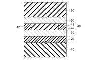
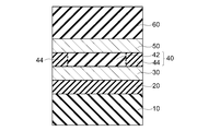
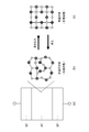
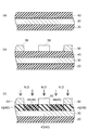
- FIG. 1 is a schematic cross-sectional view illustrating an example (specific example 1) of a nonvolatile memory device according to a first embodiment of the present invention. It is a schematic cross section showing another example (specific example 2) of the nonvolatile memory device according to the first embodiment of the present invention. It is a conceptual diagram for demonstrating the operation mechanism of the non-volatile memory device which concerns on this embodiment.
- (A) is a schematic cross-sectional view of the phase change film 40 for representing the effect of the specific example 1
- (b) is a schematic cross-sectional view of the phase change film 40 for representing the effect of the specific example 2.
- FIG. 6 is a schematic cross-sectional view of a phase change film 40 for explaining an effect of a specific example 2.
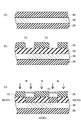
- FIG. 12 is a process cross-sectional view illustrating an example of a method for manufacturing the nonvolatile memory device in specific example 1.
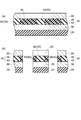
- FIG. 12 is a process cross-sectional view illustrating another example of the manufacturing method according to the nonvolatile memory device in specific example 1.
- FIG. 12 is a process cross-sectional view illustrating another example of the manufacturing method according to the nonvolatile memory device in specific example 1.
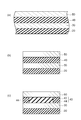
- FIG. 12 is a process cross-sectional view illustrating an example of a manufacturing method according to the nonvolatile memory device in specific example 2.
- FIG. 12 is a process cross-sectional view illustrating another example of the method for manufacturing the nonvolatile memory device in specific example 2.
- FIG. 12 is a process cross-sectional view illustrating another example of the method for manufacturing the nonvolatile memory device in specific example 2.
- FIG. It is a schematic diagram showing an example (specific example 3) of the nonvolatile memory device according to the third embodiment of the present invention.
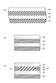
- 12 is a process cross-sectional view illustrating an example of a method for manufacturing the nonvolatile memory device in specific example 3.
- FIG. 12 is a process cross-sectional view illustrating another example of the manufacturing method according to the nonvolatile memory device in specific example 3.
- FIG. 12 is a process cross-sectional view illustrating another example of the manufacturing method according to the nonvolatile memory device in specific example 3.
- FIG. FIG. 9 is a schematic view illustrating a nonvolatile memory device according to a fifth embodiment of the invention.
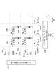
- FIG. 17 is a schematic diagram illustrating a circuit of the nonvolatile memory device illustrated in FIG. 16.
- nonvolatile memory device 2 nonvolatile memory device 2a first layer nonvolatile memory device 2b second layer nonvolatile memory device 4 nonvolatile memory device 6 nonvolatile memory device 10 first wiring 20 rectifying element 30 first electrode 40 phase change film 42 Low nitrogen concentration portion 44 High nitrogen concentration portion 46 Nitrogen oxygen introduction portion 48 Phase change material film 50 Second electrode 60 Second wiring 70 Dummy mask 105 Substrate 106 Main surface 110 First wiring 110a First first layer Wiring 110b second-layer first wiring 115 word line driver and decoder 120 second wiring 120a first-layer second wiring 120b second-layer second wiring 125 bit-line driver, decoder, and readout circuit 140 Rectifying element unit 140a Switch element unit 140b Switch element unit 200 Storage unit 200a First layer storage unit 200b Second layer storage unit
- FIG. 1 is a schematic cross-sectional view showing an example (specific example 1) of the nonvolatile memory device according to the first embodiment of the invention.
- the nonvolatile memory device of this specific example includes a first wiring 10, a rectifying element 20 provided on the first wiring 10, and a first electrode (first electrode provided on the rectifying element 20. Layer) 30, a phase change film (recording layer) 40 provided on the main surface of the first electrode 30, and a second electrode (second layer) provided on the main surface of the phase change film 40.
- the “main surface” means a surface perpendicular to the stacking direction (vertical direction in FIG. 1) of the first electrode 30, the phase change film 40, the second electrode 50, and the like.
- the phase change film 40 contains nitrogen in whole or in part, and a second portion (high nitrogen concentration portion 44) having a relatively high nitrogen concentration is formed inside the main surface, and the main surface.
- the first portion (low nitrogen concentration portion 42) having a relatively low nitrogen concentration is provided on the outside in the plane. That is, the low nitrogen concentration portion 42 is provided so as to surround the high nitrogen concentration portion 44 in the main surface.
- a heater layer made of a material having a resistivity of, for example, about 10 ⁇ 5 ⁇ cm or more is provided on the first electrode 30 side or the second electrode 50 side. (Not shown) may be provided.
- the rectifying element 20 is made of a diode, for example.
- the first electrode 30 and the second electrode 50 can be made of a material that is not easily oxidized in consideration of the case where the entire element is oxidized. Examples of such materials include the compounds listed below.
- MN M is at least one element selected from the group consisting of Ti, Zr, Hf, V, Nb, and Ta. N is nitrogen.
- MO x M is from the group of Ti, V, Cr, Mn, Fe, Co, Ni, Cu, Zr, Nb, Mo, Ru, Rh, Pd, Ag, Hf, Ta, W, Re, Ir, Os, and Pt. At least one element selected. x satisfies 1 ⁇ x ⁇ 4. O is oxygen.
- (C) AMO 3 A is at least one element selected from the group of La, K, Ca, Sr, Ba, and Ln (lanthanoid).
- M is from the group of Ti, V, Cr, Mn, Fe, Co, Ni, Cu, Zr, Nb, Mo, Ru, Rh, Pd, Ag, Hf, Ta, W, Re, Ir, Os, and Pt.
- At least one element selected. O is oxygen.
- a 2 MO 4 A is at least one element selected from the group of K, Ca, Sr, Ba, and Ln (lanthanoid).
- M is from the group of Ti, V, Cr, Mn, Fe, Co, Ni, Cu, Zr, Nb, Mo, Ru, Rh, Pd, Ag, Hf, Ta, W, Re, Ir, Os, and Pt.
- At least one element selected. O is oxygen.
- the phase change film 40 includes a material that changes between a crystalline state and an amorphous state by applying a voltage.
- this material include chalcogenide-based materials.
- Chalcogenide is a general term for compounds containing group 16 elements such as Se and Te, and is derived from the fact that group 16 elements are called chalcogens.
- Specific examples include those containing Se or Te, and more specifically, Ge 2 Sb 2 Te 5 , GeSbTe, SbTe, AsSbTe, SeSbTe, AgInSbTe, and the like.
- crystal does not mean a complete crystal but includes a single crystal and a polycrystal state including defects.
- amorphous does not mean only those having a completely disordered atomic arrangement, but those having a short-range periodic structure or containing fine crystal grains in a disordered matrix. Also included in “amorphous”.
- the phase change film 40 is produced by introducing nitrogen into all or part of the above materials.
- the purpose of introducing nitrogen is to stabilize the crystalline or amorphous state. When nitrogen is introduced, the phase change temperature rises, so that the phase change is less likely to occur. As a result, the recorded information is not easily erased, and non-volatility is ensured.
- the high nitrogen concentration portion 44 is a portion having a relatively high nitrogen concentration
- the low nitrogen concentration portion 42 is a portion having a relatively low nitrogen concentration.
- FIG. 2 is a schematic cross-sectional view showing another example (specific example 2) of the nonvolatile memory device according to the first embodiment of the invention.
- the nonvolatile memory device of this example includes a first wiring 10, a rectifying element 20 provided on the first wiring 10, a first electrode 30 provided on the rectifying element 20, Phase change film 40 provided on the main surface of one electrode 30, second electrode 50 provided on the main surface of phase change film 40, and provided on second electrode 50 A second wiring 60.
- the phase change film 40 contains nitrogen in whole or in part, and the first portion (low nitrogen concentration portion 42) having a relatively low nitrogen concentration is formed inside the main surface, and the main surface.
- the second portion (high nitrogen concentration portion 44) having a relatively high nitrogen concentration is provided on the outside in the plane. That is, the high nitrogen concentration portion 44 is provided so as to surround the low nitrogen concentration portion 42 in the main surface.
- a material having a resistivity of, for example, about 10 ⁇ 5 ⁇ cm or more is provided on the first electrode 30 side or the second electrode 50 side.
- a heater layer (not shown) may be provided.
- Constituent materials and the like of the rectifying element 20, the first electrode 30, the second electrode 50, and the phase change film 40 of this specific example can be the same as those described above regarding the specific example 1.
- Example 1 The difference from Example 1 is that the positional relationship between the high nitrogen concentration portion 44 and the low nitrogen concentration portion 42 is reversed. That is, in the specific example 1, the low nitrogen concentration portion 42 is disposed outside in the plane of the main surface, whereas in the specific example 2, the low nitrogen concentration portion 42 is disposed inside in the plane of the main surface.
- phase change film 40 has portions with different nitrogen concentrations in the main surface. Specific examples 1 and 2 both have this feature.
- FIG. 3 is a conceptual diagram for explaining an operation mechanism of the nonvolatile memory device according to the present embodiment.
- 3A is a schematic cross-sectional view showing the vicinity of the phase change film 40 of the nonvolatile memory device according to this embodiment.
- FIG. 3B is a schematic diagram showing a structure of an amorphous state of chalcogenide that can be a material of the phase change film 40, specifically, Ge 2 Sb 2 Te 5 .
- this compound has a structure composed of various rings such as a 4-membered ring, a 6-membered ring, and an 8-membered ring.
- FIG. 3 (c) is a schematic view illustrating the structure of the crystalline state of Ge 2 Sb 2 Te 5.
- this compound has a structure consisting of only a 4-membered ring, a 6-membered ring, and an 8-membered ring.
- a chalcogenide such as Ge 2 Sb 2 Te 5 used for the phase change film 40 undergoes a phase change when heat is applied, and changes between a low-resistance crystalline state and a high-resistance amorphous state.
- the amorphous state (FIG. 3B) is the initial state, and writing is performed when this changes to the crystalline state (FIG. 3C).
- the phase changes from the crystalline state (FIG. 3C) to the amorphous state (FIG. 3B) the written information is erased. It is also possible to adopt a system in which writing is performed when the crystalline state (FIG. 3C) is set to the initial state and the phase changes to the amorphous state (FIG. 3B).
- Recording (writing) of information in the phase change film 40 is performed by applying a voltage to the phase change film 40 and causing a current generation pulse to flow. Due to the Joule heat generated at this time, the phase change film 40 is heated to a temperature higher than the crystallization temperature. This temperature is maintained for a certain period of time, for example, less than 1 microsecond. Thereafter, the phase change film 40 is gradually cooled to change into a crystalline state. Thereby, information is written.
- phase change film 40 Information in the phase change film 40 is erased by applying a large current pulse to the phase change film 40 and using Joule heat generated at this time. Due to the Joule heat, the phase change film 40 is heated to a melting point (in the case of Ge 2 Sb 2 Te 5 , the melting point is 633 ° C.) or more. Thereafter, the phase change film 40 is rapidly cooled, for example, in a time shorter than 100 ns to change the phase to an amorphous state. Thereby, information is erased.
- a melting point in the case of Ge 2 Sb 2 Te 5 , the melting point is 633 ° C.
- Reproduction of information in the phase change film 40 is performed by applying a voltage to the phase change film 40 to flow a current pulse and detecting a resistance value.
- the current pulse has a minute amplitude such that the material forming the phase change film 40 does not cause a phase change.
- FIG. 4A is a schematic cross-sectional view of the phase change film 40 for representing the effect of the first specific example.
- the phase change film 40 has a high nitrogen concentration portion 44 inside on the main surface and a low nitrogen concentration portion 42 outside on the main surface.
- the resistivity of the low nitrogen concentration portion 42 is high nitrogen concentration regardless of whether the low nitrogen concentration portion 42 is in a crystalline state or an amorphous state. It becomes lower than the resistivity of the portion 44. Accordingly, it is possible to preferentially flow current through the low nitrogen concentration portion 42, and hardly flow current through the high nitrogen concentration portion 44. As a result, it is possible to cause a current to flow preferentially through the low nitrogen concentration portion 42 and change only the low nitrogen concentration portion 42.
- the phase of the low nitrogen concentration portion 42 In order to change the phase of the low nitrogen concentration portion 42 from the crystalline state to the amorphous state, it is necessary to melt the low nitrogen concentration portion 42. In this case as well, a current pulse is preferentially applied only to the low nitrogen concentration portion 42. It is possible to change the phase to an amorphous state by flowing and locally melting only the low nitrogen concentration portion and quenching. That is, it is possible to change the phase of the low nitrogen concentration portion 42 from the crystalline state to the amorphous state and to change the phase from the amorphous state to the crystalline state while the high nitrogen concentration portion 44 is fixed in the amorphous state. Is possible. When the low nitrogen concentration portion 42 is melted, the temperature of the adjacent high nitrogen concentration portion 44 may rise to some extent.
- phase change (crystallization) temperature increases with the amount of nitrogen introduced. That is, by increasing the crystallization temperature of the high nitrogen concentration portion 44, it is possible to suppress crystallization of the high nitrogen concentration portion 44 even when the adjacent low nitrogen concentration portion 42 is heated.
- the high nitrogen concentration portion 44 is fixed in an amorphous state (the phase change from the amorphous state to the crystalline state is not caused), and the low nitrogen concentration portion 42 is formed. Only a phase change can be caused. That is, current can flow only in the low nitrogen concentration portion 42, and current can be prevented from flowing in the high nitrogen concentration portion 44.
- the amount of current flowing through the phase change film 40 is reduced and the power consumption is reduced as compared with the conventional phase change film having a uniform nitrogen concentration. It is done.
- FIG. 4B is a schematic cross-sectional view of the phase change film 40 for illustrating the effect of the second specific example.
- current can flow only in the low nitrogen concentration portion 42 and current can not flow in the high nitrogen concentration portion 44. That is, the specific example 2 also has the effect of reducing the amount of current flowing through the phase change film 40 and reducing the power consumption, compared to a conventional phase change film having a uniform nitrogen concentration.
- FIG. 5 is a schematic cross-sectional view of the phase change film 40 for explaining the effect of the second specific example.
- a phase change is caused in the low nitrogen concentration portion 42, and information is written and erased. Therefore, for stable operation, the current resistance characteristics and phase change temperature of the low nitrogen concentration portion 42 need to be within a predetermined range. However, if impurities are mixed in the low nitrogen concentration portion 42, the electrical resistance and the phase change temperature may fluctuate, and predetermined operating characteristics may not be obtained.
- the high nitrogen concentration portion 44 in which high concentration nitrogen is introduced is provided outside the low nitrogen concentration portion 42.
- the high nitrogen concentration portion 44 into which nitrogen is introduced at a high concentration serves as a protective wall, and impurities are less likely to enter the low nitrogen concentration portion 42 from the outside such as the inter-element insulating film. That is, according to the second specific example, an effect of preventing impurities from entering the low nitrogen concentration portion 42 of the phase change film 40 is also obtained.
- the yield decreases due to impurities entering the low nitrogen concentration portion 42 during the manufacturing process of the nonvolatile memory device, or the manufactured nonvolatile memory device is repeatedly written and erased in various environments. Even in such a case, it is possible to prevent fluctuations in operating characteristics due to diffusion of impurities into the low nitrogen concentration portion 42, and to improve long-term reliability.
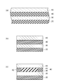
- FIG. 6 is a process cross-sectional view illustrating an example of a method for manufacturing the nonvolatile memory device according to the first specific example.
- the rectifying element 20 is formed on the first wiring 10 (not shown).
- a first electrode 30 is formed on the rectifying element 20.
- a phase change film 40 containing nitrogen is formed on the first electrode 30.
- a second electrode 50 is formed on the phase change film 40.
- a second wiring 60 (not shown) is formed on the second electrode 50.
- the stacked body is patterned by etching or the like. Etching is performed to the depth of the interface between the first wiring 10 and the rectifying element 20. Thereafter, as shown in FIG. 6C, nitrogen is removed from the side surface of the phase change film 40. Examples of the removal method include annealing under reduced pressure or under vacuum. The side surface of the phase change film 40 is damaged by the etching described above. When annealing is performed under reduced pressure or vacuum in this state, nitrogen near the side surface of the phase change film 40 is released. As a result, the nitrogen concentration is relatively low outside the main surface of the phase change film 40.
- the high nitrogen concentration portion 44 is formed inside the main surface, and the low nitrogen concentration portion 42 is formed outside the main surface. It is also effective to modify the phase change film 40 by exposing the side surface of the phase change film 40 to, for example, a rare gas plasma or irradiating with an ion beam or an electron beam before annealing. A physical or chemical impact is applied to the side surface of the phase change film 40 by plasma, an electron beam, or the like, thereby changing the bonding state of elements in the vicinity of the side surface or introducing defects. As a result, nitrogen desorption can be promoted.
- FIG. 7 and 8 are process cross-sectional views illustrating another example of the manufacturing method according to the nonvolatile memory device of specific example 1.
- FIG. 7A the rectifying element 20 is formed on the first wiring 10 (not shown).
- a first electrode 30 is formed on the rectifying element 20.
- a phase change material film 48 not containing nitrogen is formed on the first electrode 30.
- a dummy mask 70 is formed on the phase change material film 48.
- nitrogen is introduced into the phase change material film 48 using the dummy mask 70 as a mask.
- the introduction method include an ion implantation method, a gas phase diffusion method, and a method using nitrogen plasma or nitrogen radical.
- the nonvolatile memory device according to the first specific example having the high nitrogen concentration portion 44 inside the main surface and the low nitrogen concentration portion 42 outside the main surface is manufactured.
- FIG. 9 is a process cross-sectional view illustrating an example of a manufacturing method according to the nonvolatile memory device of specific example 2.
- the rectifying element 20 is formed on the first wiring 10 (not shown).
- a first electrode 30 is formed on the rectifying element 20.
- a phase change film 40 containing nitrogen is formed on the first electrode 30.
- nitrogen is introduced by sputtering in a nitrogen atmosphere having a flow rate ratio (N 2 / Ar) of nitrogen gas to argon gas of 1 to 10%. be able to.
- a second electrode 50 is formed on the phase change film 40.
- a second wiring 60 (not shown) is formed on the second electrode 50.
- phase change film 40 is formed from the side surface of the phase change film 40.
- the introduction method include annealing in an atmosphere containing nitrogen gas, and exposure to nitrogen plasma, nitrogen radicals, and the like.
- the nitrogen concentration is relatively high.
- an inner low nitrogen concentration portion 42 within the main surface is formed, and a high nitrogen concentration portion 44 is formed outside the main surface.
- elements other than the phase change film 40 can be nitrided together.
- nitrogen may be introduced into the rectifying element 20 to obtain a predetermined rectifying characteristic.
- FIG. 10A the rectifying element 20 is formed on the first wiring 10 (not shown).
- a first electrode 30 is formed on the rectifying element 20.
- a phase change material film 48 not containing nitrogen is formed on the first electrode 30.
- a dummy mask 70 is formed on the phase change material film 48.
- nitrogen is introduced into the phase change material film 48 using the dummy mask 70 as a mask. Examples of the introduction method include ion implantation. As a result, a phase change film 40 having a high nitrogen concentration portion 44 having a relatively high nitrogen concentration and a low nitrogen concentration portion 42 having a relatively low nitrogen concentration is formed.
- the phase change film 40 has the low nitrogen concentration portion 42 on the inner side in the plane of the main surface and the high nitrogen concentration portion 44 on the outer side in the plane of the main surface. Is produced.
- phase change film 40 containing nitrogen is formed on the first electrode 30 in the step according to FIG. 9A, but the phase change material film 48 containing no nitrogen is formed. Also good.
- the phase change material film 48 that does not contain nitrogen is formed on the first electrode 30 in the steps according to FIGS. 7A and 10A.
- the phase change film 40 may be formed.
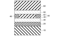
- FIG. 12 is a schematic cross-sectional view showing an example (specific example 3) of the nonvolatile memory device according to the third embodiment of the invention.
- the nonvolatile memory device of this example includes a first wiring 10, a rectifying element 20 provided on the first wiring 10, a first electrode 30 provided on the rectifying element 20, A phase change film 40 provided on one electrode 30; a second electrode 50 provided on the phase change film 40; and a second wiring 60 provided on the second electrode 50; .
- the phase change film 40 contains nitrogen in part or in part and oxygen in part, and a portion containing nitrogen at a relatively low concentration inside and not containing oxygen in the plane of the main surface ( It has a low nitrogen concentration portion 42), and a portion containing nitrogen at a relatively high concentration and containing oxygen (nitrogen oxygen introduction portion 46) outside the main surface.
- phase change film 40 in order to efficiently heat the phase change film 40 during the erase operation, for example, a resistivity of about 10 ⁇ 5 ⁇ cm or more is provided on the first electrode 30 side or the second electrode 50 side.
- a heater layer (not shown) made of the above material may be provided.
- the constituent materials of the rectifying element 20, the first electrode 30, the second electrode 50, and the phase change film 40 can be the same as those described above with respect to the first embodiment.
- phase change film 40 contains oxygen partially (outside in the main surface).
- Specific Example 3 can be the same as Specific Example 2 except that oxygen is introduced outside in the plane of the main surface of phase change film 40.
- phase change nonvolatile memory device by using the nitrogen concentration distribution in the in-plane direction of the main surface of the phase change film 40, power consumption is reduced and protection against impurities intrusion is achieved. A wall effect is obtained.
- oxygen is introduced into the phase change film 40 in addition to nitrogen.
- this example also has an effect of reducing the amount of current flowing through the phase change film 40 and reducing power consumption.
- the resistivity and phase change temperature of the nitrogen oxygen introduction portion 46 can be made higher than the resistivity and phase change temperature of the high nitrogen concentration portion 44 in the case of the specific example 2. .
- the effect of reducing power consumption is further increased.
- the current flowing through the nitrogen-oxygen introduction portion 46 can be further suppressed, and crystallization can be further suppressed.
- the phase of the low nitrogen concentration portion 42 can be stably changed, and the allowable range of current conditions for writing, erasing, and reading can be expanded.
- the nitrogen / oxygen introduction portion 46 serves as a protective wall, and the effect can be equal to or higher than the second specific example.
- FIG. 13 is a process cross-sectional view illustrating an example of a method for manufacturing the nonvolatile memory device according to the third specific example.
- the rectifying element 20 is formed on the first wiring 10 (not shown).
- a first electrode 30 is formed on the rectifying element 20.
- a phase change film 40 containing nitrogen is formed on the first electrode 30.
- nitrogen is introduced by sputtering in a nitrogen atmosphere having a flow rate ratio (N 2 / Ar) of nitrogen gas to argon gas of 1 to 10%. be able to.
- a second electrode 50 is formed on the phase change film 40.
- a second wiring 60 (not shown) is formed on the second electrode 50.
- patterning is performed by etching or the like. Etching is performed to the depth of the interface between the first wiring 10 and the rectifying element 20.
- nitrogen and oxygen are introduced from the side surface of the phase change film 40. Examples of the introduction method include nitriding treatment and oxidation treatment for the entire element including the first wiring 10 and the second wiring 60.
- the order of introducing nitrogen and oxygen does not matter. First, oxygen may be introduced after introducing nitrogen, nitrogen may be introduced after introducing oxygen, or both may be introduced simultaneously.
- the oxidation treatment may be annealing in an atmosphere containing oxygen, oxygen plasma treatment, or oxygen radical treatment. Further, this oxidation treatment may be used in combination with an oxidation treatment performed for repairing the rectifying element 20 damaged by patterning.
- the rectifying device 20 the use of CuInO 2, ZnInO 2 such oxides diode, the side wall portion of the rectifying element 20 in the patterning process shown in FIG. 13 (b) may be damaged.
- oxidation treatment can be performed to repair the damaged side wall portion of the rectifying element 20. Oxygen can be introduced from the side surface of the phase change film 40 during the oxidation treatment for repairing the rectifying element 20.
- the nitrogen concentration is relatively increased and oxygen is introduced outside the main surface of the phase change film 40.
- the low nitrogen concentration portion 42 is formed inside the main surface, and the nitrogen-oxygen introduction portion 46 is formed outside the main surface.
- FIG. 14 and 15 are process cross-sectional views illustrating another example of the manufacturing method according to the nonvolatile memory device of specific example 3.
- the rectifying element 20 is formed on the first wiring 10 (not shown).
- a first electrode 30 is formed on the rectifying element 20.
- a phase change film 40 containing nitrogen is formed on the first electrode 30.
- nitrogen is introduced by sputtering in a nitrogen atmosphere having a flow rate ratio (N 2 / Ar) of nitrogen gas to argon gas of 1 to 10%. Can do.
- a dummy mask 70 is formed on the phase change film 40.
- nitrogen and oxygen are introduced into the phase change film 40 using the dummy mask 70 as a mask.
- the introduction method include an ion implantation method, a gas phase diffusion method, a method using plasma and radicals, and the like.
- the order of introducing nitrogen and oxygen does not matter. First, oxygen may be introduced after introducing nitrogen, nitrogen may be introduced after introducing oxygen, or both may be introduced simultaneously.
- a nitrogen-oxygen-introducing portion 46 into which oxygen is introduced with a relatively high nitrogen concentration and a low nitrogen concentration portion 42 with a relatively low nitrogen concentration are formed.
- the dummy mask 70 is removed. Thereafter, the second electrode 50 is formed on the phase change film 40. Thereafter, a second wiring 60 (not shown) is formed on the second electrode 50.
- phase change film 40 has the low nitrogen concentration portion 42 on the inner side in the plane of the main surface and the nitrogen oxygen introduction portion 46 on the outer side in the plane of the main surface. Is produced.
- the phase change film 40 containing nitrogen is formed on the first electrode 30 in the steps shown in FIGS. 13A and 14A.
- the phase change material does not contain nitrogen.
- the film 48 may be formed.
- FIG. 16 is a schematic view illustrating a nonvolatile memory device according to the fifth embodiment of the invention.
- the inter-element isolation insulating film is omitted.
- a strip-shaped first wiring 110 extending in the X-axis direction is provided on the main surface 106 of the substrate 105.
- a band-like second wiring 120 extending in the Y-axis direction orthogonal to the X-axis in a plane parallel to the substrate 105 is provided to face the first wiring 110.
- a storage unit 200 made of a phase change film is sandwiched between the first wiring 110 and the second wiring 120. That is, in the nonvolatile memory device 2, the storage unit 200 is provided at a portion (cross point) where the first wiring 110 and the second wiring 120 intersect. This is a so-called cross-point cell array structure.
- the voltage applied to each storage unit 200 changes depending on the combination of the potential applied to the first wiring 110 and the potential applied to the second wiring 120, and the characteristics of the storage unit 200 at that time, that is, the resistance value (amorphous) Information can be stored or erased depending on the state of the high resistance state or the low resistance state of the crystalline state.
- a rectifying element unit 140 made of, for example, a diode is provided. be able to.
- FIG. 16 illustrates an example in which the rectifying element unit 140 is provided between the first wiring 110 and the storage unit 200, but the rectifying element unit 140 is provided between the second wiring 120 and the storage unit 200. It may be provided. Further, the rectifying element portion 140 may be provided in a region other than a region where the first wiring 110 and the second wiring 120 face each other.
- An electrode (not shown) can be provided between the rectifying element unit 140 and the storage unit 200 and between the storage unit 200 and the second wiring 120. This electrode also serves as a protective film.
- One storage section 200 (and rectifying element section 140) provided in a region where one first wiring 110 and one second wiring 120 cross each other is one element, which is referred to as a “cell”.
- the storage unit 200 made of a phase change film can have a low nitrogen concentration portion and a high nitrogen concentration portion in the in-plane direction of the main surface.
- the nonvolatile memory device of this embodiment has the effect described in the description of the first embodiment, that is, the effect of a protective wall against the reduction of power consumption and the entry of impurities.
- the storage unit 200 made of a phase change film can have a low nitrogen concentration portion and a nitrogen oxygen introduction portion in the main surface direction.
- the nonvolatile memory device of this embodiment has the effects described in the description of the third embodiment, that is, the effect of a protective wall against the reduction of power consumption and the entry of impurities.
- FIG. 16 illustrates an example in which three first wirings 110 and three second wirings 120 are provided, but the present invention is not limited to this, and the first wiring 110 and the second wiring 120 are not limited thereto.
- the number of wirings 120 is arbitrary.
- the first wiring 110 is referred to as a bit wiring (BL), and the second wiring 120 is referred to as a word line (WL).
- the first wiring 110 may be a word line (WL) and the second wiring 120 may be a bit line (BL).
- FIG. 17 is a schematic perspective view illustrating another example of the configuration of the nonvolatile memory device according to the fifth embodiment of the present invention.
- the memory unit 200 has a two-layer structure. That is, the nonvolatile memory device 4 is provided to face the substrate 105, the first wiring 110a in the first layer provided on the main surface 106 of the substrate 105, and the first wiring 110a in the first layer. A first-layer second wiring 120a, and a first-layer storage portion 200a sandwiched between the first-layer first wiring 110a and the first-layer second wiring 120a. These become the first-layer nonvolatile memory device 2a.
- the second wiring 120a in the first layer is used as the first wiring 110b in the second layer, the second layer storage unit 200b is provided thereon, and the second wiring 120b in the second layer is provided thereon. Is provided. These become the second-layer nonvolatile memory device 2b. Each layer is provided with switch element portions 140a and 140b.
- the storage unit 200 formed of each phase change film may have a low nitrogen concentration portion and a high nitrogen concentration portion, or a low nitrogen concentration portion and a nitrogen oxygen introduction portion.
- each effect mentioned above regarding FIG. 16 is acquired.
- the second wiring 120 a in the first layer and the first wiring 110 b in the second layer are respectively It is provided separately.
- the storage unit 200 made of the respective phase change films can have a low nitrogen concentration portion and a high nitrogen concentration portion, or a low nitrogen concentration portion and a nitrogen oxygen introduction portion. Also in this case, the effects described above with reference to FIG. 16 can be obtained.
- FIG. 17 and 18 illustrate the case where the storage unit 200 is stacked in two layers, three or more layers may be used.
- recording, erasing, and reproducing operations of the nonvolatile memory device according to the third embodiment of the present invention will be described with reference to FIG.
- the initial state (state in which no information is stored) of the storage unit 200 may be either a crystalline state (low resistance state) or an amorphous state (high resistance state).
- a case where the initial state of the storage unit 200 is an amorphous state (high resistance state) will be taken up.
- Recording (writing) of information in the storage unit 200 is performed by applying a voltage to the storage unit 200 and flowing a current pulse. For this reason, for example, a state in which the potential of the first wiring 110 is relatively lower than the potential of the second wiring 120 is created. If the second wiring 120 is set to a ground potential, for example, a negative potential may be applied to the first wiring 110. At this time, the current pulse preferentially flows through the low nitrogen concentration portion 42 described above.
- the low nitrogen concentration portion 42 of the storage unit 200 is heated to a temperature higher than the crystallization temperature due to Joule heat generated at this time. This temperature is maintained for a certain period of time, for example, less than 1 microsecond. Then, the memory
- all the first wirings 110 and all the second wirings 120 be precharged immediately before recording (writing) (during standby). Precharging is to keep the potential of each wiring constant in order to ensure good operating characteristics.
- the voltage pulse for recording may be generated by making the potential of the first wiring 110 higher than the potential of the second wiring 120.
- Erasing is performed by applying a large current pulse to the storage unit 200 and using Joule heat generated at this time. Also at this time, a current pulse preferentially flows through the low nitrogen concentration portion 42. Due to this Joule heat, the low nitrogen concentration portion 42 of the storage unit 200 is heated to a melting point (in the case of Ge 2 Sb 2 Te 5 , the melting point is 633 ° C.) or more. Thereafter, the storage unit 200 is rapidly cooled, for example, in a time shorter than 100 ns, and the phase of the low nitrogen concentration portion 42 is changed to an amorphous state. Thereby, information is erased. At this time, almost no current flows in the high nitrogen concentration portion 44 adjacent to the low nitrogen concentration portion 42 and the crystallization temperature is high. Therefore, when the low nitrogen concentration portion 42 is rapidly cooled after heating, it melts. And crystallization can be prevented.
- Reproduction is performed by applying a voltage to the storage unit 200 to flow a current pulse and detecting the resistance value at this time.
- the voltage pulse has a minute amplitude such that the material constituting the storage unit 200 does not cause a phase change.
- the resistance value of the storage unit 200 can be measured using a reading circuit.
- the read current generated from the read circuit flows to the storage unit 200 through the second wiring 120, and the resistance value of the storage unit 200 is measured by the read circuit.
- the low nitrogen concentration portion 42 is made crystalline or amorphous by writing / erasing, while the high nitrogen concentration portion 44 is always maintained in an amorphous state. Therefore, information can be reproduced by detecting a change in the resistance of the low nitrogen concentration portion 42.
- a current pulse can be preferentially passed through the low nitrogen concentration portion 42, and almost no current can be passed through the high nitrogen concentration portion 44. As a result, power consumption can be reduced.
- Such a non-volatile memory device can realize higher recording density and lower power consumption than conventional non-volatile memory devices using currently used hard disks and transistors.
- FIG. 19 is a schematic diagram illustrating a circuit of the nonvolatile memory device illustrated in FIG. 16.
- BL represents a bit line
- WL represents a word line.
- the word lines WL i ⁇ 1 , WL i , WL i + 1 extend in the X direction
- the bit lines BL j ⁇ 1 , BL j , BL j + 1 extend in the Y direction.
- each of the word lines WL i ⁇ 1 , WL i , WL i + 1 is connected to a word line driver and decoder 115 via a MOS transistor RSW (Row Switch) as a selection switch, and a bit line BL j ⁇ 1 , BL j, one end of the BL j + 1 is, MOS transistor CSW as a selection switch (column switch: column switch) bit line driver via is connected decoder, and read circuit 125.
- MOS transistor RSW Row Switch
- Selection signals R i ⁇ 1 , R i , and R i + 1 for selecting one word line (Row) are input to the gate of the MOS transistor RSW, and 1 to the gate of the MOS transistor CSW.
- Selection signals C j ⁇ 1 , C j , and C j + 1 for selecting one bit line (Column: column) are input.
- the storage unit 200, the word lines WL i-1, WL i, WL i + 1 and the bit lines BL j-1, BL j, are arranged in the intersection of BL j + 1.
- a rectifying element unit 140 is added to the storage unit 200.
- the cross-point type nonvolatile memory device of this specific example does not require individual connection of a MOS transistor to the memory portion of each cell and can be multi-layered. It is advantageous.
- a nonvolatile memory device including a phase change film containing a material that changes between a crystalline state and an amorphous state by applying a voltage
- the nonvolatile power consumption can be reduced.
- a storage device and a manufacturing method thereof are provided.
Landscapes
- Engineering & Computer Science (AREA)
- Manufacturing & Machinery (AREA)
- Semiconductor Memories (AREA)
Abstract
第1の層と、第2の層と、前記第1の層と前記第2の層との間に狭持され、前記第1の層と前記第2の層とを介して供給される電流により、抵抗が低い第1の状態と抵抗が高い第2の状態との間を可逆的に遷移可能な記録層と、を備え、前記記録層は、その主面の面内において、第1の部分と、前記第1の部分より窒素の含有量が相対的に高い第2の部分と、を有することを特徴とする不揮発性記憶装置が提供される。低消費電力の不揮発性の情報記録再生装置が提供される。
Description
本発明は、不揮発性記憶装置及びその製造方法に関し、より詳細には、電圧を印加することによって結晶状態と非晶質状態との間で変化する材料を含む相変化膜を備えた不揮発性記憶装置及びその製造方法に関する。
ユビキタス社会の実現に向け小型携帯機器の普及が進む中、近年、小型大容量の不揮発性記憶装置(メモリ)の需要が急速に増加している。とりわけ、NAND型フラッシュメモリ及び小型HDD(Hard Disk Drive)は、急速な記録密度の進化を遂げ、大きな市場を形成するに至っている。
しかしながら、NAND型フラッシュメモリ及び小型HDDは、ともに将来、記録密度の限界に直面することが予想される。
しかしながら、NAND型フラッシュメモリ及び小型HDDは、ともに将来、記録密度の限界に直面することが予想される。
NAND型フラッシュメモリについては、記憶部にトランジスタを用いているため、いわゆる短チャネル効果の影響により、微細化が限界に達することが予想される。「短チャネル効果」とは、装置の微細化によってソース部とドレイン部との距離が近くなることによって生ずる現象であり、具体例にはソースとドレインとの間のリーク電流の増加等である。また、最小線幅の縮小による製造コストの増大が生じている。
小型HDDについては、トラッキング精度(HDD上のトラックの正しい位置にヘッドを合わせることの精度)が限界に達することが予想される。
小型HDDについては、トラッキング精度(HDD上のトラックの正しい位置にヘッドを合わせることの精度)が限界に達することが予想される。
このため、記録密度の限界を打破する新規技術の開発が求められている。
このような新規技術として、相変化型不揮発性記憶装置(相変化メモリ)(PCRAM:Phase-Change Random Access Memory)が検討されている。相変化型不揮発性記憶装置は、半導体膜(相変化膜)に電界パルスを印加することによって相変化膜が結晶状態と非晶質状態との間で変化するという特性を利用する不揮発性記憶装置である。相変化膜において高抵抗状態(非晶質状態、オン)と低抵抗状態(結晶状態、オフ)とを可逆的に変換することによって、情報が書き換え可能なように、かつ、電源を切っても情報が消えないように記憶される。相変化膜の高抵抗及び低抵抗の状態がそれぞれ安定であるため、不揮発性が実現される。相変化型不揮発性記憶装置は、上述したNAND型フラッシュメモリや小型HDDにおいて生じ得る問題がなく、高速性及び微細化可能性において前二者より優れていると考えられる。
このような新規技術として、相変化型不揮発性記憶装置(相変化メモリ)(PCRAM:Phase-Change Random Access Memory)が検討されている。相変化型不揮発性記憶装置は、半導体膜(相変化膜)に電界パルスを印加することによって相変化膜が結晶状態と非晶質状態との間で変化するという特性を利用する不揮発性記憶装置である。相変化膜において高抵抗状態(非晶質状態、オン)と低抵抗状態(結晶状態、オフ)とを可逆的に変換することによって、情報が書き換え可能なように、かつ、電源を切っても情報が消えないように記憶される。相変化膜の高抵抗及び低抵抗の状態がそれぞれ安定であるため、不揮発性が実現される。相変化型不揮発性記憶装置は、上述したNAND型フラッシュメモリや小型HDDにおいて生じ得る問題がなく、高速性及び微細化可能性において前二者より優れていると考えられる。
ここで、相変化型不揮発性記憶装置については、動作時、特に消去(リセット)時において比較的大きな電流が流れることから、この動作電流の低減化が求められている。
これに関連する従来技術としては、ゲルマニウム(Ge)、アンチモン(Sb)そしてテルル(Te)の合金膜(GST膜)を記憶素子とした半導体集積回路装置において、窒素、酸素あるいは炭素のイオンをドーピングした半導体集積回路装置がある。具体例には、高濃度の酸素イオンを打ち込んだ領域は、ほとんど絶縁性を示し、書き換えや信号伝達のための電流は、その通路が低濃度イオン打ち込み領域に限定されるというものである(特許文献1)。
特開2006-156886号公報
本発明は、電圧を印加することによって結晶状態と非晶質状態との間で変化する材料を含む相変化膜を備えた不揮発性記憶装置において、消費電力を低減することができる不揮発性記憶装置及びその製造方法を提供する。
本発明の一態様によれば、第1の層と、第2の層と、前記第1の層と前記第2の層との間に狭持され、前記第1の層と前記第2の層とを介して供給される電流により、抵抗が低い第1の状態と抵抗が高い第2の状態との間を可逆的に遷移可能な記録層と、を備え、前記記録層は、その主面の面内において、第1の部分と、前記第1の部分より窒素の含有量が相対的に高い第2の部分と、を有することを特徴とする不揮発性記憶装置が提供される。
本発明の他の一態様によれば、第1の層と第2の層の間に狭持され、前記第1の層と前記第2の層とを介して供給される電流により、抵抗が低い第1の状態と抵抗が高い第2の状態との間を可逆的に遷移可能な記録層を有する不揮発性記憶装置の製造方法であって、第1の層と、窒素を含有する記録層と、第2の層と、を含む積層体を形成する工程と、前記記録層の側面から窒素を除去する工程と、を備えたことを特徴とする不揮発性記憶装置の製造方法が提供される。
本発明のさらに他の一態様によれば、第1の層と第2の層の間に狭持され、前記第1の層と前記第2の層とを介して供給される電流により、抵抗が低い第1の状態と抵抗が高い第2の状態との間を可逆的に遷移可能な記録層を有する不揮発性記憶装置の製造方法であって、第1の層と、記録層と、第2の層と、を含む積層体を形成する工程と、前記記録層の側面から窒素を導入する工程と、を備えたことを特徴とする不揮発性記憶装置の製造方法が提供される。
本発明のさらに他の一態様によれば、第1の層と第2の層の間に狭持され、前記第1の層と前記第2の層とを介して供給される電流により、抵抗が低い第1の状態と抵抗が高い第2の状態との間を可逆的に遷移可能な記録層を有する不揮発性記憶装置の製造方法であって、前記第1の層の上に前記記録層を形成する工程と、前記記録層の主面上にマスクを形成する工程と、前記記録層のうちで前記マスクにより覆われていない部分に相対的に高い濃度で窒素を導入する工程と、前記記録層の上に前記第2の層を形成する工程と、前記マスクにより覆われた部分と覆われていない部分と、を含むように、前記第1の層、前記記録層及び前記第2の層をパターニングする工程と、を備えたことを特徴とする不揮発性記憶装置の製造方法が提供される。
2 不揮発性記憶装置
2a 1層目の不揮発性記憶装置
2b 2層目の不揮発性記憶装置
4 不揮発性記憶装置
6 不揮発性記憶装置
10 第1の配線
20 整流素子
30 第1の電極
40 相変化膜
42 低窒素濃度部分
44 高窒素濃度部分
46 窒素酸素導入部分
48 相変化材料膜
50 第2の電極
60 第2の配線
70 ダミーマスク
105 基板
106 主面
110 第1の配線
110a 1層目の第1の配線
110b 2層目の第1の配線
115 ワード線ドライバ及びデコーダ
120 第2の配線
120a 1層目の第2の配線
120b 2層目の第2の配線
125 ビット線ドライバ、デコーダ、及び読出し回路
140 整流素子部
140a スイッチ素子部
140b スイッチ素子部
200 記憶部
200a 1層目の記憶部
200b 2層目の記憶部
2a 1層目の不揮発性記憶装置
2b 2層目の不揮発性記憶装置
4 不揮発性記憶装置
6 不揮発性記憶装置
10 第1の配線
20 整流素子
30 第1の電極
40 相変化膜
42 低窒素濃度部分
44 高窒素濃度部分
46 窒素酸素導入部分
48 相変化材料膜
50 第2の電極
60 第2の配線
70 ダミーマスク
105 基板
106 主面
110 第1の配線
110a 1層目の第1の配線
110b 2層目の第1の配線
115 ワード線ドライバ及びデコーダ
120 第2の配線
120a 1層目の第2の配線
120b 2層目の第2の配線
125 ビット線ドライバ、デコーダ、及び読出し回路
140 整流素子部
140a スイッチ素子部
140b スイッチ素子部
200 記憶部
200a 1層目の記憶部
200b 2層目の記憶部
以下、本発明の実施形態について図面を参照しつつ説明する。なお、各図面中、同様の構成要素には同一の符号を付して詳細な説明は適宜省略する。
(第1の実施形態)
図1は、本発明の第1の実施形態に係る不揮発性記憶装置の一例(具体例1)を表す模式断面図である。
本具体例の不揮発性記憶装置は、第1の配線10と、第1の配線10の上に設けられた整流素子20と、整流素子20の上に設けられた第1の電極(第1の層)30と、第1の電極30の主面の上に設けられた相変化膜(記録層)40と、相変化膜40の主面の上に設けられた第2の電極(第2の層)50と、第2の電極50の上に設けられた第2の配線60と、を備える。ここで、「主面」とは、第1の電極30や、相変化膜40、第2の電極50などの積層方向(図1において上下方向)に対して垂直な面をいう。ここで、相変化膜40は、全部または一部に窒素を含有し、主面の面内において内側に相対的に窒素濃度の高い第2の部分(高窒素濃度部分44)を、また主面の面内において外側に相対的に窒素濃度の低い第1の部分(低窒素濃度部分42)を有する。すなわち、低窒素濃度部分42は、主面の面内において高窒素濃度部分44を取り囲むように設けられている。
(第1の実施形態)
図1は、本発明の第1の実施形態に係る不揮発性記憶装置の一例(具体例1)を表す模式断面図である。
本具体例の不揮発性記憶装置は、第1の配線10と、第1の配線10の上に設けられた整流素子20と、整流素子20の上に設けられた第1の電極(第1の層)30と、第1の電極30の主面の上に設けられた相変化膜(記録層)40と、相変化膜40の主面の上に設けられた第2の電極(第2の層)50と、第2の電極50の上に設けられた第2の配線60と、を備える。ここで、「主面」とは、第1の電極30や、相変化膜40、第2の電極50などの積層方向(図1において上下方向)に対して垂直な面をいう。ここで、相変化膜40は、全部または一部に窒素を含有し、主面の面内において内側に相対的に窒素濃度の高い第2の部分(高窒素濃度部分44)を、また主面の面内において外側に相対的に窒素濃度の低い第1の部分(低窒素濃度部分42)を有する。すなわち、低窒素濃度部分42は、主面の面内において高窒素濃度部分44を取り囲むように設けられている。
また、消去動作時において相変化膜40の加熱を効率よく行うために、第1の電極30側または第2の電極50側に、例えば抵抗率が約10-5Ωcm以上の材料からなるヒータ層(図示せず)を設けてもよい。
整流素子20は、例えばダイオードからなる。
整流素子20は、例えばダイオードからなる。
第1の電極30及び第2の電極50は、素子全体に対して酸化処理が行われる場合を考慮に入れ、酸化されにくい材料から構成することができる。そのような材料としては、例えば、以下に掲げる化合物を挙げることができる。
(イ)MN
Mは、Ti、Zr、Hf、V、Nb、及びTaの群から選択される少なくとも1種類の元素である。Nは、窒素である。
(ロ)MOx
Mは、Ti、V、Cr、Mn、Fe、Co、Ni、Cu、Zr、Nb、Mo、Ru、Rh、Pd、Ag、Hf、Ta、W、Re、Ir、Os、及びPtの群から選択される少なくとも1種類の元素である。xは、1≦x≦4を満たす。Oは、酸素である。
Mは、Ti、Zr、Hf、V、Nb、及びTaの群から選択される少なくとも1種類の元素である。Nは、窒素である。
(ロ)MOx
Mは、Ti、V、Cr、Mn、Fe、Co、Ni、Cu、Zr、Nb、Mo、Ru、Rh、Pd、Ag、Hf、Ta、W、Re、Ir、Os、及びPtの群から選択される少なくとも1種類の元素である。xは、1≦x≦4を満たす。Oは、酸素である。
(ハ)AMO3
Aは、La、K、Ca、Sr、Ba、及びLn(ランタノイド)の群から選択される少なくとも1種類の元素である。
Mは、Ti、V、Cr、Mn、Fe、Co、Ni、Cu、Zr、Nb、Mo、Ru、Rh、Pd、Ag、Hf、Ta、W、Re、Ir、Os、及びPtの群から選択される少なくとも1種類の元素である。Oは、酸素である。
Aは、La、K、Ca、Sr、Ba、及びLn(ランタノイド)の群から選択される少なくとも1種類の元素である。
Mは、Ti、V、Cr、Mn、Fe、Co、Ni、Cu、Zr、Nb、Mo、Ru、Rh、Pd、Ag、Hf、Ta、W、Re、Ir、Os、及びPtの群から選択される少なくとも1種類の元素である。Oは、酸素である。
(ニ)A2MO4
Aは、K、Ca、Sr、Ba、及びLn(ランタノイド)の群から選択される少なくとも1種類の元素である。
Mは、Ti、V、Cr、Mn、Fe、Co、Ni、Cu、Zr、Nb、Mo、Ru、Rh、Pd、Ag、Hf、Ta、W、Re、Ir、Os、及びPtの群から選択される少なくとも1種類の元素である。Oは、酸素である。
Aは、K、Ca、Sr、Ba、及びLn(ランタノイド)の群から選択される少なくとも1種類の元素である。
Mは、Ti、V、Cr、Mn、Fe、Co、Ni、Cu、Zr、Nb、Mo、Ru、Rh、Pd、Ag、Hf、Ta、W、Re、Ir、Os、及びPtの群から選択される少なくとも1種類の元素である。Oは、酸素である。
なお、これらの材料から構成される第1の電極30及び第2の電極50は、保護膜としての機能も有する。
相変化膜40は、電圧を印加することによって結晶状態と非晶質状態との間で変化する材料を含む。この材料としては、具体例には、カルコゲナイド系材料が挙げられる。カルコゲナイドとは、Se、Te等の16族元素を含む化合物の総称であり、16族元素がカルコゲンと呼ばれることに由来する。具体例な材料としては、例えばSeまたはTeを含むものが挙げられ、より詳細には、Ge2Sb2Te5、GeSbTe、SbTe、AsSbTe、SeSbTe、AgInSbTe、等が挙げられる。
なお、本願明細書において、「結晶」とは、完全な結晶のみを意味するものではなく、欠陥を含む単結晶及び多結晶状態を包含する。一方、「非晶質」とは、完全に無秩序な原子配列を有するもののみを意味するものではなく、短範囲の周期構造を有するものや、無秩序なマトリックス中に微細な結晶粒を含むようなものも「非晶質」に含むものとする。
相変化膜40は、電圧を印加することによって結晶状態と非晶質状態との間で変化する材料を含む。この材料としては、具体例には、カルコゲナイド系材料が挙げられる。カルコゲナイドとは、Se、Te等の16族元素を含む化合物の総称であり、16族元素がカルコゲンと呼ばれることに由来する。具体例な材料としては、例えばSeまたはTeを含むものが挙げられ、より詳細には、Ge2Sb2Te5、GeSbTe、SbTe、AsSbTe、SeSbTe、AgInSbTe、等が挙げられる。
なお、本願明細書において、「結晶」とは、完全な結晶のみを意味するものではなく、欠陥を含む単結晶及び多結晶状態を包含する。一方、「非晶質」とは、完全に無秩序な原子配列を有するもののみを意味するものではなく、短範囲の周期構造を有するものや、無秩序なマトリックス中に微細な結晶粒を含むようなものも「非晶質」に含むものとする。
上記材料の全部または一部に窒素を導入することにより、相変化膜40が作製される。窒素を導入する目的は、結晶状態または非晶質状態を安定化することである。窒素を導入すると、相変化温度は上昇するため、相変化が生じにくくなる。これにより、記録された情報が消えにくくなり、不揮発性が確保される。高窒素濃度部分44は相対的に窒素濃度が高い部分であり、低窒素濃度部分42は相対的に窒素濃度が低い部分である。
図2は、本発明の第1の実施形態に係る不揮発性記憶装置の別の一例(具体例2)を表す模式断面図である。
本具体例の不揮発性記憶装置は、第1の配線10と、第1の配線10の上に設けられた整流素子20と、整流素子20の上に設けられた第1の電極30と、第1の電極30の主面の上に設けられた相変化膜40と、相変化膜40の主面の上に設けられた第2の電極50と、第2の電極50の上に設けられた第2の配線60と、を備える。ここで、相変化膜40は、全部または一部に窒素を含有し、主面の面内において内側に相対的に窒素濃度の低い第1の部分(低窒素濃度部分42)を、また主面の面内において外側に相対的に窒素濃度の高い第2の部分(高窒素濃度部分44)を有する。すなわち、高窒素濃度部分44は、主面の面内において低窒素濃度部分42を取り囲むように設けられている。
本具体例の不揮発性記憶装置は、第1の配線10と、第1の配線10の上に設けられた整流素子20と、整流素子20の上に設けられた第1の電極30と、第1の電極30の主面の上に設けられた相変化膜40と、相変化膜40の主面の上に設けられた第2の電極50と、第2の電極50の上に設けられた第2の配線60と、を備える。ここで、相変化膜40は、全部または一部に窒素を含有し、主面の面内において内側に相対的に窒素濃度の低い第1の部分(低窒素濃度部分42)を、また主面の面内において外側に相対的に窒素濃度の高い第2の部分(高窒素濃度部分44)を有する。すなわち、高窒素濃度部分44は、主面の面内において低窒素濃度部分42を取り囲むように設けられている。
本具体例においても、消去動作時において相変化膜40の加熱を効率よく行うために、第1の電極30側または第2の電極50側に、例えば抵抗率が約10-5Ωcm以上の材料からなるヒータ層(図示せず)を設けてもよい。
本具体例の整流素子20、第1の電極30、第2の電極50、及び相変化膜40の構成材料等については、具体例1に関して前述したものと同様とすることができる。
本具体例の整流素子20、第1の電極30、第2の電極50、及び相変化膜40の構成材料等については、具体例1に関して前述したものと同様とすることができる。
具体例1との違いは、高窒素濃度部分44と低窒素濃度部分42との位置関係が逆になっていることである。すなわち、具体例1では低窒素濃度部分42が主面の面内において外側に配置されるのに対し、具体例2では低窒素濃度部分42は主面の面内において内側に配置される。
本実施形態の特徴のひとつは、相変化膜40において、主面の面内において異なる窒素濃度の部分が存在するということである。具体例1及び具体例2は、ともにこの特徴を有する。
次に、本実施形態に係る不揮発性記憶装置の記録、消去、及び再生動作のメカニズムについて、図3を参照しつつ説明する。
図3は、本実施形態に係る不揮発性記憶装置の動作メカニズムを説明するための概念図である。すなわち、図3(a)は、本実施形態に係る不揮発性記憶装置の相変化膜40近傍を表す模式断面図である。図3(b)は、相変化膜40の材料となり得るカルコゲナイド、具体例にはGe2Sb2Te5の非晶質状態の構造を表す模式図である。この場合、この化合物は4員環、6員環、8員環等の各種環からなる構造を有する。一方、図3(c)は、Ge2Sb2Te5の結晶状態の構造を表す模式図である。この場合、この化合物は4員環、6員環、及び8員環の環のみからなる構造を有する。
図3は、本実施形態に係る不揮発性記憶装置の動作メカニズムを説明するための概念図である。すなわち、図3(a)は、本実施形態に係る不揮発性記憶装置の相変化膜40近傍を表す模式断面図である。図3(b)は、相変化膜40の材料となり得るカルコゲナイド、具体例にはGe2Sb2Te5の非晶質状態の構造を表す模式図である。この場合、この化合物は4員環、6員環、8員環等の各種環からなる構造を有する。一方、図3(c)は、Ge2Sb2Te5の結晶状態の構造を表す模式図である。この場合、この化合物は4員環、6員環、及び8員環の環のみからなる構造を有する。
相変化膜40に用いられるGe2Sb2Te5等のカルコゲナイドは、熱を与えると相変化が生じ、低抵抗の結晶状態と高抵抗の非晶質状態との間で変化する。図3に表した具体例では、非晶質状態(図3(b))が初期状態であり、これが結晶状態(図3(c))に相変化すると書込みが行われることになる。逆に、結晶状態(図3(c))から非晶質状態(図3(b))に相変化すれば、書き込まれた情報が消去されることになる。なお、結晶状態(図3(c))を初期状態とし、これが非晶質状態(図3(b))に相変化すると書込みが行われるようなシステムとしてもよい。
相変化膜40における情報の記録(書込み)は、相変化膜40に電圧を印加して発電流パルスを流すことによって行われる。この時に発生するジュール熱により、相変化膜40は、結晶化温度以上に昇温される。この温度は、一定時間、例えば1μ秒よりも短い時間だけ保持される。その後、相変化膜40を徐冷し、結晶状態に相変化させる。これにより、情報が書き込まれる。
相変化膜40内の情報の消去は、相変化膜40に大電流パルスを流し、この時に発生するジュール熱によって行う。このジュール熱により、相変化膜40は融点(Ge2Sb2Te5の場合、融点は633℃)以上に昇温される。その後、相変化膜40を、例えば100n秒よりも短い時間で急冷し、非晶質状態に相変化させる。これにより、情報が消去される。
相変化膜40内の情報の再生は、相変化膜40に電圧を印加して電流パルスを流し、抵抗値を検出することにより行う。ただし、電流パルスは、相変化膜40を構成する材料が相変化を生じない程度の微小な振幅とする。
次に、本実施形態の効果について、図4を参照しつつ説明する。
本実施形態の効果の1つとして、消費電力の低減が挙げられる。
図4(a)は、具体例1の効果を表すための、相変化膜40の模式断面図である。具体例1では、相変化膜40において、主面の面内において内側に高窒素濃度部分44があり、主面の面内において外側に低窒素濃度部分42がある。
本実施形態の効果の1つとして、消費電力の低減が挙げられる。
図4(a)は、具体例1の効果を表すための、相変化膜40の模式断面図である。具体例1では、相変化膜40において、主面の面内において内側に高窒素濃度部分44があり、主面の面内において外側に低窒素濃度部分42がある。
ここで、カルコゲナイドに窒素を導入すると、窒素の導入量とともに抵抗率は上昇する。このため、高窒素濃度部分44を非晶質状態とした場合、低窒素濃度部分42が結晶状態であっても非晶質状態であっても、低窒素濃度部分42の抵抗率は高窒素濃度部分44の抵抗率より低くなる。したがって、低窒素濃度部分42に優先的に電流が流れ、高窒素濃度部分44には電流が殆ど流れないようにすることができる。その結果として、低窒素濃度部分42に優先的に電流を流し、低窒素濃度部分42のみを相変化させることができる。低窒素濃度部分42を結晶状態から非晶質状態に相変化させる時には、低窒素濃度部分42を溶融させる必要があるが、この際にも、低窒素濃度部分42のみに優先的に電流パルスを流して低窒素濃度部分のみを局所的に溶融させ、急冷することにより非晶質状態に相変化させることが可能である。つまり、高窒素濃度部分44を非晶質状態に固定したままで、低窒素濃度部分42を結晶状態から非晶質状態に相変化させ、また非晶質状態から結晶状態に相変化させることが可能である。なお、低窒素濃度部分42を溶融させた時には、隣接する高窒素濃度部分44の温度もある程度上昇することがある。しかし、低窒素濃度部分42を非晶質に相変化させる際には加熱の後に急冷するので、隣接する高窒素濃度部分44の結晶化を抑制することが可能である。また、カルコゲナイドに窒素を導入すると、窒素の導入量とともに相変化(結晶化)温度が上昇する。つまり、高窒素濃度部分44の結晶化温度を高くすることにより、隣接する低窒素濃度部分42を加熱しても、高窒素濃度部分44が結晶化することを抑制できる。
以上説明したように、本実施形態によれば、高窒素濃度部分44を非晶質状態のまま固定し(非晶質状態から結晶状態へと相変化を生じさせない)、低窒素濃度部分42にのみ相変化を生じさせることが可能となる。つまり、低窒素濃度部分42にのみ電流が流れ、高窒素濃度部分44には電流が流れないようにすることができる。その結果として、具体例1によれば、窒素濃度が一様である従来型の相変化膜に比べて、相変化膜40に流れる電流の量を低減し、消費電力を低減するという効果が得られる。
図4(b)は、具体例2の効果を表すための、相変化膜40の模式断面図である。具体例1と同様に、相変化膜40において、低窒素濃度部分42にのみ電流が流れ、高窒素濃度部分44には電流が流れないようにすることができる。つまり、具体例2も、窒素濃度が一様である従来型の相変化膜に比べて、相変化膜40に流れる電流の量を低減し、消費電力を低減するという効果を有する。
次に、本実施形態のうち具体例2がさらに有する効果として、相変化膜40への不純物の侵入を防ぐことが挙げられる。これについて、図5を参照しつつ説明する。
図5は、具体例2の効果を説明するための、相変化膜40の模式断面図である。
本実施形態においては、低窒素濃度部分42に相変化を生じさせ、情報の書き込み、消去を行う。したがって、安定動作のためには、低窒素濃度部分42の電流抵抗特性や相変化温度などが所定の範囲内にあることが必要とされる。しかし、低窒素濃度部分42に不純物が混入すると、電気抵抗や相変化温度が変動し、所定の動作特性が得られないこともあり得る。
図5は、具体例2の効果を説明するための、相変化膜40の模式断面図である。
本実施形態においては、低窒素濃度部分42に相変化を生じさせ、情報の書き込み、消去を行う。したがって、安定動作のためには、低窒素濃度部分42の電流抵抗特性や相変化温度などが所定の範囲内にあることが必要とされる。しかし、低窒素濃度部分42に不純物が混入すると、電気抵抗や相変化温度が変動し、所定の動作特性が得られないこともあり得る。
これに対して、具体例2では、低窒素濃度部分42の外側に高濃度の窒素が導入された高窒素濃度部分44が設けられている。窒素を高濃度に導入した高窒素濃度部分44は、防護壁の役割を果たし、素子間絶縁膜などの外部から低窒素濃度部分42に不純物が入り込みにくくなる。つまり、具体例2によれば、相変化膜40の低窒素濃度部分42への不純物の侵入を防ぐという効果も得られる。その結果として、不揮発性記憶装置の製造プロセスの途中で低窒素濃度部分42に不純物が侵入することにより歩留まりが低下したり、あるいは製造した不揮発性記憶装置をさまざまな環境下で書き込み・消去を繰り返したような場合でも、低窒素濃度部分42に不純物が拡散侵入することによる動作特性の変動を防止でき、長期信頼性を向上させることが可能となる。
(第2の実施形態)
次に、本発明の第2の実施形態である不揮発性記憶装置の製造方法について、図6~図11を参照しつつ説明する。
まず、具体例1の不揮発性記憶装置の製造方法について、図6~図8を参照しつつ説明する。
次に、本発明の第2の実施形態である不揮発性記憶装置の製造方法について、図6~図11を参照しつつ説明する。
まず、具体例1の不揮発性記憶装置の製造方法について、図6~図8を参照しつつ説明する。
図6は、具体例1の不揮発性記憶装置の製造方法の一例を表す工程断面図である。
まず、図6(a)に表したように、図示しない第1の配線10の上に、整流素子20を形成する。整流素子20の上に、第1の電極30を形成する。第1の電極30の上に、窒素を含む相変化膜40を形成する。相変化膜40をスパッタリングで形成する場合、例えば、窒素ガスとアルゴンガスとの流量比(N2/Ar)が1~10%の窒素雰囲気下でスパッタリングを実行することにより窒素を導入することができる。相変化膜40の上に、第2の電極50を形成する。第2の電極50の上には、図示しない第2の配線60を形成する。
まず、図6(a)に表したように、図示しない第1の配線10の上に、整流素子20を形成する。整流素子20の上に、第1の電極30を形成する。第1の電極30の上に、窒素を含む相変化膜40を形成する。相変化膜40をスパッタリングで形成する場合、例えば、窒素ガスとアルゴンガスとの流量比(N2/Ar)が1~10%の窒素雰囲気下でスパッタリングを実行することにより窒素を導入することができる。相変化膜40の上に、第2の電極50を形成する。第2の電極50の上には、図示しない第2の配線60を形成する。
その後、図6(b)に表したように、この積層体をエッチング等によってパターニングする。エッチングは、第1の配線10と整流素子20との界面の深さまで行う。
その後、図6(c)に表したように、相変化膜40の側面から窒素を除去する。除去方法としては、例えば減圧下または真空下でのアニールが挙げられる。前述したエッチングにより、相変化膜40の側面は損傷を受けている。この状態で減圧下または真空下でのアニールを行うと、相変化膜40の側面近傍の窒素が放出される。これにより、相変化膜40の主面の面内において外側においては、相対的に窒素濃度が低くなる。この結果、主面の面内において内側に高窒素濃度部分44が形成され、主面の面内において外側に低窒素濃度部分42が形成される。また、アニールの前に、相変化膜40の側面を例えば希ガスのプラズマなどに晒したり、イオンビームや電子ビームを照射して改質する方法も有効である。プラズマや電子ビームなどにより、相変化膜40の側面に物理的あるいは化学的な衝撃を与え、側面近傍における元素の結合状態を変化させたり、欠陥を導入することができる。その結果として、窒素の脱離を促進できる。
その後、図6(c)に表したように、相変化膜40の側面から窒素を除去する。除去方法としては、例えば減圧下または真空下でのアニールが挙げられる。前述したエッチングにより、相変化膜40の側面は損傷を受けている。この状態で減圧下または真空下でのアニールを行うと、相変化膜40の側面近傍の窒素が放出される。これにより、相変化膜40の主面の面内において外側においては、相対的に窒素濃度が低くなる。この結果、主面の面内において内側に高窒素濃度部分44が形成され、主面の面内において外側に低窒素濃度部分42が形成される。また、アニールの前に、相変化膜40の側面を例えば希ガスのプラズマなどに晒したり、イオンビームや電子ビームを照射して改質する方法も有効である。プラズマや電子ビームなどにより、相変化膜40の側面に物理的あるいは化学的な衝撃を与え、側面近傍における元素の結合状態を変化させたり、欠陥を導入することができる。その結果として、窒素の脱離を促進できる。
図7及び図8は、具体例1の不揮発性記憶装置に係る製造方法の別の一例を表す工程断面図である。
まず、図7(a)に表したように、図示しない第1の配線10の上に、整流素子20を形成する。整流素子20の上に、第1の電極30を形成する。第1の電極30の上に、窒素を含まない相変化材料膜48を形成する。
まず、図7(a)に表したように、図示しない第1の配線10の上に、整流素子20を形成する。整流素子20の上に、第1の電極30を形成する。第1の電極30の上に、窒素を含まない相変化材料膜48を形成する。
その後、図7(b)に表したように、相変化材料膜48の上に、ダミーマスク70を形成する。
その後、図7(c)に表したように、ダミーマスク70をマスクとして相変化材料膜48に窒素を導入する。導入方法としては、イオン注入法や気相拡散法、窒素プラズマや窒素ラジカルを用いる方法などが挙げられる。これにより、相対的に窒素濃度の高い高窒素濃度部分44と、相対的に窒素濃度の低い低窒素濃度部分42と、を有する相変化膜40が形成される。
その後、図7(c)に表したように、ダミーマスク70をマスクとして相変化材料膜48に窒素を導入する。導入方法としては、イオン注入法や気相拡散法、窒素プラズマや窒素ラジカルを用いる方法などが挙げられる。これにより、相対的に窒素濃度の高い高窒素濃度部分44と、相対的に窒素濃度の低い低窒素濃度部分42と、を有する相変化膜40が形成される。
その後、図8(a)に表したように、ダミーマスク70を除去する。その後、相変化膜40の上に、第2の電極50を形成する。その後、第2の電極50の上に、図示しない第2の配線60を形成する。
その後、図8(b)に表したように、低窒素濃度部分42の中央部の直上面からエッチング等によってパターニングする。エッチングは、第1の配線10と整流素子20との界面の深さまで行う。これにより、主面の面内において内側に高窒素濃度部分44を有し、主面の面内において外側に低窒素濃度部分42を有する、具体例1の不揮発性記憶装置が作製される。
その後、図8(b)に表したように、低窒素濃度部分42の中央部の直上面からエッチング等によってパターニングする。エッチングは、第1の配線10と整流素子20との界面の深さまで行う。これにより、主面の面内において内側に高窒素濃度部分44を有し、主面の面内において外側に低窒素濃度部分42を有する、具体例1の不揮発性記憶装置が作製される。
次に、具体例2の不揮発性記憶装置の製造方法について、図9~図11を参照しつつ説明する。
図9は、具体例2の不揮発性記憶装置に係る製造方法の一例を表す工程断面図である。
まず、図9(a)に表したように、図示しない第1の配線10の上に、整流素子20を形成する。整流素子20の上に、第1の電極30を形成する。第1の電極30の上に、窒素を含む相変化膜40を形成する。相変化膜40を作製する工程において、前述したように、例えば窒素ガスとアルゴンガスとの流量比(N2/Ar)が1~10%の窒素雰囲気下でスパッタリングすることにより、窒素を導入することができる。相変化膜40の上に、第2の電極50を形成する。第2の電極50の上には、図示しない第2の配線60を形成する。
図9は、具体例2の不揮発性記憶装置に係る製造方法の一例を表す工程断面図である。
まず、図9(a)に表したように、図示しない第1の配線10の上に、整流素子20を形成する。整流素子20の上に、第1の電極30を形成する。第1の電極30の上に、窒素を含む相変化膜40を形成する。相変化膜40を作製する工程において、前述したように、例えば窒素ガスとアルゴンガスとの流量比(N2/Ar)が1~10%の窒素雰囲気下でスパッタリングすることにより、窒素を導入することができる。相変化膜40の上に、第2の電極50を形成する。第2の電極50の上には、図示しない第2の配線60を形成する。
その後、図9(b)に表したように、エッチング等によってパターニングする。エッチングは、第1の配線10と整流素子20との界面の深さまで行う。
その後、図9(c)に表したように、相変化膜40の側面から窒素を導入する。導入方法としては、例えば、窒素ガスを含む雰囲気においてアニールしたり、窒素プラズマや窒素ラジカルなどに晒す方法を挙げることができる。相変化膜40の主面の面内の外側においては、相対的に窒素濃度が高くなる。この結果、主面の面内の内側の低窒素濃度部分42が形成され、主面の面内において外側に高窒素濃度部分44が形成される。なお、この窒素導入工程において、例えば、相変化膜40以外の要素も併せて窒化することもできる。例えば、整流素子20に窒素を導入し、所定の整流特性を得るようにしてもよい。
その後、図9(c)に表したように、相変化膜40の側面から窒素を導入する。導入方法としては、例えば、窒素ガスを含む雰囲気においてアニールしたり、窒素プラズマや窒素ラジカルなどに晒す方法を挙げることができる。相変化膜40の主面の面内の外側においては、相対的に窒素濃度が高くなる。この結果、主面の面内の内側の低窒素濃度部分42が形成され、主面の面内において外側に高窒素濃度部分44が形成される。なお、この窒素導入工程において、例えば、相変化膜40以外の要素も併せて窒化することもできる。例えば、整流素子20に窒素を導入し、所定の整流特性を得るようにしてもよい。
図10及び図11は、具体例2の不揮発性記憶装置の製造方法の別の一例を表す工程断面図である。
まず、図10(a)に表したように、図示しない第1の配線10の上に、整流素子20を形成する。整流素子20の上に、第1の電極30を形成する。第1の電極30の上に、窒素を含まない相変化材料膜48を形成する。
まず、図10(a)に表したように、図示しない第1の配線10の上に、整流素子20を形成する。整流素子20の上に、第1の電極30を形成する。第1の電極30の上に、窒素を含まない相変化材料膜48を形成する。
その後、図10(b)に表すように、相変化材料膜48の上に、ダミーマスク70を形成する。
その後、図10(c)に表すように、ダミーマスク70をマスクとして相変化材料膜48に窒素を導入する。導入方法としては、イオン注入等が挙げられる。これにより、相対的に窒素濃度の高い高窒素濃度部分44と、相対的に窒素濃度の低い低窒素濃度部分42と、を有する相変化膜40が形成される。
その後、図10(c)に表すように、ダミーマスク70をマスクとして相変化材料膜48に窒素を導入する。導入方法としては、イオン注入等が挙げられる。これにより、相対的に窒素濃度の高い高窒素濃度部分44と、相対的に窒素濃度の低い低窒素濃度部分42と、を有する相変化膜40が形成される。
その後、図11(a)に表すように、ダミーマスク70を除去する。その後、相変化膜40の上に、第2の電極50を形成する。その後、第2の電極50の上に、図示しない第2の配線60を形成する。
その後、図11(b)に表すように、高窒素濃度部分44の中央部の直上面から、エッチング等によってパターニングする。エッチングは、第1の配線10と整流素子20との界面の深さまで行う。これにより、相変化膜40において、主面の面内において内側に低窒素濃度部分42を有し、主面の面内において外側に高窒素濃度部分44を有する、具体例2の不揮発性記憶装置が作製される。
その後、図11(b)に表すように、高窒素濃度部分44の中央部の直上面から、エッチング等によってパターニングする。エッチングは、第1の配線10と整流素子20との界面の深さまで行う。これにより、相変化膜40において、主面の面内において内側に低窒素濃度部分42を有し、主面の面内において外側に高窒素濃度部分44を有する、具体例2の不揮発性記憶装置が作製される。
なお、上記具体例では、図9(a)に係る工程において、第1の電極30の上に窒素を含む相変化膜40を形成したが、窒素を含まない相変化材料膜48を形成してもよい。
また、上記具体例では、図7(a)及び図10(a)に係る工程において、第1の電極30の上に窒素を含まない相変化材料膜48を形成したが、窒素を低濃度で含む相変化膜40を形成してもよい。
(第3の実施形態)
次に、本発明の第3の実施形態について、図12を参照しつつ説明する。
図12は、本発明の第3の実施形態に係る不揮発性記憶装置の一例(具体例3)を表す模式断面図である。
本具体例の不揮発性記憶装置は、第1の配線10と、第1の配線10の上に設けられた整流素子20と、整流素子20の上に設けられた第1の電極30と、第1の電極30の上に設けられた相変化膜40と、相変化膜40の上に設けられた第2の電極50と、第2の電極50の上に設けられた第2の配線60と、を備える。ここで、相変化膜40は、全部または一部に窒素を含有するとともに一部に酸素を含有し、主面の面内において内側に窒素を相対的に低濃度で含み酸素を含まない部分(低窒素濃度部分42)を有し、主面の面内において外側に窒素を相対的に高濃度で含み酸素を含む部分(窒素酸素導入部分46)を有する。
次に、本発明の第3の実施形態について、図12を参照しつつ説明する。
図12は、本発明の第3の実施形態に係る不揮発性記憶装置の一例(具体例3)を表す模式断面図である。
本具体例の不揮発性記憶装置は、第1の配線10と、第1の配線10の上に設けられた整流素子20と、整流素子20の上に設けられた第1の電極30と、第1の電極30の上に設けられた相変化膜40と、相変化膜40の上に設けられた第2の電極50と、第2の電極50の上に設けられた第2の配線60と、を備える。ここで、相変化膜40は、全部または一部に窒素を含有するとともに一部に酸素を含有し、主面の面内において内側に窒素を相対的に低濃度で含み酸素を含まない部分(低窒素濃度部分42)を有し、主面の面内において外側に窒素を相対的に高濃度で含み酸素を含む部分(窒素酸素導入部分46)を有する。
また、本実施形態においても、消去動作時において相変化膜40の加熱を効率よく行うために、第1の電極30側または第2の電極50側に、例えば抵抗率が約10-5Ωcm以上の材料からなるヒータ層(図示せず)を設けてもよい。
整流素子20、第1の電極30、第2の電極50、及び相変化膜40の構成材料等については、第1実施形態に関して前述したものと同様とすることができる。ただし、相変化膜40は、一部(主面の面内において外側)に酸素を含有する。
具体例3は、相変化膜40の主面の面内において外側に酸素を導入したことを除き、具体例2と同様とすることができる。
整流素子20、第1の電極30、第2の電極50、及び相変化膜40の構成材料等については、第1実施形態に関して前述したものと同様とすることができる。ただし、相変化膜40は、一部(主面の面内において外側)に酸素を含有する。
具体例3は、相変化膜40の主面の面内において外側に酸素を導入したことを除き、具体例2と同様とすることができる。
第1の実施形態に関して前述したように、相変化型不揮発性記憶装置において、相変化膜40の主面の面内方向における窒素濃度分布を用いることにより、消費電力の低減及び不純物の侵入に対する防護壁効果が得られる。本実施形態では、相変化膜40に窒素のほか酸素も導入する。
以下、具体例3の効果について説明する。
具体例2と同様に、具体例3においても、相変化膜40の主面の面内において外側に高濃度の窒素が存在する。また、相変化膜40の主面の面内において外側には、酸素も導入されている。ここで、カルコゲナイドに酸素を導入すると、窒素を導入したときと同様に、抵抗率及び相変化温度は上昇する。このため、第1の実施形態に関して前述したように、相変化膜40において、低窒素濃度部分42に優先的に電流が流れ、窒素酸素導入部分46には電流が殆ど流れないようにすることができる。
具体例2と同様に、具体例3においても、相変化膜40の主面の面内において外側に高濃度の窒素が存在する。また、相変化膜40の主面の面内において外側には、酸素も導入されている。ここで、カルコゲナイドに酸素を導入すると、窒素を導入したときと同様に、抵抗率及び相変化温度は上昇する。このため、第1の実施形態に関して前述したように、相変化膜40において、低窒素濃度部分42に優先的に電流が流れ、窒素酸素導入部分46には電流が殆ど流れないようにすることができる。
したがって、本具体例も、相変化膜40に流れる電流の量を低減し、消費電力を低減するという効果を有する。
本具体例では、酸素の導入により、窒素酸素導入部分46の抵抗率及び相変化温度を、具体例2の場合における高窒素濃度部分44の抵抗率及び相変化温度よりもさらに高くすることができる。このため、消費電力の低減化の効果はさらに大きくなる。換言すれば、窒素酸素導入部分46を流れる電流をより抑制し、結晶化もより抑制することができる。その結果として、低窒素濃度部分42を安定的に相変化させることができ、書き込みや消去、読み出しの電流条件の許容範囲も拡げることができる。
本具体例では、酸素の導入により、窒素酸素導入部分46の抵抗率及び相変化温度を、具体例2の場合における高窒素濃度部分44の抵抗率及び相変化温度よりもさらに高くすることができる。このため、消費電力の低減化の効果はさらに大きくなる。換言すれば、窒素酸素導入部分46を流れる電流をより抑制し、結晶化もより抑制することができる。その結果として、低窒素濃度部分42を安定的に相変化させることができ、書き込みや消去、読み出しの電流条件の許容範囲も拡げることができる。
また、窒素及び酸素が高濃度に存在すると、素子間絶縁膜などの外部から低窒素濃度部分42へ不純物が入り込みにくいという効果を増大することが可能となる。このため、具体例3においては、具体例2の場合と同様に、窒素酸素導入部分46は防護壁の役割を果たし、その効果は具体例2と同等あるいはそれ以上とすることも可能となる。
(第4の実施形態)
次に、本発明の第4の実施形態である不揮発性記憶装置の製造方法について、図13~図15を参照しつつ説明する。
図13は、具体例3の不揮発性記憶装置の製造方法の一例を表す工程断面図である。
次に、本発明の第4の実施形態である不揮発性記憶装置の製造方法について、図13~図15を参照しつつ説明する。
図13は、具体例3の不揮発性記憶装置の製造方法の一例を表す工程断面図である。
まず、図13(a)に表したように、図示しない第1の配線10の上に、整流素子20を形成する。整流素子20の上に、第1の電極30を形成する。第1の電極30の上に、窒素を含む相変化膜40を形成する。相変化膜40を作製する工程において、前述したように、例えば窒素ガスとアルゴンガスとの流量比(N2/Ar)が1~10%の窒素雰囲気下でスパッタリングすることにより、窒素を導入することができる。相変化膜40の上に、第2の電極50を形成する。第2の電極50の上には、図示しない第2の配線60を形成する。
その後、図13(b)に表したように、エッチング等によってパターニングする。エッチングは、第1の配線10と整流素子20との界面の深さまで行う。
その後、図13(c)に表したように、相変化膜40の側面から窒素及び酸素を導入する。導入方法としては、例えば、第1の配線10及び第2の配線60も含めた素子全体に対する窒化処理及び酸化処理が挙げられる。ここで、窒素と酸素の導入の順番は問わない。まず窒素を導入した後に酸素を導入してもよく、まず酸素を導入した後に窒素を導入してもよく、両者を同時に導入してもよい。
その後、図13(c)に表したように、相変化膜40の側面から窒素及び酸素を導入する。導入方法としては、例えば、第1の配線10及び第2の配線60も含めた素子全体に対する窒化処理及び酸化処理が挙げられる。ここで、窒素と酸素の導入の順番は問わない。まず窒素を導入した後に酸素を導入してもよく、まず酸素を導入した後に窒素を導入してもよく、両者を同時に導入してもよい。
本実施形態における窒素の導入方法としては、第2実施形態に関して前述したものを用いることができる。一方、酸化処理は、酸素を含む雰囲気中でアニールしたり、酸素プラズマ処理や酸素ラジカル処理であってもよい。
また、この酸化処理は、パターニングによって損傷を受けた整流素子20の修復のために行われる酸化処理と併用してもよい。例えば、整流素子20に、CuInO2、ZnInO2等の酸化物ダイオードを用いた場合、図13(b)のパターニング加工において整流素子20の側壁部が損傷を受けるおそれがある。これに対して、酸化処理を行い、損傷を受けた整流素子20の側壁部を修復することができる。この整流素子20の修復のための酸化処理の際に、相変化膜40の側面から酸素を導入することができる。
また、この酸化処理は、パターニングによって損傷を受けた整流素子20の修復のために行われる酸化処理と併用してもよい。例えば、整流素子20に、CuInO2、ZnInO2等の酸化物ダイオードを用いた場合、図13(b)のパターニング加工において整流素子20の側壁部が損傷を受けるおそれがある。これに対して、酸化処理を行い、損傷を受けた整流素子20の側壁部を修復することができる。この整流素子20の修復のための酸化処理の際に、相変化膜40の側面から酸素を導入することができる。
窒素及び酸素の導入により、相変化膜40の主面の面内の外側においては、相対的に窒素濃度が高くなるとともに、酸素が導入される。この結果、主面の面内において内側に低窒素濃度部分42が形成され、主面の面内において外側に窒素酸素導入部分46が形成される。
図14及び図15は、具体例3の不揮発性記憶装置に係る製造方法の別の一例を表す工程断面図である。
図14(a)に表したように、図示しない第1の配線10の上に、整流素子20を形成する。整流素子20の上に、第1の電極30を形成する。第1の電極30の上に、窒素を含む相変化膜40を形成する。前述したように、相変化膜40を作製する工程において、窒素ガスとアルゴンガスとの流量比(N2/Ar)が1~10%の窒素雰囲気下でスパッタリングすることにより、窒素を導入することができる。
図14(a)に表したように、図示しない第1の配線10の上に、整流素子20を形成する。整流素子20の上に、第1の電極30を形成する。第1の電極30の上に、窒素を含む相変化膜40を形成する。前述したように、相変化膜40を作製する工程において、窒素ガスとアルゴンガスとの流量比(N2/Ar)が1~10%の窒素雰囲気下でスパッタリングすることにより、窒素を導入することができる。
その後、図14(b)に表すように、相変化膜40の上に、ダミーマスク70を形成する。
その後、図14(c)に表すように、ダミーマスク70をマスクとして相変化膜40に窒素及び酸素を導入する。導入方法としては、イオン注入法や、気相拡散法、プラズマやラジカルを用いる方法などが挙げられる。ここで、窒素と酸素の導入の順番は問わない。まず窒素を導入した後に酸素を導入してもよく、まず酸素を導入した後に窒素を導入してもよく、両者を同時に導入してもよい。これにより、相変化膜40には、相対的に窒素濃度が高く酸素が導入された窒素酸素導入部分46と、相対的に窒素濃度が低い低窒素濃度部分42とが形成される。
その後、図14(c)に表すように、ダミーマスク70をマスクとして相変化膜40に窒素及び酸素を導入する。導入方法としては、イオン注入法や、気相拡散法、プラズマやラジカルを用いる方法などが挙げられる。ここで、窒素と酸素の導入の順番は問わない。まず窒素を導入した後に酸素を導入してもよく、まず酸素を導入した後に窒素を導入してもよく、両者を同時に導入してもよい。これにより、相変化膜40には、相対的に窒素濃度が高く酸素が導入された窒素酸素導入部分46と、相対的に窒素濃度が低い低窒素濃度部分42とが形成される。
その後、図15(a)に表すように、ダミーマスク70を除去する。その後、相変化膜40の上に、第2の電極50を形成する。その後、第2の電極50の上に、図示しない第2の配線60を形成する。
その後、図15(b)に表すように、窒素酸素導入部分46の中央部の直上面から、エッチング等によってパターニングする。エッチングは、第1の配線10と整流素子20との界面の深さまで行う。これにより、相変化膜40において、主面の面内において内側に低窒素濃度部分42を有し、主面の面内において外側に窒素酸素導入部分46を有する、具体例3の不揮発性記憶装置が作製される。
なお、本具体例では、図13(a)及び図14(a)に係る工程において、第1の電極30の上に窒素を含む相変化膜40を形成したが、窒素を含まない相変化材料膜48を形成してもよい。
(第5の実施形態)
次に、本発明の第5の実施形態である単層または多層のクロスポイント型不揮発性記憶装置について、図16~図19を参照しつつ説明する。
図16は、本発明の第5の実施形態に係る不揮発性記憶装置を例示する模式図である。なお、図16においては、素子間分離絶縁膜は、省略した。
本実施形態の不揮発性記憶装置2においては、基板105の主面106の上に、X軸方向に延在する帯状の第1の配線110が設けられている。そして、基板105に平行な面内でX軸と直交するY軸方向に延在する帯状の第2の配線120が、第1の配線110に対向して設けられている。
次に、本発明の第5の実施形態である単層または多層のクロスポイント型不揮発性記憶装置について、図16~図19を参照しつつ説明する。
図16は、本発明の第5の実施形態に係る不揮発性記憶装置を例示する模式図である。なお、図16においては、素子間分離絶縁膜は、省略した。
本実施形態の不揮発性記憶装置2においては、基板105の主面106の上に、X軸方向に延在する帯状の第1の配線110が設けられている。そして、基板105に平行な面内でX軸と直交するY軸方向に延在する帯状の第2の配線120が、第1の配線110に対向して設けられている。
第1の配線110と第2の配線120との間に、相変化膜からなる記憶部200が挟まれている。すなわち、不揮発性記憶装置2では、第1の配線110と第2の配線120とが交叉した部分(クロスポイント)に記憶部200が設けられている。いわゆるクロスポイント型セルアレイ構造である。
第1の配線110に与える電位と第2の配線120に与える電位との組み合わせによって、各記憶部200に印加される電圧が変化し、その時の記憶部200の特性、すなわち抵抗値(非晶質状態の高抵抗状態または結晶状態の低抵抗状態)によって、情報を記憶したり消去することができる。
記憶部200において記録・再生時の回り込み電流(Sneak Current)を防止するためなど、記憶部200に印加される電圧の極性に方向性を持たせるために、例えばダイオードからなる整流素子部140を設けることができる。図16では、整流素子部140を、第1の配線110と記憶部200との間に設けた例を表したが、整流素子部140は、第2の配線120と記憶部200との間に設けてもよい。また、整流素子部140は、第1の配線110と第2の配線120とが対向する領域以外の領域に設けてもよい。
整流素子部140と記憶部200との間、及び記憶部200と第2の配線120との間のそれぞれに、図示しない電極を設けることができる。この電極は、保護膜の役割も担う。
1つの第1の配線110と1つの第2の配線120とが交叉する領域に設けられた1つの記憶部200(及び整流素子部140)が1つの要素であり、これを「セル」という。
相変化膜からなる記憶部200は、第1の実施形態に関して前述したように、主面の面内方向に低窒素濃度部分と高窒素濃度部分とを有することができる。この場合、本実施形態の不揮発性記憶装置は、第1の実施形態の説明で記載した効果、すなわち消費電力の低減及び不純物の侵入に対する防護壁の効果を有する。
また、相変化膜からなる記憶部200は、第3の実施形態に関して前述したように、主面方向に低窒素濃度部分と窒素酸素導入部分とを有することができる。この場合も、本実施形態の不揮発性記憶装置は、第3の実施形態の説明で記載した効果、すなわち消費電力の低減及び不純物の侵入に対する防護壁の効果を有する。
なお、図16においては、第1の配線110と第2の配線120とは、それぞれ3本ずつ設けられている例を表したが、これには限らず、第1の配線110と第2の配線120の数は任意である。
第1の配線110をビット配線(BL)、第2の配線120をワード線(WL)と、それぞれいう。ただし、第1の配線110をワード線(WL)、第2の配線120をビット線(BL)としてもよい。
第1の配線110をビット配線(BL)、第2の配線120をワード線(WL)と、それぞれいう。ただし、第1の配線110をワード線(WL)、第2の配線120をビット線(BL)としてもよい。
図17は、本発明の第5の実施形態に係る不揮発性記憶装置の構成の別の例を表す模式斜視図である。
図17に表すように、本発明の第5の実施形態に係る不揮発性記憶装置4においては、記憶部200は、2層構造とされている。すなわち、不揮発性記憶装置4は、基板105と、基板105の主面106の上に設けられた1層目の第1の配線110aと、1層目の第1の配線110aと対向して設けられた1層目の第2の配線120aと、1層目の第1の配線110aと1層目の第2の配線120aとに挟持された1層目の記憶部200aと、を備える。これらが、1層目の不揮発性記憶装置2aとなる。さらに、1層目の第2の配線120aを2層目の第1の配線110bとし、その上に2層目の記憶部200bが設けられ、その上に2層目の第2の配線120bが設けられている。これらが、2層目の不揮発性記憶装置2bとなる。また、それぞれの層には、スイッチ素子部140a、140bが設けられている。
図17に表すように、本発明の第5の実施形態に係る不揮発性記憶装置4においては、記憶部200は、2層構造とされている。すなわち、不揮発性記憶装置4は、基板105と、基板105の主面106の上に設けられた1層目の第1の配線110aと、1層目の第1の配線110aと対向して設けられた1層目の第2の配線120aと、1層目の第1の配線110aと1層目の第2の配線120aとに挟持された1層目の記憶部200aと、を備える。これらが、1層目の不揮発性記憶装置2aとなる。さらに、1層目の第2の配線120aを2層目の第1の配線110bとし、その上に2層目の記憶部200bが設けられ、その上に2層目の第2の配線120bが設けられている。これらが、2層目の不揮発性記憶装置2bとなる。また、それぞれの層には、スイッチ素子部140a、140bが設けられている。
それぞれの相変化膜からなる記憶部200は、低窒素濃度部分及び高窒素濃度部分、または低窒素濃度部分及び窒素酸素導入部分、を有することができる。この場合、図16に関して前述した各効果が得られる。
また、図18に表すように、本発明の第3の実施形態に係る不揮発性記憶装置6においては、1層目の第2の配線120aと2層目の第1の配線110bとは、それぞれ個別に設けられている。この場合も、それぞれの相変化膜からなる記憶部200は、低窒素濃度部分及び高窒素濃度部分、または低窒素濃度部分及び窒素酸素導入部分、を有することができる。この場合も、図16に関して前述した各効果が得られる。
また、図18に表すように、本発明の第3の実施形態に係る不揮発性記憶装置6においては、1層目の第2の配線120aと2層目の第1の配線110bとは、それぞれ個別に設けられている。この場合も、それぞれの相変化膜からなる記憶部200は、低窒素濃度部分及び高窒素濃度部分、または低窒素濃度部分及び窒素酸素導入部分、を有することができる。この場合も、図16に関して前述した各効果が得られる。
図17及び図18では、記憶部200が2層に積層された場合を表したが、3層以上でもよい。
次に、本発明の第3の実施形態に係る不揮発性記憶装置の記録、消去、及び再生動作について、図16を参照しつつ説明する。
次に、本発明の第3の実施形態に係る不揮発性記憶装置の記録、消去、及び再生動作について、図16を参照しつつ説明する。
1つの記憶部200には、例えば1ビットのデータが記憶される。
記憶部200の初期状態(情報が記憶されていない状態)は、結晶状態(低抵抗状態)、非晶質状態(高抵抗状態)のいずれであってもよい。以下、記憶部200の初期状態が非晶質状態(高抵抗状態)である場合を取り上げる。
記憶部200の初期状態(情報が記憶されていない状態)は、結晶状態(低抵抗状態)、非晶質状態(高抵抗状態)のいずれであってもよい。以下、記憶部200の初期状態が非晶質状態(高抵抗状態)である場合を取り上げる。
記憶部200における情報の記録(書込み)は、記憶部200に電圧を印加して電流パルスを流すことによって行われる。このため、例えば、第1の配線110の電位が第2の配線120の電位よりも相対的に低い状態を作る。第2の配線120を、例えば接地電位とすれば、第1の配線110に負の電位を与えればよい。この際に、電流パルスは、前述した低窒素濃度部分42を優先的に流れる。
この時に発生するジュール熱により、記憶部200の低窒素濃度部分42は、結晶化温度以上に昇温される。この温度は、一定時間、例えば1μ秒よりも短い時間だけ保持される。その後、記憶部200を徐冷し、結晶状態に相変化させる。これにより、情報が書き込まれる。この際に、低窒素濃度部分42に隣接する高窒素濃度部分44は、電流が殆ど流れずまた結晶化温度が高いので、結晶化することはなく、非晶質状態を維持できる。
ここで、選択されないセルに係る第1の配線110と第2の配線120との間には、電位勾配を発生させないようにすることが望ましい。すなわち、両者を等電位とすることが望ましい。
また、記録(書込み)の直前時(スタンバイ時)には、全ての第1の配線110及び全ての第2の配線120は、プリチャージしておくことが望ましい。プリチャージとは、良好な動作特性を確保するため、あらかじめ各配線の電位を一定にしておくことである。
また、記録のための電圧パルスは、第1の配線110の電位が第2の配線120の電位よりも高くすることにより発生させてもよい。
また、記録のための電圧パルスは、第1の配線110の電位が第2の配線120の電位よりも高くすることにより発生させてもよい。
消去(リセット)は、記憶部200に大電流パルスを流し、この時に発生するジュール熱によって行う。この際にも、低窒素濃度部分42に電流パルスが優先的に流れる。このジュール熱により、記憶部200の低窒素濃度部分42は、融点(Ge2Sb2Te5の場合、融点は633℃)以上に昇温される。その後、記憶部200を、例えば100n秒よりも短い時間で急冷し、低窒素濃度部分42を非晶質状態に相変化させる。これにより、情報が消去される。この際に、低窒素濃度部分42に隣接した高窒素濃度部分44は、殆ど電流が流れず、また、結晶化温度も高いので、低窒素濃度部分42を加熱後に急冷した場合には、溶融することも結晶化することも防止できる。
再生(読出し)は、記憶部200に電圧を印加して電流パルスを流し、この時の抵抗値を検出することにより行う。ただし、電圧パルスは、記憶部200を構成する材料が相変化を生じない程度の微小な振幅とする。このとき、例えば、読出し回路を用いて記憶部200の抵抗値を測定することができる。読出し回路から発生した読出し電流は、第2の配線120を通じて記憶部200に流れ、読出し回路によって記憶部200の抵抗値が測定される。低窒素濃度部分42は書き込み・消去により結晶状態あるいは非晶質状態とされ、一方、高窒素濃度部分44は常に非晶質状態が維持されている。そのため、低窒素濃度部分42の抵抗の変化を検出することにより、情報の再生が可能となる。
また、再生の際にも、低窒素濃度部分42に電流パルスを優先的に流し、高窒素濃度部分44には電流を殆ど流さないようにすることができる。その結果として、消費電力を低減できる。
また、再生の際にも、低窒素濃度部分42に電流パルスを優先的に流し、高窒素濃度部分44には電流を殆ど流さないようにすることができる。その結果として、消費電力を低減できる。
このような不揮発性記憶装置により、現在用いられているハードディスクやトランジスタを用いた従来型の不揮発性記憶装置よりも高い記録密度や低い消費電力を実現できる。
図19は、図16に表す不揮発性記憶装置の回路を表す模式図である。BLはビット線、WLはワード線を表す。
ワード線WLi-1、WLi、WLi+1はX方向に延び、ビット線BLj-1、BLj、BLj+1はY方向に延びる。ワード線WLi-1、WLi、WLi+1の一端は、選択スイッチとしてのMOSトランジスタRSW(Row Switch:行スイッチ)を経由してワード線ドライバ及びデコーダ115に接続され、ビット線BLj-1、BLj、BLj+1の一端は、選択スイッチとしてのMOSトランジスタCSW(Column Switch:列スイッチ)を経由してビット線ドライバ、デコーダ、及び読出し回路125に接続される。
ワード線WLi-1、WLi、WLi+1はX方向に延び、ビット線BLj-1、BLj、BLj+1はY方向に延びる。ワード線WLi-1、WLi、WLi+1の一端は、選択スイッチとしてのMOSトランジスタRSW(Row Switch:行スイッチ)を経由してワード線ドライバ及びデコーダ115に接続され、ビット線BLj-1、BLj、BLj+1の一端は、選択スイッチとしてのMOSトランジスタCSW(Column Switch:列スイッチ)を経由してビット線ドライバ、デコーダ、及び読出し回路125に接続される。
MOSトランジスタRSWのゲートには、1本のワード線(Row:ロウ:行)を選択するための選択信号Ri-1、Ri、Ri+1が入力され、MOSトランジスタCSWのゲートには、1本のビット線(Column:カラム:列)を選択するための選択信号Cj-1、Cj、Cj+1が入力される。
記憶部200は、ワード線WLi-1、WLi、WLi+1とビット線BLj-1、BLj、BLj+1との交叉部に配置される。
記憶部200には、整流素子部140が付加される。
記憶部200は、ワード線WLi-1、WLi、WLi+1とビット線BLj-1、BLj、BLj+1との交叉部に配置される。
記憶部200には、整流素子部140が付加される。
このように、本具体例のクロスポイント型不揮発性記憶装置は、各セルの記憶部に個別にMOSトランジスタを接続する必要がないこと、また多層化が可能であること、から、高集積化に有利である。
以上、具体例を参照しつつ本発明の実施の形態について説明した。しかし、本発明はこれらの具体例に限定されるものではない。すなわち、これら具体例に、当業者が適宜設計変更を加えたものも、本発明の特徴を備えている限り、本発明の範囲に包含される。例えば、前述した各具体例が備える各要素およびその配置、材料、条件、形状、サイズなどは、例示したものに限定されるわけではなく適宜変更することができる。
また、前述した各実施の形態が備える各要素は、技術的に可能な限りにおいて組み合わせることができ、これらを組み合わせたものも本発明の特徴を含む限り本発明の範囲に包含される。
また、前述した各実施の形態が備える各要素は、技術的に可能な限りにおいて組み合わせることができ、これらを組み合わせたものも本発明の特徴を含む限り本発明の範囲に包含される。
本発明によれば、電圧を印加することによって結晶状態と非晶質状態との間で変化する材料を含む相変化膜を備えた不揮発性記憶装置において、消費電力を低減することができる不揮発性記憶装置及びその製造方法が提供される。
Claims (15)
- 第1の層と、
第2の層と、
前記第1の層と前記第2の層との間に狭持され、前記第1の層と前記第2の層とを介して供給される電流により、抵抗が低い第1の状態と抵抗が高い第2の状態との間を可逆的に遷移可能な記録層と、
を備え、
前記記録層は、その主面の面内において、第1の部分と、前記第1の部分より窒素の含有量が相対的に高い第2の部分と、を有することを特徴とする不揮発性記憶装置。 - 前記第1の部分は、前記主面の面内において、前記第2の部分を取り囲むように設けられたことを特徴とする請求項1記載の不揮発性記憶装置。
- 前記第2の部分は、前記主面の面内において、前記第1の部分を取り囲むように設けられたことを特徴とする請求項1記載の不揮発性記憶装置。
- 前記第2の部分は、前記第1の部分よりも高い濃度の酸素を含有してなることを特徴とする請求項3記載の不揮発性記憶装置。
- 前記第1の部分は、前記第1の状態において結晶状態であり、前記第2の状態において非晶質状態であることを特徴とする請求項1~4のいずれか1つに記載の不揮発性記憶装置。
- 前記第2の部分は、前記第1の状態においても前記第2の状態においても実質的に非晶質状態であることを特徴とする請求項1~5のいずれか1つに記載の不揮発性記憶装置。
- 前記記録層は、16族元素を含む化合物を含むことを特徴とする請求項1~6のいずれか1つに記載の不揮発性記憶装置。
- 前記16族元素は、セレン及びテルルの少なくともいずれかであることを特徴とする請求項7記載の不揮発性記憶装置。
- 前記16族元素を含む化合物は、Ge2Sb2Te5、GeSbTe、SbTe、AsSbTe、SeSbTe、及びAgInSbTeよりなる群から選択された少なくともいずれかであることを特徴とする請求項7記載の不揮発性記憶装置。
- 第1の方向に延在する第1の配線と、
前記第1の方向と交差する第2の方向に延在する第2の配線と、
をさらに備え、
前記第1の層と前記第2の層と前記記録層とを含む積層体は、前記第1の配線と前記第2の配線とが交叉した部分において、前記第1の配線と前記第2の配線との間に接続され、前記第1及び第2の配線を介して前記電流が供給されることを特徴とする請求項1~9のいずれか1つに記載の不揮発性記憶装置。 - 第1の層と第2の層の間に狭持され、前記第1の層と前記第2の層とを介して供給される電流により、抵抗が低い第1の状態と抵抗が高い第2の状態との間を可逆的に遷移可能な記録層を有する不揮発性記憶装置の製造方法であって、
第1の層と、窒素を含有する記録層と、第2の層と、を含む積層体を形成する工程と、
前記記録層の側面から窒素を除去する工程と、
を備えたことを特徴とする不揮発性記憶装置の製造方法。 - 前記窒素を除去する工程は、減圧下での熱処理を含むことを特徴とする請求項11記載の不揮発性記憶装置の製造方法。
- 第1の層と第2の層の間に狭持され、前記第1の層と前記第2の層とを介して供給される電流により、抵抗が低い第1の状態と抵抗が高い第2の状態との間を可逆的に遷移可能な記録層を有する不揮発性記憶装置の製造方法であって、
第1の層と、記録層と、第2の層と、を含む積層体を形成する工程と、
前記記録層の側面から窒素を導入する工程と、
を備えたことを特徴とする不揮発性記憶装置の製造方法。 - 前記記録層の側面から酸素を導入する工程をさらに備えたことを特徴とする請求項13記載の不揮発性記憶装置の製造方法。
- 第1の層と第2の層の間に狭持され、前記第1の層と前記第2の層とを介して供給される電流により、抵抗が低い第1の状態と抵抗が高い第2の状態との間を可逆的に遷移可能な記録層を有する不揮発性記憶装置の製造方法であって、
前記第1の層の上に前記記録層を形成する工程と、
前記記録層の主面上にマスクを形成する工程と、
前記記録層のうちで前記マスクにより覆われていない部分に相対的に高い濃度で窒素を導入する工程と、
前記記録層の上に前記第2の層を形成する工程と、
前記マスクにより覆われた部分と覆われていない部分と、を含むように、前記第1の層、前記記録層及び前記第2の層をパターニングする工程と、
を備えたことを特徴とする不揮発性記憶装置の製造方法。
Priority Applications (3)
| Application Number | Priority Date | Filing Date | Title |
|---|---|---|---|
| JP2009554146A JPWO2009104239A1 (ja) | 2008-02-18 | 2008-02-18 | 不揮発性記憶装置及びその製造方法 |
| PCT/JP2008/052636 WO2009104239A1 (ja) | 2008-02-18 | 2008-02-18 | 不揮発性記憶装置及びその製造方法 |
| US12/858,975 US8237145B2 (en) | 2008-02-18 | 2010-08-18 | Nonvolatile memory device with recording layer having two portions of different nitrogen amounts |
Applications Claiming Priority (1)
| Application Number | Priority Date | Filing Date | Title |
|---|---|---|---|
| PCT/JP2008/052636 WO2009104239A1 (ja) | 2008-02-18 | 2008-02-18 | 不揮発性記憶装置及びその製造方法 |
Related Child Applications (1)
| Application Number | Title | Priority Date | Filing Date |
|---|---|---|---|
| US12/858,975 Continuation US8237145B2 (en) | 2008-02-18 | 2010-08-18 | Nonvolatile memory device with recording layer having two portions of different nitrogen amounts |
Publications (1)
| Publication Number | Publication Date |
|---|---|
| WO2009104239A1 true WO2009104239A1 (ja) | 2009-08-27 |
Family
ID=40985134
Family Applications (1)
| Application Number | Title | Priority Date | Filing Date |
|---|---|---|---|
| PCT/JP2008/052636 Ceased WO2009104239A1 (ja) | 2008-02-18 | 2008-02-18 | 不揮発性記憶装置及びその製造方法 |
Country Status (3)
| Country | Link |
|---|---|
| US (1) | US8237145B2 (ja) |
| JP (1) | JPWO2009104239A1 (ja) |
| WO (1) | WO2009104239A1 (ja) |
Cited By (1)
| Publication number | Priority date | Publication date | Assignee | Title |
|---|---|---|---|---|
| KR20140136192A (ko) * | 2013-05-20 | 2014-11-28 | 에스케이하이닉스 주식회사 | 반도체 장치 및 그 제조 방법, 이 반도체 장치를 포함하는 마이크로 프로세서, 프로세서, 시스템, 데이터 저장 시스템 및 메모리 시스템 |
Families Citing this family (8)
| Publication number | Priority date | Publication date | Assignee | Title |
|---|---|---|---|---|
| US8565003B2 (en) * | 2011-06-28 | 2013-10-22 | Unity Semiconductor Corporation | Multilayer cross-point memory array having reduced disturb susceptibility |
| US20130082232A1 (en) | 2011-09-30 | 2013-04-04 | Unity Semiconductor Corporation | Multi Layered Conductive Metal Oxide Structures And Methods For Facilitating Enhanced Performance Characteristics Of Two Terminal Memory Cells |
| WO2009122570A1 (ja) * | 2008-04-01 | 2009-10-08 | 株式会社 東芝 | 情報記録再生装置 |
| JP5300839B2 (ja) * | 2008-04-15 | 2013-09-25 | 株式会社東芝 | 情報記録再生装置 |
| US9054295B2 (en) | 2011-08-23 | 2015-06-09 | Micron Technology, Inc. | Phase change memory cells including nitrogenated carbon materials, methods of forming the same, and phase change memory devices including nitrogenated carbon materials |
| JP5840505B2 (ja) * | 2012-01-12 | 2016-01-06 | 株式会社東芝 | 半導体装置の製造方法 |
| KR20150145631A (ko) * | 2014-06-20 | 2015-12-30 | 에스케이하이닉스 주식회사 | 크로스 포인트 어레이를 구비하는 반도체 장치의 제조 방법 |
| US12402546B2 (en) * | 2021-12-28 | 2025-08-26 | International Business Machines Corporation | Composite material phase change memory cell |
Citations (4)
| Publication number | Priority date | Publication date | Assignee | Title |
|---|---|---|---|---|
| JP2005032855A (ja) * | 2003-07-09 | 2005-02-03 | Matsushita Electric Ind Co Ltd | 半導体記憶装置及びその製造方法 |
| JP2006156886A (ja) * | 2004-12-01 | 2006-06-15 | Renesas Technology Corp | 半導体集積回路装置およびその製造方法 |
| JP2007035683A (ja) * | 2005-07-22 | 2007-02-08 | Elpida Memory Inc | 半導体装置及びその製造方法 |
| JP2007235142A (ja) * | 2006-03-02 | 2007-09-13 | Samsung Electronics Co Ltd | 不揮発性メモリ素子及びそれを備えるメモリアレイ |
Family Cites Families (3)
| Publication number | Priority date | Publication date | Assignee | Title |
|---|---|---|---|---|
| US7524612B2 (en) * | 2002-06-03 | 2009-04-28 | Pioneer Corporation | Information recording medium and process for producing the same |
| US7218484B2 (en) * | 2002-09-11 | 2007-05-15 | Kabushiki Kaisha Toshiba | Magnetoresistance effect element, magnetic head, and magnetic reproducing apparatus |
| JP4357454B2 (ja) * | 2005-06-08 | 2009-11-04 | 株式会社東芝 | 光記録媒体および光ディスク |
-
2008
- 2008-02-18 JP JP2009554146A patent/JPWO2009104239A1/ja active Pending
- 2008-02-18 WO PCT/JP2008/052636 patent/WO2009104239A1/ja not_active Ceased
-
2010
- 2010-08-18 US US12/858,975 patent/US8237145B2/en active Active
Patent Citations (4)
| Publication number | Priority date | Publication date | Assignee | Title |
|---|---|---|---|---|
| JP2005032855A (ja) * | 2003-07-09 | 2005-02-03 | Matsushita Electric Ind Co Ltd | 半導体記憶装置及びその製造方法 |
| JP2006156886A (ja) * | 2004-12-01 | 2006-06-15 | Renesas Technology Corp | 半導体集積回路装置およびその製造方法 |
| JP2007035683A (ja) * | 2005-07-22 | 2007-02-08 | Elpida Memory Inc | 半導体装置及びその製造方法 |
| JP2007235142A (ja) * | 2006-03-02 | 2007-09-13 | Samsung Electronics Co Ltd | 不揮発性メモリ素子及びそれを備えるメモリアレイ |
Cited By (2)
| Publication number | Priority date | Publication date | Assignee | Title |
|---|---|---|---|---|
| KR20140136192A (ko) * | 2013-05-20 | 2014-11-28 | 에스케이하이닉스 주식회사 | 반도체 장치 및 그 제조 방법, 이 반도체 장치를 포함하는 마이크로 프로세서, 프로세서, 시스템, 데이터 저장 시스템 및 메모리 시스템 |
| KR102029908B1 (ko) * | 2013-05-20 | 2019-10-08 | 에스케이하이닉스 주식회사 | 반도체 장치 및 그 제조 방법, 이 반도체 장치를 포함하는 마이크로 프로세서, 프로세서, 시스템, 데이터 저장 시스템 및 메모리 시스템 |
Also Published As
| Publication number | Publication date |
|---|---|
| US20110024713A1 (en) | 2011-02-03 |
| US8237145B2 (en) | 2012-08-07 |
| JPWO2009104239A1 (ja) | 2011-06-16 |
Similar Documents
| Publication | Publication Date | Title |
|---|---|---|
| US8237145B2 (en) | Nonvolatile memory device with recording layer having two portions of different nitrogen amounts | |
| JP6151650B2 (ja) | 記憶装置 | |
| JP4995834B2 (ja) | 半導体記憶装置 | |
| JP6772124B2 (ja) | スイッチ素子および記憶装置 | |
| CN1759450B (zh) | 可编程阻抗存储器器件 | |
| US9040949B2 (en) | Information recording device and method of manufacturing the same | |
| JP4792007B2 (ja) | 情報記録再生装置 | |
| JP4577693B2 (ja) | 不揮発性メモリ素子及びその製造方法 | |
| JP4792006B2 (ja) | 情報記録再生装置 | |
| JPWO2008142768A1 (ja) | 半導体装置およびその製造方法 | |
| JP2015135917A5 (ja) | ||
| WO2010026923A1 (ja) | 記憶素子および記憶装置 | |
| TW200807776A (en) | Semiconductor memory devices | |
| JP6050015B2 (ja) | 記憶素子および記憶装置 | |
| WO2009122569A1 (ja) | 情報記録再生装置 | |
| TW200839765A (en) | Information recording/reproducing device | |
| JP5225372B2 (ja) | 情報記録再生装置 | |
| JP4465969B2 (ja) | 半導体記憶素子及びこれを用いた半導体記憶装置 | |
| JP2008084512A (ja) | 情報記録再生装置 | |
| JP4577692B2 (ja) | 不揮発性メモリ素子及びその製造方法 | |
| JP5007502B2 (ja) | 記憶素子の製造方法 | |
| TWI406407B (zh) | Information recording and reproducing device | |
| TWI396281B (zh) | Information recording and reproducing device | |
| JP5103470B2 (ja) | 半導体装置およびその製造方法 | |
| WO2009116139A1 (ja) | 情報記録再生装置 |
Legal Events
| Date | Code | Title | Description |
|---|---|---|---|
| 121 | Ep: the epo has been informed by wipo that ep was designated in this application |
Ref document number: 08711460 Country of ref document: EP Kind code of ref document: A1 |
|
| WWE | Wipo information: entry into national phase |
Ref document number: 2009554146 Country of ref document: JP |
|
| NENP | Non-entry into the national phase |
Ref country code: DE |
|
| 122 | Ep: pct application non-entry in european phase |
Ref document number: 08711460 Country of ref document: EP Kind code of ref document: A1 |