US9928898B2 - Wordline adjustment scheme - Google Patents
Wordline adjustment scheme Download PDFInfo
- Publication number
- US9928898B2 US9928898B2 US15/085,942 US201615085942A US9928898B2 US 9928898 B2 US9928898 B2 US 9928898B2 US 201615085942 A US201615085942 A US 201615085942A US 9928898 B2 US9928898 B2 US 9928898B2
- Authority
- US
- United States
- Prior art keywords
- transistor
- wordline
- memory
- pull
- voltage
- Prior art date
- Legal status (The legal status is an assumption and is not a legal conclusion. Google has not performed a legal analysis and makes no representation as to the accuracy of the status listed.)
- Active
Links
Images


Classifications
-
- G—PHYSICS
- G11—INFORMATION STORAGE
- G11C—STATIC STORES
- G11C11/00—Digital stores characterised by the use of particular electric or magnetic storage elements; Storage elements therefor
- G11C11/21—Digital stores characterised by the use of particular electric or magnetic storage elements; Storage elements therefor using electric elements
- G11C11/34—Digital stores characterised by the use of particular electric or magnetic storage elements; Storage elements therefor using electric elements using semiconductor devices
- G11C11/40—Digital stores characterised by the use of particular electric or magnetic storage elements; Storage elements therefor using electric elements using semiconductor devices using transistors
- G11C11/41—Digital stores characterised by the use of particular electric or magnetic storage elements; Storage elements therefor using electric elements using semiconductor devices using transistors forming static cells with positive feedback, i.e. cells not needing refreshing or charge regeneration, e.g. bistable multivibrator or Schmitt trigger
- G11C11/413—Auxiliary circuits, e.g. for addressing, decoding, driving, writing, sensing, timing or power reduction
- G11C11/417—Auxiliary circuits, e.g. for addressing, decoding, driving, writing, sensing, timing or power reduction for memory cells of the field-effect type
- G11C11/419—Read-write [R-W] circuits
-
- G—PHYSICS
- G11—INFORMATION STORAGE
- G11C—STATIC STORES
- G11C11/00—Digital stores characterised by the use of particular electric or magnetic storage elements; Storage elements therefor
- G11C11/21—Digital stores characterised by the use of particular electric or magnetic storage elements; Storage elements therefor using electric elements
- G11C11/34—Digital stores characterised by the use of particular electric or magnetic storage elements; Storage elements therefor using electric elements using semiconductor devices
- G11C11/40—Digital stores characterised by the use of particular electric or magnetic storage elements; Storage elements therefor using electric elements using semiconductor devices using transistors
- G11C11/41—Digital stores characterised by the use of particular electric or magnetic storage elements; Storage elements therefor using electric elements using semiconductor devices using transistors forming static cells with positive feedback, i.e. cells not needing refreshing or charge regeneration, e.g. bistable multivibrator or Schmitt trigger
- G11C11/412—Digital stores characterised by the use of particular electric or magnetic storage elements; Storage elements therefor using electric elements using semiconductor devices using transistors forming static cells with positive feedback, i.e. cells not needing refreshing or charge regeneration, e.g. bistable multivibrator or Schmitt trigger using field-effect transistors only
-
- G—PHYSICS
- G11—INFORMATION STORAGE
- G11C—STATIC STORES
- G11C11/00—Digital stores characterised by the use of particular electric or magnetic storage elements; Storage elements therefor
- G11C11/21—Digital stores characterised by the use of particular electric or magnetic storage elements; Storage elements therefor using electric elements
- G11C11/34—Digital stores characterised by the use of particular electric or magnetic storage elements; Storage elements therefor using electric elements using semiconductor devices
- G11C11/40—Digital stores characterised by the use of particular electric or magnetic storage elements; Storage elements therefor using electric elements using semiconductor devices using transistors
- G11C11/41—Digital stores characterised by the use of particular electric or magnetic storage elements; Storage elements therefor using electric elements using semiconductor devices using transistors forming static cells with positive feedback, i.e. cells not needing refreshing or charge regeneration, e.g. bistable multivibrator or Schmitt trigger
- G11C11/413—Auxiliary circuits, e.g. for addressing, decoding, driving, writing, sensing, timing or power reduction
- G11C11/417—Auxiliary circuits, e.g. for addressing, decoding, driving, writing, sensing, timing or power reduction for memory cells of the field-effect type
- G11C11/418—Address circuits
-
- G—PHYSICS
- G11—INFORMATION STORAGE
- G11C—STATIC STORES
- G11C8/00—Arrangements for selecting an address in a digital store
- G11C8/08—Word line control circuits, e.g. drivers, boosters, pull-up circuits, pull-down circuits, precharging circuits, for word lines
-
- G—PHYSICS
- G11—INFORMATION STORAGE
- G11C—STATIC STORES
- G11C16/00—Erasable programmable read-only memories
- G11C16/02—Erasable programmable read-only memories electrically programmable
- G11C16/06—Auxiliary circuits, e.g. for writing into memory
- G11C16/08—Address circuits; Decoders; Word-line control circuits
-
- G—PHYSICS
- G11—INFORMATION STORAGE
- G11C—STATIC STORES
- G11C16/00—Erasable programmable read-only memories
- G11C16/02—Erasable programmable read-only memories electrically programmable
- G11C16/06—Auxiliary circuits, e.g. for writing into memory
- G11C16/30—Power supply circuits
Definitions
- the present disclosure relates generally to electronic circuits, and more particularly, to a memory with an improved wordline adjustment scheme.
- Memory is a vital component for wireless communication devices.
- the memory may be integrated as part of an application processor in a cell phone.
- Low power consumption has become a common design requirement.
- Various techniques are currently employed to reduce power consumption in such devices. One such technique involves reducing the operating voltage of the memories.
- SNM static noise margin
- the memory includes a memory cell having a transistor and a wordline driver outputting a wordline coupled to the memory cell.
- the wordline driver is configured to adjust a voltage level of the wordline to compensate for a parameter of the transistor.
- the method includes asserting a wordline voltage to access a memory cell having a transistor and adjusting the wordline voltage to compensate for a parameter of the transistor.
- the memory includes a memory cell and a wordline driver outputting a wordline coupled to the memory cell.
- the wordline driver is configured to adjust a voltage level of the wordline based on a feedback of the wordline.
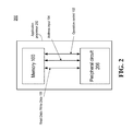
- FIG. 1 is a block diagram of an exemplary embodiment of a memory.
- FIG. 2 is a block diagram of an exemplary embodiment of an application processor incorporating the memory of FIG. 1 .
- FIG. 3 is a schematic diagram of an exemplary embodiment of a memory cell for an SRAM.
- FIG. 4 is a functional block diagram of an exemplary embodiment of an SRAM.
- FIG. 5 is a circuit diagram of an exemplary embodiment of a write driver outputting and adjusting a voltage level of a wordline.
- FIG. 6 is a diagram of wordline voltage levels for different cases of the parameter of the transistor of the memory cell.
- FIG. 7 is a diagram of a perspective view of a physical implementation of an exemplary transistor.
- FIG. 8 is the flowchart of operations of the SRAM of FIG. 4 .
- Various memories and methods for reading from and/or writing to memory presented throughout this disclosure may be incorporated within various apparatuses.
- various aspects of memories disclosed herein may be implemented as or in a stand-alone memory. Such aspects may also be included in any integrated circuit (IC) or system, or any portion of an integrated circuit or system (e.g., modules, components, circuits, or the like residing in an integrated circuit or part of an integrated circuit), or any intermediate product where an integrated circuit or system is combined with other integrated circuits or systems (e.g., a video card, a motherboard, etc.) or any end product (e.g., mobile phone, personal digital assistant (PDA), desktop computer, laptop computer, palm-sized computer, tablet computer, work station, game console, media player, computer based simulators, wireless communication attachments for laptops, or the like).
- PDA personal digital assistant
- connection means any connection or coupling, either direct or indirect, between two or more elements, and can encompass the presence of one or more intermediate elements between two elements that are “connected” or “coupled” together.
- the coupling or connection between the elements can be physical, logical, or a combination thereof.
- two elements can be considered to be “connected” or “coupled” together by the use of one or more wires, cables and/or printed electrical connections, as well as by the use of electromagnetic energy, such as electromagnetic energy having wavelengths in the radio frequency region, the microwave region and the optical (both visible and invisible) region, as several non-limiting and non-exhaustive examples.
- any reference to an element herein using a designation such as “first,” “second,” and so forth does not generally limit the quantity or order of those elements. Rather, these designations are used herein as a convenient method of distinguishing between two or more elements or instances of an element. Thus, a reference to first and second elements does not mean that only two elements can be employed, or that the first element must precede the second element.
- SRAM static random access memory
- IC integrated circuit
- embedded SRAM is an application processor for wireless communication applications.
- FIG. 1 is a block diagram of an exemplary embodiment of a memory 100 .
- the memory 100 provides a medium for peripheral circuits to write and read data (e.g., program instructions and data operated by the instruction).
- data will be understood to include program instructions, data, and any other information that may be stored in the memory 100 .
- the memory 100 includes an input for an operation control 102 for controlling an operation of the memory 100 .
- the memory 100 may operate in read, write, or various test modes.
- the memory 100 also includes inputs for the address (e.g., via the address input 104 ) and for write data (e.g., via the read data/write data 106 ) to be written to the memory 100 at the specified address.
- the memory further includes an output for read data (e.g., via the read data/write data 106 ) read from the memory 100 at the specified address.
- a peripheral circuit sets the operation control 102 to the write mode and sends to the memory 100 the address along with the write data to be written to the memory 100 at that address.
- the peripheral circuit sets the read/write enable control to the read mode and sends the address to the memory 100 .
- the memory 100 sends read data at that address to the peripheral circuit.
- FIG. 2 is a block diagram of an exemplary embodiment of an application processor incorporating the memory of FIG. 1 .
- the application processor 202 is provided as an example of an IC substrate having the memory 100 of FIG. 1 incorporated therein. As is known by a person of ordinary skill in the art, applications of the memory 100 are not limited thereto.
- the application processor 202 may be incorporated in the IC substrate upon which the memory 100 and various processor cores are incorporated.
- a processor core may be a collection of circuits and may include an instruction execution unit.
- One of the processor cores may operate as or include the peripheral circuit 206 .
- the peripheral circuit 206 may be construed broadly to include any suitable circuit that is peripheral to the memory 100 and capable of accessing the memory 100 . As described with FIG.
- the peripheral circuit 206 may instruct the memory 100 to execute a read or write operation via the operation control 102 and the address input 104 .
- the peripheral circuit 206 may further receive the read data from the memory 100 or provide the write data to the memory 100 via the read data/write data 106 .
- the memory 100 may be any suitable storage medium, such as, by way of example, an SRAM. However, as those skilled in the art will readily appreciate, the memory 100 is not necessarily limited to SRAM.
- An SRAM includes an array of storage elements know as “cells,” “memory cells,” or “bitcells.” Each memory cell is configured to store one bit of data (e.g., logic 1 or logic 0).
- FIG. 3 is a circuit diagram of an exemplary embodiment of a memory cell for an SRAM.
- the memory cell 300 is implemented with a six-transistor (6T) configuration. However, as those skilled in the art will readily appreciate, the cell may be implemented with a four-transistor (4T) or any other suitable transistor configuration.
- the memory cell 300 is shown with two inverters 302 , 304 .
- the first inverter 302 includes a p-channel transistor 306 and an n-channel transistor 308 .
- the second inverter 304 includes a p-channel transistor 310 and an n-channel transistor 312 .
- the inverters 302 and 304 are powered by VDD and have a return VSS (e.g., ground).
- the first and second inverters 302 , 304 are interconnected to form a cross-coupled latch.
- a first n-channel access transistor 314 couples the output node 316 from the first inverter 302 to a bitline BL
- a second n-channel access transistor 318 couples the output node 320 from the second inverter 304 to a bitline BLB (the value of which is the opposite or inverse of the bitline BL).
- the gates of the access transistors 314 , 318 are coupled to a wordline WL.
- a read operation may be initiated by precharging or charging the bitlines BL and BLB to a predetermined level, which is determined so as not to disturb the stored data in the memory cell 300 . (The charge circuit is not shown for clarity).
- the wordline WL then is asserted, connecting the cross-coupled inverters 302 , 304 to the bitlines BL and BLB via the access transistors 314 and 318 , respectively.
- the memory cell 300 may store the logic 1 by storing a low level (e.g., ground) at the output node 316 and a high level (e.g., VDD) at the output node 320 . These states are maintained by the cross-coupled inverters 302 , 304 .
- the inverter 302 Upon asserting the wordline WL, the inverter 302 discharges the bitline BL through the access transistor 314 and the output node 316 .
- the bitline BLB is maintained at the high level by the inverter 304 through the access transistor 318 and the output node 320 .
- a voltage difference on the bitline pair BL and BLB is thus established by the pulling-down of the bitline BL.
- the bitlines BL and BLB are fed to a sense amplifier (SA), which senses the data (e.g., voltage difference) carried thereon and outputs a logic level (e.g., logic 1) as the read data to the peripheral circuit 206 .
- SA sense amplifier
- a write operation is used as an example (but the score of the disclosure is certainly no limited thereto). According, the SA is not shown for clarity.
- a write operation may be initiated by setting the bitlines BL and BLB to the value to be written to the memory cell 300 and asserting the wordline WL. That is, the write data are driven onto the bitlines BL and BLB.
- the wordline WL may be asserted before or after the value to be written (e.g., write data) is provided to the bitlines BL and BLB.
- a logic 1 may be written to the memory cell 300 by setting the bitline BL to a logic level 0 and the bitline BLB to a logic 1.
- the logic level 0 at the bitline BL is applied to the input of the second inverter 304 through the access transistor 314 , which in turn forces the output node 320 of the second inverter 304 to VDD.
- the output node 320 of the second inverter 304 is applied to the input of the first inverter 302 , which in turn forces the output node 316 of the first inverter 302 to VSS.
- a logic level 0 may be written to the memory cell 300 by inverting the values of the bitlines BL and BLB.
- the write driver is designed to be stronger than the pull-up transistors ( 306 and 310 ) in the memory cell 300 so that the write data can override the previous state of the cross-coupled inverters 302 , 304 .
- the wordline is de-asserted, thereby causing the access transistors 314 and 318 to disconnect the bitlines BL and BLB from the two inverters 302 , 304 .
- the cross-coupling between the two inverters 302 , 304 maintains the state of the inverter outputs as long as power is applied to the memory cell 300 .
- FIG. 4 is a functional block diagram of an exemplary embodiment of an SRAM.
- SRAM static random access memory
- FIG. 4 is a functional block diagram of an exemplary embodiment of an SRAM.
- Various aspects of an SRAM will now be presented in the context of a write operation. Accordingly, for clarity of presentation, only the connections for the write operation are shown. Those skilled in the art will readily appreciate that additional connections are required to support the read operation.
- the SRAM 400 is configured to implement an improved scheme to adjust the voltage level on the wordline to, for example, improve SNM.
- the SRAM 400 includes a core 402 with supporting circuitry to decode addresses and perform read and write operations.
- the core 402 includes memory cells 300 arranged to share connections in horizontal rows and vertical columns. Specifically, each horizontal row of memory cells 300 shares a wordline WL and each vertical column of memory cells 300 shares a pair of bitlines BL and BLB.
- the size of the core 402 (i.e., the number of cells) may vary depending on a variety of factors including the specific application, the speed requirements, the layout and testing requirements, and the overall design constraints imposed on the system. Typically, the core 402 will contain thousands or millions of memory cells.
- the core 402 is made up of (2 n ⁇ 2 m (x)) memory cells 300 arranged in T horizontal rows and 2 m (x) vertical columns, where 2 m is the number of words per row and x is the number of bits per word.
- a peripheral device may randomly access any word (i.e., x cells) in the core 402 using an address that is (n+m) bits wide.
- the SRAM 400 outputs x-bits read data for a read operation, and writes x-bits write data into the core 402 for a write operation.
- n-bits of the address are provided to the input of a row decoder 404 and m-bits of the address are provided to the input of a column decoder 406 .
- the row decoder 404 converts the n-bit address into 2 n wordline outputs.
- a different wordline WL is asserted by the row decoder 404 for each different n-bit row address.
- each of the 2 m (x) memory cells 300 in the horizontal row with the asserted wordline WL is connected to one pair of the 2 m (x) bitlines (BL and BLB) through its access transistors as described above in connection with FIG. 3 .
- the row decoder 404 may include wordline drivers 405 (1:2 n ) to output a voltage level onto each of the WL wordlines. Additional features relating to the wordline drivers 405 (1:2 n ) are provided with FIG. 5 .
- the write data is driven, through the x multiplexers 408 , onto the selected pairs of bitlines (BL and BLB) and written to the memory cells with the asserted wordline WL, as described with FIG. 3 .
- the column decoder 406 provides 2 m outputs (WM 1 -WM 2 m ) with a different one of the outputs asserted for each different combination of address inputs.
- the outputs are provided to x multiplexers 408 .
- Each multiplexer is 2 m :1 multiplexer which switches one of x inputs from the write driver 410 between 2 m bitline pairs based on the outputs from the column decoder 406 .
- a core that stores four 128-bit words per row requires 128 4:1 multiplexers (e.g., x is four in this example).
- Each multiplexer input is coupled to one of 128 outputs from the write driver 410 .
- each multiplexer couples its input from the write driver 410 to one of four bitline pairs.
- the four bitline pairs are coupled to four memory cells, each storing a corresponding bit for a different word in a row.
- the first of the four memory cells may store the least significant bit (LSB) of the first word
- the second of the four memory cells may store the LSB of the second word
- the third of the four memory cells may store the LSB of the third word
- the fourth of the four memory cells may store the LSB of the fourth word.
- the write driver 410 drives the write data received from the peripheral device (not shown) onto x pairs of bitlines BL and BLB with each of the x multiplexers providing one pair of bitlines BL and BLB.
- FIG. 5 is a circuit diagram of an exemplary embodiment of a write driver outputting and adjusting a voltage level of a wordline.
- One scheme to improve the SNM (and therefore further lowers the minimum operating voltage of the memory) is to adjust the wordline voltage.
- the wordline voltage e.g., a voltage level when the wordline WL is asserted to access the memory cell 300
- the asserted wordline is coupled to 2 m (x) memory cells 300 , among which x memory cells 300 may be selected for write.
- the unselected memory cells 300 may be put in pseudo-read condition.
- the bitline pair BL and BL_B for the unselected memory cell 300 may be precharged to a voltage level, such as VDD, that does not disturb the stored data upon an assertion of the wordline WL.
- the scheme is more susceptible to noise under certain conditions.
- the unselected memory cell 300 may store a logic 0 at the node 316 .
- the bitline pair BL and BL_B is charged to VDD for the unselected memory cell 300 .
- the access transistor 314 may be stronger than normal, and noise may cause the VDD level on the bitline BL to overwrite, via the strong access transistor 314 , the stored logic 0 at the node 316 .
- the SRAM 400 is more susceptible to noise for a case of faster n-type transistor than a case of slower n-type transistor
- adjusting or lowering the wordline voltage may improve the SNM.
- the effect of faster n-type transistor may be mitigated.
- the VDD on the bitline BL would not be able to falsely overwrite the stored logic 0 at the node 316 with the lowered wordline WL, as the drive of the access transistor 314 would be diminished by the lower wordline WL.
- other issues may arise. For example, under the condition of slower n-type transistor (and faster p-type transistor), overwriting the stored data in the selected memory cell 300 may be more difficult. Thus, adjusting or lowering the wordline may impact the write performance.
- the circuit diagram 500 depicts an exemplary embodiment of a write driver 405 that improves the SNM for some conditions (e.g., faster n-type transistor) without degrading the write capability of memory cell for other conditions (e.g., slower n-type transistor) by the same level.
- the wordline driver 405 includes a buffer 502 powered by the voltage supply VDD and a voltage adjustment circuit 405 _ 1 .
- the buffer 502 may include an inverter.
- the buffer 502 in response to the decoded n-bit address, outputs the wordline voltage at VDD onto the wordline WL.
- the voltage adjustment circuit 405 _ 1 is configured to adjust the wordline voltage by an adjustment amount V ADJ to compensate for a parameter of a (reference) transistor in the memory cell 300 .
- the adjustment amount V ADJ may vary in accordance or in response to the parameter of the (reference) transistor in the memory cell 300 .
- the (reference) transistor may be the access transistor 314 or 318 .
- the parameter may include the speed of the (reference) transistor. For example, a case of faster speed may include the (reference) transistor having a higher transconductance and/or lower threshold voltage V TH , compared to a case of lower speed.
- the parameter of the (reference) transistor may additionally take temperature into account.
- the voltage adjustment circuit 405 _ 1 includes an n-type pull-down transistor 514 coupled to the wordline WL.
- the pull-down transistor 514 is configured to adjust or pull down the wordline voltage on the wordline WL.
- the pull-down transistor 514 is configured to pull down the voltage level on the wordline WL more in a case of faster sleep of n-type transistor than in a case of slower speed of the (reference) transistor (and pull down the wordline voltage less in a case of slower n-type transistor).
- the voltage adjustment circuit 405 _ 1 further includes an n-type passgate transistor 512 to bias the pull-down transistor 514 .
- the passgate transistor 512 couples the gate of the pull-down transistor 514 and the wordline WL to control the adjusting or pulling down of the wordline voltage.
- a feedback of the wordline 550 feeds back the wordline voltage level via the passgate transistor 512 and the pull-down transistor 514 .
- the wordline WL is electrically connected to the gate of the pull-down transistor.
- the adjustment amount V ADJ is thus based on a present voltage level of the wordline WL.
- the wordline driver is configured to adjust a voltage level of the wordline WL based on a feedback of the wordline.
- the adjustment amount V ADJ varies according to the parameter of the (reference) transistor of the memory cell 300 .
- voltage adjustment circuit 405 _ 1 is configured such that the adjustment amount V ADJ is greater in a case of a faster speed than a case of slower speed of the (reference) transistor. In such fashion, the impact of adjusting or lowering the wordline voltage is reduced in the case of slower speed of the (reference) transistor.
- the (reference) transistor of the memory cell 300 may be the n-type transistor, such as the access transistor 314 or 318 , of the memory cell 300 .
- a higher adjustment amount V ADJ may be needed to improve the SNM (e.g., for write).
- the unselected memory cells 300 are less susceptible to noise (which otherwise might cause disturbance of the stored data due to the faster speed of the n-type access transistor 314 or 318 ).
- a lower adjustment amount V ADJ may be applied.
- the write data on the bitline pairs BL and BL_B overcome the data stored in the memory cells 300 .
- V ADJ By reducing the adjustment amount V ADJ in the case of slower speed of n-type transistor, such write process is not impeded. Additional details regarding the operation of the voltage adjustment circuit 405 _ 1 are presented with FIG. 6 .
- the voltage adjustment circuit 405 _ 1 may further be configured to be disabled (e.g., does not adjust or pull down the wordline voltage).
- a control circuit 520 powered by the voltage supply VDD asserts the WL_ADJ signal to enable voltage adjustment circuit 405 _ 1 .
- the asserted WL_ADJ signal may thus be at VDD level and is provided to the gate of the passgate transistor 512 to turn on the passgate transistor 512 .
- the inverter 542 receives the WL_ADJ signal and outputs the WL_ADJ_B signal, which is of the opposite polarity of the WL_ADJ signal.
- the n-type transistor 516 couples the node N 1 , which is connected to the gate of the pull-down transistor 514 , and ground VSS.
- the n-type transistor 516 When the WL_ADJ signal is asserted, the n-type transistor 516 is turned off and does not affect the operation of the voltage adjustment circuit 405 _ 1 .
- the passgate transistor 512 When the WL_ADJ signal is de-asserted to disable the voltage adjustment circuit 405 _ 1 , the passgate transistor 512 to turn off by the WL_ADJ signal, and the transistor 516 is turned on by the WL_ADJ_B signal.
- the turned-on transistor 516 pulls the node N 1 to ground to disable the pull-down transistor 514 .
- FIG. 6 is a diagram of wordline voltage levels for different cases of the parameter of the transistor of the memory cell.
- the parameter compensated may include the threshold voltage V TH of the n-type transistor of the memory cell 300 .
- the n-type transistor of the memory cell 300 is faster (than that of case 2 ), and therefore, the V TH of n-type transistor may be lower (than that of case 2 ).
- the n-type transistor of the memory cell 300 is slower (than that of case 1 ), and therefore, the V TH of n-type transistor may be higher (than that of case 1 ).
- the wordline voltage When the voltage adjustment circuit 405 _ 1 is disabled, the wordline voltage would be unadjusted at VDD.
- the passgate transistor 512 couples the wordline WL to the node N 1 and therefore, to the gate of the pull-down transistor 514 .
- the voltage on the node N 1 would be the voltage of the WL_ADJ signal (i.e., VDD) subtracted by the V TH of the passgate transistor 512 .
- the voltage on the node N 1 turns on the pull-down transistor 514 to pull down the voltage on the wordline WL by the adjustment amount V ADJ .
- the V TH of the passgate transistor 512 is lower in case 1 (faster n-type transistor) than in case 2 (slower n-type transistor). Accordingly, the node N 1 voltage is higher in case 1 than in case 2 . As a result, the pull-down transistor 514 is turned on stronger in case 1 than in case 2 , and the wordline voltage is pull-down more (e.g., V ADJ is higher) in case 1 than in case 2 . The difference in the pulling-down of the wordline voltages in case 1 and case 2 is further expanded because of the lower V TH of the pull-down transistor 514 (which allows to the pull-down transistor 514 to turn on even stronger in case 1 than in case 2 ).
- FIG. 7 is a diagram of a perspective view of a physical implementation of an exemplary transistor.
- the SRAM 400 may be implemented in finFET technology.
- the transistor is fabricated in a vertical direction.
- Transistor 710 illustrates a transistor of a single fin in finFET technology.
- Transistor 720 illustrates a transistor of multiple fins.
- a fin may be a 3-D source, drain, and gate structure and is disposed on the field oxide (as opposed to being planar with field oxide).
- the fin_ 1 of the transistor 710 may extend in a first direction.
- a gate oxide layer is disposed on the gate region of the fin. The gate of the transistor extends over the fin in the second direction.
- the transistor 710 has a gate length L, and a source/drain width of W FIN and a source/drain height of H FIN .
- the transistor 720 is substantially the same as transistor 710 , but with fins fin_ 1 and fin_ 2 and having a common gate over the fins.
- the drive strength of the transistor 720 would thus be almost twice the drive strength of the transistor 710 .
- the size of a transistor may be determined by a number of fins of the transistor.
- the memory cell 300 is implemented in finFET technology.
- the p-type transistors 306 and 310 and the n-type transistors 308 and 312 configured as a latch to stored data are implemented in a same number of fin or fins (e.g., each is a transistor of one fin as illustrated by transistor 710 ).
- the p-type transistors 306 and 310 and the n-type transistors 308 and 312 latching the stored data are thus implemented as transistors of the same size.
- the access transistors 314 and 318 may also be implemented with the same number of fin or fins as the latching transistors (e.g., each is a transistor of one fin as illustrated by transistor 710 ).
- the access transistors 314 and 318 are thus transistors of the same size as the latching transistors.
- FIG. 8 is the flowchart of operations of the SRAM of FIG. 4 .
- the operations may be performed by, for example, circuits presented in FIGS. 4 and 5 .
- a wordline voltage is asserted to access a memory cell including a transistor.
- the wordline driver 405 asserts the wordline by outputting a voltage onto the wordline WL to access the memory cells 300 .
- the memory cell 300 may include p-type transistors 306 and 310 and n-type transistors 308 and 312 configured as a latch to store data.
- the access transistors 314 and 318 are coupled to the wordline WL to allow the bitline pair BL and BL_B to read or write the memory cell 300 .
- the wordline voltage is adjusted to compensate for a parameter of the transistor.
- the parameter of the transistor may be a speed of the n-type transistor (e.g., of the access transistors 314 and 318 ) of the memory cell 300 .
- the speed may include a transconductance and/or threshold voltage V TH of the n-type transistor.
- the voltage adjustment circuit 405 _ 1 adjusts or pulls down the voltage on the wordline WL based on the speed (e.g., transconductance and/or threshold voltage V TH ) of the n-type transistor.
- the wordline voltage is pulled down more in a case of faster n-type transistor.
- the wordline voltage is pulled-down less in a case of slower n-type transistor.
- the passgate transistor 512 couples the wordline WL to the node N 1 and therefore, to the gate of the pull-down transistor 514 .
- the voltage on the node N 1 would be the voltage of the WL_ADJ signal (i.e., VDD) subtracted by the V TH of the passgate transistor 512 .
- the voltage on the node N 1 turns on the pull-down transistor 514 to pull down the voltage on the wordline WL by the adjustment amount V ADJ .
- the V TH of the passgate transistor 512 is lower in case 1 (faster n-type transistor) than in case 2 (slower n-type transistor). Accordingly, the node N 1 voltage is higher in case 1 than in case 2 . As a result, the pull-down transistor 514 is turned on stronger in case 1 than in case 2 , and the wordline voltage is pull-down more (V ADJ is higher) in case 1 than in case 2 . The difference in the pulling-down of the wordline voltages in case 1 and case 2 is further expanded because of the lower V TH of the pull-down transistor 514 (which allows to the pull-down transistor 514 to turn on even stronger in case 1 than in case 2 .
- the wordline voltage is pulled down by a pull-down transistor.
- the pull-down transistor is biased by a passgate transistor.
- a gate of the pull-down transistor and the wordline voltage are coupled. Referring to FIG. 5 , the pull-down transistor 514 pulls down the voltage of the wordline WL.
- the passgate transistor 512 couples the voltage of the wordline WL to the gate of the pull-down transistor 514 (e.g., by way of the node N 1 ). The passgate transistor 512 thus biases the pull-down transistor 514 to adjust the wordline voltage.
Landscapes
- Engineering & Computer Science (AREA)
- Microelectronics & Electronic Packaging (AREA)
- Computer Hardware Design (AREA)
- Static Random-Access Memory (AREA)
- Semiconductor Memories (AREA)
Priority Applications (7)
| Application Number | Priority Date | Filing Date | Title |
|---|---|---|---|
| US15/085,942 US9928898B2 (en) | 2016-03-30 | 2016-03-30 | Wordline adjustment scheme |
| BR112018069830A BR112018069830A2 (pt) | 2016-03-30 | 2017-02-24 | esquema de ajuste de linha de palavra |
| KR1020187027956A KR102054920B1 (ko) | 2016-03-30 | 2017-02-24 | 워드라인 조정 방식 |
| EP17709316.8A EP3437098B1 (en) | 2016-03-30 | 2017-02-24 | Wordline adjustment scheme |
| JP2018550725A JP6545915B2 (ja) | 2016-03-30 | 2017-02-24 | ワード線調整スキーム |
| PCT/US2017/019488 WO2017172150A1 (en) | 2016-03-30 | 2017-02-24 | Wordline adjustment scheme |
| CN201780020747.5A CN108885890B (zh) | 2016-03-30 | 2017-02-24 | 字线调节方案 |
Applications Claiming Priority (1)
| Application Number | Priority Date | Filing Date | Title |
|---|---|---|---|
| US15/085,942 US9928898B2 (en) | 2016-03-30 | 2016-03-30 | Wordline adjustment scheme |
Publications (2)
| Publication Number | Publication Date |
|---|---|
| US20170287551A1 US20170287551A1 (en) | 2017-10-05 |
| US9928898B2 true US9928898B2 (en) | 2018-03-27 |
Family
ID=58231789
Family Applications (1)
| Application Number | Title | Priority Date | Filing Date |
|---|---|---|---|
| US15/085,942 Active US9928898B2 (en) | 2016-03-30 | 2016-03-30 | Wordline adjustment scheme |
Country Status (7)
| Country | Link |
|---|---|
| US (1) | US9928898B2 (zh) |
| EP (1) | EP3437098B1 (zh) |
| JP (1) | JP6545915B2 (zh) |
| KR (1) | KR102054920B1 (zh) |
| CN (1) | CN108885890B (zh) |
| BR (1) | BR112018069830A2 (zh) |
| WO (1) | WO2017172150A1 (zh) |
Cited By (2)
| Publication number | Priority date | Publication date | Assignee | Title |
|---|---|---|---|---|
| US20230008275A1 (en) * | 2021-07-09 | 2023-01-12 | Stmicroelectronics International N.V. | Adaptive word line underdrive control for an in-memory compute operation where simultaneous access is made to plural rows of a static random access memory (sram) |
| US11984151B2 (en) | 2021-07-09 | 2024-05-14 | Stmicroelectronics International N.V. | Adaptive bit line overdrive control for an in-memory compute operation where simultaneous access is made to plural rows of a static random access memory (SRAM) |
Families Citing this family (3)
| Publication number | Priority date | Publication date | Assignee | Title |
|---|---|---|---|---|
| US10811088B2 (en) * | 2019-03-12 | 2020-10-20 | Qualcomm Incorporated | Access assist with wordline adjustment with tracking cell |
| US20230260572A1 (en) * | 2022-02-15 | 2023-08-17 | Taiwan Semiconductor Manufacturing Company Ltd. | Electronic circuits, memory devices, and methods for operating an electronic circuit |
| US11842769B2 (en) * | 2022-04-14 | 2023-12-12 | Macronix International Co., Ltd. | Memory circuit with leakage current blocking mechanism and memory device having the memory circuit |
Citations (13)
| Publication number | Priority date | Publication date | Assignee | Title |
|---|---|---|---|---|
| US5410508A (en) * | 1993-05-14 | 1995-04-25 | Micron Semiconductor, Inc. | Pumped wordlines |
| US20060274569A1 (en) * | 2005-06-02 | 2006-12-07 | International Business Machines Corporation | Semiconductor device including back-gated transistors and method of fabricating the device |
| US20070030741A1 (en) | 2005-08-02 | 2007-02-08 | Renesas Technology Corp. | Semiconductor memory device |
| US20080037358A1 (en) * | 2006-08-10 | 2008-02-14 | Renesas Technology Corp. | Semiconductor memory device comprising a plurality of static memory cells |
| US20120033522A1 (en) | 2010-08-09 | 2012-02-09 | National Chiao Tung University | Variation-tolerant word-line under-drive scheme for random access memory |
| US20120075918A1 (en) | 2010-09-28 | 2012-03-29 | International Business Machines Corporation | SRAM Having Wordline Up-Level Voltage Adjustable to Assist Bitcell Stability and Design Structure for Same |
| US20120106237A1 (en) * | 2010-10-28 | 2012-05-03 | International Business Machines Corporation | Boost circuit for generating an adjustable boost voltage |
| US20140022835A1 (en) | 2012-07-23 | 2014-01-23 | Arm Limited | Controlling the voltage level on the word line to maintain performance and reduce access disturbs |
| US20140112065A1 (en) | 2012-10-24 | 2014-04-24 | Fujitsu Semiconductor Limited | Semiconductor memory device |
| US20150029799A1 (en) | 2013-07-24 | 2015-01-29 | Advanced Micro Devices, Inc. | Canary circuit with passgate transistor variation |
| US9001579B2 (en) | 2012-11-21 | 2015-04-07 | Samsung Electronics Co., Ltd. | Semiconductor memory device for and method of applying temperature-compensated word line voltage during read operation |
| CN104934068A (zh) | 2015-07-07 | 2015-09-23 | 合肥恒烁半导体有限公司 | 一种nand型闪存存储器读取操作时的字线电压生成电路 |
| US9202579B2 (en) | 2013-03-14 | 2015-12-01 | Sandisk Technologies Inc. | Compensation for temperature dependence of bit line resistance |
Family Cites Families (7)
| Publication number | Priority date | Publication date | Assignee | Title |
|---|---|---|---|---|
| JPS5819794A (ja) * | 1981-07-29 | 1983-02-04 | Fujitsu Ltd | 半導体メモリ |
| JP3239867B2 (ja) * | 1998-12-17 | 2001-12-17 | 日本電気株式会社 | 半導体装置 |
| JP4408610B2 (ja) * | 2002-08-09 | 2010-02-03 | 株式会社ルネサステクノロジ | スタティック型半導体記憶装置 |
| WO2005079447A2 (en) * | 2004-02-17 | 2005-09-01 | Agere Systems, Inc. | Switching power supply controller with built-in supply switching |
| US7760576B2 (en) * | 2007-11-08 | 2010-07-20 | Qualcomm Incorporated | Systems and methods for low power, high yield memory |
| JP5259270B2 (ja) * | 2008-06-27 | 2013-08-07 | ルネサスエレクトロニクス株式会社 | 半導体装置 |
| US9355710B2 (en) * | 2014-01-23 | 2016-05-31 | Nvidia Corporation | Hybrid approach to write assist for memory array |
-
2016
- 2016-03-30 US US15/085,942 patent/US9928898B2/en active Active
-
2017
- 2017-02-24 KR KR1020187027956A patent/KR102054920B1/ko active IP Right Grant
- 2017-02-24 CN CN201780020747.5A patent/CN108885890B/zh active Active
- 2017-02-24 BR BR112018069830A patent/BR112018069830A2/pt not_active IP Right Cessation
- 2017-02-24 EP EP17709316.8A patent/EP3437098B1/en active Active
- 2017-02-24 JP JP2018550725A patent/JP6545915B2/ja active Active
- 2017-02-24 WO PCT/US2017/019488 patent/WO2017172150A1/en active Application Filing
Patent Citations (13)
| Publication number | Priority date | Publication date | Assignee | Title |
|---|---|---|---|---|
| US5410508A (en) * | 1993-05-14 | 1995-04-25 | Micron Semiconductor, Inc. | Pumped wordlines |
| US20060274569A1 (en) * | 2005-06-02 | 2006-12-07 | International Business Machines Corporation | Semiconductor device including back-gated transistors and method of fabricating the device |
| US20070030741A1 (en) | 2005-08-02 | 2007-02-08 | Renesas Technology Corp. | Semiconductor memory device |
| US20080037358A1 (en) * | 2006-08-10 | 2008-02-14 | Renesas Technology Corp. | Semiconductor memory device comprising a plurality of static memory cells |
| US20120033522A1 (en) | 2010-08-09 | 2012-02-09 | National Chiao Tung University | Variation-tolerant word-line under-drive scheme for random access memory |
| US20120075918A1 (en) | 2010-09-28 | 2012-03-29 | International Business Machines Corporation | SRAM Having Wordline Up-Level Voltage Adjustable to Assist Bitcell Stability and Design Structure for Same |
| US20120106237A1 (en) * | 2010-10-28 | 2012-05-03 | International Business Machines Corporation | Boost circuit for generating an adjustable boost voltage |
| US20140022835A1 (en) | 2012-07-23 | 2014-01-23 | Arm Limited | Controlling the voltage level on the word line to maintain performance and reduce access disturbs |
| US20140112065A1 (en) | 2012-10-24 | 2014-04-24 | Fujitsu Semiconductor Limited | Semiconductor memory device |
| US9001579B2 (en) | 2012-11-21 | 2015-04-07 | Samsung Electronics Co., Ltd. | Semiconductor memory device for and method of applying temperature-compensated word line voltage during read operation |
| US9202579B2 (en) | 2013-03-14 | 2015-12-01 | Sandisk Technologies Inc. | Compensation for temperature dependence of bit line resistance |
| US20150029799A1 (en) | 2013-07-24 | 2015-01-29 | Advanced Micro Devices, Inc. | Canary circuit with passgate transistor variation |
| CN104934068A (zh) | 2015-07-07 | 2015-09-23 | 合肥恒烁半导体有限公司 | 一种nand型闪存存储器读取操作时的字线电压生成电路 |
Non-Patent Citations (2)
| Title |
|---|
| International Search Report and Written Opinion-PCT/US2017/019488-ISA/EPO-dated Jun. 13, 2017. |
| International Search Report and Written Opinion—PCT/US2017/019488—ISA/EPO—dated Jun. 13, 2017. |
Cited By (2)
| Publication number | Priority date | Publication date | Assignee | Title |
|---|---|---|---|---|
| US20230008275A1 (en) * | 2021-07-09 | 2023-01-12 | Stmicroelectronics International N.V. | Adaptive word line underdrive control for an in-memory compute operation where simultaneous access is made to plural rows of a static random access memory (sram) |
| US11984151B2 (en) | 2021-07-09 | 2024-05-14 | Stmicroelectronics International N.V. | Adaptive bit line overdrive control for an in-memory compute operation where simultaneous access is made to plural rows of a static random access memory (SRAM) |
Also Published As
| Publication number | Publication date |
|---|---|
| CN108885890A (zh) | 2018-11-23 |
| CN108885890B (zh) | 2020-01-03 |
| KR20180113615A (ko) | 2018-10-16 |
| JP6545915B2 (ja) | 2019-07-17 |
| JP2019510333A (ja) | 2019-04-11 |
| BR112018069830A2 (pt) | 2019-01-29 |
| EP3437098A1 (en) | 2019-02-06 |
| US20170287551A1 (en) | 2017-10-05 |
| EP3437098B1 (en) | 2019-07-24 |
| KR102054920B1 (ko) | 2019-12-11 |
| WO2017172150A1 (en) | 2017-10-05 |
Similar Documents
| Publication | Publication Date | Title |
|---|---|---|
| US9401201B1 (en) | Write driver for memory | |
| US9646681B1 (en) | Memory cell with improved write margin | |
| EP3437098B1 (en) | Wordline adjustment scheme | |
| JP6308831B2 (ja) | 半導体記憶装置 | |
| US7403426B2 (en) | Memory with dynamically adjustable supply | |
| US9875788B2 (en) | Low-power 5T SRAM with improved stability and reduced bitcell size | |
| US20150310901A1 (en) | Memory with a sleep mode | |
| US10811088B2 (en) | Access assist with wordline adjustment with tracking cell | |
| US10325648B2 (en) | Write driver scheme for bit-writable memories | |
| US20160093365A1 (en) | Seven-transistor static random-access memory bitcell with reduced read disturbance | |
| US20150228314A1 (en) | Level shifters for systems with multiple voltage domains | |
| WO2012081159A1 (ja) | 半導体記憶装置 | |
| US10140044B2 (en) | Efficient memory bank design | |
| EP3411877B1 (en) | Shared sense amplifier | |
| US10140224B2 (en) | Noise immune data path scheme for multi-bank memory architecture | |
| US20150279452A1 (en) | Memory having a pull-up circuit with inputs of multiple voltage domains | |
| US11488658B2 (en) | Write assist scheme with bitline | |
| US9978444B2 (en) | Sense amplifier enabling scheme | |
| JP2008176907A (ja) | 半導体記憶装置 | |
| JP2018092698A (ja) | 半導体記憶装置 | |
| US9627041B1 (en) | Memory with a voltage-adjustment circuit to adjust the operating voltage of memory cells for BTI effect screening |
Legal Events
| Date | Code | Title | Description |
|---|---|---|---|
| AS | Assignment |
Owner name: QUALCOMM INCORPORATED, CALIFORNIA Free format text: ASSIGNMENT OF ASSIGNORS INTEREST;ASSIGNORS:SAHU, RAHUL;GUPTA, SHARAD KUMAR;REEL/FRAME:039013/0221 Effective date: 20160624 |
|
| STCF | Information on status: patent grant |
Free format text: PATENTED CASE |
|
| MAFP | Maintenance fee payment |
Free format text: PAYMENT OF MAINTENANCE FEE, 4TH YEAR, LARGE ENTITY (ORIGINAL EVENT CODE: M1551); ENTITY STATUS OF PATENT OWNER: LARGE ENTITY Year of fee payment: 4 |