US9697786B2 - Display device - Google Patents
Display device Download PDFInfo
- Publication number
- US9697786B2 US9697786B2 US14/310,581 US201414310581A US9697786B2 US 9697786 B2 US9697786 B2 US 9697786B2 US 201414310581 A US201414310581 A US 201414310581A US 9697786 B2 US9697786 B2 US 9697786B2
- Authority
- US
- United States
- Prior art keywords
- vertical
- insulating film
- scan line
- sub
- line
- Prior art date
- Legal status (The legal status is an assumption and is not a legal conclusion. Google has not performed a legal analysis and makes no representation as to the accuracy of the status listed.)
- Active, expires
Links
Images


Classifications
-
- G—PHYSICS
- G09—EDUCATION; CRYPTOGRAPHY; DISPLAY; ADVERTISING; SEALS
- G09F—DISPLAYING; ADVERTISING; SIGNS; LABELS OR NAME-PLATES; SEALS
- G09F9/00—Indicating arrangements for variable information in which the information is built-up on a support by selection or combination of individual elements
- G09F9/30—Indicating arrangements for variable information in which the information is built-up on a support by selection or combination of individual elements in which the desired character or characters are formed by combining individual elements
- G09F9/35—Indicating arrangements for variable information in which the information is built-up on a support by selection or combination of individual elements in which the desired character or characters are formed by combining individual elements being liquid crystals
-
- G—PHYSICS
- G09—EDUCATION; CRYPTOGRAPHY; DISPLAY; ADVERTISING; SEALS
- G09G—ARRANGEMENTS OR CIRCUITS FOR CONTROL OF INDICATING DEVICES USING STATIC MEANS TO PRESENT VARIABLE INFORMATION
- G09G3/00—Control arrangements or circuits, of interest only in connection with visual indicators other than cathode-ray tubes
- G09G3/20—Control arrangements or circuits, of interest only in connection with visual indicators other than cathode-ray tubes for presentation of an assembly of a number of characters, e.g. a page, by composing the assembly by combination of individual elements arranged in a matrix no fixed position being assigned to or needed to be assigned to the individual characters or partial characters
- G09G3/34—Control arrangements or circuits, of interest only in connection with visual indicators other than cathode-ray tubes for presentation of an assembly of a number of characters, e.g. a page, by composing the assembly by combination of individual elements arranged in a matrix no fixed position being assigned to or needed to be assigned to the individual characters or partial characters by control of light from an independent source
- G09G3/36—Control arrangements or circuits, of interest only in connection with visual indicators other than cathode-ray tubes for presentation of an assembly of a number of characters, e.g. a page, by composing the assembly by combination of individual elements arranged in a matrix no fixed position being assigned to or needed to be assigned to the individual characters or partial characters by control of light from an independent source using liquid crystals
- G09G3/3611—Control of matrices with row and column drivers
- G09G3/3648—Control of matrices with row and column drivers using an active matrix
-
- G—PHYSICS
- G02—OPTICS
- G02F—OPTICAL DEVICES OR ARRANGEMENTS FOR THE CONTROL OF LIGHT BY MODIFICATION OF THE OPTICAL PROPERTIES OF THE MEDIA OF THE ELEMENTS INVOLVED THEREIN; NON-LINEAR OPTICS; FREQUENCY-CHANGING OF LIGHT; OPTICAL LOGIC ELEMENTS; OPTICAL ANALOGUE/DIGITAL CONVERTERS
- G02F1/00—Devices or arrangements for the control of the intensity, colour, phase, polarisation or direction of light arriving from an independent light source, e.g. switching, gating or modulating; Non-linear optics
- G02F1/01—Devices or arrangements for the control of the intensity, colour, phase, polarisation or direction of light arriving from an independent light source, e.g. switching, gating or modulating; Non-linear optics for the control of the intensity, phase, polarisation or colour
- G02F1/13—Devices or arrangements for the control of the intensity, colour, phase, polarisation or direction of light arriving from an independent light source, e.g. switching, gating or modulating; Non-linear optics for the control of the intensity, phase, polarisation or colour based on liquid crystals, e.g. single liquid crystal display cells
- G02F1/133—Constructional arrangements; Operation of liquid crystal cells; Circuit arrangements
- G02F1/136—Liquid crystal cells structurally associated with a semi-conducting layer or substrate, e.g. cells forming part of an integrated circuit
- G02F1/1362—Active matrix addressed cells
- G02F1/136286—Wiring, e.g. gate line, drain line
-
- G—PHYSICS
- G02—OPTICS
- G02F—OPTICAL DEVICES OR ARRANGEMENTS FOR THE CONTROL OF LIGHT BY MODIFICATION OF THE OPTICAL PROPERTIES OF THE MEDIA OF THE ELEMENTS INVOLVED THEREIN; NON-LINEAR OPTICS; FREQUENCY-CHANGING OF LIGHT; OPTICAL LOGIC ELEMENTS; OPTICAL ANALOGUE/DIGITAL CONVERTERS
- G02F1/00—Devices or arrangements for the control of the intensity, colour, phase, polarisation or direction of light arriving from an independent light source, e.g. switching, gating or modulating; Non-linear optics
- G02F1/01—Devices or arrangements for the control of the intensity, colour, phase, polarisation or direction of light arriving from an independent light source, e.g. switching, gating or modulating; Non-linear optics for the control of the intensity, phase, polarisation or colour
- G02F1/13—Devices or arrangements for the control of the intensity, colour, phase, polarisation or direction of light arriving from an independent light source, e.g. switching, gating or modulating; Non-linear optics for the control of the intensity, phase, polarisation or colour based on liquid crystals, e.g. single liquid crystal display cells
- G02F1/133—Constructional arrangements; Operation of liquid crystal cells; Circuit arrangements
- G02F1/1333—Constructional arrangements; Manufacturing methods
- G02F1/1345—Conductors connecting electrodes to cell terminals
- G02F1/13456—Cell terminals located on one side of the display only
-
- G—PHYSICS
- G02—OPTICS
- G02F—OPTICAL DEVICES OR ARRANGEMENTS FOR THE CONTROL OF LIGHT BY MODIFICATION OF THE OPTICAL PROPERTIES OF THE MEDIA OF THE ELEMENTS INVOLVED THEREIN; NON-LINEAR OPTICS; FREQUENCY-CHANGING OF LIGHT; OPTICAL LOGIC ELEMENTS; OPTICAL ANALOGUE/DIGITAL CONVERTERS
- G02F1/00—Devices or arrangements for the control of the intensity, colour, phase, polarisation or direction of light arriving from an independent light source, e.g. switching, gating or modulating; Non-linear optics
- G02F1/01—Devices or arrangements for the control of the intensity, colour, phase, polarisation or direction of light arriving from an independent light source, e.g. switching, gating or modulating; Non-linear optics for the control of the intensity, phase, polarisation or colour
- G02F1/13—Devices or arrangements for the control of the intensity, colour, phase, polarisation or direction of light arriving from an independent light source, e.g. switching, gating or modulating; Non-linear optics for the control of the intensity, phase, polarisation or colour based on liquid crystals, e.g. single liquid crystal display cells
- G02F1/133—Constructional arrangements; Operation of liquid crystal cells; Circuit arrangements
- G02F1/136—Liquid crystal cells structurally associated with a semi-conducting layer or substrate, e.g. cells forming part of an integrated circuit
- G02F1/1362—Active matrix addressed cells
- G02F1/136218—Shield electrodes
-
- G02F2001/13456—
-
- G02F2001/136218—
-
- G—PHYSICS
- G09—EDUCATION; CRYPTOGRAPHY; DISPLAY; ADVERTISING; SEALS
- G09G—ARRANGEMENTS OR CIRCUITS FOR CONTROL OF INDICATING DEVICES USING STATIC MEANS TO PRESENT VARIABLE INFORMATION
- G09G2300/00—Aspects of the constitution of display devices
- G09G2300/04—Structural and physical details of display devices
- G09G2300/0421—Structural details of the set of electrodes
- G09G2300/0426—Layout of electrodes and connections
-
- G—PHYSICS
- G09—EDUCATION; CRYPTOGRAPHY; DISPLAY; ADVERTISING; SEALS
- G09G—ARRANGEMENTS OR CIRCUITS FOR CONTROL OF INDICATING DEVICES USING STATIC MEANS TO PRESENT VARIABLE INFORMATION
- G09G2310/00—Command of the display device
- G09G2310/02—Addressing, scanning or driving the display screen or processing steps related thereto
- G09G2310/0264—Details of driving circuits
- G09G2310/0281—Arrangement of scan or data electrode driver circuits at the periphery of a panel not inherent to a split matrix structure
-
- G—PHYSICS
- G09—EDUCATION; CRYPTOGRAPHY; DISPLAY; ADVERTISING; SEALS
- G09G—ARRANGEMENTS OR CIRCUITS FOR CONTROL OF INDICATING DEVICES USING STATIC MEANS TO PRESENT VARIABLE INFORMATION
- G09G2320/00—Control of display operating conditions
- G09G2320/02—Improving the quality of display appearance
- G09G2320/0223—Compensation for problems related to R-C delay and attenuation in electrodes of matrix panels, e.g. in gate electrodes or on-substrate video signal electrodes
Definitions
- the present disclosure relates to a display device.
- FPD flat panel displays
- LCD liquid crystal displays
- OLED organic light emitting diode
- PDP plasma display panels
- the liquid crystal display that may achieve a high resolution and that may be manufactured as a large-sized display as well as a small-sized display has been widely used.
- the liquid crystal display displays an image by adjusting an arrangement direction of a liquid crystal layer in an electric field applied to a pixel electrode and a common electrode included in a liquid crystal panel so as to emit light irradiated from a backlight unit.
- the liquid crystal display is manufactured by being divided into various driving methods depending on a structure of the pixel electrode and the common electrode included in the liquid crystal panel.
- An aspect of the present invention provides a display device including: a display panel having vertical lines and horizontal lines formed thereon; sub-pixels formed on the display panel and including a pixel electrode and a common electrode; and a driver supplying a data signal and a scan signal to the sub-pixels through the vertical lines and horizontal lines, the vertical lines include a vertical data line to which the data signal is supplied and a vertical scan line to which the scan signal is supplied, the horizontal lines are connected to the vertical scan line and include a horizontal scan line transferring the scan signal in a horizontal direction, and the display panel include a shield electrode for shielding a signal interference between the pixel electrode and the vertical scan line.
- FIG. 1 is a schematic block configuration view of a display device according to a first embodiment of the present invention
- FIG. 2 is a configuration view of a display device that a portion of the block illustrated in FIG. 1 is modularized;
- FIG. 3 is enlarged view of a chip on film (COF) illustrated in FIG. 2 ;
- FIG. 4 is a first exemplified view of a pixel array
- FIG. 5 is a second exemplified view of a pixel array
- FIG. 6 is a view illustrating a connection relationship between vertical scanning lines and horizontal scanning lines
- FIG. 7 is a plan view illustrating a sub-pixel according to a first embodiment of the present invention.
- FIG. 8 is a cross-sectional view of a region taken along line A 1 -A 2 illustrated in FIG. 7 ;
- FIG. 9 is a cross-sectional view of a region taken along line B 1 -B 2 illustrated in FIG. 7 ;
- FIGS. 10 a and 10 b are cross-sectional views for comparing explaining a comparative example and a first embodiment
- FIG. 11 is a cross-sectional view of a region taken along line B 1 -B 2 illustrated in FIG. 7 according to a second embodiment of the present invention.
- FIG. 12 is a cross-sectional view of a region taken along line B 1 -B 2 illustrated in FIG. 7 according to a third embodiment of the present invention.
- FIG. 13 is a cross-sectional view of a region taken along line B 1 -B 2 illustrated in FIG. 7 according to a fourth embodiment of the present invention.
- FIG. 14 is a cross-sectional view of a region taken along line B 1 -B 2 illustrated in FIG. 7 according to a fifth embodiment of the present invention.
- FIG. 1 is a schematic block configuration view of a display device according to a first embodiment of the present invention
- FIG. 2 is a configuration view of a display device that a portion of the block illustrated in FIG. 1 is modularized
- FIG. 3 is enlarged view of a chip on film (COF) illustrated in FIG. 2 .
- COF chip on film
- the display device includes a display panel PNL, a driver DIC 10 , a timing controller TCON 12 , a host system SYSTEM 14 , and the like.
- the host system SYSTEM 14 converts a digital video data of an input image into a format suitable for the display panel PNL.
- the host system SYSTEM 14 supplies timing signals (Vsync, Hsync, DE, MCLK, and the like) together with the digital video data of the input image to the timing controller TCON 12 .
- the timing controller TCON 12 supplies the digital video data of the input image supplied from the host system 14 to the driver 10 .
- the timing controller 12 receives the timing signals such as a vertical synchronization signal (Vsync), a horizontal synchronization signal (Hsync), a data enable signal (DE), a main clock (MCLK), and the like from the host system 14 .
- the timing controller 12 generates a source timing control signal and a gate timing control signal to control the driver 10 using the timing signals such as the Vsync, Hsync, DE, and CLK.
- the display panel PNL may be implemented by depositing a thin film, such as the liquid crystal display panel, the organic light emitting display panel, an electrophoretic display panel, an the like
- a thin film such as the liquid crystal display panel, the organic light emitting display panel, an electrophoretic display panel, an the like
- the liquid crystal display panel PNL as an example of the display panel PNL will be described below.
- the liquid crystal display panel PNL may be implemented in all known liquid crystal modes such as a twisted nematic (TN) mode, a vertical alignment (VA) mode, an in plane switching (IPS) mode, a fringe field switching (FFS) mode, or the like.
- the liquid crystal display panel PNL may also be implemented in any forms, such as a transmissive liquid crystal display device, a transflective liquid crystal display device, a reflective liquid crystal display device, and the like.
- the liquid crystal display panel PNL includes sub-pixels formed between an upper substrate and a lower substrate disposed to face each other, having a liquid crystal cell Clc therebetween.
- the liquid crystal display panel PNL includes an alignment film formed on the upper and lower substrates thereof, wherein the alignment layer sets a pre-tilt angle of the liquid crystal.
- the liquid crystal display panel PNL includes a polarizing plate attached to an external surface of the upper and lower substrates thereof.
- the liquid crystal display panel PNL includes vertical lines DL, VGL, and COML and horizontal lines Gi formed in the lower substrate thereof.
- the vertical lines DL, VGL, and COML are formed in a vertical direction (a y axis direction) of the liquid crystal display panel PNL, and the horizontal lines Gi are formed in a horizontal direction (an x axis direction) of the liquid crystal display panel PNL. Further, the vertical lines and the horizontal lines are disposed to intersect with each other.
- the vertical lines DL, VGL and COML indicate a vertical data line DL, a vertical scan line VGL and a vertical common voltage line COML, and the horizontal lines Gi indicate a horizontal scan line Gi. Meanwhile, the horizontal lines Gi further include a horizontal common voltage line which is connected to the vertical common voltage line COML, but it is not shown.
- the vertical data line DL, the vertical scan line VGL and the vertical common voltage line COML transfer a data signal, a scan signal, and a common voltage in the vertical direction (the y axis direction), respectively.
- the horizontal scan line Gi changes the direction of the scan signal which is transferred in the vertical direction (the y axis direction) by the vertical scan line VGL into the horizontal direction (the x axis direction) to transfer the scan signal.
- the liquid crystal display panel PNL includes a black matrix and a color filter formed in the upper substrate thereof.
- the black matrix is formed on the outside of the upper substrate according to a structure of the liquid crystal display panel PNL or may be omitted when a construction of performing the same role as it exists thereon.
- the color filter is formed in the upper or lower substrate according to the structure of the liquid crystal display panel PNL.
- the liquid crystal display panel PNL is defined as a pixel array of sub-pixels corresponding to a display region and a bezel region BZ corresponding to the non-display region.
- the sub-pixels are arranged in a matrix form of m*n in a region in which the vertical data line Di and the horizontal scan line Gi intersect with each other.
- One sub-pixel PIX includes a thin film transistor TFT, a liquid crystal cell Clc, a storage capacitor Cst, a pixel electrode 1 , and a common electrode 2 .
- the thin film transistor TFT allows the gate electrode to be connected to the horizontal scan line Gi, the first electrode to be connected to the vertical data line Di, and the second electrode to be connected to the pixel electrode 1 .
- the driver DIC 10 includes a data driver SIC and a scan driver GIC.
- the driver 10 is formed in an integrated circuit (IC) form and is mounted in a chip on film COF manner on a flexible printed circuit board (FPCB).
- An input terminal of the COF is connected to a printed circuit board (PCB) and an output terminal of the COF is connected to the lower substrate of the liquid crystal display panel PNL.
- an insulating film is formed therebetween so that the lines (shown as a dot line in FIG. 3 ) connected to the data driver SIC and the lines (shown as a solid line in FIG. 3 ) connected to the scan driver GIC are electrically separated from each other.
- the data driver SIC latches after sampling the digital video data of the input image under controlling of the timing controller TCON 12 to convert the latched data into data of a parallel data system.
- the data driver SIC converts the digital video data into an analog gamma compensation voltage using a digital to analog converter (ADC) to generate a data voltage.
- ADC digital to analog converter
- the data driver SIC supplies the generated data voltage to the vertical data line DL.
- the scan driver GIC sequentially supplies a scan signal (a gate pulse or a scan pulse) which is synchronized with the data voltage to the first vertical scan line up to the n-th vertical scan line under controlling of the timing controller TCON 12 .
- the scan driver GIC may also be formed in a thin film form by a gate in panel (GIP) process.
- GIP gate in panel
- the driver 10 is formed in the COF which is mounted on the liquid crystal display panel PNL and connected to the PCB, and is configured so that the scan signal is supplied to the horizontal scan line Gi via the vertical scan line VGL, the following advantages may have. First, a separate space for forming the scan driver GIC and a separate flexible printed circuit board for mounting the scan driver GIC are not required.
- a line routing may be minimized in order to electrically connect the scan driver GIC to the liquid crystal display panel PNL, and the number of lines that exist in the bezel region BZ may be minimized.
- a narrow bezel that minimizes the space (or width) corresponding to the bezel region BZ in the liquid crystal display panel PNL may be implemented.
- FIG. 4 is a first exemplified view of the pixel array
- FIG. 5 is a second exemplified view of the pixel array
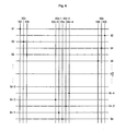
- FIG. 6 is a view illustrating a connection relationship between the vertical scan lines and the horizontal scan lines.
- the first to seventh vertical scan lines VG 1 to VG 7 , the first to eighth vertical data lines D 1 to D 8 , and the common voltage line VCOM are wired in the vertical direction, and the first to third horizontal scan lines G 1 to G 3 are wired.
- Each of the sub-pixels PIX 1 to PIX 16 is defined by one vertical data line, one vertical scan line, and one horizontal scan line. Further, the thin film transistors T 1 to T 16 included in each of the sub-pixel PIX 1 to PIX 16 are connected to the horizontal scan line and the vertical data line disposed at an upper intersection of each of the sub-pixel PIX 1 to PIX 16 . That is, the thin film transistors T 1 to T 16 are disposed in the same way as a top (or a bottom) over all the lines.
- one vertical data line and one vertical scan line are wired so as to pass between the sub-pixels adjacent in right and left direction.
- the common voltage line VCOM may be wired to be included between the sub-pixels adjacent in the right and left direction.
- one horizontal scan line is wired so as to pass between the sub-pixels adjacent in an up and down direction.
- the first sub-pixel PIX 1 is defined by the first vertical data line D 1 , the first vertical scan line VG 1 , and the first horizontal scan line G 1 . Further, the first thin film transistor T 1 included in the first sub-pixel PIX 1 is connected to the first vertical data line D 1 and the first horizontal scan line G 1 .
- the second to sixteenth sub pixels PIX 2 to PIX 16 are defined by the lines passing in the vertical and horizontal directions and are connected to the lines disposed at the intersection thereof.
- the first to third vertical scan lines VG 1 to VG 3 , the first to fifth vertical data lines D 1 to D 5 , and the common voltage line VCOM are wired in the vertical direction, and the first to fifth horizontal scan lines G 1 to G 5 are wired.
- Each of the sub-pixels PIX 1 to PIX 16 is defined by one vertical data line, one vertical scan line, and one horizontal scan line. Further, the thin film transistors T 1 to T 16 included in each of the sub-pixel PIX 1 to PIX 16 are connected to the horizontal scan line and the vertical data line disposed at the upper or lower intersection of each of the sub-pixel PIX 1 to PIX 16 . That is, the thin film transistors T 1 to T 16 are alternately disposed at the top and bottom for each line.
- one vertical data line or one vertical scan line is wired so as to pass between the sub-pixels adjacent in the right and left direction.
- the common voltage line VCOM may be wired to be included between the sub-pixels adjacent in the right and left direction.
- one or two horizontal scan lines are wired so as to pass between the sub-pixels adjacent in the up and down direction.
- the region in which one horizontal scan line is wired may be defined as the uppermost or undermost region of the liquid crystal display panel, and the region in which two horizontal scan lines is wired may be defined as an inner region of the uppermost or undermost region of the liquid crystal display panel.
- the first sub-pixel PIX 1 is defined by the first vertical data line D 1 disposed at the left side thereof, the first vertical scan line VG 1 disposed at the right side thereof, and the first horizontal scan line G 1 disposed at the top thereof. Further, the first thin film transistor T 1 included in the first sub-pixel PIX 1 is connected to the first vertical data line D 1 disposed at the left side thereof and the first horizontal scan line G 1 disposed at the top thereof.
- the second sub-pixel PIX 2 adjacent to the first sub-pixel PIX 1 is defined by the first vertical scan line VG 1 disposed at the left side thereof, the second vertical data line D 2 disposed at the right side thereof, and the second horizontal scan line G 2 disposed at the bottom thereof.
- the second thin film transistor T 2 included in the second sub-pixel PIX 2 is connected to the first vertical data line D 1 disposed at the left side thereof and the second horizontal scan line G 2 disposed at the bottom thereof.
- the third to eighth sub pixels PIX 3 to PIX 18 are defined by the lines passing in the vertical and horizontal directions and are connected to the lines disposed at the intersection thereof.
- the ninth sub-pixel PIX 9 is defined by the first vertical data line D 1 disposed at the left side thereof, the first vertical scan line VG 1 disposed at the right side thereof, and the third horizontal scan line G 3 disposed at the top thereof. Further, the ninth thin film transistor T 9 included in the ninth sub-pixel PIX 9 is connected to the second vertical data line D 2 disposed at the right side thereof and the third horizontal scan line G 3 disposed at the top thereof.
- the tenth sub-pixel PIX 10 adjacent to the ninth sub-pixel PIX 9 is defined by the first vertical scan line VG 1 disposed at the left side thereof, the second vertical data line D 2 disposed at the right side thereof, and the fourth horizontal scan line G 4 disposed at the bottom thereof. Further, the tenth thin film transistor T 10 included in the tenth sub-pixel PIX 10 is connected to the second vertical data line D 2 disposed at the right side thereof and the fourth horizontal scan line G 4 disposed at the bottom thereof.
- the eleventh to sixteenth sub pixels PIX 11 to PIX 16 are defined by the lines passing in the vertical and horizontal directions and are connected to the lines disposed at the intersections thereof.
- a disposition relationship of the vertical lines including the vertical data lines D 1 to D 8 , the vertical scan lines VG 1 to VG 7 , and the vertical common voltage line VCOM and the horizontal lines including the horizontal scan lines G 1 to G 5 have been described with reference to the pixel array shown in FIGS. 4 and 5 .
- the disposition relationship between the vertical and horizontal lines may be variously changed in design according to the structure of the sub-pixel configuring the pixel array, but is not limited thereto.
- the structure using the vertical and horizontal scan lines may have the resistance higher than that of the structure of the scan line according to the related art.
- positions which the horizontal scan lines and the horizontal san lines are connected to each other may be formed as shown in FIG. 6 .
- the portion shown as a dot line in FIG. 6 means a contact hole that serves to electrically connect the horizontal scan line to the horizontal scan line.
- the vertical scan lines VG 1 , VG 3 , . . . VGn- 1 disposed at the left side of the liquid crystal display panel PNL are connected to an odd-numbered horizontal scan lines G 1 , G 3 , . . . Gn- 1 , respectively, and the vertical gate lines VG 2 , VG 4 , . . . VGn disposed at the right side of the liquid crystal display panel PNL are connected to an even-numbered horizontal scan lines G 2 , G 4 , . . . Gn, respectively.
- Gn may be positioned closely at the center of the liquid crystal display panel PNL as distance from the driver increases. Therefore, when the contact holes for electrically connecting the vertical scan lines VG 1 , VG 2 , . . . VGn to the horizontal scan lines G 1 , G 2 , . . . Gn are connected by a virtual line, it is possible to have a V-shape.
- FIG. 7 is a plan view illustrating a sub-pixel according to a first embodiment of the present invention
- FIG. 8 is a cross-sectional view of a region taken along line A 1 -A 2 illustrated in FIG. 7
- FIG. 9 is a cross-sectional view of a region taken along line B 1 -B 2 illustrated in FIG. 7 .
- 1n-1 sub-pixel PIXn- 1 and n sub-pixel PIXn represent the structure formed based on the pixel array shown in FIG. 4 .
- the 1 n- 1 sub pixel PIXn- 1 is defined by n- 1 vertical data line Dn- 1 , n- 1 vertical scan line VGn- 1 , and n horizontal scan line Gn.
- the n sub-pixel PIXn is defined by the n vertical data line Dn, the n vertical scan line VGn, and the n horizontal scan line Gn.
- the n- 1 vertical data line Dn- 1 and n- 1 vertical scan line VGn- 1 and the n vertical data line Dn and n vertical scan line VGn may be wired to make pairs.
- the n vertical data line Dn and the n vertical scan line VGn are disposed in a vertical space vertically dividing a region between the 1 n- 1 sub-pixel PIXn- 1 and the n sub-pixel PIXn.
- the n horizontal scan line Gn is disposed in a horizontal space horizontally dividing a region between the 1 n- 1 sub pixel PIXn- 1 or the n sub-pixel PIXn and the sub-pixels that exist in a next line.
- the n vertical data line Dn and the n horizontal scan line Gn are electrically connected by the contact hole CH disposed in the vertical space vertically dividing the region between the 1 n- 1 sub-pixel PIXn- 1 and the n sub-pixel PIXn.
- the thin film transistor TFT included in the 1 n- 1 sub-pixel PIXn- 1 and the n sub-pixel PIXn may be formed in the various methods, the detailed description thereof replaces with the above-mentioned electrical connection relationship, and the structural description thereof will be omitted.
- the vertical scan line As described above, when signal interference between the pixel electrode and the vertical scan line occurs, a parasitic capacitance between the pixel electrode and the vertical scan line is formed.
- the parasitic capacitance between the pixel electrode and the vertical scan line is formed, the vertical space becomes dark compared with other region and thus, a dim phenomenon in a vertical direction is generated.
- a shield electrode for shielding the signal interference between the pixel electrode and the vertical scan line is formed in the vertical space in which the vertical scan line is formed.
- the method of forming the shield electrode is as follows.
- a first insulating film 111 is formed on the lower substrate 110 .
- the first insulating film 111 may be made of a silicon oxide film SiOx or a silicon nitride film SiNx.
- the horizontal scan line 113 disposed in the vertical space is formed on the first insulating film 111 .
- the horizontal scan line 113 may be at least one selected from a group consisting of molybdenum (Mo), aluminum (Al), chrome (Cr), gold (Au), titanium (Ti), nickel (Ni), and copper (Cu), or an alloy thereof. Further, the horizontal scan line 113 may be formed of the single layer or the multi-layer.
- the horizontal scan line 113 corresponds to Gn of FIG. 7 .
- a second insulating film 115 is formed on the horizontal scan line 113 .
- the second insulating film 113 may be made of a silicon oxide film SiOx or a silicon nitride film SiNx.
- the contact hole CH exposing a portion of the horizontal scan line 113 disposed in the vertical space is formed on the second insulating film 113 .
- the vertical scan line 119 disposed in the vertical space is formed on the second insulating film 113 .
- the vertical scan line 119 may be at least one selected from a group consisting of molybdenum (Mo), aluminum (Al), chrome (Cr), gold (Au), titanium (Ti), nickel (Ni), and copper (Cu), or an alloy thereof.
- the horizontal scan line 113 may be formed of the single layer or the multi-layer.
- the vertical scan line 119 is electrically connected with the horizontal scan line 113 formed at the lower portion thereof through the contact hole CH disposed in the vertical space.
- the vertical scan line 119 corresponds to VGn of FIG. 7 .
- a third insulating film 120 is formed on the vertical scan line 119 .
- the third insulating film 120 is selected in an organic film, an inorganic film, or an organic-inorganic composite film, capable of planarizing a surface such as polyacryl.
- a transparent electrode 122 is formed on the third insulating film 120 .
- the transparent electrode 122 may be made of a transparent conductive film such as indium tin oxide (ITO), indium zinc oxide (IZO), indium tin zinc oxide (ITZO), zinc oxide (ZnO), indium gallium zinc oxide (IGZO), grapheme, or the like.
- the transparent electrode 122 serves as he common electrode and the shield electrode. That is, the transparent electrode 122 is the common electrode which is formed integrally with the shield electrode.
- a fourth insulating film 124 is formed on the transparent electrode 122 .
- the fourth insulating film 124 may be made of a silicon oxide film SiOx or a silicon nitride film SiNx.
- a first insulating film 111 is formed on the lower substrate 110 .
- the vertical data line 112 disposed in the vertical space is formed on the first insulating film 111 .
- the second insulating film 115 is formed on the vertical data line 112 .
- the vertical scan line 119 disposed in the vertical space is formed on the second insulating film 115 .
- the third insulating film 120 is formed on the vertical scan line 119 .
- the transparent electrode 122 is formed on the third insulating film 120 .
- the transparent electrode 122 is formed over entire surface of the third insulating film 120 .
- the transparent electrode 122 serves as he common electrode and the shield electrode.
- the fourth insulating film 124 is formed on the transparent electrode 122 .
- the pixel electrodes 126 are formed on the third insulating film 124 .
- the pixel electrodes 126 are separately disposed in the region of the n- 1 and n sub-pixels PIXn- 1 and PIXn.
- the pixel electrode 126 may be configured to be divided into a plurality of pixel electrodes so as to have a ( ⁇ ) shape in a transmission region as shown in FIG. 7 .
- the n- 1 vertical data line Dn- 1 and n- 1 vertical scan line VGn- 1 and the n vertical data line Dn and n vertical scan line VGn may be wired so as to have the ( ⁇ ) shape.
- the reference numeral 130 represents a black matrix formed on the upper substrate
- a width of the vertical space may correspond to the width of the black matrix 130 in the vertical direction.
- FIGS. 10 a and 10 b are cross-sectional views for comparing explaining a comparative example and a first embodiment.
- the comparative example shown in FIG. 10A has a structure similar to those of the first embodiment shown in FIG. 10B except that the transparent electrode 122 is formed on the lower substrate 110 and the shield electrode does not exist between the vertical scan line 119 and the pixel electrode 126 .
- the shield electrode does not exist between the vertical scan line 119 and the pixel electrode 126 .
- the parasitic capacitance Cg is formed by the signal interference between the vertical scan line 119 and the pixel electrode 126 .
- the parasitic capacitance between the pixel electrode 126 and the vertical scan line 119 is formed, the vertical space becomes dark compared with other region and thus, the dim phenomenon in a vertical direction is generated.
- the transparent electrode 122 to serve as the shield electrode is formed between the vertical scan line 119 and the pixel electrode 126 .
- the signal interference between the vertical scan line 119 and the pixel electrode 126 is shielded by the common voltage which is applied to the transparent electrode 122 , such that the parasitic capacitance Cg is not formed and an occurrence of parasitic capacitance is suppressed. Therefore, with the first embodiment (b), the parasitic capacitance Cg is not formed and the occurrence of parasitic capacitance is suppressed, thereby making it possible to improve or prevent the dim phenomenon in the vertical direction.
- the signal interference between the vertical scan line 119 and the pixel electrode 126 is shielded, thereby making it possible to adopt a driving system that supplies to overlap the scan signal.
- a stacked structure of the liquid crystal display panel is not limited to the structure as described above and may be variously implemented.
- the embodiment of the present invention will be described by dividing for each cross-sectional structure of the sub-pixel.
- FIG. 11 is a cross-sectional view of a region taken along line B 1 -B 2 illustrated in FIG. 7 according to a second embodiment of the present invention.
- a first insulating film 111 is formed on the lower substrate 110 .
- the vertical data line 112 disposed in the vertical space is formed on the first insulating film 111 .
- the second insulating film 115 is formed on the vertical data line 112 .
- the vertical scan line 119 disposed in the vertical space is formed on the second insulating film 115 .
- the third insulating film 120 is formed on the vertical scan line 119 .
- a first transparent electrode 122 a and a second transparent electrode 122 b are separated and formed on the third insulating film 120 .
- the first transparent electrode 122 a is formed to be separately disposed in the region of the sub-pixels and it becomes the common electrode.
- the second transparent electrode 122 b is formed to be disposed in the vertical space, and it becomes the shield electrode.
- the second transparent electrode 122 b which serves as the shield electrode is connected to the line for supplying the ground voltage or the voltage between the positive and negative voltages.
- the fourth insulating film 124 is formed on the first and second transparent electrodes 122 a and 122 b .
- the pixel electrodes 126 are formed on the fourth insulating film 124 .
- the pixel electrodes 126 are separately disposed in the region of the n- 1 and n sub-pixels PIXn- 1 and PIXn.
- the pixel electrode 126 may be configured to be divided into a plurality of pixel electrodes so as to have the ( ⁇ ) shape in the transmission region as shown in FIG. 7 .
- the n- 1 vertical data line Dn- 1 and n- 1 vertical scan line VGn- 1 and the n vertical data line Dn and n vertical scan line VGn may be wired so as to have the ( ⁇ ) shape.
- the reference numeral 130 represents a black matrix formed on the upper substrate
- a width of the vertical space may correspond to the width of the black matrix 130 in the vertical direction.
- the first transparent electrode 122 a which serves as the common electrode and the second transparent electrode 122 b which serves as the shield electrode are formed to be electrically separated from each other.
- the common voltage supplied to the common electrode may swing in the positive and negative voltages according to a driving type (for example, a line inversion type) of the liquid crystal display panel.
- a driving type for example, a line inversion type
- the second embodiment may apply to the structure in which the common voltage swings such as the line inversion type.
- FIG. 12 is a cross-sectional view of a region taken along line B 1 -B 2 illustrated in FIG. 7 according to a third embodiment of the present invention.
- the transparent electrode 122 which are separately disposed in the region of the n- 1 and n sub-pixels PIXn- 1 and PIXn to become the common electrode are formed on the lower substrate 110 .
- the first insulating film 111 is formed on the transparent electrode 122 .
- the vertical data line 112 disposed in the vertical space is formed on the first insulating film 111 .
- the second insulating film 115 is formed on the vertical data line 112 .
- the vertical scan line 119 disposed in the vertical space is formed on the second insulating film 115 .
- the third insulating film 120 is formed on the vertical scan line 119 .
- the shield electrode 125 disposed in the vertical space is formed on the third insulating film 120 .
- the shield electrode 125 is connected to the line for supplying the ground voltage or the voltage between the positive and negative voltages.
- the fourth insulating film 124 is formed on the shield electrode 125 .
- the pixel electrodes 126 are formed on the fourth insulating film 124 .
- the pixel electrodes 126 are separately disposed in the region of the n- 1 and n sub-pixels PIXn- 1 and PIXn.
- the pixel electrode 126 may be disposed to be divided into a plurality of pixel electrodes so as to have a ( ⁇ ) shape in th transmission region as shown in FIG. 7 .
- the n- 1 vertical data line Dn- 1 and n- 1 vertical scan line VGn- 1 and the n vertical data line Dn and n vertical scan line VGn may be wired so as to have the ( ⁇ ) shape.
- the reference numeral 130 represents a black matrix formed on the upper substrate
- a width of the vertical space may correspond to the width of the black matrix 130 in the vertical direction.
- the transparent electrode, which becomes the common electrode, and the shield electrode 125 are formed to be separated in layers different from each other.
- the structure is to apply the shield electrode 125 to the comparative example shown in FIG. 10A
- FIG. 13 is a cross-sectional view of a region taken along line B 1 -B 2 illustrated in FIG. 7 according to a fourth embodiment of the present invention.
- a first insulating film 111 is formed on the lower substrate 110 .
- the vertical data line 112 disposed in the vertical space is formed on the first insulating film 111 .
- the second insulating film 115 is formed on the vertical data line 112 .
- the vertical scan line 119 disposed in the vertical space is formed on the second insulating film 115 .
- the third insulating film 120 is formed on the vertical scan line 119 .
- the transparent electrodes 122 which become the common electrode are formed to be separately disposed in the region of the sub-pixels on the third insulating film 120 .
- the fourth insulating film 124 is formed on the transparent electrode 122 .
- the shield electrode 125 disposed in the vertical space is formed on the fourth insulating film 124 .
- the shield electrode 125 is connected to the line for supplying the common voltage, the ground voltage or the voltage between the positive and negative voltages.
- the pixel electrodes 126 are formed on the fourth insulating film 124 .
- the pixel electrodes 126 are separately disposed in the region of the n- 1 and n sub-pixels PIXn- 1 and PIXn.
- the pixel electrode 126 may be configured to be divided into a plurality of pixel electrodes so as to have a ( ⁇ ) shape in the transmission region as shown in FIG. 7 .
- the n- 1 vertical data line Dn- 1 and n- 1 vertical scan line VGn- 1 and the n vertical data line Dn and n vertical scan line VGn may be wired so as to have the ( ⁇ ) shape.
- the reference numeral 130 represents a black matrix formed on the upper substrate
- a width of the vertical space may correspond to the width of the black matrix 130 in the vertical direction.
- the shield electrode 125 and the pixel electrode 126 are formed of the same transparent conductive film and are patterned, such that the two electrodes may be separated from each other, thereby making it possible to shield the signal interference between the vertical scan line and the pixel electrode without an additional process.
- FIG. 14 is a cross-sectional view of a region taken along line B 1 -B 2 illustrated in FIG. 7 according to a fifth embodiment of the present invention.
- the transparent electrodes 122 which are separately disposed in the region of the n- 1 and n sub-pixels PIXn- 1 and PIXn to become the common electrode are formed on the lower substrate 110 .
- the first insulating film 111 is formed on the transparent electrode 122 .
- the vertical data line 112 disposed in the vertical space is formed on the first insulating film 111 .
- the second insulating film 115 is formed on the vertical data line 112 .
- the vertical scan line 119 disposed in the vertical space is formed on the second insulating film 115 .
- the third insulating film 120 is formed on the vertical scan line 119 .
- the fourth insulating film 124 is formed on the third insulating film 120 .
- the shield electrode 125 disposed in the vertical space is formed on the fourth insulating film 124 .
- the shield electrode 125 is connected to the line for supplying the common voltage, the ground voltage or the voltage between the positive and negative voltages.
- the pixel electrodes 126 are formed on the fourth insulating film 124 .
- the pixel electrodes 126 are separately disposed in the region of the n- 1 and n sub-pixels PIXn- 1 and PIXn.
- the pixel electrode 126 may be configured to be divided into a plurality of pixel electrodes so as to have a ( ⁇ ) shape in the transmission region as shown in FIG. 7 .
- the n- 1 vertical data line Dn- 1 and n- 1 vertical scan line VGn- 1 and the n vertical data line Dn and n vertical scan line VGn may be wired so as to have the ( ⁇ ) shape.
- the reference numeral 130 represents a black matrix formed on the upper substrate
- a width of the vertical space may correspond to the width of the black matrix 130 in the vertical direction.
- the transparent electrode 122 which becomes the common electrode, and the shield electrode 125 are formed to be separated in layers different from each other.
- the structure is to apply the shield electrode 125 to the comparative example shown in FIG. 10A , the shield electrode 125 and the pixel electrode 126 are formed of the same transparent conductive film and are patterned, such that the two electrodes may be separated from each other, thereby making it possible to provide a convenience of process compared to the third embodiment.
- the dim phenomenon that is generated in the vertical direction by the signal interference between the vertical scan line and the pixel electrode is improved or removed, thereby making it possible to implement the narrow bezel.
- the present invention can apply effectively to the liquid crystal display panel of various structures having the vertical scan line.
- the present invention can maintain the shielding ability between the vertical scan line and the pixel electrode.
Applications Claiming Priority (2)
| Application Number | Priority Date | Filing Date | Title |
|---|---|---|---|
| KR1020130072928A KR102033619B1 (ko) | 2013-06-25 | 2013-06-25 | 표시장치 |
| KR10-2013-0072928 | 2013-06-25 |
Publications (2)
| Publication Number | Publication Date |
|---|---|
| US20140375534A1 US20140375534A1 (en) | 2014-12-25 |
| US9697786B2 true US9697786B2 (en) | 2017-07-04 |
Family
ID=52110467
Family Applications (1)
| Application Number | Title | Priority Date | Filing Date |
|---|---|---|---|
| US14/310,581 Active 2034-10-11 US9697786B2 (en) | 2013-06-25 | 2014-06-20 | Display device |
Country Status (3)
| Country | Link |
|---|---|
| US (1) | US9697786B2 (zh) |
| KR (1) | KR102033619B1 (zh) |
| CN (1) | CN104252068B (zh) |
Families Citing this family (34)
| Publication number | Priority date | Publication date | Assignee | Title |
|---|---|---|---|---|
| KR101325325B1 (ko) * | 2012-11-30 | 2013-11-08 | 엘지디스플레이 주식회사 | 액정표시장치와 그 제조 방법 |
| KR102034112B1 (ko) * | 2013-06-19 | 2019-10-21 | 엘지디스플레이 주식회사 | 액정 디스플레이 장치와 이의 구동방법 |
| WO2015092944A1 (ja) * | 2013-12-19 | 2015-06-25 | パナソニック液晶ディスプレイ株式会社 | 表示装置及び表示装置の製造方法 |
| CN103744239A (zh) * | 2013-12-26 | 2014-04-23 | 深圳市华星光电技术有限公司 | 一种内嵌式触控阵列基板结构 |
| KR102228269B1 (ko) * | 2014-07-09 | 2021-03-17 | 삼성디스플레이 주식회사 | 표시 기판 및 이의 제조 방법 |
| JP2016071083A (ja) * | 2014-09-29 | 2016-05-09 | パナソニック液晶ディスプレイ株式会社 | 表示装置及び駆動回路 |
| CN104503633B (zh) * | 2015-01-26 | 2018-07-06 | 京东方科技集团股份有限公司 | 一种内嵌式触摸屏、其驱动方法及显示装置 |
| CN104656324A (zh) * | 2015-03-17 | 2015-05-27 | 京东方科技集团股份有限公司 | 阵列基板及其制作方法以及显示装置 |
| CN104793416B (zh) * | 2015-04-14 | 2018-02-16 | 京东方科技集团股份有限公司 | 一种阵列基板及其制作方法和显示面板 |
| CN105068340B (zh) | 2015-09-21 | 2018-11-06 | 京东方科技集团股份有限公司 | 阵列基板、显示装置及其制作方法 |
| CN105185791A (zh) | 2015-09-28 | 2015-12-23 | 京东方科技集团股份有限公司 | 阵列基板及其制作方法、显示装置 |
| KR102587647B1 (ko) * | 2016-05-04 | 2023-10-11 | 삼성디스플레이 주식회사 | 액정 표시 장치 및 그 제조방법 |
| TWI579825B (zh) * | 2016-08-29 | 2017-04-21 | 友達光電股份有限公司 | 顯示面板及其驅動方法 |
| JP6743594B2 (ja) * | 2016-09-01 | 2020-08-19 | 凸版印刷株式会社 | 表示装置及び表示方法 |
| KR102553139B1 (ko) * | 2016-10-24 | 2023-07-10 | 엘지디스플레이 주식회사 | 표시장치 |
| KR20180074905A (ko) | 2016-12-23 | 2018-07-04 | 엘지디스플레이 주식회사 | 협 베젤 표시장치 |
| US10950679B1 (en) * | 2017-09-07 | 2021-03-16 | Apple Inc. | Display having vertically driven gate and data paths |
| US10718982B2 (en) * | 2018-03-29 | 2020-07-21 | Panasonic Liquid Crystal Display Co., Ltd. | Liquid crystal display devices |
| CN110085134B (zh) * | 2018-04-18 | 2021-08-27 | 友达光电股份有限公司 | 显示装置 |
| CN108873500A (zh) * | 2018-06-01 | 2018-11-23 | 深圳市华星光电技术有限公司 | 液晶显示面板结构 |
| CN109343286A (zh) * | 2018-11-21 | 2019-02-15 | 武汉华星光电技术有限公司 | 一种液晶显示面板 |
| CN111384082B (zh) * | 2018-12-27 | 2023-01-10 | 武汉华星光电半导体显示技术有限公司 | Oled显示面板 |
| JP7261595B2 (ja) * | 2019-01-31 | 2023-04-20 | トライベイル テクノロジーズ, エルエルシー | 表示装置 |
| KR20210075441A (ko) | 2019-12-13 | 2021-06-23 | 엘지디스플레이 주식회사 | 투명 표시 패널 및 이를 포함하는 투명 표시 장치 |
| US11740519B2 (en) | 2020-01-07 | 2023-08-29 | Samsung Display Co., Ltd. | Display device |
| KR102651717B1 (ko) * | 2020-01-07 | 2024-03-27 | 삼성디스플레이 주식회사 | 표시 장치 |
| CN111258141A (zh) * | 2020-03-06 | 2020-06-09 | Tcl华星光电技术有限公司 | 显示面板、显示装置 |
| KR20210145892A (ko) * | 2020-05-25 | 2021-12-03 | 삼성디스플레이 주식회사 | 표시 장치 |
| CN112255852A (zh) * | 2020-10-23 | 2021-01-22 | 深圳市华星光电半导体显示技术有限公司 | 显示装置及发光面板 |
| CN112365831B (zh) * | 2020-12-02 | 2022-04-08 | 深圳市华星光电半导体显示技术有限公司 | 显示面板 |
| CN112764284A (zh) * | 2021-02-07 | 2021-05-07 | Tcl华星光电技术有限公司 | 阵列基板及显示面板 |
| CN113362750B (zh) * | 2021-05-31 | 2022-04-01 | 长沙惠科光电有限公司 | 阵列基板、显示设备及阵列基板驱动方法 |
| CN113985668A (zh) * | 2021-10-25 | 2022-01-28 | Tcl华星光电技术有限公司 | 像素电路以及其制造方法 |
| CN114171574B (zh) * | 2021-12-08 | 2023-05-09 | 武汉华星光电半导体显示技术有限公司 | 显示面板 |
Citations (6)
| Publication number | Priority date | Publication date | Assignee | Title |
|---|---|---|---|---|
| US20100066967A1 (en) * | 2008-09-18 | 2010-03-18 | Toshiba Mobile Display Co., Ltd. | Liquid crystal display device |
| US20110102309A1 (en) * | 2009-11-05 | 2011-05-05 | Young-Joon Cho | Thin film transistor display panel and method of manufacturing the same |
| CN102456333A (zh) | 2010-10-25 | 2012-05-16 | 精工爱普生株式会社 | 电光装置以及电子设备 |
| US20130113766A1 (en) * | 2011-11-04 | 2013-05-09 | Samsung Display Co., Ltd. | Display apparatus and method of manufacturing the same |
| CN103137616A (zh) | 2011-11-25 | 2013-06-05 | 上海天马微电子有限公司 | Tft阵列基板及其形成方法、显示面板 |
| CN103163671A (zh) | 2011-12-14 | 2013-06-19 | 上海天马微电子有限公司 | 显示面板及其形成方法、液晶显示装置 |
Family Cites Families (1)
| Publication number | Priority date | Publication date | Assignee | Title |
|---|---|---|---|---|
| US20110298785A1 (en) * | 2010-06-02 | 2011-12-08 | Apple Inc. | Gate shielding for liquid crystal displays |
-
2013
- 2013-06-25 KR KR1020130072928A patent/KR102033619B1/ko active IP Right Grant
-
2014
- 2014-06-12 CN CN201410261636.1A patent/CN104252068B/zh active Active
- 2014-06-20 US US14/310,581 patent/US9697786B2/en active Active
Patent Citations (7)
| Publication number | Priority date | Publication date | Assignee | Title |
|---|---|---|---|---|
| US20100066967A1 (en) * | 2008-09-18 | 2010-03-18 | Toshiba Mobile Display Co., Ltd. | Liquid crystal display device |
| US20110102309A1 (en) * | 2009-11-05 | 2011-05-05 | Young-Joon Cho | Thin film transistor display panel and method of manufacturing the same |
| CN102456333A (zh) | 2010-10-25 | 2012-05-16 | 精工爱普生株式会社 | 电光装置以及电子设备 |
| US20130113766A1 (en) * | 2011-11-04 | 2013-05-09 | Samsung Display Co., Ltd. | Display apparatus and method of manufacturing the same |
| CN103137616A (zh) | 2011-11-25 | 2013-06-05 | 上海天马微电子有限公司 | Tft阵列基板及其形成方法、显示面板 |
| US20130314636A1 (en) * | 2011-11-25 | 2013-11-28 | Shanghai Tianma Micro-electronics Co., Ltd. | Tft array substrate and forming method thereof, and display panel |
| CN103163671A (zh) | 2011-12-14 | 2013-06-19 | 上海天马微电子有限公司 | 显示面板及其形成方法、液晶显示装置 |
Non-Patent Citations (1)
| Title |
|---|
| Office Action dated Jul. 14, 2016 for Chinese Application No. 201410261636.1, 20 pages. |
Also Published As
| Publication number | Publication date |
|---|---|
| KR20150000926A (ko) | 2015-01-06 |
| CN104252068B (zh) | 2017-05-03 |
| US20140375534A1 (en) | 2014-12-25 |
| CN104252068A (zh) | 2014-12-31 |
| KR102033619B1 (ko) | 2019-10-18 |
Similar Documents
| Publication | Publication Date | Title |
|---|---|---|
| US9697786B2 (en) | Display device | |
| JP5661156B2 (ja) | 液晶表示装置とその駆動方法 | |
| KR102020938B1 (ko) | 액정표시장치 | |
| EP2743762B1 (en) | Liquid crystal display device | |
| KR102009388B1 (ko) | 액정 디스플레이 장치 | |
| JP4937333B2 (ja) | 液晶表示装置およびその製造方法 | |
| US9691343B2 (en) | Display device comprising display panel with bridge patterns | |
| KR20080007812A (ko) | 터치 스크린 표시 장치 및 그 구동 방법 | |
| KR20110107659A (ko) | 액정표시장치 | |
| KR101966865B1 (ko) | 액정표시장치와 이의 제조방법 | |
| KR102394393B1 (ko) | 표시장치 | |
| GB2489295A (en) | Liquid crystal display device and method of driving the same | |
| US11347340B2 (en) | Display device | |
| KR20140080672A (ko) | 액정 디스플레이 장치 | |
| CN113284413A (zh) | 显示设备 | |
| KR20160012789A (ko) | 액정표시장치 | |
| KR102075355B1 (ko) | 액정표시장치 | |
| KR102222144B1 (ko) | 표시장치 | |
| KR20120002048A (ko) | 액정표시장치와 이의 제조방법 | |
| KR20120041457A (ko) | 액정표시장치 | |
| KR102231043B1 (ko) | 액정표시장치 | |
| KR20180025489A (ko) | 표시장치 |
Legal Events
| Date | Code | Title | Description |
|---|---|---|---|
| AS | Assignment |
Owner name: LG DISPLAY CO., LTD., KOREA, REPUBLIC OF Free format text: ASSIGNMENT OF ASSIGNORS INTEREST;ASSIGNORS:LEE, SEEUNG;PARK, CHANSOO;RYOO, SEUNGSEOK;REEL/FRAME:033150/0140 Effective date: 20140602 |
|
| STCF | Information on status: patent grant |
Free format text: PATENTED CASE |
|
| MAFP | Maintenance fee payment |
Free format text: PAYMENT OF MAINTENANCE FEE, 4TH YEAR, LARGE ENTITY (ORIGINAL EVENT CODE: M1551); ENTITY STATUS OF PATENT OWNER: LARGE ENTITY Year of fee payment: 4 |