US9494869B2 - Lithographic apparatus and device manufacturing method - Google Patents
Lithographic apparatus and device manufacturing method Download PDFInfo
- Publication number
- US9494869B2 US9494869B2 US14/357,530 US201214357530A US9494869B2 US 9494869 B2 US9494869 B2 US 9494869B2 US 201214357530 A US201214357530 A US 201214357530A US 9494869 B2 US9494869 B2 US 9494869B2
- Authority
- US
- United States
- Prior art keywords
- frame
- movable frame
- imbalance
- movable
- frames
- Prior art date
- Legal status (The legal status is an assumption and is not a legal conclusion. Google has not performed a legal analysis and makes no representation as to the accuracy of the status listed.)
- Expired - Fee Related, expires
Links
Images


Classifications
-
- G—PHYSICS
- G03—PHOTOGRAPHY; CINEMATOGRAPHY; ANALOGOUS TECHNIQUES USING WAVES OTHER THAN OPTICAL WAVES; ELECTROGRAPHY; HOLOGRAPHY
- G03F—PHOTOMECHANICAL PRODUCTION OF TEXTURED OR PATTERNED SURFACES, e.g. FOR PRINTING, FOR PROCESSING OF SEMICONDUCTOR DEVICES; MATERIALS THEREFOR; ORIGINALS THEREFOR; APPARATUS SPECIALLY ADAPTED THEREFOR
- G03F7/00—Photomechanical, e.g. photolithographic, production of textured or patterned surfaces, e.g. printing surfaces; Materials therefor, e.g. comprising photoresists; Apparatus specially adapted therefor
- G03F7/70—Microphotolithographic exposure; Apparatus therefor
- G03F7/70216—Mask projection systems
- G03F7/70258—Projection system adjustments, e.g. adjustments during exposure or alignment during assembly of projection system
-
- G—PHYSICS
- G03—PHOTOGRAPHY; CINEMATOGRAPHY; ANALOGOUS TECHNIQUES USING WAVES OTHER THAN OPTICAL WAVES; ELECTROGRAPHY; HOLOGRAPHY
- G03F—PHOTOMECHANICAL PRODUCTION OF TEXTURED OR PATTERNED SURFACES, e.g. FOR PRINTING, FOR PROCESSING OF SEMICONDUCTOR DEVICES; MATERIALS THEREFOR; ORIGINALS THEREFOR; APPARATUS SPECIALLY ADAPTED THEREFOR
- G03F7/00—Photomechanical, e.g. photolithographic, production of textured or patterned surfaces, e.g. printing surfaces; Materials therefor, e.g. comprising photoresists; Apparatus specially adapted therefor
- G03F7/70—Microphotolithographic exposure; Apparatus therefor
- G03F7/70216—Mask projection systems
- G03F7/70275—Multiple projection paths, e.g. array of projection systems, microlens projection systems or tandem projection systems
-
- G—PHYSICS
- G03—PHOTOGRAPHY; CINEMATOGRAPHY; ANALOGOUS TECHNIQUES USING WAVES OTHER THAN OPTICAL WAVES; ELECTROGRAPHY; HOLOGRAPHY
- G03F—PHOTOMECHANICAL PRODUCTION OF TEXTURED OR PATTERNED SURFACES, e.g. FOR PRINTING, FOR PROCESSING OF SEMICONDUCTOR DEVICES; MATERIALS THEREFOR; ORIGINALS THEREFOR; APPARATUS SPECIALLY ADAPTED THEREFOR
- G03F7/00—Photomechanical, e.g. photolithographic, production of textured or patterned surfaces, e.g. printing surfaces; Materials therefor, e.g. comprising photoresists; Apparatus specially adapted therefor
- G03F7/70—Microphotolithographic exposure; Apparatus therefor
- G03F7/70216—Mask projection systems
- G03F7/70358—Scanning exposure, i.e. relative movement of patterned beam and workpiece during imaging
- G03F7/70366—Rotary scanning
-
- G—PHYSICS
- G03—PHOTOGRAPHY; CINEMATOGRAPHY; ANALOGOUS TECHNIQUES USING WAVES OTHER THAN OPTICAL WAVES; ELECTROGRAPHY; HOLOGRAPHY
- G03F—PHOTOMECHANICAL PRODUCTION OF TEXTURED OR PATTERNED SURFACES, e.g. FOR PRINTING, FOR PROCESSING OF SEMICONDUCTOR DEVICES; MATERIALS THEREFOR; ORIGINALS THEREFOR; APPARATUS SPECIALLY ADAPTED THEREFOR
- G03F7/00—Photomechanical, e.g. photolithographic, production of textured or patterned surfaces, e.g. printing surfaces; Materials therefor, e.g. comprising photoresists; Apparatus specially adapted therefor
- G03F7/70—Microphotolithographic exposure; Apparatus therefor
- G03F7/70383—Direct write, i.e. pattern is written directly without the use of a mask by one or multiple beams
- G03F7/704—Scanned exposure beam, e.g. raster-, rotary- and vector scanning
-
- G—PHYSICS
- G03—PHOTOGRAPHY; CINEMATOGRAPHY; ANALOGOUS TECHNIQUES USING WAVES OTHER THAN OPTICAL WAVES; ELECTROGRAPHY; HOLOGRAPHY
- G03F—PHOTOMECHANICAL PRODUCTION OF TEXTURED OR PATTERNED SURFACES, e.g. FOR PRINTING, FOR PROCESSING OF SEMICONDUCTOR DEVICES; MATERIALS THEREFOR; ORIGINALS THEREFOR; APPARATUS SPECIALLY ADAPTED THEREFOR
- G03F7/00—Photomechanical, e.g. photolithographic, production of textured or patterned surfaces, e.g. printing surfaces; Materials therefor, e.g. comprising photoresists; Apparatus specially adapted therefor
- G03F7/70—Microphotolithographic exposure; Apparatus therefor
- G03F7/70483—Information management; Active and passive control; Testing; Wafer monitoring, e.g. pattern monitoring
- G03F7/7055—Exposure light control in all parts of the microlithographic apparatus, e.g. pulse length control or light interruption
- G03F7/70558—Dose control, i.e. achievement of a desired dose
-
- G—PHYSICS
- G03—PHOTOGRAPHY; CINEMATOGRAPHY; ANALOGOUS TECHNIQUES USING WAVES OTHER THAN OPTICAL WAVES; ELECTROGRAPHY; HOLOGRAPHY
- G03F—PHOTOMECHANICAL PRODUCTION OF TEXTURED OR PATTERNED SURFACES, e.g. FOR PRINTING, FOR PROCESSING OF SEMICONDUCTOR DEVICES; MATERIALS THEREFOR; ORIGINALS THEREFOR; APPARATUS SPECIALLY ADAPTED THEREFOR
- G03F7/00—Photomechanical, e.g. photolithographic, production of textured or patterned surfaces, e.g. printing surfaces; Materials therefor, e.g. comprising photoresists; Apparatus specially adapted therefor
- G03F7/70—Microphotolithographic exposure; Apparatus therefor
- G03F7/708—Construction of apparatus, e.g. environment aspects, hygiene aspects or materials
- G03F7/70808—Construction details, e.g. housing, load-lock, seals or windows for passing light in or out of apparatus
- G03F7/70816—Bearings
-
- G—PHYSICS
- G03—PHOTOGRAPHY; CINEMATOGRAPHY; ANALOGOUS TECHNIQUES USING WAVES OTHER THAN OPTICAL WAVES; ELECTROGRAPHY; HOLOGRAPHY
- G03F—PHOTOMECHANICAL PRODUCTION OF TEXTURED OR PATTERNED SURFACES, e.g. FOR PRINTING, FOR PROCESSING OF SEMICONDUCTOR DEVICES; MATERIALS THEREFOR; ORIGINALS THEREFOR; APPARATUS SPECIALLY ADAPTED THEREFOR
- G03F7/00—Photomechanical, e.g. photolithographic, production of textured or patterned surfaces, e.g. printing surfaces; Materials therefor, e.g. comprising photoresists; Apparatus specially adapted therefor
- G03F7/70—Microphotolithographic exposure; Apparatus therefor
- G03F7/708—Construction of apparatus, e.g. environment aspects, hygiene aspects or materials
- G03F7/70858—Environment aspects, e.g. pressure of beam-path gas, temperature
- G03F7/709—Vibration, e.g. vibration detection, compensation, suppression or isolation
-
- G—PHYSICS
- G03—PHOTOGRAPHY; CINEMATOGRAPHY; ANALOGOUS TECHNIQUES USING WAVES OTHER THAN OPTICAL WAVES; ELECTROGRAPHY; HOLOGRAPHY
- G03F—PHOTOMECHANICAL PRODUCTION OF TEXTURED OR PATTERNED SURFACES, e.g. FOR PRINTING, FOR PROCESSING OF SEMICONDUCTOR DEVICES; MATERIALS THEREFOR; ORIGINALS THEREFOR; APPARATUS SPECIALLY ADAPTED THEREFOR
- G03F7/00—Photomechanical, e.g. photolithographic, production of textured or patterned surfaces, e.g. printing surfaces; Materials therefor, e.g. comprising photoresists; Apparatus specially adapted therefor
- G03F7/70—Microphotolithographic exposure; Apparatus therefor
- G03F7/70383—Direct write, i.e. pattern is written directly without the use of a mask by one or multiple beams
- G03F7/70391—Addressable array sources specially adapted to produce patterns, e.g. addressable LED arrays
Definitions
- the present invention relates to a lithographic or exposure apparatus and a method for manufacturing a device.
- a lithographic apparatus is a machine that applies a desired pattern onto a substrate or part of a substrate.
- a lithographic apparatus may be used, for example, in the manufacture of integrated circuits (ICs), flat panel displays and other devices or structures having fine features.
- a patterning device which may be referred to as a mask or a reticle, may be used to generate a circuit pattern corresponding to an individual layer of the IC, flat panel display, or other device).
- This pattern may be transferred on (part of) the substrate (e.g. silicon wafer or a glass plate), e.g. via imaging onto a layer of radiation-sensitive material (resist) provided on the substrate.
- an exposure apparatus is a machine that uses a radiation beam in forming a desired pattern on or in a substrate (or a part thereof).
- the patterning device may be used to generate other patterns, for example a color filter pattern, or a matrix of dots.
- the patterning device may comprise a patterning array that comprises an array of individually controllable elements that generate the circuit or other applicable pattern.
- a maskless system includes a programmable patterning device (e.g., a spatial light modulator, a contrast device, etc.).
- the programmable patterning device is programmed (e.g., electronically or optically) to form the desired patterned beam using the array of individually controllable elements.
- Types of programmable patterning devices include micro-mirror arrays, liquid crystal display (LCD) arrays, grating light valve arrays, arrays of self-emissive contrast devices and the like.
- a programmable patterning device could also be formed from an electro-optical deflector, configured for example to move spots of radiation projected onto the substrate or to intermittently direct a radiation beam away from the substrate, for example to a radiation beam absorber. In either such arrangement, the radiation beam may be continuous.
- an exposure apparatus comprising:
- a projection system configured to project a plurality of radiation beams onto a target
- a movable frame that is at least rotatable around an axis
- an actuator system configured to displace the movable frame to an axis away from an axis corresponding to the geometric center of the movable frame and to cause the frame to rotate around an axis through the center of mass of the frame.
- an exposure apparatus comprising:
- a projection system configured to project a plurality of radiation beams onto a target
- a movable frame that is at least rotatable around an axis
- a controller of the actuator system configured to feedforward a gyroscopic compensation.
- an exposure apparatus comprising:
- a projection system configured to project a plurality of radiation beams onto a target
- a movable frame that is at least rotatable around an axis
- an actuator system to cause the frame to rotate relative to a part that is substantially stationary relative to the frame and having an actuator to cause the frame to displace relative to the part;
- reaction mass movably attached to the part, the reaction mass having a portion of the actuator.
- an exposure apparatus comprising:
- a projection system configured to project a plurality of radiation beams onto a target
- a movable frame that is at least rotatable around an axis
- an actuator system to cause the frame to rotate, the actuator system comprising at least two motors around the axis;
- each of the plurality of sensors located at an angular position that substantially bisects the angular positions of two adjacent motors.
- an exposure apparatus comprising:
- a projection system configured to project a plurality of radiation beams onto a target
- a movable frame that is at least rotatable around an axis
- an actuator system to cause the frame to rotate, the actuator system comprising a first set of at least two motors about the axis and a second set of at least two motors about the axis and below the first set, wherein the second set is rotated about the axis with respect to the first set.
- an exposure apparatus comprising:
- a projection system configured to project a plurality of radiation beams onto a target
- a movable frame that is at least rotatable around an axis
- a sensor system to measure the frame in a substantially tangential direction.
- an exposure apparatus comprising:
- a projection system configured to project a plurality of radiation beams onto a target
- a movable frame that is at least rotatable around an axis
- a controller to adjust a position of the movable frame to compensate at least in part for imbalance of the movable frame or imbalance of another movable frame.
- an exposure apparatus comprising:
- a projection system configured to project a plurality of radiation beams onto a target
- a movable frame that is at least rotatable around an axis
- a controller to adjust a characteristic of at least one of the radiation beams to compensate at least in part for an imbalance of or applied to the frame.
- a device manufacturing method comprising:
- a device manufacturing method comprising:
- a device manufacturing method comprising:
- reaction mass movably attached to the part, the reaction mass having a portion of the actuator used to position the frame.
- a device manufacturing method comprising:
- each of the plurality of sensors located at an angular position that substantially bisects the angular positions of two adjacent motors.
- a device manufacturing method comprising:
- a movable frame comprising a lens
- the actuator system comprising a first set of at least two motors about the axis and a second set of at least two motors about the axis and below the first set, wherein the second set is rotated about the axis with respect to the first set.
- a device manufacturing method comprising:
- a device manufacturing method comprising:
- adjusting a position of the frame to compensate at least in part for imbalance of the frame or imbalance of another movable frame.
- a device manufacturing method comprising:
- adjusting a characteristic of at least one of the radiation beams to compensate at least in part for an imbalance of or applied to the frame.
- FIG. 1 depicts a part of a lithographic or exposure apparatus according to an embodiment of the invention
- FIG. 2 depicts a top view of a part of the lithographic or exposure apparatus of FIG. 1 according to an embodiment of the invention
- FIG. 3 depicts a highly schematic, perspective view of a part of a lithographic or exposure apparatus according to an embodiment of the invention
- FIG. 4 depicts a schematic top view of projections by the lithographic or exposure apparatus according to FIG. 3 onto a substrate according to an embodiment of the invention
- FIG. 5 depicts, in cross-section, a part of an embodiment of the invention
- FIG. 6 depicts a schematic top view of a movable frame in a lithographic or exposure apparatus according to an embodiment of the invention
- FIG. 7 depicts a schematic side view of a movable frame in a lithographic or exposure apparatus according to an embodiment of the invention
- FIG. 8 depicts a schematic top view of a movable frame in a lithographic or exposure apparatus according to an embodiment of the invention
- FIG. 9 depicts a control loop of a movable frame in a lithographic or exposure apparatus according to an embodiment of the invention.
- FIG. 10 depicts a control loop of a movable frame in a lithographic or exposure apparatus according to an embodiment of the invention
- FIG. 11 depicts a control loop of a movable frame in a lithographic or exposure apparatus
- FIG. 12A depicts a control loop of a movable frame in a lithographic or exposure apparatus according to an embodiment of the invention
- FIG. 12B depicts a variant of the control loop of FIG. 12A ;
- FIG. 13A depicts a schematic side view of a movable frame in a lithographic or exposure apparatus according to an embodiment of the invention
- FIG. 13B depicts a detail of FIG. 13A ;
- FIG. 13C depicts a schematic top view of FIG. 13B through line A-A′;
- FIG. 13D depicts a schematic side view of a movable frame in a lithographic or exposure apparatus according to an embodiment of the invention
- FIG. 14 depicts a schematic side view of a movable frame in a lithographic or exposure apparatus according to an embodiment of the invention
- FIG. 15 depicts a Bode plot of a movable frame in a lithographic or exposure apparatus according to an embodiment of the invention without a reaction mass;
- FIG. 16 depicts a Bode plot of a movable frame in a lithographic or exposure apparatus according to an embodiment of the invention with a reaction mass
- FIG. 17 depicts a schematic side view of a part of a movable frame in a lithographic or exposure apparatus according to an embodiment of the invention
- FIG. 18 depicts a schematic top view of a movable frame in a lithographic or exposure apparatus
- FIG. 19 depicts a schematic top view of a movable frame in a lithographic or exposure apparatus
- FIG. 20 depicts a schematic top view of a part of a movable frame in a lithographic or exposure apparatus according to an embodiment of the invention
- FIGS. 21(A)-21(D) depicts a schematic top view of a part of a movable frame in a lithographic or exposure apparatus according to an embodiment of the invention.
- FIG. 22 depicts a Bode plot of a movable frame in a lithographic or exposure apparatus comparing a sensor arrangement according to an embodiment of the invention with another sensor arrangement;
- FIG. 23 depicts a schematic side view of a part of a movable frame in a lithographic or exposure apparatus
- FIG. 24 depicts a schematic side view of a part of a movable frame in a lithographic or exposure apparatus according to an embodiment of the invention
- FIG. 25 depicts a schematic side view of a part of a movable frame in a lithographic or exposure apparatus
- FIGS. 26(A) and 26(B) depict, respectively, a schematic side and top view of a part of a movable frame in a lithographic or exposure apparatus;
- FIGS. 27(A) and 27(B) depict, respectively, a schematic side and top view of a part of a movable frame in a lithographic or exposure apparatus;
- FIG. 28 depicts a schematic representation of an imbalance force and associated offsets associated with a frame 8 ;
- FIG. 29 depicts a schematic top view of a part of a plurality of movable frames and a substantially stationary frame in a lithographic or exposure apparatus
- FIGS. 30(A) -(D) are graphs depicting how imbalance of a frame can be measured
- FIG. 31 depicts the part of a plurality of movable frames and a substantially stationary frame in a lithographic or exposure apparatus of FIG. 29 with an angular position of one of the movable frames changed;
- FIG. 32 depicts a portion of a data-path for converting a vector-based representation of a desired device pattern to a control signal
- FIG. 33 depicts a portion of a spot exposure grid
- FIG. 34 depicts a portion of a rasterization grid.
- An embodiment of the present invention relates to an apparatus that may include a programmable patterning device that may, for example, be comprised of an array or arrays of self-emissive contrast devices. Further information regarding such an apparatus may be found in PCT patent application publication no. WO 2010/032224 A2, U.S. patent application publication no. US 2011-0188016, U.S. patent application No. U.S. 61/473,636 and U.S. patent application No. 61/524,190 which are hereby incorporated by reference in their entireties. An embodiment of the present invention, however, may be used with any form of programmable patterning device including, for example, those discussed above.
- FIG. 1 schematically depicts a schematic cross-sectional side view of a part of a lithographic or exposure apparatus.
- the apparatus has individually controllable elements substantially stationary in the X-Y plane as discussed further below although it need not be the case.
- the apparatus 1 comprises a substrate table 2 to hold a substrate, and a positioning device 3 to move the substrate table 2 in up to 6 degrees of freedom.
- the substrate may be a resist-coated substrate.
- the substrate is a wafer.
- the substrate is a polygonal (e.g. rectangular) substrate.
- the substrate is a glass plate.
- the substrate is a plastic substrate.
- the substrate is a foil.
- the apparatus is suitable for roll-to-roll manufacturing.
- the apparatus 1 further comprises a plurality of individually controllable self-emissive contrast devices 4 configured to emit a plurality of beams.
- the self-emissive contrast device 4 is a radiation emitting diode, such as a light emitting diode (LED), an organic LED (OLED), a polymer LED (PLED), or a laser diode (e.g., a solid state laser diode).
- each of the individually controllable elements 4 is a blue-violet laser diode (e.g., Sanyo model no. DL-3146-151).
- Such diodes may be supplied by companies such as Sanyo, Nichia, Osram, and Nitride.
- the diode emits UV radiation, e.g., having a wavelength of about 365 nm or about 405 nm.
- the diode can provide an output power selected from the range of 0.5-200 mW.
- the size of laser diode (naked die) is selected from the range of 100-800 micrometers.
- the laser diode has an emission area selected from the range of 0.5-5 micrometers 2 .
- the laser diode has a divergence angle selected from the range of 5-44 degrees.
- the diodes have a configuration (e.g., emission area, divergence angle, output power, etc.) to provide a total brightness more than or equal to about 6.4 ⁇ 10 8 W/(m 2 ⁇ sr).
- the self-emissive contrast devices 4 are arranged on a frame 5 and may extend along the Y-direction and/or the X direction. While one frame 5 is shown, the apparatus may have a plurality of frames 5 as shown in FIG. 2 . Further arranged on the frame 5 is lens 12 . Frame 5 and thus self-emissive contrast device 4 and lens 12 are substantially stationary in the X-Y plane. Frame 5 , self-emissive contrast device 4 and lens 12 may be moved in the Z-direction by actuator 7 . Alternatively or additionally, lens 12 may be moved in the Z-direction by an actuator related to this particular lens. Optionally, each lens 12 may be provided with an actuator.
- the self-emissive contrast device 4 may be configured to emit a beam and the projection system 12 , 14 and 18 may be configured to project the beam onto a target portion of the substrate.
- the self-emissive contrast device 4 and the projection system form an optical column.
- the apparatus 1 may comprise an actuator (e.g. motor) 11 to move the optical column or a part thereof with respect to the substrate.
- Frame 8 with arranged thereon field lens 14 and imaging lens 18 may be rotatable with the actuator.
- a combination of field lens 14 and imaging lens 18 forms movable optics 9 .
- the frame 8 rotates about its own axis 10 , for example, in the directions shown by the arrows in FIG. 2 .
- the frame 8 is rotated about the axis 10 using an actuator (e.g. motor) 11 .
- the frame 8 may be moved in a Z direction by motor 7 so that the movable optics 9 may be displaced relative to the substrate table 2 .
- An aperture structure 13 having an aperture therein may be located above lens 12 between the lens 12 and the self-emissive contrast device 4 .
- the aperture structure 13 can limit diffraction effects of the lens 12 , the associated self-emissive contrast device 4 , and/or of an adjacent lens 12 /self-emissive contrast device 4 .
- the depicted apparatus may be used by rotating the frame 8 and simultaneously moving the substrate on the substrate table 2 underneath the optical column.
- the self-emissive contrast device 4 can emit a beam through the lenses 12 , 14 , and 18 when the lenses are substantially aligned with each other. By moving the lenses 14 and 18 , the beam on the substrate is scanned over a portion of the substrate. By simultaneously moving the substrate on the substrate table 2 underneath the optical column, the portion of the substrate which is subjected to the beam of the self-emissive contrast device 4 is also moving.
- a desired pattern can be provided in the resist layer on the substrate.
- FIG. 2 depicts a schematic top view of the lithographic or exposure apparatus of FIG. 1 having self-emissive contrast devices 4 .
- the apparatus 1 comprises a substrate table 2 to hold a substrate 17 , a positioning device 3 to move the substrate table 2 in up to 6 degrees of freedom, an alignment/level sensor 19 to determine alignment between the self-emissive contrast device 4 and the substrate 17 , and to determine whether the substrate 17 is at level with respect to the projection of the self-emissive contrast device 4 .
- the substrate 17 has a rectangular shape, however also or alternatively round substrates may be processed.
- the self-emissive contrast device 4 is arranged on a frame 15 .
- the self-emissive contrast device 4 may be a radiation emitting diode, e.g., a laser diode, for instance a blue-violet laser diode.
- the self-emissive contrast devices 4 may be arranged into an array 21 extending in the X-Y plane.
- the array 21 may be an elongate line. In an embodiment, the array 21 may be a single dimensional array of self-emissive contrast devices 4 . In an embodiment, the array 21 may be a two dimensional array of self-emissive contrast device 4 .
- a rotating frame 8 may be provided which may be rotating in a direction depicted by the arrow.
- the rotating frame may be provided with lenses 14 , 18 (show in FIG. 1 ) to project the beam of each of the self-emissive contrast devices 4 .
- the apparatus may be provided with an actuator to rotate the optical column comprising the frame 8 and the lenses 14 , 18 with respect to the substrate.
- FIG. 3 depicts a highly schematic, perspective view of the rotating frame 8 provided with lenses 14 , 18 at its perimeter.
- a plurality of beams in this example 10 beams, are incident onto one of the lenses and projected onto a target portion of the substrate 17 held by the substrate table 2 .
- the plurality of beams are arranged in a straight line.
- the rotatable frame is rotatable about axis 10 by means of an actuator (not shown).
- each beam is generated by a respective source, i.e. a self-emissive contrast device, e.g. a laser diode (not shown in FIG. 3 ).
- a self-emissive contrast device e.g. a laser diode (not shown in FIG. 3 ).
- the beams are deflected and brought together by a segmented mirror 30 in order to reduce a distance between the beams, to thereby enable a larger number of beams to be projected through the same lens and to achieve resolution requirements to be discussed below.
- FIG. 4 depicts a highly schematic top view of a part of the rotatable frame 8 .
- a first set of beams is denoted by B 1
- a second set of beams is denoted by B 2
- a third set of beams is denoted by B 3 .
- Each set of beams is projected through a respective lens set 14 , 18 of the rotatable frame 8 .
- the beams B 1 are projected onto the substrate 17 in a scanning movement, thereby scanning area A 14 .
- beams B 2 scan area A 24
- beams B 3 scan area A 34 .
- the substrate 17 and substrate table are moved in the direction D, which may be along the X axis as depicted in FIG.
- the projecting of multiple beams through a same lens allows processing of a whole substrate in a shorter timeframe (at a same rotating speed of the rotatable frame 8 ), since for each passing of a lens, a plurality of beams scan the substrate with each lens, thereby allowing increased displacement in the direction D for successive scans.
- the rotating speed of the rotatable frame may be reduced when multiple beams are projected onto the substrate via a same lens, thereby possibly reducing effects such as deformation of the rotatable frame, wear, vibrations, turbulence, etc. due to high rotating speed.
- the plurality of beams are arranged at an angle to the tangent of the rotation of the lenses 14 , 18 as shown in FIG. 4 .
- the plurality of beams are arranged such that each beam overlaps or abuts a scanning path of an adjacent beam.
- a further effect of the aspect that multiple beams are projected at a time by the same lens may be found in relaxation of tolerances. Due to tolerances of the lenses (positioning, optical projection, etc), positions of successive areas A 11 , A 12 , A 13 , A 14 (and/or of areas A 21 , A 22 , A 23 and A 24 and/or of areas A 31 , A 32 , A 33 and A 34 ) may show some degree of positioning inaccuracy in respect of each other. Therefore, some degree of overlap between successive areas A 11 , A 12 , A 13 , A 14 may be required. In case of for example 10% of one beam as overlap, a processing speed would thereby be reduced by a same factor of 10% in case of a single beam at a time through a same lens.
- the apparatus may be arranged to operate the second actuator so as to move the substrate with respect to the optical column to have a following projection of the beam to be projected in the spacing.
- the beams may be arranged diagonally in respect of each other, in respect of the direction D.
- the spacing may be further reduced by providing a segmented mirror 30 in the optical path, each segment to reflect a respective one of the beams, the segments being arranged so as to reduce a spacing between the beams as reflected by the mirrors in respect of a spacing between the beams as incident on the mirrors.
- Such effect may also be achieved by a plurality of optical fibers, each of the beams being incident on a respective one of the fibers, the fibers being arranged so as to reduce along an optical path a spacing between the beams downstream of the optical fibers in respect of a spacing between the beams upstream of the optical fibers.
- an integrated optical waveguide circuit having a plurality of inputs, each for receiving a respective one of the beams.
- the integrated optical waveguide circuit is arranged so as to reduce along an optical path a spacing between the beams downstream of the integrated optical waveguide circuit in respect of a spacing between the beams upstream of the integrated optical waveguide circuit.
- a system may be provided for controlling the focus of a beam projected onto a substrate.
- the arrangement may be provided to adjust the focus of the beam projected by part or all of an optical column in an arrangement as discussed above.
- the projection system projects the at least one radiation beam onto a substrate formed from a layer of material above the substrate 17 on which a device is to be formed so as to cause local deposition of droplets of the material (e.g. metal) by a laser induced material transfer.
- the substrate onto which the beam of radiation is projected may be referred to as a target.
- a radiation beam 200 is focused through a substantially transparent material 202 (e.g., glass) at an intensity below the plasma breakdown of the material 202 .
- a substantially transparent material 202 e.g., glass
- Surface heat absorption occurs on a substrate formed from a donor material layer 204 (e.g., a metal film) overlying the material 202 .
- the heat absorption causes melting of the donor material 204 .
- the heating causes an induced pressure gradient in a forward direction leading to forward acceleration of a donor material droplet 206 from the donor material layer 204 and thus from the donor structure (e.g., plate) 208 .
- the donor material droplet 206 is released from the donor material layer 204 and is moved (with or without the aid of gravity) toward and onto the substrate 17 on which a device is to be formed.
- a donor material pattern can be deposited on the substrate 17 .
- the beam is focused on the donor material layer 204 .
- one or more short pulses are used to cause the transfer of the donor material.
- the pulses may be a few picoseconds or femto-seconds long to obtain quasi one dimensional forward heat and mass transfer of molten material.
- Such short pulses facilitate little to no lateral heat flow in the material layer 204 and thus little or no thermal load on the donor structure 208 .
- the short pulses enable rapid melting and forward acceleration of the material (e.g., vaporized material, such as metal, would lose its forward directionality leading to a splattering deposition).
- the short pulses enable heating of the material to just above the heating temperature but below the vaporization temperature. For example, for aluminum, a temperature of about 900 to 1000 degrees Celsius is desirable.
- an amount of material is transferred from the donor structure 208 to the substrate 17 in the form of 100-1000 nm droplets.
- the donor material comprises or consists essentially of a metal.
- the metal is aluminum.
- the material layer 204 is in the form a film.
- the film is attached to another body or layer. As discussed above, the body or layer may be a glass.
- An exposure apparatus may have a number of moving objects.
- the discussion that follows focuses on ways to, for example, increase the acceleration of one or more such objects, increase the speed of such object(s), reduce vibration of such object(s), improve the control of such object(s), etc.
- An example movable object in an exposure apparatus is the frame 8 as discussed above.
- Frame 8 having, for example, field lens 14 and/or imaging lens 18 , may be rotated in the exposure apparatus and may be rotated at a high speed.
- Actuator 11 is used to drive the movement of frame 8 .
- the actuator 11 comprises a plurality of motors 300 , each having a part thereof spaced around a part of the frame 8 and mounted on a stationary part, which is substantially stationary relative to the frame 8 (although in an embodiment, the stationary part may be moved with respect to the frame 8 in certain circumstances).
- the stationary part may be the supporting frame 5 , 15 (on which optionally one or more measurement marks or sensors may be mounted).
- Each motor 300 may comprise a coil and magnet.
- the magnet of the motor 300 is mounted on the frame 8 and a coil of the motor 300 is mounted on the stationary part.
- the coil of the motor 300 is mounted on the frame 8 and the magnet of the motor 300 is mounted on the stationary part.
- the parts of the motors 300 are shown as external to the frame 8 , they need not be if the stationary part is internal to the frame 8 . See, e.g., FIG. 13 described an embodiment wherein the stationary part is internal to the frame 8 .
- one or more of the motors 300 may be a reluctance motor.
- the reluctance motor may be as described in U.S. patent application Ser. No. 13/156,924, filed Jul. 9, 2011, which is incorporated herein its entirety by reference.
- the reluctance motor When implemented in a rotor-stator arrangement (e.g., movable frame 8 and its stationary part), the reluctance motor may exert its force with respect to the stator. Position measurement of the rotor with respect to stator enables calculation of the current that leads to the correct force F applied to the rotor, by the equation
- F k ⁇ i 2 g 2
- i the current in the reluctance motor
- g the gap between the stator and rotor parts of the reluctance motor
- k is a constant defined by the reluctance motor design.
- the motors 300 may cause the frame 8 to move in the X-direction and/or Y-direction and optionally rotate about the X and/or Y directions. Further, in an embodiment, one or more of the motors 300 may cause the frame 8 to rotate about geometric center axis 10 and/or move the frame 8 in the Z axis. Additionally or alternatively, one or more motors 301 may be provided to cause the frame 8 to rotate about geometric center axis 10 and/or move the frame 8 in the Z axis. Further, a center of mass 302 of frame 8 is shown and the motors 300 , 301 may cause the frame 8 to rotate about an axis through the center of mass 302 as discussed hereafter.
- one or more of the motors 300 may comprise a bearing associated therewith.
- the bearing comprises an active magnetic bearing (AMB).
- the bearing comprises a gas bearing (e.g., air bearing).
- the bearing is at the substantially same location as the motor 300 .
- the bearing may alternatively be at a different location or there may be one or more additional bearings to the one or more bearings at the motor 300 .
- the bearing may provide that the movable frame 8 is stiff in 5 degrees of freedom and relatively free in another degree of freedom, e.g., rotation around the Z-axis.
- the motors 300 may comprise an upper set of motors 300 and a lower set of motors 300 (e.g., they may be located at or near the ends of the frame 8 ).
- the motors 300 may additionally cause movement of the frame 8 in Rx and/or Ry directions.
- motors 300 and/or motor 301 may cause movement of the frame 8 in the Z-direction.
- the frame 8 may be supported by one or more active magnet bearings located at one or more of the motor 300 locations.
- the active magnet bearing allows the frame 8 to freely rotate around the Z-direction and actively controls the position of the frame 8 in the X- and Y-directions.
- upper and lower active magnetic bearings located at the upper and lower sets of motors 300 respectively
- a bearing for the Z- and Rz-direction is not shown, but the frame 8 may be supported, for example, in the Z-direction by any suitable passive or active bearing located, for example, at one or more of the motor 301 locations.
- FIG. 8 shows a cross-sectional view, as indicated by the arrows ‘A’ in FIG. 7 showing the active magnetic bearing working on the principle of electromagnetic suspension between the frame 8 and the stationary part 304 , the frame 8 and the stationary part 304 having a respective part of the motor 300 .
- the active magnetic bearing comprises an electromagnet assembly 306 , 308 , a set of power amplifiers (not shown) to supply current to the electromagnets 306 and a controller (not shown) to control the position of the frame 8 within a gap 310 between a part of the frame 8 and the stationary part 304 .
- four pairs of active magnetic bearings are shown, but another number of active magnetic bearings such as 1, 2, 3 or more than 4 are possible.
- a sensor 312 may be provided to measure a relative position of the frame 8 to the stationary part 304 and/or determine the force applied to the frame 8 .
- the sensor is connected to associated electronics to provide feedback to the controller to enable control of the force applied to and/or position of the frame.
- the sensor may comprise a measurement coil 312 to measure magnetic flux and thus force.
- the measurement coil may be as described in U.S. patent application Ser. No. 13/156,924, filed Jul. 9, 2011, which is incorporated herein its entirety by reference.
- the measurement coil 312 can generate a signal that is, e.g., a voltage induced in the measurement coil 312 due the magnetic flux that is generated in the magnetic circuit of the active magnetic bearing.
- a measurement signal representative of the magnetic flux through the magnetic circuit enables an accurate prediction of the generated force.
- An integrator (not shown) can obtain a signal representative of the magnetic flux through the magnetic circuit from the measurement signal (e.g., the induced voltage).
- a control signal to control the amplitude of current provided to the electromagnet assembly 306 , 308 can thus be derived from measurement coil 312 signal.
- the power amplifiers supply substantially equal bias current to the electromagnets of the active magnet bearing arranged around the part of the frame 8 .
- the position of the frame 8 is controlled by the controller which can offset the bias current as the frame 8 deviates from its center position.
- An active magnetic bearing has an advantage over a conventional bearing in that, for example, it does not suffer from wear as much, has low friction, and can often accommodate irregularity in mass distribution automatically, allowing the rotor to spin around an axis through its center of mass with low vibration.
- a high stiffness e.g., provided by a gas bearing or by a high bandwidth of the controller of an active magnetic bearing
- the position of and/or vibrations in the movable frame 8 and/or the supporting frame 5 , 15 should be well controlled in order that the beams can be accurately projected on the applicable target.
- a high-stiffness bearing may introduce forces in the movable frame 8 and/or the supporting frame 5 , 15 due to, e.g., an unbalance in the movable frame 8 .
- a force of, for example, 1 N at a rotation frequency of 140 Hz may occur, which may result in, for example, a more than 150 nm positioning error of the frame 8 .
- only 10 nm positioning error may be allowed to enable sufficiently accurate projection of the beams.
- the frame 8 is rotated around an axis through its center of mass 302 , instead of around the geometric center 10 of the frame 8 as might be done conventionally.
- a “zero force” is applied by the active magnetic bearing, which results in rotation of the frame 8 around an axis through its center of mass 302 (instead of around the geometric center 10 ). That is, the controller C for the active magnetic bearing should not produce a counteracting force for the respective active magnetic bearing actuator P that acts on the measured position and/or force, if this measured position/force deviation is caused by the unbalance of the frame 8 .
- the controller C for the X-direction active magnetic bearing actuator Px should accept a sinusoidal response as a function of rotation
- the controller C for the Y-direction active magnetic bearing actuator Py should accept a cosine response as a function of position.
- the sine/cosine signals should be used to compensate the measured position/force, or be used as a controller C setpoint.
- the sinusoidal setpoint is generated such that it compensates the measured position/force due to unbalance, and hence the input of controller C remains zero in response to such a measured position/force.
- no feedforward is used, since no force should be actuated. The result of such a “zero force” arrangement is little to no reaction forces, resulting in acceptably low position error.
- the compensation applied should be calibrated.
- such calibration may be performed using a low bandwidth controller while rotating at high speed. If the controller bandwidth is low enough, it does not react to the sinusoidal disturbance and so position/force measurement during rotation using the low bandwidth controller can be used as the unbalance calibration.
- the calibrated values can then be applied as a setpoint, and further measured positions/forces can be used iteratively to arrive at a better estimate.
- a notch can be implemented in the controller that filters the rotation frequency from the controller output. Also in that case, the measured positions/forces can be used as a setpoint and further measured positions/forces can be used iteratively to arrive at a better estimate.
- a deviation of where the beams are expected to impinge a target may be introduced.
- a lens 14 , 18 position deviation may be introduced.
- These deviations can be recorded using a sensor (e.g., a CCD camera) at the target level (e.g., using a sensor in the substrate stage or other stage or frame).
- the measurement can then be used to adjust the signal to control the modulation of the beams (e.g., control the “firing” of a radiation source 4) so as to impinge the target at the desired location.
- ⁇ x and ⁇ y are the rotations around the X and Y axes
- J t is the inertia around the ⁇ x and ⁇ y axes
- J z is the inertia around the Z axis
- ⁇ z is the angular velocity around the Z axis
- T x and T y are the torques around the X and Y axes, respectively.
- Equation 2 The matrix P is described below in Equation 2:
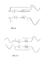
- the gyroscopic effect can be compensated in the control loop by a so-called “cross feedback”, in which the measured velocity in one direction is fed back to a torque in the other direction.
- the control loop comprises an inner loop that has a “cross feedback” term CFB, which acts on a measured rotor velocity in the ⁇ x and ⁇ y directions.
- the gain balancing matrix GB distributes the control forces over the actuators P, to create a decoupled system for the position controller C and the gain scheduling matrix GS.
- the gyroscopic effect is compensated not by feedback of a “cross feedback” term CFB but rather by a feedforward using so-called “gyroscopic compensation” GyC.
- a “gyroscopic compensation” GyC matrix is inserted between the gain scheduling matrix GS and the gain balancing matrix GB in the control loop.
- a highly accurate system may be achieved in which the gain balancing matrix GB distributes the control forces over the actuators P, in a feedforward decoupled system for the position controller C and the gain scheduling matrix GS.
- gyroscopic effects may be reduced or cancelled without determining or measuring the absolute velocity of the movable frame 8 .
- the GyC matrix is described in Equation 3 below:
- An exact GyC matrix as described above may in some circumstances lead to an unstable system. For example, instability may occur if ⁇ gyro , (depending on the inertias) is not known exactly. Accordingly, a “detuned” GyC may be used in the feedback path to help create a stable system.
- a high-pass filter may be included in the GyC compensation terms. The high-pass filter limits the gain of a pure integrator for low frequencies.
- a slightly lower GyC gain e.g. 0.99 instead of 1.00
- a disadvantage of tuning the GyC this way for stability is a decreased performance of the feedforward. To help alleviate this, referring to FIG. 12B , the control loop of FIG. 12A may be used with a detuned GyC (“GyC 1 ”) and added thereto may be an exact GyC (“GyC 2 ”) applied in the setpoint feedforward.
- reaction forces arising out of moving movable frame 8 should be reduced or eliminated.
- the reaction forces should not be permitted to act directly on the supporting frame 5 , 15 .
- a high controller bandwidth is used which can be severely disturbed by supporting frame dynamics in response to directly excited reaction forces. Accordingly, an isolation mechanism is desired.
- an isolation mechanism is meant a mechanism that completely isolates the supporting frame 5 , 15 from reaction forces or vibrations arising from moving the movable frame 8 (and/or completely isolates the movable frame 8 from vibrations or forces from the supporting frame 5 , 15 ) or at least significantly reduces/dampens such reaction forces or vibrations arising from moving the movable frame 8 (and/or at least significantly reduces/dampens vibrations or forces from the supporting frame 5 , 15 ).
- Such an isolation mechanism may comprise a reaction frame to which is connected the motor of the movable frame 8 in combination with a separate frame to which elements, that should be protected from the reaction forces or vibrations, are attached.
- the frames may be, for example, separately connected to ground or may be connected to each via a damper. Additionally or alternatively, one or more reaction masses (sometimes referred to as balance masses) may be used.
- a movable frame 8 system is shown schematically with one or more reaction masses 350 to absorb all or at least some of the reaction forces of the actuator 11 .
- a stationary part 5 e.g., a stiff rod
- This movable frame 8 system may include one or more of the motors 300 as described above and have an active magnetic bearing.
- This movable frame 8 system may also include one or more sensors 312 as described above.
- the stationary part 5 is stiffly connected to the frame 15 .
- the stationary part 5 is desirably stiffly connected to the frame 15 so that there is proper relation between the frame 15 , to which the substrate motion may be referenced, and the frame 8 .
- the stationary part 5 may be connected to frame 15 via an isolation mechanism 352 (e.g., a damper in the form of, for example, a spring or gas mount), which may require additional differential measurements to establish a proper relation between the frame 8 and frame 15 (and/or other structures).
- the frame 15 may be connected to the ground via an isolation mechanism 354 (e.g., a damper in the form of, for example, a spring or gas mount), which may require additional differential measurements.
- the reaction mass 350 is movably connected to the stationary part 5 .
- the reaction mass 350 may be connected to the stationary part 5 by, for example, a spring. Connected to the reaction mass is a part of the motor 300 , while another part of the motor 300 is part of or connected to the frame 8 .
- reaction forces are absorbed by the reaction mass 350 such that all, or at least a significant amount, of the reaction forces do not transmit into the stationary part 5 .
- FIG. 13B depicts a schematic side view of an embodiment of the portion outlined by dashed box of FIG. 13A
- FIG. 13C depicts a schematic top view of an embodiment of the portion outlined by dashed box of FIG. 13A
- a coil (electromagnet) part of the motor 300 is mounted in or on the reaction mass 350 . While 4 coil parts of the motor 300 are shown, another number of coil parts may be provided.
- the coil part of the motor 300 interacts with the frame 8 to cause the frame to move.
- the frame 8 may be made of steel such that the interaction of the coil part of the motor 300 with the frame 8 causes the frame 8 to move.
- a specific structure may be mounted in or on the frame that is the part of the motor 300 that cooperates with the coil part of the motor 300 .
- coil part of the motor 300 may be on the frame 8 and the other part of the motor 300 on the reaction mass 350 .
- the reaction mass 350 may be a single monolithic structure (e.g., a cylinder that surrounds the stationary part 5 ) to which the one or more coil parts of the motor 300 are attached. In an embodiment, there may be one or more reaction masses 350 , for example there may be 2, 3, 4 or more separate reaction masses. More than one coil part of the motor 300 may be mounted per reaction mass. In an embodiment, each coil part of the motor 300 has its own reaction mass 350 .
- one or more of the reaction masses 350 may move in up to and including 6 degrees of freedom. In an embodiment, one or more of the reaction masses 350 may move in only 1, 2, 3 or 4 degrees of freedom.
- one or more sensors 312 are mounted on the stationary part 5 to measure the position of the movable frame 8 directly with respect to the stationary part 5 .
- Each sensor 312 may measure in a single direction (e.g., Y-direction, X-direction, etc) or measure in multiple directions (e.g., X and Y directions).
- a gap may be provided internally to the reaction mass 350 to allow sensor 312 to measure the movable frame 8 .
- a gap may be provided between a plurality of reaction masses 350 to allow sensor 312 to measure the movable frame 8 .
- At least two motors 300 may be provided—one at each opposite side of the rotor (see also, e.g., the upper set of motors 300 in FIG. 7 , the lower set of motors 300 in FIG. 7 , the upper set of motors 300 in FIG. 13B or the lower set of motors 300 in FIG. 13B ).
- a reason for this is that the particular motor may exert a unidirectional force.
- the at least two motors 300 for a particular actuation direction are connected to a same reaction mass 350 . This arrangement allows a higher mass of the total reaction mass, limiting its excursions.
- FIG. 13D a variation of the embodiment depicted in FIG. 13B is shown.
- a part of the motor 300 is mounted in or on the reaction mass 350 .
- the 2 depicted upper parts of the motor 300 cause movement of the frame 8 in the X-direction while 2 further upper parts of the motor 300 (not shown but at 90 degrees to the two depicted upper parts of the motor 300 ) cause movement of the frame 8 in the Y-direction.
- the 2 depicted lower parts of the motor 300 cause movement of the frame 8 in the Z-direction.
- a further lower part of the motor 300 may be provided to cause movement in the Z-direction.
- the motor 300 can actuate in the Z, Rx and Ry directions.
- the parts of the motor 300 may cause the frame to rotate around the Z-axis.
- each or all of the parts of the motor 300 may be parts of a reluctance motor.
- one or more sensors 312 are mounted on the stationary part 5 to measure the position of the movable frame 8 directly with respect to the stationary part 5 . In this case, the sensor 312 is mounted outside of the periphery of the reaction mass 350 in order to measure the frame 8 .
- reaction masses 350 By using one or more reaction masses 350 , a stable system at the desired bandwidth may be obtained. Reaction forces can be filtered before entering the stationary part 5 , enabling high servo control bandwidth and small position error.
- the system may have a reaction mass 350 of 1 kg at 20 Hz, a stationary part 5 of 10 kg at 500 Hz, a movable frame 8 of 80 kg, a frame 15 of 5000 kg at 150 Hz and a gas mount 354 for 1.5-3 Hz.
- a stable system with low or no reaction forces in the stationary part 5 may be achieved.
- FIG. 15 a Bode plot of simulated data shows, for example, the mechanical transfers in the X-direction without a reaction mass.
- a Bode plot of simulated data shows the mechanical transfers in the X-direction with a reaction mass.
- the reaction path With the reaction mass, the reaction path remains away from the action path above 200 Hz. Further, it can be seen from FIG. 16 that the reaction mass may not address frequencies below 20 Hz, because this range of frequencies shouldn't affect stability due to the lack of resonances.
- the reaction path is amplified at about 20 Hz, i.e., the reaction forces are amplified, however this is lower than the bandwidth of the control system and so does not have a significant deleterious effect. Frequencies about or less than 20 Hz can be addressed, if needed, in another manner (e.g., damping). As for frequencies above about 20 Hz, the reaction mass is effective at keeping the reaction path away from the action path.
- the forces may sometimes be too large to be absorbed by the reaction mass; the excursion of the reaction mass may become too large.
- This may be the case, for example, (1) when tracking a 6-degrees of freedom profile by the movable frame 8 (e.g., maintaining the movable frame 8 's appropriate position and orientation with the respect to the substrate, e.g., leveling) and/or (2) when large repeating disturbances need to be compensated, e.g. characteristics from a gravity compensator acting in the Z direction to position the movable frame 8 along the Z-axis).
- a possible solution is to use at least two motors 356 , 358 in place of where one motor 300 would be used.
- the first motor 356 connected to the reaction mass 350 , only applies servo feedback forces 360 .
- the second motor 358 connected directly to the stationary part 5 , only applies servo feedforward forces 362 .
- the servo feedforward forces are much higher, but do not need to be isolated by a reaction mass since they cannot destabilize the control loop.
- a bias current can be used on the corresponding opposing motor. An actuated force then is translated into a larger current in one motor, and a smaller current in another motor. This may mean no need to switch amplifiers from one motor to the next.
- the movable frame 8 may suffer from internal dynamics that interferes with obtaining high controller bandwidth. Accordingly, it is desirable to obtain higher bandwidth, which can lead to better accuracy and better accuracy. The following measures can help to achieve such higher bandwidth, better accuracy, and/or better imaging.
- FIG. 18 depicts a schematic top view of a movable frame with a plurality of motors 300 (e.g., 4 motors such as reluctance motors) evenly spaced around a part of the frame 4 .
- motors 300 are located at the 0°, 90°, 180° and 270° positions.
- FIG. 18 also depicts a plurality of sensors 312 (e.g., 3 sensors) to measure a position/force of the movable frame 8 in the X, Y directions. The sensors are evenly spaced around a part of the frame 4 .
- the sensors 312 are located at the 45°, 165°, and 285° positions.
- the frame 8 of FIG. 18 is shown being rotated.
- the movable frame 8 may adopt, as one of its modes, an ellipsoidal shape at a certain frequency as shown in FIG. 19 .
- This shape is picked up by the sensors 312 and actuated by the motors 300 , and will hence show up in the mechanical system that the controller tries to control.
- Such a mode and/or other low modes become “visible” in the control loop and thus made lead to reduced bandwidth.
- a low bandwidth may result in larger positioning errors, and in the case of a rotatable frame 8 may lead to instability at a high rotation speed.
- a sensor is located at an angular position that substantially bisects the angular positions of two adjacent motors. For example, if adjacent motors are located at the 0° and 90° positions respectively, the sensor is located at about the 45° position. So, referring to FIG. 20 , in an embodiment, the motors 300 are located at the 0°, 90°, 180° and 270° positions such as shown in FIGS. 18 and 19 .
- FIGS. 21(A) -(D) show some mode shapes of frame 8 that are actuated by one or more of the motors 300 , but not observed as an ellipsoid by the sensors 312 .
- a Bode plot depicts simulated results using a dynamic model of a rotor with and without the motor 300 /sensor 312 orientation of FIG. 20 .
- Curve 400 shows the normal response without the motor 300 /sensor 312 orientation of FIG. 20 .
- Curve 402 shows the response with the motor 300 /sensor 312 orientation of FIG. 20 , wherein sensors 312 are radial sensors.
- Curve 404 shows the response with the motor 300 /sensor 312 orientation of FIG. 20 , wherein sensors 312 are tangential sensors. It can be seen, for example, that the about 830 Hz mode in curve 400 is no longer apparent in curves 402 and 404 .
- eight motors 300 are used to obtain X and Y displacements, and Rx and Ry rotations.
- a first set of four motors 300 (shown as dashed line squares) is at or close to the top of the movable frame 8
- a further set of four motors 300 (shown as solid line squares) are at or close to the bottom of the movable frame 8 .
- each motor of the bottom set of motors 300 (shown as dashed line squares) is located at an angular position that substantially bisects the angular positions of two adjacent motors of the top set of motors 300 (shown as solid line squares). For example, referring to FIG. 24 , if adjacent motors 300 of the top set of motors 300 are located at the 0° and 90° positions respectively, a motor of the bottom set of motors 300 is located at about the 45° position.
- the bottom set of motors 300 is rotated about 45 degrees with respect to the top set of motors 300 .
- a X, Y, Rx or Ry force is applied, only the top set of motors 300 or the bottom set of motors 300 may excite the mode, but not both at the same time.
- the movable frame 8 may suffer from bandwidth limiting internal dynamics.
- movable frame 8 may adopt, as one of its modes, an ellipsoidal shape at a certain frequency. This shape can be picked up by the sensors 312 shown in FIG. 19 and actuated by the motors 300 , and will hence show up in the mechanical system that the controller tries to control.
- Such a mode and/or other low modes become “visible” in the control loop and thus may lead to reduced bandwidth.
- a low bandwidth may result in larger positioning errors, and in the case of a rotatable frame 8 may lead to instability at a high rotation speed.
- a solution is to have certain (i.e. low frequency) mode shapes be unobserved and/or not be actuated as those mode shapes.
- a plurality of individual sensor signals are combined to generate unobservability, e.g., by means of averaging. For instance, as discussed above with respect to FIG. 21 , averaging can make a mode shape “unobservable” and/or not be actuated as that mode shape when sensors are placed opposite of one another (i.e., at 180 degrees with respect to each other relative to a center of the frame) and the mode shape is also opposite on those positions, and thus the sensors measure a 180 degrees phase shifted error signal. For example, as depicted in FIG.
- an ellipse mode shape with arbitrary rotation can become “unobservable” using a first set of two sensors opposite each other along a first direction and a second set of two sensors opposite each other along a second direction, the second direction of the second set being substantially perpendicular to the first direction of the first set.
- more than two sets of sensors may be employed to measure the position of the frame and facilitate making a mode shape of the frame “unobservable” and/or not be actuated as that mode shape.
- Those additional sets of sensors may be used to make the measurement more accurate and/or to make the frame more “unobservable” and/or less actuated as that mode shape.
- the additional sets may be used to make a mode shape of the frame “unobservable” and/or not be actuated as that mode shape where two sets may not be able to, for example, if the mode shape is not an ellipse or not a uniform ellipse.
- a set of sensors may comprise more than two sensors. More than two sensors in a set may be used, for example, to measure an irregular ellipse mode shape (e.g., an ellipse type shape that is not uniformly elliptical).
- tangential metrology is used to measure in a direction substantially perpendicular to a direction of mode shape manifestation, which facilitates making the mode shape to be unobserved and/or not be actuated as the mode shape. This is because measurement in a tangential direction is (rather) insensitive to the mode shape, which manifests itself mainly in a radial direction (e.g. an ellipsoidal mode shape).
- tangential metrology is meant measurement at a tangent to a surface of the frame and/or to a radius from the axis of rotation.
- a surface of the frame 8 used for measurement with tangential metrology need not be a curved (e.g., circular arc) surface nor need it be an outer surface of frame 8 .
- one or more tangential sensors 380 are provided to measure the frame 8 in a substantially tangential direction.
- five tangential sensors 380 are provided to allow for five degrees of freedom (X, Y, Rx, Ry, and Rz) measurement and thus control of positioning in the five degrees of freedom.
- three tangential sensors 380 are evenly spaced around the rotation axis of the frame 8 at the top half of the frame 8 .
- a further two tangential sensors 380 are spaced around the rotation axis of the frame 8 at the bottom half of the frame 8 .
- the three tangential sensors 380 may be at the bottom half of the frame 8 and the two tangential sensors 380 may be at the top half of the frame 8 .
- An additional sensor 382 is provided for axial (Z-direction) measurement and thus control of positioning in the axial direction.
- one or more of the sensors 380 , 382 may be an encoder system.
- the scale of the encoder system is in or on the frame 8 and the sensor, transducer or readhead of the encoder system is on the stationary part 5 and/or frame 15 .
- the scale of the encoder system is in or on the stationary part 5 and/or frame 15 and the sensor, transducer or readhead of the encoder system is on the frame 8 .
- one or more of the sensors 380 , 382 may be a capacitive sensor, an Eddy current sensor, or a confocal sensor.
- each of the sensors 380 is an encoder system and sensor 382 is a capacitive sensor, an Eddy current sensor, or a confocal sensor.
- each tangential sensor 380 comprises a sensor, transducer or readhead 384 in combination with a scale 386 .
- the scale 386 is attached to the frame 8 .
- FIG. 26(A) Depicted in FIG. 26(A) are two of the tangential sensors 380 associated with the top half of the frame 8 and depicted in FIG. 26(B) are depicted the three tangential sensors 380 associated with the top half of the frame 8 .
- the scale 386 is attached to a lateral outer surface of the frame 8 with the sensors, transducers or readheads 384 arranged with their sensing surfaces facing, in the direction shown by the respective arrows, at the scale 386 ; as will be appreciated, the scale 386 could on or in another surface of frame 8 .
- the scale 386 is shown as being continuous, it need not be.
- the scale 386 may be segmented around the outer lateral surface of frame 8 into subscales 386 that are, for example, each associated with a particular sensor, transducer or readhead 384 .
- the scale 386 comprises a linear grating.
- the movement in the X and/or Y directions of frame 8 can be determined as well as rotation around the Z-axis.
- movement around the X and/or Y directions of frame 8 can be determined.
- each tangential sensor 380 comprises a sensor, transducer or readhead 384 in combination with a scale 386 .
- the scale 386 is attached to the frame 8 .
- FIG. 27(A) Depicted in FIG. 27(A) are two of the tangential sensors 380 associated with the top half of the frame 8 and depicted in FIG. 27(B) are depicted the three tangential sensors 380 associated with the top half of the frame 8 .
- the scale 386 is attached to an outer top (or bottom) surface of the frame 8 with the sensors, transducers or readheads 384 arranged with their sensing surfaces facing, in the direction shown by the respective arrows, at the scale 386 .
- the scale 386 is shown as being continuous, it need not be.
- the scale 386 may be segmented around the outer top (or bottom) surface of frame 8 into subscales 386 that are, for example, each associated with a particular sensor, transducer or readhead 384 .
- the scale 386 comprises a linear grating.
- the movement in the X and/or Y directions of frame 8 can be determined as well as rotation around the Z-axis.
- movement around the X and/or Y directions of frame 8 can be determined.
- FIGS. 26 and 27 A combination of the arrangements depicted in FIGS. 26 and 27 may be employed.
- the arrangement of one or more tangential sensors 380 shown in FIG. 26 may be used for the top half of a frame 8
- the arrangement of one or more tangential sensors 380 shown in FIG. 27 may be used for the bottom half of the frame 8 , or vice versa.
- Other combinations will be apparent to those skilled in the art.
- An advantage of a tangential sensor is its relative insensitivity for radial variation (e.g. in view of range dissipation) resulting from and dependent on angular velocity.
- the variations may be in the order of 100 microns.
- Insensitivity to radial variation expansion or contraction
- a mode shape manifesting itself in a radial direction is essentially unobservable using a tangential sensor, allowing for a higher bandwidth, and as such improved position- and imaging accuracy.
- a tangential sensor can have an advantage over a sensor measuring in the radial direction in that the radial sensor will likely have a curved measurement surface, thus limiting accuracy.
- an advantage of an encoder system in this application is its stand-off distance (i.e., the distance between encoder head and scale).
- the relatively large stand-off distance of an encoder system can increase robustness for (i) emergency stops (e.g., frame 8 crash) and/or (ii) assembly/serviceability.
- the stand-off distance for an encoder system for high resolution measurement e.g., 10 nm resolution
- the stand-off distance for an encoder system for high resolution measurement can be in the order of millimeters (even up to 10 mm) compared to a nominal stand-off distance for, e.g., a capacitive sensor of approximately 10 5 ⁇ resolution, which translates to a stand-off distance of about 0.1 mm when the resolution is about 10 nm.
- an optical sensor such as an encoder system, will not be influenced by magnetic fields generated by, for example, actuators.
- An advantage, in addition to or alternatively from insensitivity to radial variation, is that the number of sensors may be reduced compared to, e.g., a system that measures radially. Reduction in the number of sensors can (i) reduce noise (and increase accuracy), and/or (ii) reduce cost and yield. However, it is not necessary that the number of sensors be reduced and indeed having a greater number of sensors (at the sake of, for example, cost) may mean less noise if averaging of the sensor is employed. Noise reduces with the inverse square root of the number of sensors used and so more sensors means less noise in the total result.
- a movable frame 8 is desirably balanced to reduce or minimize unbalance in the frame 8 (e.g., balanced by strategically adding weight or removing weight similar to balancing of a vehicle tire); the frame 8 should be very well mechanically balanced.
- each frame 8 may be balanced to, e.g., 2 kg* ⁇ m.
- a frame 8 has an imbalance of some amount (even if very small) resulting in application of a net force to the frame 5 , 15 by the frame 8 .
- the net force applied by each frame 8 is symbolically depicted by the vector 410 associated with the frame 8 .
- the vector is merely exemplary of the net direction and magnitude of the force; the vector may be of different direction and/or magnitude and the actual force may be time-varying in direction and magnitude due to the movement of the frame 8 .
- vector 410 represents the direction and magnitude of the force exchanged between the frame 8 and the frame 5 , 15 .
- the force 410 arises, e.g., due to the axis offset of the axis of the frame 8 relative to the frame 5 , 15 , the direction and magnitude of the axis offset shown by vector 420 . Additionally or alternatively, the force 410 arises, e.g., due to the center-of-gravity offset of the frame 8 relative to the center (e.g., the imaging or optical center) of the frame 8 , the direction and magnitude of the center-of-gravity offset shown by vector 430 .
- Other potential causes of the imbalance can include the environment of the frame 8 affecting the frame 8 , e.g., gas (if any), and optionally a gas flow, in the environment, a magnetic, electrostatic and/or electric force in the environment (e.g., from another frame 8 , from an actuator to move the frame 8 , etc.), a bearing associated with the frame 8 (e.g., a magnetic and/or gas bearing), etc.
- gas if any
- a gas flow in the environment
- a magnetic, electrostatic and/or electric force in the environment e.g., from another frame 8 , from an actuator to move the frame 8 , etc.
- a bearing associated with the frame 8 e.g., a magnetic and/or gas bearing
- the imbalanced frame 8 may have a deleterious effect on the supporting frame 5 , 15 , on another frame 8 , and/or on one or more other components in the apparatus 1 .
- the frame 8 's imbalance on its own, or in combination with the imbalance of one or more other frames 8 may be sufficient to cause deleterious effects on the supporting frame 5 , 15 , on another frame 8 , and/or on one or more other components in the apparatus 1 .
- the combined effect of a plurality of slightly imbalanced frames 8 on a common frame 5 , 15 may be sufficient to cause deleterious effects on the supporting frame 5 , 15 , on one or more of the frames 8 , and/or on one or more other components in the apparatus 1 , when the individual imbalances themselves may not have caused a deleterious effect.
- frame 8 imbalance it is desirable to remedy frame 8 imbalance to within tight imaging specifications and/or reduce or eliminate dynamical vibration interaction between frames 8 , between frame 8 and supporting frame 5 , 15 , and/or between any number of other components as a result of frame 8 imbalance.
- the position (e.g., rotation) of one or more of the frames 8 can be tuned to reduce or cancel a total imbalance effect on, for example, support frame 5 , 15 due to the frames 8 .
- an angular position (rotation angle) of one or more of the frames 8 relative to the one or more other frames 8 can be chosen such that a total force on the frame due to imbalance of one or more of the frames 8 is reduced or minimized.
- a frame 5 , 15 may support a plurality of movable frames 8 .
- each frame 8 generally rotates about an axis 10 of the respective frame 8 .
- Each frame 8 includes a plurality of lenses 14 , 18 (only 1 lens 14 , 18 is shown in one frame 8 for clarity although it should be appreciated there may be a plurality of lenses 14 , 18 for each frame 8 as shown, for example, in FIGS. 3 and 6 ).
- each frame 8 has an imbalance of some amount (even if very small) resulting in application of a net force to the frame 5 , 15 by the frame 8 .
- the net force applied by each frame 8 is symbolically depicted by the respective vectors 410 associated with the frames 8 .
- the vectors are merely exemplary of the net direction and magnitude of the forces; the vectors may be of different directions and/or magnitudes and the actual forces may be time-varying in direction and magnitude due to the movement of the frame 8 .
- the sum of all the net forces of the frames 8 caused by their respective imbalances (if any) would yield a zero net force on the frame 5 , 15 .
- there should be no or little deleterious effect on the supporting frame 5 , 15 to due the imbalance there should be no or little deleterious effect on another frame 8 since the frame 5 , 15 , via which the imbalance force would be transmitted, has substantially no net force due to the imbalance, and there should be no or little deleterious effect on one or more other components in the apparatus 1 since the frame 5 , 15 , via which the imbalance force would be transmitted, has substantially no net force due to the imbalance.
- the magnitude and direction of the imbalance of each of the frames 8 is measured separately.
- the imbalance of the frame 8 may be measured in various ways and at various times. For example, the imbalance may be measured during use of the frame 8 (e.g., to reduce downtime of the apparatus) and/or may be measured when a frame 8 is not being used (e.g., during a (re-)calibration or maintenance procedure). Further, the frame 8 may be measured in place on the frame 5 , 15 and/or measured when removed from the frame 8 (e.g., removed from the frame 5 , 15 and measured in a separate imbalance measurement tool).
- a non-limiting example of how the imbalance can be measured is to obtain a measurement signal (e.g., a signal from a force sensor or accelerometer attached to, e.g., frame 5 , 15 ) of one of the frames when it is disturbed in a horizontal direction (e.g., in the X- and/or Y-direction) at a frequency different than its rotating frequency (e.g. 78 Hz or 80 Hz) and compare that with a measurement signal at its rotating frequency, such that a beat frequency is produced which indicates the ‘position’ of the unbalance in angular units (e.g. degrees).
- a measurement signal e.g., a signal from a force sensor or accelerometer attached to, e.g., frame 5 , 15
- a frequency different than its rotating frequency e.g. 78 Hz or 80 Hz
- FIG. 30(A) shows the two measurement signals (E 1 and E 2 ) having different frequencies—one at the normal rotation frequency and the other at the different frequency—shown here as a function of their angular position with respect to time.
- FIG. 30(B) shows the superposition of those two signals E 1 and E 2 .
- FIG. 30(C) shows the sine, which can be discriminated when analyzing FIG. 30(B) .
- FIG. 30(D) shows the beat frequency as a function of the two other frequencies (note that the minimum amplitude does not need to return to zero in FIG. 30(D) , but may have an offset, since the input frequencies will probably have different amplitudes).
- This beat frequency is a measure for the unbalance, which changes amplitude in time, however at a frequency much smaller than the rotational, or disturbing, frequency.
- This amplitude variation is a function of phase difference between the two input frequencies, hence the tangential position of the unbalance can be determined.
- the unbalance of the frame can be counteracted at frequency with a correction (e.g., application of a single or plurality of known forces) and if the measurement yields no or little imbalance, the amplitude can be determined.
- a correction e.g., application of a single or plurality of known forces
- the measurements yields no or little imbalance the amplitude can be determined.
- both angular position and magnitude of the unbalance can be determined.
- the measurements and calculations may be performed for a range of frequencies to improve the accuracy (and to exclude frequencies of, e.g., one or more other frames).
- the imbalance of a frame 8 can be measured indirectly by measuring the position, vibration of and/or force applied to the frame 5 , 15 .
- radiation projected through the lenses 14 , 18 of a frame may be measured by a radiation sensor (e.g., an intensity sensor) to determine variation of the radiation which correlates to the imbalance.
- the sensor may measure the spots projected by a frame 8 to determine the imbalance.
- a radiation sensor e.g., an intensity sensor
- the sensor may measure the spots projected by a frame 8 to determine the imbalance.
- a sensor could be, for example, a transmission image sensor.
- the sensor could be located, for example, on the table 2 .
- a beam splitter may be in, or inserted into, the path of the beam in order to allow the beam to be sampled for measurement by a sensor.
- servo position error of the frame 8 e.g., of the frame 8 with respect to the frame 5 , 15
- a measurement beam may be used to measure the position of the frame 8 relative to, e.g., frame 5 , 15 and/or a frame on which the detector is mounted.
- Appropriate intermediate measurements may be made to put the measurements of frame 8 into the appropriate coordinate system, e.g., a measurement between a frame holding the sensor and the frame 5 , 15 , etc.
- the imbalance of a frame 8 can be measured in various different ways using various different systems and/or tools. Moreover, it may not be necessary to obtain values for the angular position and the magnitude of the imbalance. For example, it may be sufficient just to have an indication of the direction of the imbalance if, for example, the magnitude of the imbalance of each frame 8 is substantially, or closely enough, the same.
- the imbalance may be corrected at various times. For example, the imbalance may be corrected during use of the frames 8 (e.g., as the frames are being used to project radiation, during a time between exposure of different target portions, during a time between exposure of different substrates, etc.) and/or may be corrected when the frames 8 are not being used (e.g., during a (re-)calibration or maintenance procedure). Further, an imbalance may be corrected for a particular frame 8 or may be corrected in aggregate for a plurality of frames 8 .
- the correction for a particular frame 8 of the plurality of frames 8 may different than if an imbalance of the frame 8 were corrected just to reduce or eliminate the imbalance for the frame 8 .
- an imbalance of a frame 8 may not be reduced in of itself but rather re-oriented such that it can cancel out an imbalance of another frame 8 .
- the imbalance may be corrected by adjusting the position of one or more frames 8 relative to one or more of the other frames 8 .
- such correction should take account the position of the one or more other frames 8 .
- the adjustment of the one or more frames 8 should be such that the forces that each frame 8 puts on the frame 5 , 15 cancels as much as possible the forces being put on the frame 5 , 15 by the other one or more frames 8 .
- the adjustment of the position comprises adjusting the angular position of one or more frames 8 relative to the angular position of one or more other frames 8 . More specifically, the angular position of a particular portion of a frame 8 at a certain time in its rotation is adjusted relative to the angular position of a particular portion of another frame 8 at that same time.
- FIG. 31 the frame 5 , 15 supporting the plurality of movable frames 8 of FIG. 29 is shown.
- the frames 8 rotate about their respective axis 10 .
- FIGS. 29 and 31 show, for example, the frames 8 during their respective rotations at a particular point in time.
- FIG. 31 has its angular position adjusted relative to the other frames as can be seen when compared with FIG. 29 .
- the depicted lens 14 , 18 e.g., lens 1 of X number of lenses
- the phase angle of the frame 8 is adjusted even though it rotates at the same frequency.
- the direction of the imbalance is changed (and optionally the magnitude may be changed depending on the nature of the imbalance of that frame 8 ).
- the location of a lens 14 , 18 relative the radiation beam from controllable element 4 is significant.
- the lens 14 , 18 may need to be in a particular position with respect to that beam so that it can appropriately receive the beam.
- a lens 14 , 18 of another frame 8 receiving a radiation beam may also need to be in a particular position when receiving its beam and also in a particular position with respect to the lens 14 , 18 of another frame.
- the lenses 14 , 18 of different frames 18 may need to be in aligned in a particular orientation to expose a target portion.
- the change in position of the frame 8 to compensate at least in part for imbalance may take into account the position of the one or more lenses 14 , 18 on the frame 8 .
- a frame has a plurality of lenses 14 , 18 around the center axis 10 (see, e.g., FIGS. 3 and 6 although FIGS. 29 and 31 show just one lens 14 , 18 for clarity purposes).
- the number of angular position adjustments available for a frame 8 includes at least the number of lens 14 , 18 around the axis 10 . For example, if 200 lenses 14 or 18 are arranged around the axis 10 of a particular frame 8 , then 200 angular positions of the frame 8 are possible without having to adjust illumination timing.
- a large number of lenses on the frame 8 allows for a significant adjustment freedom, and thus for a significant reduction of excitation force.
- a six degrees of freedom imbalance effect in all directions can be taken into account, given ten movable frames 8 with ten imbalance vectors.
- the illumination adjustment may be used to help effect position adjustment, e.g., to an angle in between two adjacent lenses 14 , 18 around the axis 10 .
- the frame 8 can be adjusted to a particular position and if the lens 14 , 18 is not appropriately aligned with respect to a beam, e.g., in the case where the beams all are synchronously provided to each of the frames 8 from the controllable elements 4 , the timing of the projection of radiation onto a lens 14 , 18 of a frame 8 may be adjusted vis a vis the projection of radiation onto a lens 14 , 18 of another frame, e.g., the beams become asynchronous or differently asynchronous. If needed, appropriate shifting of the projection of a portion of the pattern may need to be shifted or shared between frames 8 through the apparatus controller adjusting the allocation of the pattern production among the frames 8 .
- an additional or alternative way the imbalance for one frame 8 or for a plurality of frames 8 may be corrected is to adjust the imbalance of a particular frame 8 itself.
- the frame 8 may have weight added or removed to change the direction and/or magnitude of the imbalance.
- an additional or alternative way the imbalance may be corrected for one frame 8 or for a plurality of frames 8 is to adjust the frame 5 , 15 supporting the one or more frames 8 .
- an actuator may be used to apply a counterbalancing force to the frame 8 to compensate at least in part for the force applied to the frame 5 , by the one or more frames 8 .
- the net imbalance imparted by all the frames 8 supported on the frame 5 , 15 may be determined (by calculation and/or by measurement) and a counterbalancing force may be applied to the frame 5 , 15 by the actuator.
- Such application of force may be complex due the movement of the frames 8 and the actuator will need to operate at the substantially same frequency as the frames 8 .
- An additional or alternative way the imbalance may be corrected for one frame 8 or for a plurality of frames 8 is to employ a balance or reaction mass for the one or more frames 8 or a balance or reaction mass for the frame 5 , 15 supporting the one or more frames 8 .
- a balance or reaction mass for the one or more frames 8 or a balance or reaction mass for the frame 5 , 15 supporting the one or more frames 8 .
- the balance or reaction mass may be configured to cancel out in part or as a whole forces in a particular one direction, in two directions (e.g., X-Y plane), in three directions, in four directions (e.g., X-Y-Z and rotation about 1 of the three directions), in five directions or in six directions.
- An additional or alternative way the imbalance may be corrected for one frame 8 or for a plurality of frames 8 is to employ a correction of the data used to control one or more controllable elements 4 (and/or one or more other modulating devices) to compensate at least in part for the imbalance of the one or more frames 8 .
- hardware and/or software constituting a “data-path” may be provided to convert a vector-based representation of a desired device pattern to be formed on a substrate to a control signal suitable for driving a programmable patterning device.
- FIG. 32 is a schematic illustration showing example processing stages 100 that may be included in such a data-path. In an embodiment each of the stages is connected directly to its neighboring stages. However, this need not be the case. In an embodiment one or more additional processing stages may be provided in between any of the stages shown. Additionally or alternative, each of one or more of the stages may comprise multiple stages. One or more of the stages may be combined.
- a vector-based representation of a desired device pattern is provided in stage 102 .
- the vector-based representation may be constructed using a vector design package such as GDSII.
- the stored vector-based representation is forwarded to a rasterization stage 104 , either directly or via one or more intermediate stages. Examples of intermediate stages include a vector pre-processing stage and a low-pass filter stage.
- the low-pass filter stage may perform anti-aliasing processing for example.
- the rasterization stage 104 converts the vector-based representation (or a processed version of the vector-based representation) of the desired device pattern to a rasterized representation of a desired dose pattern that corresponds to the desired device pattern (i.e. is suitable for forming the desired device pattern by post-exposure processing of the substrate).
- the rasterized representation may comprise bitmap data, for example.
- the bitmap data may be referred to as “pixelmap” data.
- the bitmap data may comprise a set of values indicating the desired dose at each point on a grid of points.
- the grid of points may be referred to as a rasterization grid.
- the rasterized representation (as output from the rasterization stage 104 directly or after further processing) may be supplied to a control signal generation stage 106 .
- the control signal generation stage 106 may be implemented as a single stage (as shown) or as a plurality of separate stages.
- the control signal generation stage 106 may perform a mapping operation between the rasterization grid and the grid (which may be referred to as the “spot exposure grid”) defining the locations at which the patterning device can form spot exposures at the target (e.g., substrate) level.
- the mapping operation may comprise interpolation between the rasterization grid and the spot exposure grid.
- the mapping operation may be configured to receive metrology data from a metrology data storage stage 108 .
- the metrology data may specify, for example, the position and/or orientation of the mounted substrate, and/or a previously formed device pattern on the mounted substrate, relative to the patterning device.
- the metrology data may also specify measured distortions of a mounted substrate or previously formed device pattern.
- the distortions may include shift, rotation, skew and/or magnification, for example.
- the metrology data therefore provides information about how the interpolation between the rasterization grid and the spot exposure grid should be carried out in order to ensure proper positioning of the desired dose pattern on the target.
- the metrology data may also include information about the imbalance of one or more frames 8 .
- the control signal generation stage 106 may calculate a set of intensities to be applied at each position in the spot exposure grid to form the desired dose pattern.
- the set of intensities may define, for each position in the grid, the intensity of the radiation beam that is to be used to generate the spot at that position, for example. This calculation may account for the properties of the optical projection system and may therefore be referred to as an “inverse-optics” calculation.
- the calculation may account for the sizes and/or shapes of individual spots, for example, which may be dictated by properties of the optical projection system.
- the size and/or shape may be defined for each of a given set of possible applied intensities for the spot.
- the spot size and/or shape may define the variation with position of the applied dose for a given spot for example.
- the calculation may also take into account deviations in the positions of the spots from nominal positions defined by the ideal (i.e. engineering error free) spot exposure grid geometry.
- the spots may overlap with each other at target level so that the final dose achieved at a reference position in the spot exposure grid may depend on the applied intensities at a number of neighboring spots.
- This effect may be modeled mathematically by a convolution operation.
- the control signal generation stage 106 needs to perform the reverse process (determine the intensities that need to be applied at each position for a given desired dose pattern), so a deconvolution operation may be performed.
- the deconvolution operation may be defined by a deconvolution kernel.
- the deconvolution kernel may be represented by a deconvolution matrix.
- the coefficients of such a deconvolution matrix may be interpreted as weights that define the extent to which the dose at points in the region of a reference point in the desired dose pattern need to be taken into account when calculating the intensity to be applied at the corresponding point (or spot) in the spot exposure grid.
- FIGS. 33 and 34 illustrate schematically a step in such a deconvolution operation.
- FIG. 33 illustrates a portion of an example spot exposure grid 120 .
- Each point 125 in the grid 120 represents the center of a spot that will be formed by the patterning device on the target.
- the deconvolution operation aims to determine the intensity value to apply at each of the points 125 .
- the spot exposure grid 120 will have a geometry that corresponds to the pattern of spot exposures that the patterning device is able to form on the target.
- the geometry of the spot exposure grid may therefore be irregular.
- the density of grid points varies as a function of position so that it is not possible to construct the grid completely by tessellating a single unit cell that contains a single grid point only.
- the geometry of the grid 120 that is illustrated in FIG. 33 is greatly simplified and does not necessarily resemble a spot exposure grid associated with a commercial device.
- FIG. 34 illustrates an example portion of a rasterization grid 122 .
- the rasterization grid 122 has a regular geometry.
- the regular geometry is rectangular.
- the density of grid points of a regular grid within the meaning of the present application, is “uniform” in the sense that the grid can be completely formed by tessellating a single type of unit cell that comprises a single grid point only.
- Dotted line 121 illustrates an example unit cell. The dotted line intersects a quarter of four grid points and therefore contains one grid point in total.
- a sample of the desired dose pattern may be provided at each of the points 126 in the grid 122 .
- the solid grid point 123 in FIG. 33 represents a reference grid point (chosen at random).
- Application of the deconvolution operation for deriving the intensity to be applied at the solid grid point 123 will involve weighted contributions of the samples of the desired dose pattern at a plurality of grid points in the spot exposure grid in the region of the spot exposure grid corresponding to the position of the reference grid point 123 .
- the solid grid points 127 in FIG. 34 represent schematically the grid points that may be involved with such a deconvolution operation.
- a deconvolution kernel expressed as a matrix will define which grid points 126 are involved (by the positions of the non-zero coefficients in the matrix) and the extent to which the grid points are involved (by the values of the non-zero coefficients in the matrix).
- the nature of the deconvolution operation may be different for different points in the spot exposure grid and/or between points. This variation may take into account variations in the optical performance of the patterning device for example.
- the variations in optical performance may be obtained using calibration measurements.
- a library of deconvolution kernels, optionally obtained from calibration measurements, may be stored and accessed as needed.
- the control signal generation stage 106 may convert the sequence of intensity values to be applied at each of the points in the spot exposure grid to setpoint values in order to generate the control signal.
- the setpoint values may take into account the nature of the patterning device. For example, where the patterning device comprises a plurality of self-emissive contrast devices, the setpoint values may account for non-linearity in the response of the self-emissive contrast devices. The setpoint values may take into account variations in the properties of nominally identical contrast devices by calibration measurements for example.
- a control signal output stage 110 receives the control signal from the control signal generation stage and supplies the signal to the patterning device.
- stages 102 and 104 are performed in an offline part 112 of the data-path and stages 106 - 110 are performed in an online part 114 of the data-path.
- all or a portion of the functionality associated with stage 104 could be carried out online.
- all or a portion of the functionality of stages 106 and/or 108 could be carried out offline.
- the data may be mathematically manipulated using, for example, control signal generation stage 106 to cause a compensating shift of at least part of the pattern in the X-Y plane. Since the imbalance of the frame 8 can cause a displacement or vibration of the lens 14 , 18 , the lens 14 , 18 in turn can cause at least part of the pattern to be displaced in the X-Y plane from where it is expected that the at least part of the pattern would be incident on the target portion.
- the data of the at least part of the pattern may be, for example, interpolated or extrapolated with associated data adjacent to the at least part of the pattern, to produce data that causes modulated radiation that would otherwise to be supplied to the frame to be altered to account for the imbalance.
- the displacement or vibration is in the X direction
- an adjacent part of the pattern in the X direction would be sampled and then interpolated/extrapolated data is calculated, the interpolated/extrapolated data causing different modulated radiation to be produced compared to without the compensation.
- the result is a slight shift in at least part of the pixel map of the pattern (e.g., half a pixel) to compensate at least in part for the slight shift caused by the frame 8 imbalance.
- at least part of the radiation associated with the affected at least part of the pattern to be projected may be supplied earlier or later than according to nominal set point data with the subsequent effect of the imbalance of the frame 8 the shift of the at least part of the pattern is at least in part compensated.
- the correction of the data, and the resulting modulated radiation may result in shift of at least part of the pattern that would be projected by a first frame 8 to a second frame 8 to account for the imbalance attributable to the first frame 8 .
- the radiation spot coordinate system for the frame 8 is moving with respect to the substrate coordinate system associated with the frame 8 due the imbalance in the frame 8 and that relative motion may be compensated at least in part for by making the appropriate change in the data.
- the imbalance may be in or have a component in the Z direction.
- FIG. 33 above illustrates the spot exposure grid 120 at a single plane, e.g. a nominal plane of best focus, where each grid point represents a nominal location of a beam on the target.
- the positions of the grid points may vary from an ideal uniform grid for a variety of reasons.
- One such reason may be the imbalance of the frame 8 which can cause the radiation not to be focused at the nominal plane of best focus and thus a spot shape can vary from an expected spot shape based on set point data. So, it may be necessary to take into account position in the Z direction, that is perpendicular to the nominal plane of best focus and parallel to the optical axis of the projection system. For example, even when the target (e.g., substrate) is positioned optimally relative to the plane of best focus at the locations where some of the beams are incident on the target, the beams may nevertheless not lie exactly in the plane of best focus.
- the target e.g., substrate
- the imbalance in the Z-direction causes a defocus, which may be corrected by deconvolution to change the intensity values and/or distribution compared to nominal set point data (where the beam is projected at a nominal best focus plane).
- control signal generation stage 106 may store a plurality of deconvolution kernels for each grid point 126 (which may be structured as a look-up table with the calculated Z position discussed below being used to select the appropriate deconvolution kernel).
- the plurality of deconvolution kernels are each associated with a Z position.
- the plurality of deconvolution kernels are associated with Z positions that span and sample a range of about 10 ⁇ m, e.g., ⁇ 5 ⁇ m from nominal best focus to +5 ⁇ m from nominal best focus by 1 ⁇ m increments.
- control signal generation stage 106 When performing the deconvolution operation to determine the intensity value to apply at each of the points 125 , the control signal generation stage 106 consults the data regarding the imbalance in the Z direction and determines the expected Z position of the location on the substrate corresponding to the grid point 125 at the expected time of the exposure. The calculated or predicted Z position is then used to select an appropriate one of the deconvolution kernels.
- a deconvolution kernel is calculated from the stored deconvolution kernels by interpolation or extrapolation. Having selected or calculated a suitable deconvolution kernel for each grid point 125 , the deconvolution calculation proceeds as above.
- a 3-dimensional deconvolution calculation is carried out for the volume defined by the area to be exposed at one time and the Z-position range covered by the deconvolution kernels.
- the 3-dimensional calculation is effectively a 2-dimensional calculation at each of a plurality of steps in the Z direction. Having carried out the 3-dimensional calculation, the spot intensities are obtained by selecting from the plurality of calculated values the appropriate ones for the expected Z positions at each grid position (or appropriately interpolating or extrapolating).
- the calculation of beam intensities is performed in advance of the exposure.
- the deconvolution calculation is carried out “on-the-fly”, that is while the exposures are being performed.
- data from a measurement device is used to provide a real-time measurement of the imbalance. This is then used to select or determine the appropriate deconvolution kernel based on the library of deconvolution kernels (and, if required, an appropriate interpolation/extrapolation is performed).
- deconvolution kernels for the different Z positions are obtained by a calibration procedure.
- an image of the beam may be taken at different Z positions, e.g. the nominal plane of best focus and five steps above and below it, using an imaging device such as a CCD.
- the deconvolution kernels can be calculated from such images.
- the number of calculated deconvolution kernels can be greater than the number of measurements taken.
- one or more deconvolution kernels may be provided for R x and/or R y imbalance.
- R x and/or R y imbalance a combination of the X/Y imbalance compensation technique and the Z imbalance compensation technique may be used.
- R x and/or R y imbalance can be taken into account, e.g. in the calculation of a kernel based on the stored kernels.
- intensity of the one or more radiation beams may be adjusted so that the intensity of the exposed spot has a lower intensity away from a central portion (peak) of the exposed spot in a particular direction or in various directions than nominal set point data to facilitate overlapping of spots.
- the double exposure of an area by a beam spot subject to an imbalance and by an adjacent spot can be at least in part remedied.
- the ability to correct for frame 8 imbalance may allow reduced frame 8 balance requirements, i.e. initial balancing.
- the corrections herein also may make it easier to replace a frame 8 (e.g., in the field) because the imbalance of the frame 8 can be addressed automatically in the tool and high balancing requirements of each frame 8 or the combination of frames 8 can be reduced (e.g., extensive tuning and configuration of a frame 8 or of a plurality of frames 8 may not be required).
- references to compensation or compensating herein includes a specific or net reduction by more than or equal to 1%, more than or equal to 2%, more than or equal to 5%, more than or equal to 10%, more than or equal to 20%, more than or equal to 30%, more than or equal to 40%, more than or equal to 50%, more than or equal to 60%, more than or equal to 70%, more than or equal to 80%, more than or equal to 90%, or about 100%.
- a device such as a display, integrated circuit or any other item may be manufactured from the substrate on which the pattern has been projected.
- lithographic or exposure apparatus may have other applications, such as the manufacture of integrated optical systems, guidance and detection patterns for magnetic domain memories, flat-panel displays, liquid-crystal displays (LCDs), thin-film magnetic heads, etc.
- LCDs liquid-crystal displays
- any use of the terms “wafer” or “die” herein may be considered as synonymous with the more general terms “substrate” or “target portion”, respectively.
- the substrate referred to herein may be processed, before or after exposure, in for example a track (a tool that typically applies a layer of resist to a substrate and develops the exposed resist), a metrology tool and/or an inspection tool. Where applicable, the disclosure herein may be applied to such and other substrate processing tools. Further, the substrate may be processed more than once, for example in order to create a multi-layer IC, so that the term substrate used herein may also refer to a substrate that already contains multiple processed layers.
- the embodiments of the invention may take the form of a computer program containing one or more sequences of machine-readable instructions describing a method as disclosed above, or a data storage medium (e.g. semiconductor memory, magnetic or optical disk) having such a computer program stored therein.
- the machine-readable instruction may be embodied in two or more computer programs.
- the two or more computer programs may be stored on one or more different memories and/or data storage media.
- optical components may refer to any one of various types of optical components, including refractive, diffractive, reflective, magnetic, electromagnetic and electrostatic optical components or combinations thereof.
Landscapes
- Physics & Mathematics (AREA)
- General Physics & Mathematics (AREA)
- Health & Medical Sciences (AREA)
- Engineering & Computer Science (AREA)
- Environmental & Geological Engineering (AREA)
- Epidemiology (AREA)
- Public Health (AREA)
- Life Sciences & Earth Sciences (AREA)
- Atmospheric Sciences (AREA)
- Toxicology (AREA)
- Exposure And Positioning Against Photoresist Photosensitive Materials (AREA)
- Exposure Of Semiconductors, Excluding Electron Or Ion Beam Exposure (AREA)
Priority Applications (1)
| Application Number | Priority Date | Filing Date | Title |
|---|---|---|---|
| US14/357,530 US9494869B2 (en) | 2011-12-27 | 2012-12-05 | Lithographic apparatus and device manufacturing method |
Applications Claiming Priority (5)
| Application Number | Priority Date | Filing Date | Title |
|---|---|---|---|
| US201161580417P | 2011-12-27 | 2011-12-27 | |
| US201261605022P | 2012-02-29 | 2012-02-29 | |
| US201261642939P | 2012-05-04 | 2012-05-04 | |
| US14/357,530 US9494869B2 (en) | 2011-12-27 | 2012-12-05 | Lithographic apparatus and device manufacturing method |
| PCT/EP2012/074507 WO2013098053A1 (en) | 2011-12-27 | 2012-12-05 | Lithographic apparatus and device manufacturing method |
Publications (2)
| Publication Number | Publication Date |
|---|---|
| US20140340666A1 US20140340666A1 (en) | 2014-11-20 |
| US9494869B2 true US9494869B2 (en) | 2016-11-15 |
Family
ID=47469889
Family Applications (1)
| Application Number | Title | Priority Date | Filing Date |
|---|---|---|---|
| US14/357,530 Expired - Fee Related US9494869B2 (en) | 2011-12-27 | 2012-12-05 | Lithographic apparatus and device manufacturing method |
Country Status (8)
| Country | Link |
|---|---|
| US (1) | US9494869B2 (zh) |
| JP (1) | JP5833771B2 (zh) |
| KR (1) | KR101688905B1 (zh) |
| CN (1) | CN104040433B (zh) |
| IL (1) | IL232760A0 (zh) |
| NL (1) | NL2009902A (zh) |
| TW (1) | TWI498681B (zh) |
| WO (1) | WO2013098053A1 (zh) |
Cited By (1)
| Publication number | Priority date | Publication date | Assignee | Title |
|---|---|---|---|---|
| US10748571B2 (en) | 2017-08-09 | 2020-08-18 | Seagate Technology Llc | Mechanically balanced and magnetically unbalanced device |
Families Citing this family (6)
| Publication number | Priority date | Publication date | Assignee | Title |
|---|---|---|---|---|
| US20150034788A1 (en) * | 2012-04-11 | 2015-02-05 | Asml Netherlands B.V. | Rotatable Frame For a Lithographic Apparatus |
| WO2016041733A1 (en) | 2014-09-15 | 2016-03-24 | Asml Netherlands B.V. | Lithographic apparatus and method |
| CN105988304B (zh) * | 2015-02-28 | 2018-10-16 | 上海微电子装备(集团)股份有限公司 | 一种可调磁浮力重力补偿器 |
| WO2018007108A1 (en) * | 2016-07-05 | 2018-01-11 | Asml Netherlands B.V. | Illumination source for an inspection apparatus, inspection apparatus and inspection method |
| CN111052296B (zh) | 2017-09-04 | 2022-10-14 | Asml荷兰有限公司 | 电子束检查设备的台架定位 |
| WO2024064341A1 (en) * | 2022-09-22 | 2024-03-28 | Board Of Regents, The University Of Texas System | Systems and methods for over-actuated control |
Citations (100)
| Publication number | Priority date | Publication date | Assignee | Title |
|---|---|---|---|---|
| US4090206A (en) | 1976-07-15 | 1978-05-16 | Agfa-Gevaert Ag | Method and apparatus for producing successive lines of image points on a recording medium |
| US4121143A (en) * | 1975-12-24 | 1978-10-17 | Societe Anonyme Dite: Societe Europeene De Propulsion | Device for compensating synchronous disturbances in the magnetic suspension of a rotor |
| JPS57152273A (en) | 1981-03-13 | 1982-09-20 | Ricoh Co Ltd | Electronic photograph type printer |
| US4447126A (en) | 1982-07-02 | 1984-05-08 | International Business Machines Corporation | Uniformly intense imaging by close-packed lens array |
| US4520472A (en) | 1983-02-07 | 1985-05-28 | Rca Corporation | Beam expansion and relay optics for laser diode array |
| US4525729A (en) | 1983-04-04 | 1985-06-25 | Polaroid Corporation | Parallel LED exposure control system |
| US4640573A (en) | 1982-02-24 | 1987-02-03 | Hitachi, Ltd. | Lens-on-disc type optical scanning apparatus |
| US4780730A (en) | 1986-04-11 | 1988-10-25 | Itek Graphix Corp. | Led-array image printer |
| US4796038A (en) | 1985-07-24 | 1989-01-03 | Ateq Corporation | Laser pattern generation apparatus |
| US4844568A (en) | 1987-05-27 | 1989-07-04 | Matsushita Electric Industrial Co., Ltd. | Scanning type projection exposure system |
| US4864216A (en) | 1989-01-19 | 1989-09-05 | Hewlett-Packard Company | Light emitting diode array current power supply |
| US4952949A (en) | 1989-11-28 | 1990-08-28 | Hewlett-Packard Company | LED printhead temperature compensation |
| US5051762A (en) | 1989-10-20 | 1991-09-24 | Minnesota Mining And Manufacturing Company | Production of images using an array of light emitting diodes |
| JPH05121294A (ja) | 1991-03-07 | 1993-05-18 | Philips Gloeilampenfab:Nv | 力が補償されるマシンフレームを有する光リソグラフ装置 |
| US5216247A (en) | 1992-02-07 | 1993-06-01 | Ying Wang | Optical scanning method with circular arc scanning traces |
| US5216534A (en) | 1992-04-24 | 1993-06-01 | E-Systems, Inc. | Read-write head for an optical tape recorder |
| US5229872A (en) | 1992-01-21 | 1993-07-20 | Hughes Aircraft Company | Exposure device including an electrically aligned electronic mask for micropatterning |
| DE4227014A1 (de) | 1992-08-14 | 1994-02-17 | Budig Peter Klaus Prof Dr Sc T | Verfahren und Anordnung zum Auswuchten eines Rotors |
| US5296891A (en) | 1990-05-02 | 1994-03-22 | Fraunhofer-Gesellschaft Zur Forderung Der Angewandten Forschung E.V. | Illumination device |
| JPH06275936A (ja) | 1993-03-23 | 1994-09-30 | Oki Electric Ind Co Ltd | 回路パターン形成方法 |
| DE4315581A1 (de) | 1993-05-11 | 1994-11-17 | Fraunhofer Ges Forschung | Laserdioden mit Kühlsystem |
| DE4315580A1 (de) | 1993-05-11 | 1994-11-17 | Fraunhofer Ges Forschung | Anordnung aus Laserdioden und einem Kühlsystem sowie Verfahren zu deren Herstellung |
| US5457488A (en) | 1993-04-12 | 1995-10-10 | Oki Electric Industry Co., Ltd. | Method and apparatus for controlling array of light-emitting elements |
| US5481392A (en) | 1993-12-21 | 1996-01-02 | Minnesota Mining And Manufacturing Company | Axial mirror scanner system and method |
| US5523193A (en) | 1988-05-31 | 1996-06-04 | Texas Instruments Incorporated | Method and apparatus for patterning and imaging member |
| US5568320A (en) | 1994-11-30 | 1996-10-22 | Xerox Corporation | Multiple row lens array alignable with multiple row image bar |
| US5589973A (en) | 1994-05-16 | 1996-12-31 | Agfa Division, Bayer Corporation | Optical enclosure for high speed rotating beam deflector |
| US5610754A (en) | 1994-08-09 | 1997-03-11 | Gheen; Gregory | Method and apparatus for photolithography by rotational scanning |
| US5668587A (en) | 1994-03-04 | 1997-09-16 | Xerox Corporation | Automatic LED printbar uniformity and adjustment |
| US5705788A (en) | 1993-05-19 | 1998-01-06 | Fraunhofer-Gesellschaft Zur Forderung Der Angewandten Forschung E.V. | Process for treatment of materials with diode radiation |
| WO1997034171A3 (en) | 1996-02-28 | 1998-02-26 | Kenneth C Johnson | Microlens scanner for microlithography and wide-field confocal microscopy |
| WO1998033096A1 (en) | 1997-01-29 | 1998-07-30 | Micronic Laser Systems Ab | Method and apparatus for the production of a structure by focused laser radiation on a photosensitively coated substrate |
| WO1998038597A2 (en) | 1997-02-28 | 1998-09-03 | Micronic Laser Systems Ab | Data-conversion method for a multibeam laser writer for very complex microlithographic patterns |
| DE19813127A1 (de) | 1997-03-27 | 1998-10-01 | Fraunhofer Ges Forschung | Laservorrichtung |
| US5838024A (en) | 1995-11-10 | 1998-11-17 | Ricoh Company, Ltd. | Light emitting diode array and optical image forming apparatus with light emitting diode array |
| US5840451A (en) | 1996-12-04 | 1998-11-24 | Advanced Micro Devices, Inc. | Individually controllable radiation sources for providing an image pattern in a photolithographic system |
| US6037965A (en) | 1995-11-02 | 2000-03-14 | Orbotech Ltd | Method and apparatus for delivering laser energy to an object |
| US6204875B1 (en) | 1998-10-07 | 2001-03-20 | Barco Graphics, Nv | Method and apparatus for light modulation and exposure at high exposure levels with high resolution |
| US6268613B1 (en) | 1999-03-02 | 2001-07-31 | Phormax Corporation | Multiple-head phosphor screen scanner |
| US6310710B1 (en) | 1999-04-23 | 2001-10-30 | Arie Shahar | High-resolution reading and writing using beams and lenses rotating at equal or double speed |
| US6313862B1 (en) | 1997-05-14 | 2001-11-06 | URSULA LüSCHER | Method for transferring data and use thereof |
| JP2002184666A (ja) | 2000-12-13 | 2002-06-28 | Mitsubishi Electric Corp | 露光装置、及び半導体装置の製造方法 |
| US20020115021A1 (en) | 2001-02-01 | 2002-08-22 | Advanced Micro Devices, Inc. | Configurable patterning device and a method of making integrated circuits using such a device |
| US6449030B1 (en) | 1999-12-21 | 2002-09-10 | Asml Netherlands B.V. | Balanced positioning system for use lithographic apparatus |
| US20020126479A1 (en) | 2001-03-08 | 2002-09-12 | Ball Semiconductor, Inc. | High power incoherent light source with laser array |
| US6466352B1 (en) | 1999-04-23 | 2002-10-15 | Arie Shahar | High-resolution reading and writing scan system for planar and cylindrical surfaces |
| US20020171047A1 (en) | 2001-03-28 | 2002-11-21 | Chan Kin Foeng | Integrated laser diode array and applications |
| US6490025B1 (en) * | 1997-03-17 | 2002-12-03 | Nikon Corporation | Exposure apparatus |
| US6525803B2 (en) | 1999-12-21 | 2003-02-25 | Asml Netherlands B.V. | Balanced positioning system for use in lithographic apparatus |
| US20030043582A1 (en) | 2001-08-29 | 2003-03-06 | Ball Semiconductor, Inc. | Delivery mechanism for a laser diode array |
| US6531681B1 (en) | 2000-03-27 | 2003-03-11 | Ultratech Stepper, Inc. | Apparatus having line source of radiant energy for exposing a substrate |
| US6559438B1 (en) | 1998-06-02 | 2003-05-06 | Science Applications International Corporation | Multiple parallel source scanning device |
| US20030091277A1 (en) | 2001-11-15 | 2003-05-15 | Wenhui Mei | Flattened laser scanning system |
| JP2003220484A (ja) | 2002-01-23 | 2003-08-05 | Fine Device:Kk | レーザ加工装置及びレーザ加工方法 |
| US6683727B1 (en) | 1999-03-31 | 2004-01-27 | Fraunhofer-Gesellschaft Zur Foerderung Der Angewandten Forschung E.V. | Optical arrangement for symmetrizing the radiation of two-dimensional arrays of laser diodes |
| US20040124372A1 (en) | 2002-08-02 | 2004-07-01 | Dario Gil | System and method for maskless lithography using an array of sources and an array of focusing elements |
| US20040135159A1 (en) | 2003-01-09 | 2004-07-15 | Siegel Stephen B. | Light emitting apparatus and method for curing inks, coatings and adhesives |
| US6765647B1 (en) | 1998-11-18 | 2004-07-20 | Nikon Corporation | Exposure method and device |
| US6795169B2 (en) | 1993-06-30 | 2004-09-21 | Nikon Corporation | Exposure apparatus, optical projection apparatus and a method for adjusting the optical projection apparatus |
| JP2004343101A (ja) | 2003-04-25 | 2004-12-02 | Canon Inc | 駆動機構、それを有する露光装置、デバイスの製造方法 |
| US20040257629A1 (en) | 2001-07-27 | 2004-12-23 | Steffen Noehte | Lithograph comprising a moving cylindrical lens system |
| WO2005006082A1 (fr) | 2003-07-15 | 2005-01-20 | Natalia Viktorovna Ivanova | Procedes de formation d'images et dispositifs associes |
| WO2005067012A1 (ja) | 2004-01-06 | 2005-07-21 | Nikon Corporation | 露光方法及び装置並びにデバイス製造方法 |
| US20050167508A1 (en) | 2002-06-07 | 2005-08-04 | Richard Syms | Microengineered optical scanner |
| US6967711B2 (en) | 2004-03-09 | 2005-11-22 | Asml Netherlands B.V. | Lithographic apparatus and device manufacturing method |
| US20060001855A1 (en) | 2004-06-30 | 2006-01-05 | Asml Netherlands B.V. | Lithographic apparatus and device manufacturing method |
| WO2006002668A1 (de) | 2004-06-30 | 2006-01-12 | Fraunhofer-Gesellschaft zur Förderung der angewandten Forschung e.V. | Leuchtdiodenmatrix und verfahren zum herstellen einer leuchtdiodenmatrix |
| US20060058972A1 (en) * | 2004-09-15 | 2006-03-16 | Asml Netherlands B.V. | Method and apparatus for vibration detection, method and apparatus for vibration analysis, lithographic apparatus, device manufacturing method, and computer program |
| WO2006046507A1 (ja) | 2004-10-26 | 2006-05-04 | Nikon Corporation | 光学装置、鏡筒、露光装置、及びデバイスの製造方法 |
| US20060103719A1 (en) | 2000-12-13 | 2006-05-18 | Orbotech Ltd. | Pulse light pattern writer |
| US20060108508A1 (en) | 2004-03-12 | 2006-05-25 | Najeeb Khalid | Method and apparatus for high speed imaging |
| WO2006064363A1 (en) | 2004-12-14 | 2006-06-22 | Radove Gmbh | Process and apparatus for the production of collimated uv rays for photolithographic transfer |
| US20060141373A1 (en) | 2004-12-27 | 2006-06-29 | Asml Netherlands B.V. | Lithographic apparatus and device manufacturing method |
| US20070034890A1 (en) | 2005-08-10 | 2007-02-15 | Lumileds Lighting U.S., Llc | Multiple die LED and lens optical system |
| JP2007041239A (ja) | 2005-08-02 | 2007-02-15 | Fujifilm Corp | カラーフィルタの製造方法、及びカラーフィルタ並びに液晶表示装置 |
| WO2007050023A1 (en) | 2005-10-26 | 2007-05-03 | Micronic Laser Systems Ab | Writing apparatuses and methods |
| US20070150778A1 (en) | 2005-12-09 | 2007-06-28 | Asml Netherlands B.V. | Lithographic apparatus and device manufacturing method |
| WO2007098935A2 (en) | 2006-02-28 | 2007-09-07 | Micronic Laser Systems Ab | Platforms, apparatuses, systems and methods for processing and analyzing substrates |
| US20070296936A1 (en) | 2005-01-25 | 2007-12-27 | Nikon Corporation | Exposure Apparatus, Exposure Method, and Producing Method of Microdevice |
| US20080042969A1 (en) | 2006-08-19 | 2008-02-21 | David James Baker | Projector pen |
| US20080047445A1 (en) | 2006-08-25 | 2008-02-28 | Peter Berner | Exposure device for the production of screen print stencils |
| US20080137051A1 (en) | 2004-12-21 | 2008-06-12 | Carnegie Mellon University | Lithography and Associated Methods, Devices, and Systems |
| WO2008071347A2 (de) | 2006-12-11 | 2008-06-19 | Kleo Maschinenbau Ag | Belichtungsanlage |
| US20080160211A1 (en) | 2003-01-09 | 2008-07-03 | Con-Trol-Cure, Inc. | Rotary UV Curing Method and Apparatus |
| US20080210888A1 (en) | 2005-11-15 | 2008-09-04 | Nikon Corporation | Exposure apparatus, exposure method and device manufacturing method |
| CN101305206A (zh) | 2005-11-08 | 2008-11-12 | 皇家飞利浦电子股份有限公司 | 振动隔离系统及方法 |
| CN101364052A (zh) | 2008-10-08 | 2009-02-11 | 上海微电子装备有限公司 | 主动减振系统及其预见控制方法 |
| US20090103066A1 (en) | 2007-10-02 | 2009-04-23 | Asml Netherlands B.V. | Lithographic Apparatus and Device Manufacturing Method |
| US20090201477A1 (en) | 2008-02-13 | 2009-08-13 | Asml Netherlands B.V. | Movable support, position control system, lithographic apparatus and method of controlling a position of an exchangeable object |
| US20090207393A1 (en) | 2007-11-20 | 2009-08-20 | Asml Netherlands B.V. | Damping Arrangement, Active Damping System, Lithographic Apparatus, And Projection Assembly |
| WO2010032224A2 (en) | 2008-09-22 | 2010-03-25 | Asml Netherlands B.V. | Lithographic apparatus, programmable patterning device and lithographic method |
| US20100089712A1 (en) | 2008-10-07 | 2010-04-15 | Asml Netherlands B.V. | Projection assembly and lithographic apparatus |
| US20100142757A1 (en) | 2008-12-05 | 2010-06-10 | Micronic Laser Systems Ab | Method And Device Using Rotating Printing Arm To Project Or View Image Across A Workpiece |
| US20100265557A1 (en) | 2009-04-21 | 2010-10-21 | Jesper Sallander | Optical Systems Configured to Generate More Closely Spaced Light Beams and Pattern Generators Including the Same |
| WO2010151123A1 (en) | 2009-06-22 | 2010-12-29 | Nederlandse Organisatie Voor Toegepast- Natuurwetenschappelijk Onderzoek Tno | Illumination system |
| US20110051211A1 (en) | 2009-09-01 | 2011-03-03 | Micronic Mydata AB | Pattern generation systems and high bandwidth focus control system with suppressed reaction forces and noise |
| US7969636B2 (en) | 2007-09-20 | 2011-06-28 | Hitachi Via Mechanics, Ltd. | Laser direct imaging apparatus |
| WO2011104175A1 (en) | 2010-02-23 | 2011-09-01 | Asml Netherlands B.V. | Lithographic apparatus and device manufacturing method |
| US20120019794A1 (en) | 2010-07-09 | 2012-01-26 | Asml Netherlands B.V. | Variable Reluctance Device, Stage Apparatus, Lithographic Apparatus and Device Manufacturing Method |
| US20140071421A1 (en) | 2011-04-08 | 2014-03-13 | Asml Netherlands B.V. | Lithographic apparatus, programmable patterning device and lithographic method |
Family Cites Families (1)
| Publication number | Priority date | Publication date | Assignee | Title |
|---|---|---|---|---|
| US7368733B2 (en) * | 2006-03-30 | 2008-05-06 | Asml Netherlands B.V. | Contamination barrier and lithographic apparatus comprising same |
-
2012
- 2012-11-29 NL NL2009902A patent/NL2009902A/en not_active Application Discontinuation
- 2012-12-05 JP JP2014543941A patent/JP5833771B2/ja not_active Expired - Fee Related
- 2012-12-05 WO PCT/EP2012/074507 patent/WO2013098053A1/en active Application Filing
- 2012-12-05 CN CN201280065095.4A patent/CN104040433B/zh not_active Expired - Fee Related
- 2012-12-05 US US14/357,530 patent/US9494869B2/en not_active Expired - Fee Related
- 2012-12-05 KR KR1020147018844A patent/KR101688905B1/ko active IP Right Grant
- 2012-12-13 TW TW101147225A patent/TWI498681B/zh active
-
2014
- 2014-05-22 IL IL232760A patent/IL232760A0/en unknown
Patent Citations (126)
| Publication number | Priority date | Publication date | Assignee | Title |
|---|---|---|---|---|
| US4121143A (en) * | 1975-12-24 | 1978-10-17 | Societe Anonyme Dite: Societe Europeene De Propulsion | Device for compensating synchronous disturbances in the magnetic suspension of a rotor |
| US4090206A (en) | 1976-07-15 | 1978-05-16 | Agfa-Gevaert Ag | Method and apparatus for producing successive lines of image points on a recording medium |
| JPS57152273A (en) | 1981-03-13 | 1982-09-20 | Ricoh Co Ltd | Electronic photograph type printer |
| US4640573A (en) | 1982-02-24 | 1987-02-03 | Hitachi, Ltd. | Lens-on-disc type optical scanning apparatus |
| US4447126A (en) | 1982-07-02 | 1984-05-08 | International Business Machines Corporation | Uniformly intense imaging by close-packed lens array |
| US4520472A (en) | 1983-02-07 | 1985-05-28 | Rca Corporation | Beam expansion and relay optics for laser diode array |
| US4525729A (en) | 1983-04-04 | 1985-06-25 | Polaroid Corporation | Parallel LED exposure control system |
| US4796038A (en) | 1985-07-24 | 1989-01-03 | Ateq Corporation | Laser pattern generation apparatus |
| US4780730A (en) | 1986-04-11 | 1988-10-25 | Itek Graphix Corp. | Led-array image printer |
| US4844568A (en) | 1987-05-27 | 1989-07-04 | Matsushita Electric Industrial Co., Ltd. | Scanning type projection exposure system |
| US5523193A (en) | 1988-05-31 | 1996-06-04 | Texas Instruments Incorporated | Method and apparatus for patterning and imaging member |
| US4864216A (en) | 1989-01-19 | 1989-09-05 | Hewlett-Packard Company | Light emitting diode array current power supply |
| US5051762A (en) | 1989-10-20 | 1991-09-24 | Minnesota Mining And Manufacturing Company | Production of images using an array of light emitting diodes |
| US4952949A (en) | 1989-11-28 | 1990-08-28 | Hewlett-Packard Company | LED printhead temperature compensation |
| US5296891A (en) | 1990-05-02 | 1994-03-22 | Fraunhofer-Gesellschaft Zur Forderung Der Angewandten Forschung E.V. | Illumination device |
| JPH05121294A (ja) | 1991-03-07 | 1993-05-18 | Philips Gloeilampenfab:Nv | 力が補償されるマシンフレームを有する光リソグラフ装置 |
| US5229872A (en) | 1992-01-21 | 1993-07-20 | Hughes Aircraft Company | Exposure device including an electrically aligned electronic mask for micropatterning |
| US5216247A (en) | 1992-02-07 | 1993-06-01 | Ying Wang | Optical scanning method with circular arc scanning traces |
| US5216534A (en) | 1992-04-24 | 1993-06-01 | E-Systems, Inc. | Read-write head for an optical tape recorder |
| DE4227014A1 (de) | 1992-08-14 | 1994-02-17 | Budig Peter Klaus Prof Dr Sc T | Verfahren und Anordnung zum Auswuchten eines Rotors |
| JPH06275936A (ja) | 1993-03-23 | 1994-09-30 | Oki Electric Ind Co Ltd | 回路パターン形成方法 |
| US5457488A (en) | 1993-04-12 | 1995-10-10 | Oki Electric Industry Co., Ltd. | Method and apparatus for controlling array of light-emitting elements |
| DE4315580A1 (de) | 1993-05-11 | 1994-11-17 | Fraunhofer Ges Forschung | Anordnung aus Laserdioden und einem Kühlsystem sowie Verfahren zu deren Herstellung |
| DE4315581A1 (de) | 1993-05-11 | 1994-11-17 | Fraunhofer Ges Forschung | Laserdioden mit Kühlsystem |
| US5705788A (en) | 1993-05-19 | 1998-01-06 | Fraunhofer-Gesellschaft Zur Forderung Der Angewandten Forschung E.V. | Process for treatment of materials with diode radiation |
| US6795169B2 (en) | 1993-06-30 | 2004-09-21 | Nikon Corporation | Exposure apparatus, optical projection apparatus and a method for adjusting the optical projection apparatus |
| US5481392A (en) | 1993-12-21 | 1996-01-02 | Minnesota Mining And Manufacturing Company | Axial mirror scanner system and method |
| US5668587A (en) | 1994-03-04 | 1997-09-16 | Xerox Corporation | Automatic LED printbar uniformity and adjustment |
| US5589973A (en) | 1994-05-16 | 1996-12-31 | Agfa Division, Bayer Corporation | Optical enclosure for high speed rotating beam deflector |
| US5610754A (en) | 1994-08-09 | 1997-03-11 | Gheen; Gregory | Method and apparatus for photolithography by rotational scanning |
| US5568320A (en) | 1994-11-30 | 1996-10-22 | Xerox Corporation | Multiple row lens array alignable with multiple row image bar |
| US6037965A (en) | 1995-11-02 | 2000-03-14 | Orbotech Ltd | Method and apparatus for delivering laser energy to an object |
| US5838024A (en) | 1995-11-10 | 1998-11-17 | Ricoh Company, Ltd. | Light emitting diode array and optical image forming apparatus with light emitting diode array |
| WO1997034171A3 (en) | 1996-02-28 | 1998-02-26 | Kenneth C Johnson | Microlens scanner for microlithography and wide-field confocal microscopy |
| US6133986A (en) | 1996-02-28 | 2000-10-17 | Johnson; Kenneth C. | Microlens scanner for microlithography and wide-field confocal microscopy |
| US5840451A (en) | 1996-12-04 | 1998-11-24 | Advanced Micro Devices, Inc. | Individually controllable radiation sources for providing an image pattern in a photolithographic system |
| WO1998033096A1 (en) | 1997-01-29 | 1998-07-30 | Micronic Laser Systems Ab | Method and apparatus for the production of a structure by focused laser radiation on a photosensitively coated substrate |
| WO1998038597A2 (en) | 1997-02-28 | 1998-09-03 | Micronic Laser Systems Ab | Data-conversion method for a multibeam laser writer for very complex microlithographic patterns |
| US6490025B1 (en) * | 1997-03-17 | 2002-12-03 | Nikon Corporation | Exposure apparatus |
| DE19813127A1 (de) | 1997-03-27 | 1998-10-01 | Fraunhofer Ges Forschung | Laservorrichtung |
| US6313862B1 (en) | 1997-05-14 | 2001-11-06 | URSULA LüSCHER | Method for transferring data and use thereof |
| US6559438B1 (en) | 1998-06-02 | 2003-05-06 | Science Applications International Corporation | Multiple parallel source scanning device |
| US6204875B1 (en) | 1998-10-07 | 2001-03-20 | Barco Graphics, Nv | Method and apparatus for light modulation and exposure at high exposure levels with high resolution |
| US6765647B1 (en) | 1998-11-18 | 2004-07-20 | Nikon Corporation | Exposure method and device |
| US6268613B1 (en) | 1999-03-02 | 2001-07-31 | Phormax Corporation | Multiple-head phosphor screen scanner |
| US6683727B1 (en) | 1999-03-31 | 2004-01-27 | Fraunhofer-Gesellschaft Zur Foerderung Der Angewandten Forschung E.V. | Optical arrangement for symmetrizing the radiation of two-dimensional arrays of laser diodes |
| US6466352B1 (en) | 1999-04-23 | 2002-10-15 | Arie Shahar | High-resolution reading and writing scan system for planar and cylindrical surfaces |
| US6310710B1 (en) | 1999-04-23 | 2001-10-30 | Arie Shahar | High-resolution reading and writing using beams and lenses rotating at equal or double speed |
| US6449030B1 (en) | 1999-12-21 | 2002-09-10 | Asml Netherlands B.V. | Balanced positioning system for use lithographic apparatus |
| TWI264617B (en) | 1999-12-21 | 2006-10-21 | Asml Netherlands Bv | Balanced positioning system for use in lithographic apparatus |
| US6525803B2 (en) | 1999-12-21 | 2003-02-25 | Asml Netherlands B.V. | Balanced positioning system for use in lithographic apparatus |
| US6531681B1 (en) | 2000-03-27 | 2003-03-11 | Ultratech Stepper, Inc. | Apparatus having line source of radiant energy for exposing a substrate |
| JP2002184666A (ja) | 2000-12-13 | 2002-06-28 | Mitsubishi Electric Corp | 露光装置、及び半導体装置の製造方法 |
| US20060103719A1 (en) | 2000-12-13 | 2006-05-18 | Orbotech Ltd. | Pulse light pattern writer |
| US20020115021A1 (en) | 2001-02-01 | 2002-08-22 | Advanced Micro Devices, Inc. | Configurable patterning device and a method of making integrated circuits using such a device |
| US20020126479A1 (en) | 2001-03-08 | 2002-09-12 | Ball Semiconductor, Inc. | High power incoherent light source with laser array |
| US20020171047A1 (en) | 2001-03-28 | 2002-11-21 | Chan Kin Foeng | Integrated laser diode array and applications |
| US20040257629A1 (en) | 2001-07-27 | 2004-12-23 | Steffen Noehte | Lithograph comprising a moving cylindrical lens system |
| US20030043582A1 (en) | 2001-08-29 | 2003-03-06 | Ball Semiconductor, Inc. | Delivery mechanism for a laser diode array |
| US20030091277A1 (en) | 2001-11-15 | 2003-05-15 | Wenhui Mei | Flattened laser scanning system |
| JP2003220484A (ja) | 2002-01-23 | 2003-08-05 | Fine Device:Kk | レーザ加工装置及びレーザ加工方法 |
| US20050167508A1 (en) | 2002-06-07 | 2005-08-04 | Richard Syms | Microengineered optical scanner |
| US20040124372A1 (en) | 2002-08-02 | 2004-07-01 | Dario Gil | System and method for maskless lithography using an array of sources and an array of focusing elements |
| US20040135159A1 (en) | 2003-01-09 | 2004-07-15 | Siegel Stephen B. | Light emitting apparatus and method for curing inks, coatings and adhesives |
| US20080160211A1 (en) | 2003-01-09 | 2008-07-03 | Con-Trol-Cure, Inc. | Rotary UV Curing Method and Apparatus |
| JP2004343101A (ja) | 2003-04-25 | 2004-12-02 | Canon Inc | 駆動機構、それを有する露光装置、デバイスの製造方法 |
| WO2005006082A1 (fr) | 2003-07-15 | 2005-01-20 | Natalia Viktorovna Ivanova | Procedes de formation d'images et dispositifs associes |
| EP1835347A1 (en) | 2003-07-15 | 2007-09-19 | Natalia Viktorovna Ivanova | Image producing methods and image producing devices |
| WO2005067012A1 (ja) | 2004-01-06 | 2005-07-21 | Nikon Corporation | 露光方法及び装置並びにデバイス製造方法 |
| US7116402B2 (en) | 2004-03-09 | 2006-10-03 | Asml Netherlands B.V | Lithographic apparatus and device manufacturing method |
| US6967711B2 (en) | 2004-03-09 | 2005-11-22 | Asml Netherlands B.V. | Lithographic apparatus and device manufacturing method |
| US20060108508A1 (en) | 2004-03-12 | 2006-05-25 | Najeeb Khalid | Method and apparatus for high speed imaging |
| US20060001855A1 (en) | 2004-06-30 | 2006-01-05 | Asml Netherlands B.V. | Lithographic apparatus and device manufacturing method |
| WO2006002668A1 (de) | 2004-06-30 | 2006-01-12 | Fraunhofer-Gesellschaft zur Förderung der angewandten Forschung e.V. | Leuchtdiodenmatrix und verfahren zum herstellen einer leuchtdiodenmatrix |
| US20060058972A1 (en) * | 2004-09-15 | 2006-03-16 | Asml Netherlands B.V. | Method and apparatus for vibration detection, method and apparatus for vibration analysis, lithographic apparatus, device manufacturing method, and computer program |
| WO2006046507A1 (ja) | 2004-10-26 | 2006-05-04 | Nikon Corporation | 光学装置、鏡筒、露光装置、及びデバイスの製造方法 |
| WO2006064363A1 (en) | 2004-12-14 | 2006-06-22 | Radove Gmbh | Process and apparatus for the production of collimated uv rays for photolithographic transfer |
| US20080137051A1 (en) | 2004-12-21 | 2008-06-12 | Carnegie Mellon University | Lithography and Associated Methods, Devices, and Systems |
| US20060141373A1 (en) | 2004-12-27 | 2006-06-29 | Asml Netherlands B.V. | Lithographic apparatus and device manufacturing method |
| JP2006186370A (ja) | 2004-12-27 | 2006-07-13 | Asml Netherlands Bv | リソグラフィ装置およびデバイス製造方法 |
| US7459247B2 (en) | 2004-12-27 | 2008-12-02 | Asml Netherlands B.V. | Lithographic apparatus and device manufacturing method |
| US20070296936A1 (en) | 2005-01-25 | 2007-12-27 | Nikon Corporation | Exposure Apparatus, Exposure Method, and Producing Method of Microdevice |
| JP2007041239A (ja) | 2005-08-02 | 2007-02-15 | Fujifilm Corp | カラーフィルタの製造方法、及びカラーフィルタ並びに液晶表示装置 |
| US20070034890A1 (en) | 2005-08-10 | 2007-02-15 | Lumileds Lighting U.S., Llc | Multiple die LED and lens optical system |
| US20070182808A1 (en) | 2005-10-26 | 2007-08-09 | Lars Stiblert | Writing apparatuses and methods |
| WO2007050022A3 (en) | 2005-10-26 | 2007-07-26 | Micronic Laser Systems Ab | Writing apparatuses and methods |
| JP2009514011A (ja) | 2005-10-26 | 2009-04-02 | マイクロニック レーザー システムズ アクチボラゲット | 書き込み装置及び書き込み方法 |
| WO2007050023A1 (en) | 2005-10-26 | 2007-05-03 | Micronic Laser Systems Ab | Writing apparatuses and methods |
| CN101305206A (zh) | 2005-11-08 | 2008-11-12 | 皇家飞利浦电子股份有限公司 | 振动隔离系统及方法 |
| US20080210888A1 (en) | 2005-11-15 | 2008-09-04 | Nikon Corporation | Exposure apparatus, exposure method and device manufacturing method |
| US20070150778A1 (en) | 2005-12-09 | 2007-06-28 | Asml Netherlands B.V. | Lithographic apparatus and device manufacturing method |
| US7626181B2 (en) | 2005-12-09 | 2009-12-01 | Asml Netherlands B.V. | Lithographic apparatus and device manufacturing method |
| JP2007165885A (ja) | 2005-12-09 | 2007-06-28 | Asml Netherlands Bv | リソグラフィ装置およびデバイス製造方法 |
| WO2007098935A2 (en) | 2006-02-28 | 2007-09-07 | Micronic Laser Systems Ab | Platforms, apparatuses, systems and methods for processing and analyzing substrates |
| US20080042969A1 (en) | 2006-08-19 | 2008-02-21 | David James Baker | Projector pen |
| US20080047445A1 (en) | 2006-08-25 | 2008-02-28 | Peter Berner | Exposure device for the production of screen print stencils |
| WO2008071347A2 (de) | 2006-12-11 | 2008-06-19 | Kleo Maschinenbau Ag | Belichtungsanlage |
| US20090296063A1 (en) | 2006-12-11 | 2009-12-03 | Kleo Maschinenbau Ag | Exposure apparatus |
| US7969636B2 (en) | 2007-09-20 | 2011-06-28 | Hitachi Via Mechanics, Ltd. | Laser direct imaging apparatus |
| US20090103066A1 (en) | 2007-10-02 | 2009-04-23 | Asml Netherlands B.V. | Lithographic Apparatus and Device Manufacturing Method |
| CN101441420A (zh) | 2007-10-02 | 2009-05-27 | Asml荷兰有限公司 | 光刻设备以及器件制造方法 |
| US8994919B2 (en) | 2007-10-02 | 2015-03-31 | Asml Netherlands B.V. | Lithographic apparatus and device manufacturing method |
| US20090207393A1 (en) | 2007-11-20 | 2009-08-20 | Asml Netherlands B.V. | Damping Arrangement, Active Damping System, Lithographic Apparatus, And Projection Assembly |
| US8059259B2 (en) | 2007-11-20 | 2011-11-15 | Asml Netherlands B.V. | Damping arrangement, active damping system, lithographic apparatus, and projection assembly |
| KR20090087834A (ko) | 2008-02-13 | 2009-08-18 | 에이에스엠엘 네델란즈 비.브이. | 이동가능한 지지체, 위치 제어 시스템, 리소그래피 장치 및교환가능한 대상물의 위치를 제어하는 방법 |
| US20090201477A1 (en) | 2008-02-13 | 2009-08-13 | Asml Netherlands B.V. | Movable support, position control system, lithographic apparatus and method of controlling a position of an exchangeable object |
| US20110188016A1 (en) | 2008-09-22 | 2011-08-04 | Asml Netherlands B.V. | Lithographic apparatus, programmable patterning device and lithographic method |
| US8531648B2 (en) | 2008-09-22 | 2013-09-10 | Asml Netherlands B.V. | Lithographic apparatus, programmable patterning device and lithographic method |
| WO2010032224A2 (en) | 2008-09-22 | 2010-03-25 | Asml Netherlands B.V. | Lithographic apparatus, programmable patterning device and lithographic method |
| CN102203674A (zh) | 2008-09-22 | 2011-09-28 | Asml荷兰有限公司 | 光刻设备、可编程图案形成装置和光刻方法 |
| JP2012503325A (ja) | 2008-09-22 | 2012-02-02 | エーエスエムエル ネザーランズ ビー.ブイ. | リソグラフィ装置、プログラマブルパターニングデバイス及びリソグラフィ方法 |
| KR20110073544A (ko) | 2008-09-22 | 2011-06-29 | 에이에스엠엘 네델란즈 비.브이. | 리소그래피 장치, 프로그램가능한 패터닝 디바이스 및 리소그래피 방법 |
| TW201015244A (en) | 2008-09-22 | 2010-04-16 | Asml Netherlands Bv | Lithographic apparatus, programmable patterning device and lithographic method |
| US20100089712A1 (en) | 2008-10-07 | 2010-04-15 | Asml Netherlands B.V. | Projection assembly and lithographic apparatus |
| CN101364052A (zh) | 2008-10-08 | 2009-02-11 | 上海微电子装备有限公司 | 主动减振系统及其预见控制方法 |
| US20100142757A1 (en) | 2008-12-05 | 2010-06-10 | Micronic Laser Systems Ab | Method And Device Using Rotating Printing Arm To Project Or View Image Across A Workpiece |
| TW201044012A (en) | 2008-12-05 | 2010-12-16 | Micronic Laser Systems Ab | Method and device using rotating printing arm to project or view image across a workpiece |
| JP2012511169A (ja) | 2008-12-05 | 2012-05-17 | マイクロニック マイデータ アーベー | 被加工物上の画像の書き込みまたは読み取りのための回転アーム |
| US20100265557A1 (en) | 2009-04-21 | 2010-10-21 | Jesper Sallander | Optical Systems Configured to Generate More Closely Spaced Light Beams and Pattern Generators Including the Same |
| WO2010151123A1 (en) | 2009-06-22 | 2010-12-29 | Nederlandse Organisatie Voor Toegepast- Natuurwetenschappelijk Onderzoek Tno | Illumination system |
| US20110051211A1 (en) | 2009-09-01 | 2011-03-03 | Micronic Mydata AB | Pattern generation systems and high bandwidth focus control system with suppressed reaction forces and noise |
| WO2011026610A2 (en) | 2009-09-01 | 2011-03-10 | Micronic Mydata AB | Pattern generation systems and high bandwidth focus control systems with suppressed reaction forces and noise |
| JP2013520816A (ja) | 2010-02-23 | 2013-06-06 | エーエスエムエル ネザーランズ ビー.ブイ. | リソグラフィ装置 |
| WO2011104175A1 (en) | 2010-02-23 | 2011-09-01 | Asml Netherlands B.V. | Lithographic apparatus and device manufacturing method |
| US20120019794A1 (en) | 2010-07-09 | 2012-01-26 | Asml Netherlands B.V. | Variable Reluctance Device, Stage Apparatus, Lithographic Apparatus and Device Manufacturing Method |
| US20140071421A1 (en) | 2011-04-08 | 2014-03-13 | Asml Netherlands B.V. | Lithographic apparatus, programmable patterning device and lithographic method |
Non-Patent Citations (11)
| Title |
|---|
| "Large-Plate Exposure System FX-63S," Nikon Web Magazine: Nikon Technology Outlook, Sep. 24, 2004, pp. 1-4. |
| "Lithographic Apparatus and Device Manufacturing Method," Research Disclosure, Mason Publications, Hampshire, GB, vol. 551, No. 29. Mar. 1, 2010, p. 322, XP007139689, ISSN: 0374-4353. |
| Chinese Office Action dated Jun. 30, 2015 in corresponding Chinese Patent Application No. 201280065095.4. |
| International Preliminary Report on Patentability and Written Opinion mailed Jul. 10, 2014 in International Patent Application No. PCT/EP2012/074507. |
| International Search Report and Written Opinion mailed Apr. 5, 2013 in corresponding International Patent Application No. PCT/EP2012/074507. |
| Japanese Office Action dated Mar. 17, 2015 in corresponding Japanese Patent Application No. 2014-543941. |
| JetScreen DX Flat Brochure (6 pp., date unknown, obtained Feb. 2009). |
| Korean Office Action mailed Nov. 26, 2015 in corresponding Korean Patent Application No. 10-2014-7018844. |
| LOT-Oriel Group Europe, "MicroWriter(TM) Laser Lithography System," www.LOT-Oriel.com (2 pp, date unknown, obtained Jul. 2010). |
| LOT-Oriel Group Europe, "MicroWriter™ Laser Lithography System," www.LOT-Oriel.com (2 pp, date unknown, obtained Jul. 2010). |
| Taiwan Office Action dated Mar. 11, 2015 in corresponding Taiwan Patent Application No. 101147225. |
Cited By (1)
| Publication number | Priority date | Publication date | Assignee | Title |
|---|---|---|---|---|
| US10748571B2 (en) | 2017-08-09 | 2020-08-18 | Seagate Technology Llc | Mechanically balanced and magnetically unbalanced device |
Also Published As
| Publication number | Publication date |
|---|---|
| CN104040433A (zh) | 2014-09-10 |
| KR101688905B1 (ko) | 2016-12-22 |
| TWI498681B (zh) | 2015-09-01 |
| NL2009902A (en) | 2013-07-01 |
| KR20140107403A (ko) | 2014-09-04 |
| IL232760A0 (en) | 2014-07-31 |
| JP2015503234A (ja) | 2015-01-29 |
| US20140340666A1 (en) | 2014-11-20 |
| CN104040433B (zh) | 2016-05-04 |
| TW201331723A (zh) | 2013-08-01 |
| JP5833771B2 (ja) | 2015-12-16 |
| WO2013098053A1 (en) | 2013-07-04 |
Similar Documents
| Publication | Publication Date | Title |
|---|---|---|
| US9494869B2 (en) | Lithographic apparatus and device manufacturing method | |
| TWI398738B (zh) | 平台系統和包含該平台系統的微影裝置 | |
| JP4686563B2 (ja) | 可動物体の位置依存信号を測定するための測定システム、リソグラフィ装置および方法 | |
| US7897942B1 (en) | Dynamic tracking of wafer motion and distortion during lithography | |
| JP4820354B2 (ja) | リソグラフィ装置およびデバイス製造方法 | |
| TWI420253B (zh) | 投影系統、微影裝置、定位光學元件的方法及將輻射光束投影在基板上的方法 | |
| JP5367779B2 (ja) | ステージ装置、リソグラフィ装置及びオブジェクトテーブルの位置決め方法 | |
| JP5238678B2 (ja) | オブジェクトを制動させるための方法、アクティブダンピングシステムおよびリソグラフィ装置 | |
| TWI664503B (zh) | 承載裝置、磁重力補償器、振動隔離系統、微影設備、控制具有負剛性的重力補償器的方法及彈簧 | |
| KR20140045995A (ko) | 개별적으로 능동적으로 지지되는 구성요소를 갖는 광학적 이미징 장치 | |
| TW201543185A (zh) | 微影裝置及元件製造方法 | |
| JP7375226B2 (ja) | 光学測定システムおよび光学測定システムのキャリブレーションのための方法 | |
| JP2010226106A (ja) | リソグラフィ装置及びデバイス製造方法 | |
| US11442372B2 (en) | Method of measuring an alignment mark or an alignment mark assembly, alignment system, and lithographic tool | |
| TWI659272B (zh) | 具有一主動底部框架支撐件之微影設備 | |
| CN104272191B (zh) | 光刻设备及器件制造方法 | |
| US11940264B2 (en) | Mirror calibrating method, a position measuring method, a lithographic apparatus and a device manufacturing method | |
| NL2025408A (en) | Method for calibration of an optical measurement system and optical measurement system |
Legal Events
| Date | Code | Title | Description |
|---|---|---|---|
| AS | Assignment |
Owner name: ASML NETHERLANDS B.V., NETHERLANDS Free format text: ASSIGNMENT OF ASSIGNORS INTEREST;ASSIGNORS:BUTLER, HANS;HENNUS, PIETER RENAAT MARIA;HOL, SVEN ANTOIN JOHAN;AND OTHERS;SIGNING DATES FROM 20120507 TO 20120629;REEL/FRAME:033638/0091 |
|
| STCF | Information on status: patent grant |
Free format text: PATENTED CASE |
|
| FEPP | Fee payment procedure |
Free format text: PAYOR NUMBER ASSIGNED (ORIGINAL EVENT CODE: ASPN); ENTITY STATUS OF PATENT OWNER: LARGE ENTITY |
|
| FEPP | Fee payment procedure |
Free format text: MAINTENANCE FEE REMINDER MAILED (ORIGINAL EVENT CODE: REM.); ENTITY STATUS OF PATENT OWNER: LARGE ENTITY |
|
| LAPS | Lapse for failure to pay maintenance fees |
Free format text: PATENT EXPIRED FOR FAILURE TO PAY MAINTENANCE FEES (ORIGINAL EVENT CODE: EXP.); ENTITY STATUS OF PATENT OWNER: LARGE ENTITY |
|
| STCH | Information on status: patent discontinuation |
Free format text: PATENT EXPIRED DUE TO NONPAYMENT OF MAINTENANCE FEES UNDER 37 CFR 1.362 |
|
| FP | Lapsed due to failure to pay maintenance fee |
Effective date: 20201115 |