US9425707B2 - Inverter device capable of appropriately fixing a power module having a switching element and a smoothing capacitor in a limited region - Google Patents
Inverter device capable of appropriately fixing a power module having a switching element and a smoothing capacitor in a limited region Download PDFInfo
- Publication number
- US9425707B2 US9425707B2 US14/396,893 US201314396893A US9425707B2 US 9425707 B2 US9425707 B2 US 9425707B2 US 201314396893 A US201314396893 A US 201314396893A US 9425707 B2 US9425707 B2 US 9425707B2
- Authority
- US
- United States
- Prior art keywords
- board
- electrode pattern
- bus board
- power modules
- power
- Prior art date
- Legal status (The legal status is an assumption and is not a legal conclusion. Google has not performed a legal analysis and makes no representation as to the accuracy of the status listed.)
- Active, expires
Links
- 239000003990 capacitor Substances 0.000 title claims abstract description 152
- 238000009499 grossing Methods 0.000 title claims abstract description 67
- 239000004020 conductor Substances 0.000 claims description 20
- 239000000758 substrate Substances 0.000 claims description 8
- 238000001514 detection method Methods 0.000 description 14
- 229910000679 solder Inorganic materials 0.000 description 12
- 230000008054 signal transmission Effects 0.000 description 11
- 238000010586 diagram Methods 0.000 description 9
- XEEYBQQBJWHFJM-UHFFFAOYSA-N Iron Chemical compound [Fe] XEEYBQQBJWHFJM-UHFFFAOYSA-N 0.000 description 8
- 238000005476 soldering Methods 0.000 description 8
- 238000009413 insulation Methods 0.000 description 6
- 238000001816 cooling Methods 0.000 description 5
- 238000000034 method Methods 0.000 description 5
- 229910052742 iron Inorganic materials 0.000 description 4
- 239000011347 resin Substances 0.000 description 4
- 229920005989 resin Polymers 0.000 description 4
- 239000002184 metal Substances 0.000 description 3
- 229910052751 metal Inorganic materials 0.000 description 3
- 238000002485 combustion reaction Methods 0.000 description 2
- 230000005684 electric field Effects 0.000 description 2
- 230000020169 heat generation Effects 0.000 description 2
- HBBGRARXTFLTSG-UHFFFAOYSA-N Lithium ion Chemical compound [Li+] HBBGRARXTFLTSG-UHFFFAOYSA-N 0.000 description 1
- 230000005540 biological transmission Effects 0.000 description 1
- 230000015556 catabolic process Effects 0.000 description 1
- 239000011248 coating agent Substances 0.000 description 1
- 238000000576 coating method Methods 0.000 description 1
- 238000003745 diagnosis Methods 0.000 description 1
- 230000000694 effects Effects 0.000 description 1
- 230000005674 electromagnetic induction Effects 0.000 description 1
- 230000007613 environmental effect Effects 0.000 description 1
- 230000005669 field effect Effects 0.000 description 1
- WABPQHHGFIMREM-UHFFFAOYSA-N lead(0) Chemical compound [Pb] WABPQHHGFIMREM-UHFFFAOYSA-N 0.000 description 1
- 239000007788 liquid Substances 0.000 description 1
- 229910001416 lithium ion Inorganic materials 0.000 description 1
- 229910052987 metal hydride Inorganic materials 0.000 description 1
- 229910044991 metal oxide Inorganic materials 0.000 description 1
- 150000004706 metal oxides Chemical class 0.000 description 1
- 238000007747 plating Methods 0.000 description 1
- 230000001172 regenerating effect Effects 0.000 description 1
- 230000008929 regeneration Effects 0.000 description 1
- 238000011069 regeneration method Methods 0.000 description 1
- 239000004065 semiconductor Substances 0.000 description 1
Images


Classifications
-
- H—ELECTRICITY
- H02—GENERATION; CONVERSION OR DISTRIBUTION OF ELECTRIC POWER
- H02M—APPARATUS FOR CONVERSION BETWEEN AC AND AC, BETWEEN AC AND DC, OR BETWEEN DC AND DC, AND FOR USE WITH MAINS OR SIMILAR POWER SUPPLY SYSTEMS; CONVERSION OF DC OR AC INPUT POWER INTO SURGE OUTPUT POWER; CONTROL OR REGULATION THEREOF
- H02M7/00—Conversion of ac power input into dc power output; Conversion of dc power input into ac power output
- H02M7/42—Conversion of dc power input into ac power output without possibility of reversal
- H02M7/44—Conversion of dc power input into ac power output without possibility of reversal by static converters
- H02M7/48—Conversion of dc power input into ac power output without possibility of reversal by static converters using discharge tubes with control electrode or semiconductor devices with control electrode
- H02M7/53—Conversion of dc power input into ac power output without possibility of reversal by static converters using discharge tubes with control electrode or semiconductor devices with control electrode using devices of a triode or transistor type requiring continuous application of a control signal
- H02M7/537—Conversion of dc power input into ac power output without possibility of reversal by static converters using discharge tubes with control electrode or semiconductor devices with control electrode using devices of a triode or transistor type requiring continuous application of a control signal using semiconductor devices only, e.g. single switched pulse inverters
- H02M7/5387—Conversion of dc power input into ac power output without possibility of reversal by static converters using discharge tubes with control electrode or semiconductor devices with control electrode using devices of a triode or transistor type requiring continuous application of a control signal using semiconductor devices only, e.g. single switched pulse inverters in a bridge configuration
-
- H—ELECTRICITY
- H02—GENERATION; CONVERSION OR DISTRIBUTION OF ELECTRIC POWER
- H02M—APPARATUS FOR CONVERSION BETWEEN AC AND AC, BETWEEN AC AND DC, OR BETWEEN DC AND DC, AND FOR USE WITH MAINS OR SIMILAR POWER SUPPLY SYSTEMS; CONVERSION OF DC OR AC INPUT POWER INTO SURGE OUTPUT POWER; CONTROL OR REGULATION THEREOF
- H02M7/00—Conversion of ac power input into dc power output; Conversion of dc power input into ac power output
- H02M7/003—Constructional details, e.g. physical layout, assembly, wiring or busbar connections
Definitions
- the present invention relates to inverter devices that include a power module having a switching element and a smoothing capacitor and that convert electric power between direct current (DC) power and alternating current (AC) power.
- DC direct current
- AC alternating current
- hybrid vehicles and electric vehicles which include a rotating electrical machine as a driving force source, have attracted attention in order to achieve energy saving and reduction in environmental burdens.
- a DC power supply such as a battery which supplies electric power when the rotating electrical machine functions as a driving force source, and which stores electric power generated when the rotating electrical machine functions as an electric generator.
- an AC rotating electrical machine is often used as the rotating electrical machine, an inverter device including an inverter circuit that converts electric power between DC power and AC power is mounted on such vehicles.
- Such an inverter device is also used in power control devices etc.
- reduction in size of the inverter device is desired due to limitations on weight and mounting space, etc.
- the inverter circuit uses a component generating a large amount of heat such as a power module having a power switching element, a cooling mechanism is required to cool the inverter device. Accordingly, attempts have been made to implement an integrated device by accommodating the inverter circuit in, e.g., a case provided with cooling fins etc. and to reduce the size and weight of the inverter device.
- JP 2009-106046 A discloses an example of such an integrated inverter device.
- a power module is placed on a flat surface in a case having a heat dissipating portion.
- a smoothing capacitor electrically connected to the power module is placed on a flat surface that is slightly lower than the flat surface on which the power module is placed, such that the smoothing capacitor adjoins the power module (seventh and eighth paragraphs, FIG. 1, etc.).
- a smoothing capacitor that is desired to have a high breakdown voltage and large capacitance tends to have a large physical size.
- Patent Document 1 Japanese Patent Application Publication No. 2009-106046 (JP 2009-106046 A)
- an inverter device which includes: a power module that has a positive terminal connected to a positive electrode of a DC power supply and a negative terminal connected to a negative electrode of the DC power supply, and that forms at least one arm formed by series connection of at least one switching element connected to the positive terminal and at least one switching element connected to the negative terminal; and a smoothing capacitor that is connected between the positive electrode of the DC power supply and the negative electrode of the DC power supply, and which converts electric power between DC power and AC power, including: a plate-like DC bus board which has a positive electrode pattern connected to the positive electrode of the DC power supply, and a negative electrode pattern connected to the negative electrode of the DC power supply, and in which a positive-side terminal of the smoothing capacitor is electrically connected to the positive electrode pattern, a negative-side terminal of the smoothing capacitor is electrically connected to the negative electrode pattern, and to which the smoothing capacitor is fixed; and a fixing member that maintains a relative positional relation between the DC bus
- connection positive terminals of the DC bus board having the smoothing capacitor mounted thereon and the positive terminals of the power modules are fastened to the fixing member by the common fastening members.
- connection negative terminals of the DC bus board and the negative terminals of the power modules are fastened to the fixing member by the common fastening members.
- the DC bus board having the smoothing capacitor mounted thereon and the power modules are thus fixed to the fixing member. That is, the smoothing capacitor need not be separately fixed, and the smoothing capacitor (DC bus board) and the power modules are fixed to the fixing member by using the same fastening members.
- the DC bus board also serves as bus bars that connect the positive electrode and the negative electrode of the DC power supply to the power modules. Accordingly, an inverter circuit can be formed in a relatively small region. According to this characteristic configuration, an inverter device can be implemented which can appropriately fix a power module having a switching element and a smoothing capacitor in a limited region.
- the positive terminal and the negative terminal of the power module be provided as a DC electrode terminal pair that protrude from an end on one side of the power module.
- connection portions with the DC bus board can be placed along the end on one side of each power module.
- the connection positive terminal and the connection negative terminal of the DC bus board can therefore be arranged next to each other, thereby facilitating simplification of the configuration of the DC bus board.
- the DC bus board include a DC electrode pattern connection terminal pair that are electrically connected to the positive electrode pattern and the negative electrode pattern
- the fixing member include a DC power supply connection terminal pair that are connected to the positive electrode and the negative electrode of the DC power supply, and a DC bus board connection terminal pair that are electrically connected to the DC power supply terminal pair
- the DC electrode pattern connection terminal pair of the DC bus board be fastened to the DC bus board connection terminal pair by a fastening member.
- the DC power supply is provided separately from the inverter device, and DC power is supplied from the outside of the inverter device.
- the DC bus board and the power modules be integrated in a single package in view of insulation properties and cooling capability. Since the fixing member includes the DC power supply connection terminal pair and the DC bus board connection terminal pair, and both terminal pairs are electrically connected to each other, the inside of the inverter device can be satisfactorily separated from the outside thereof, and required electrical connection can be ensured between the DC power supply and the inverter device.
- a first electrode pattern as one of the positive electrode pattern and the negative electrode pattern be formed on a first board surface of the DC bus board as one surface of an insulating layer forming a substrate, and a second electrode pattern as the other of the positive electrode pattern and the negative electrode pattern be formed on a second board surface of the DC bus board as the other surface of the insulating layer, each terminal of the DC bus board be fastened by the fastening member such that the first board surface contacts terminals provided on other members, the terminal that is electrically connected to the second electrode pattern have a connection terminal surface that is formed on the first board surface so as to be separated from the first electrode pattern, and a conducting through hole that extends through the insulating layer and that is formed separately from a fastening member through hole through which the fastening member extends, and the conducting through hole have a conductive material on its inner wall, and the second electrode pattern be electrically connected to the connection terminal surface by the conductive material.
- Bolts made of a conductive metal such as iron, etc. are often used as the fastening members. Accordingly, when a current flows between the first board surface and the second board surface of the DC bus board, the current also flows in the fastening members, which may increase the temperature of the terminals (DC electrode terminal pair) of the power modules and the peripheries thereof due to the heat generated by the fastening members.
- the conducting through hole having the conductive material on its inner wall is provided separately from the fastening member through hole as described above, most of the current flows between the first board surface and the second board surface of the DC bus board via the conducting through hole having lower impedance. This suppresses the current that flows in the fastening members, and can suppress heat generation of the fastening members.
- Providing the conducting through hole in this manner allows non-conductive members (made of a resin etc.) to be used as the fastening members. Accordingly, flexibility in selection of components is improved.
- the members made of a resin are typically lighter than members made of iron, and thus contribute to reduction in weight of the inverter device.
- the power modules be placed on both sides of the smoothing capacitor as viewed in a direction perpendicular to a board surface of the DC bus board.
- Power modules in which a large current flows often have a cooling mechanism such as a metal heat sink, and therefore are relatively heavy.
- Placing the power modules on both sides of the smoothing capacitor allows the fixing member to have a structure supported on both sides rather than on one side when fixing the power modules to the fixing member. This reduces stress that is applied to the fixing member.
- the smoothing capacitor be formed by parallel connection of a plurality of capacitor elements, the number of capacitor elements correspond to that of power modules, and the capacitor elements be arranged so as to have a positional relation corresponding to that of the power modules. Since the smoothing capacitor is formed by the plurality of capacitor elements, capacitance of each capacitor element is reduced for the required capacitance as the smoothing capacitor. This can reduce the size of the capacitor elements. Accordingly, flexibility in layout of the smoothing capacitor is increased, and the smoothing capacitor can be accommodated in a relatively small space. Since the smoothing capacitors are evenly arranged and distributed near the vicinity of power modules, inductance of the power supply line is reduced, and a high smoothing effect can be obtained with low loss. A surge voltage etc. is also reduced.
- the inverter device may further include: two inverter circuits that convert electric power between n-phase AC power and DC power, where n represents a natural number, and the two inverter circuits may be formed by placing, on both sides of the DC bus board, the power modules forming each inverter circuit, as viewed in the direction perpendicular to the board surface of the DC bus board, wherein the smoothing capacitor may be formed by parallel connection of the plurality of capacitor elements, the number of capacitor elements may correspond to that of power modules, and the capacitor elements may be arranged so as to have a positional relation corresponding to that of the power modules.
- the inverter device further include: a control board that is placed so as to cover the power modules and the DC bus board as viewed in the direction perpendicular to the board surface of the DC bus board, and that controls the two inverter circuits; and an inverter case that accommodates the DC bus board, the power modules, and the fixing member, and that has at least (n ⁇ 1) supports supporting and fixing the control board in a central portion of the control board.
- the DC bus board of the inverter device have support through holes through which the supports extend, and each support through hole be provided between the phases of the capacitor elements arranged so as to correspond to the power modules that are arranged in line along the one end surface of the DC bus board and that form the n-phase arms.
- the control board that is placed so as to cover the power modules and the DC bus board as viewed in the direction perpendicular to the board surface of the DC bus board is a substrate having a relatively large area. This can cause warping, vibration, etc. of the control board, etc.
- the inverter case is provided with the supports that support and fix the control board in the central portion of the control board. This suppresses warping, vibration, etc. of the control board.
- the DC bus board is placed so as to overlap on the central portion of the control board as viewed in the direction perpendicular to the board surfaces of the control board and the DC bus board. Accordingly, the support through holes through which the supports fixing and supporting the control board extend are formed in the DC bus board.
- Each support through hole is provided between the phases of the capacitor elements arranged and distributed so as to correspond to the power modules forming the arms of each phase. Accordingly, flexibility in layout of the capacitor elements functioning as the smoothing capacitor is not degraded, and the capacitor elements can be evenly arranged and distributed near the vicinity of each power module. Moreover, warping and vibration of the control board can be satisfactorily suppressed.
- FIG. 1 is an exploded perspective view of an inverter box.
- FIG. 2 is a perspective view showing the appearance of the inverter box.
- FIG. 3 is a schematic circuit diagram showing the system configuration of a rotating electrical machine drive device.
- FIG. 4 is a schematic circuit diagram showing the configuration of the inverter box.
- FIG. 5 is a partial enlarged view of the exploded perspective view.
- FIG. 6 is a perspective view of a fixing member.
- FIG. 7 is a diagram showing an electrode pattern on a component mount surface of a DC bus board.
- FIG. 8 is a diagram showing an electrode pattern on a soldering surface of the DC bus board.
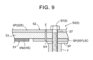
- FIG. 9 is a partial sectional view of a connection terminal surface and a region near conducting through holes of the DC bus board.
- an inverter device 1 is provided in the form of an inverter box 1 A containing a circuit board etc.
- the inverter box 1 A has two cases (inverter cases).
- One of the cases is a base case 1 B to which various components forming inverter circuits 10 shown in FIGS. 3 and 4 and a control board 8 controlling the inverter circuits 10 are attached.
- the other case is a cover case 1 C that contacts the base case 1 B to enclose the inverter circuits 10 and the control board 8 that are attached to the base case 1 B.
- the inverter box 1 A (inverter device 1 ) is formed by enclosing the circuit board etc. by the base case 1 B and the cover case 1 C as the inverter cases.
- a vehicle of the present embodiment is, e.g., a 2-motor split type hybrid vehicle or an in-wheel motor type electric vehicle (or hybrid vehicle), and as shown in FIG. 3 , has two rotating electrical machines MG (MG 1 , MG 2 ) mounted thereon.
- a 2-motor split type hybrid vehicle includes an internal combustion engine and a pair of rotating electrical machines, not shown, as driving force sources.
- a drive device for this hybrid vehicle includes a power distribution differential gear unit (not shown) that distributes output of the internal combustion engine to one of the rotating electrical machines and to wheels and the other rotating electrical machine.
- the in-wheel motor type electric vehicle includes rotating electrical machines as driving force sources in a pair of right and left driving wheels, or includes rotating electrical machines as driving force sources in a power transmission mechanism directly coupled to the driving wheels.
- the inverter box 1 A (inverter device 1 ) is configured as a device that drives the two rotating electrical machines MG (MG 1 , MG 2 ).
- These rotating electrical machines MG (MG 1 , MG 2 ) function as either an electric motor or an electric generator as necessary. That is, these rotating electrical machines MG (MG 1 , MG 2 ) can perform both power running operation and regenerating operation.
- These two rotating electrical machines MG (MG 1 , MG 2 ) are hereinafter simply referred to as the “rotating electrical machines MG” unless they need be identified.
- FIG. 3 shows the system configuration of the rotating electrical machine drive device.
- the rotating electrical machine drive device includes two inverter circuits 10 , namely a first inverter circuit 10 A that drivingly controls one of the rotating electrical machines MG (first rotating electrical machine MG 1 ) and a second inverter circuit 10 B that drivingly controls the other rotating electrical machine MG (second rotating electrical machine MG 2 ).
- the rotating electrical machine drive device further includes a smoothing capacitor 40 that smoothes a system voltage Vdc as a voltage on the DC side of the inverter circuits 10 .
- the inverter circuits 10 ( 10 A, 10 B) and the smoothing capacitor 40 are arranged in the inverter box 1 A.
- the rotating electrical machine drive device sometimes includes a single common converter circuit 18 for the two inverter circuits 10 ( 10 A, 10 B).
- This converter circuit 18 converts DC power (DC voltage) between the common system voltage Vdc for the two inverter circuits 10 ( 10 A, 10 B) and a voltage of a battery 11 .
- the system voltage Vdc is an output voltage (boost-side output voltage) of the converter circuit 18 . If the boost ratio is “1,” the output voltage of the converter circuit 18 is substantially equal to the voltage between terminals of the battery 11 .
- the battery 11 and the converter circuit 18 function as a “DC power supply” of the inverter device 1 .
- the battery 11 functions as the “DC power supply.”
- the smoothing capacitor 40 is connected between a positive electrode P and a negative electrode N of the “DC power supply” thus defined, regardless of whether the rotating electrical machine drive circuit includes the converter circuit 18 or not, and smoothes the voltage between the positive and negative electrodes of the “DC power supply” (system voltage Vdc).
- the battery 11 can supply electric power to the rotating electrical machines MG (MG 1 , MG 2 ) via the two inverter circuits 10 ( 10 A, 10 B), and can store electric power generated by the rotating electrical machines MG (MG 1 , MG 2 ) via the two inverter circuits 10 ( 10 A, 10 B).
- various secondary batteries such as a nickel-metal hydride secondary battery and a lithium-ion secondary battery, capacitors, combinations thereof, etc. are used as such a battery 11 .
- the inverter circuits 10 are circuits that convert DC power having the system voltage Vdc to AC power having a plurality of phases (n phases, where n represents a natural number; in this example, three phases), and supply the AC power to the rotating electrical machines MG (MG 1 , MG 2 ), and that convert AC power generated by the rotating electrical machines MG (MG 1 , MG 2 ) to DC power and supply the DC power to the DC power supply.
- These two inverter circuits 10 ( 10 A, 10 B) are hereinafter simply referred to as the “inverter circuits 10 ” unless they need be identified.
- Each of the inverter circuits 10 has a plurality of switching elements. Insulated gate bipolar transistors (IGBTs) or power metal oxide semiconductor field effect transistors (power MOSFETs) are preferably used as the switching elements. As shown in FIG. 3 , in the present embodiment, IGBTs 30 are used as the switching elements.
- each of the inverter circuits 10 that convert electric power between DC power and three-phase AC power is formed by a bridge circuit having three arms corresponding to the three phases as is well known in the art. That is, as shown in FIGS. 3 and 4 , two IGBTs 30 are connected in series between the DC positive electrode side (positive electrode P side of the DC power supply) and the DC negative electrode side (negative electrode N side of the DC power supply) of the inverter circuit 10 to form a single arm 10 L. Three (three phases: 10 U, 10 V, 10 W) of these series circuits (arms 10 L) are connected in parallel.
- a bridge circuit which has three series circuits (arms 10 L) corresponding to stator coils corresponding to U-phase, V-phase, and W-phase of the rotating electrical machine MG.
- the IGBT 30 in the upper stage of each phase has its collector connected to the positive electrode P of the DC power supply, and has its emitter connected to the collector of the IGBT 30 in the lower stage of that phase.
- the IGBT 30 in the lower stage of each phase has its emitter connected to the negative electrode N of the DC power supply (e.g., the ground).
- Freewheeling diodes (regeneration diodes) are connected in parallel to the IGBTs 30 , respectively. Each freewheeling diode is connected in parallel to a corresponding one of the IGBTs 30 such that its cathode terminal is connected to the collector terminal of the IGBT 30 and its anode terminal is connected to the emitter terminal of the IGBT 30 .
- each arm 10 L in which the IGBTs 30 together with the freewheeling diodes are connected in series is formed as a power module 3 .
- each power module 3 has a positive terminal 3 P that is connected to the positive electrode P of the DC power supply, and a negative terminal 3 N that is connected to the negative electrode N of the DC power supply. That is, each power module 3 is configured by forming at least one arm 10 L that is formed by series connection of at least one IGBT 30 connected to the positive terminal 3 P and at least one IGBT 30 connected to the negative terminal 3 N.
- Each inverter circuit 10 that converts electric power between DC power and three-phase AC power is formed by connecting three of the power modules 3 in parallel.
- the positive terminal 3 P and the negative terminal 3 N are provided as a DC electrode terminal pair 3 T protruding from an end 35 on one side of the power module 3 .
- the inverter circuits 10 are controlled by a control device 80 .
- the control device 80 has an electronic control unit (ECU) and a driver circuit. Part of or all of circuits forming the control device 80 are formed on the control board 8 (see FIG. 1 ).
- the ECU that is mounted on the control device 80 is configured by using a logic circuit such as a microcomputer as a core member.
- the ECU controls the rotating electrical machines MG via the inverter circuits 10 by performing current feedback control by using a vector control method.
- the ECU has various function units for the current feedback control, and each function unit is implemented by cooperation between hardware such as the microcomputer and software (program).
- the IGBTs 30 forming each inverter circuit 10 have their gates connected to the ECU via the driver circuit, and are individually switched on/off.
- the operating voltage power supply voltage of a circuit
- the operating voltage significantly varies between a power electric circuit that drives the rotating electrical machine MG and an electronic circuit such as the ECU using the microcomputer as a core.
- a control signal for the IGBT 30 which is generated by the ECU operating at a relatively low voltage is supplied via the driver circuit to the inverter circuit 10 as a high-voltage gate drive signal S.
- a high-voltage converter gate drive signal SC is similarly supplied from the control device 80 to the converter circuit 18 via the driver circuit.
- FIG. 3 schematically shows a form in which a non-contact type current sensor 12 that is placed near bus bars etc. to detect a current in a non-contact manner detects an actual current of each of the three phases.
- the current sensor 12 is fixed to a third terminal block 93 described below (see FIGS. 1 and 4 ), and detects a current flowing in the bus bars extending in the third terminal block 93 . As shown in FIG.
- a current detection result output connector 9 S is provided on the third terminal block 93 , and is connected to a current detection result input connector 82 of the control board 8 by a cable, not shown, etc.
- the present embodiment shows a configuration in which currents of all the three phases are detected. However, the three phases are in an equilibrium state, and the sum of instantaneous values of the currents is zero. Accordingly, currents of only two phases may be detected by the current sensor 12 , and a current of the remaining one phase may be obtained by computation in the control device 80 .
- the magnetic pole position of a rotor of the rotating electrical machine MG at each time is detected by a rotation sensor 13 , and the control device 80 obtains the detection result.
- the rotation sensor 13 is formed by, e.g., a resolver etc.
- the magnetic pole position represents a rotation angle of the rotor in an electrical angle. As shown in FIG. 3 , the rotation sensor 13 is placed near the rotating electrical machine MG. The detection result of the rotation sensor 13 is therefore transmitted to the control device 80 via a cable, not shown, etc.
- the detection result of the rotation sensor 13 is transmitted to the control device 80 via an external connector 83 that is placed on the control board 8 in order to send and receive signals to and from the outside of the inverter box 1 A.
- Target torque TM (TM 1 , TM 2 ) of the rotating electrical machine MG which is provided to the control device 80 as a request signal from other control device such as a vehicle control device, not shown, is also transmitted via the external connector 83 .
- the control board 8 forming the control device 80 has signal transmission through holes 81 (signal transmission terminal receiving portions) that send and receive signals including the gate drive signal S to and from the power modules 3 .
- signal transmission pins 31 (signal transmission terminals) of the power modules 3 extend through the signal transmission through holes 81 .
- the signal transmission pins 31 are soldered to the signal transmission through holes 81 , whereby signals can be sent between the control board 8 and each power module 3 .
- the signals that are sent between the control board 8 and each power module 3 include a fault diagnosis signal, a temperature detection signal, etc. from the power module 3 to the control board 8 in addition to the gate drive signal S described above.
- the inverter box 1 A is formed by attaching the power modules 3 , a DC bus board 5 having the smoothing capacitor 40 mounted thereon, terminal blocks including a first terminal block 7 (fixing member) (second terminal block 92 and third terminal block 93 ), and the control board 8 to the base case 1 B, and attaching the cover case 1 C to the base case 1 B so as to enclose these components.
- the DC bus board 5 and the first terminal block 7 (fixing member) are common members for the two inverter circuits 10 ( 10 A, 10 B).
- the second terminal block 92 and the third terminal block 93 are provided for each of the first rotating electrical machine MG 1 (first inverter circuit 10 A) and the second rotating electrical machine MG 2 (second inverter circuit 10 B). That is, a first-rotating-electrical-machine second terminal block 92 A and a first-rotating-electrical-machine third terminal block 93 A are provided for the first rotating electrical machine MG 1 , and a second-rotating-electrical-machine second terminal block 92 B and a second-rotating-electrical-machine third terminal block 93 B are provided for the second rotating electrical machine MG 2 .
- the current sensor 12 is fixed to the third terminal block 93 .
- the detection result of the current detected in the first-rotating-electrical-machine third terminal block 93 A is transmitted to the control device 80 via a cable etc., not shown, which connects the current detection result output connector 9 S and a first-rotating-electrical-machine current detection result input connector 82 A of the control board 8 .
- the detection result of the current detected in the second-rotating-electrical-machine third terminal block 93 B is transmitted to the control device 80 via a cable etc., not shown, which connects the current detection result output connector 9 S and a second-rotating-electrical-machine current detection result input connector 82 B of the control board 8 .
- the first terminal block 7 has threaded holes 71 that receive fastening members 97 ( 9 ) extending through fastening member through holes 57 formed in the DC bus board 5 and through holes formed in the DC electrode terminal pairs 3 T of the power modules 3 .
- the base case 1 B has threaded holes 17 a that receive fastening members 95 ( 9 ) extending through holes 72 formed in the first terminal block 7 .
- the first terminal block 7 functions as a fixing member that maintains a relative positional relation between the DC bus board 5 and the plurality of power modules 3 provided corresponding to the arms 10 L corresponding to the plurality of phases of the alternating current.
- a DC electrode pattern connection terminal pair 56 T (see FIGS. 5 and 7 ) connected to the DC power supply are formed on a first board surface 51 of the DC bus board 5 .
- the DC electrode pattern connection terminal pair 56 T are connected to a DC bus board connection terminal pair 76 T formed on the first terminal block 7 as shown in FIG. 6 as a perspective view as viewed from a different direction from FIGS. 1 and 5 . That is, the DC bus board 5 is fastened to the base case 1 B by fastening members 96 ( 9 ) as shown in FIG.
- the first terminal block 7 includes a DC power supply connection terminal pair 75 T that are electrically connected to the DC bus board connection terminal pair 76 T.
- the DC power supply connection terminal pair 75 T are terminals that are connected to the positive electrode P and the negative electrode N of the DC power supply such as the battery 11 placed outside the inverter box 1 A.
- the DC power supply connection terminal pair 75 T are placed outside the inverter box 1 A even in the state where the cover case 1 C is attached to the base case 1 B. The DC power supply connection terminal pair 75 T can thus be easily connected to the DC power supply.
- a first electrode pattern 51 E as one of a positive electrode pattern 5 P and a negative electrode pattern 5 N is formed on the first board surface 51 of the DC bus board 5 which is one of the surfaces of an insulating layer 53 forming a substrate 50
- a second electrode pattern 52 E as the other of the positive electrode pattern 5 P and the negative electrode pattern 5 N is formed on a second board surface 52 of the DC bus board 5 which is the other surface of the insulating layer 53
- the negative electrode pattern 5 N is formed as the first electrode pattern 51 E on the first board surface 51
- the positive electrode pattern 5 P is formed as the second electrode pattern 52 E on the second board surface 52 .
- the electrode patterns of different polarities are formed on the board surfaces. These electrode patterns thus make a DC current flow in opposite directions on these board surfaces. Electromagnetic induction is thus cancelled and mutual inductance increases. This suppresses a surge voltage and reduces loss.
- the positive electrode pattern 5 P and the negative electrode pattern 5 N in which a large current flows have a larger thickness than an electrode layer on a normal printed board, and preferably have a thickness of, e.g., about 300 to 600 [ ⁇ m].
- the electrode pattern diagrams of FIGS. 7 and 8 are diagrams as viewed in the same direction, and one of the electrode pattern diagrams is a front view, and the other is a transparent view.
- FIG. 8 is a diagram of the DC bus board 5 as directly viewed from the second board surface 52 (the soldering surface described below) side (a front view of the second board surface 52 )
- FIG. 7 is a diagram of the first board surface 51 of the DC bus board 5 as transparently viewed from the second board surface 52 side (a transparent view of the first board surface 51 ).
- each terminal of the DC bus board 5 specifically the connection positive terminals 55 P, the connection negative terminals 55 N, and the DC electrode pattern connection terminal pair 56 T are formed on the first board surface 51 of the DC bus board 5 .
- the DC bus board 5 is fixed to the first terminal block 7 by the fastening members 9 such that the first board surface 51 contacts terminals provided on other members such as the power modules 3 and the first terminal block 7 .
- the DC bus board 5 is fastened to the base case 1 B via the first terminal block 7 by the fastening members 9 such that the terminals provided on the first board surface 51 contact the terminals provided on other members.
- each of these terminals includes a connection terminal surface 5 C formed on the first board surface 51 so as to be separated from the first electrode pattern 51 E (negative electrode pattern 5 N), and conducting through holes 5 H extending through the insulating layer 53 .
- the conducting through holes 5 H are formed separately from the fastening member through hole 57 in the connection positive terminal 55 P through which the fastening member 9 extends.
- Each conducting through hole 5 H has a conductive material E on its inner wall, and the second electrode pattern 52 E (positive electrode pattern 5 P) is electrically connected to the connection terminal surface 5 C by the conductive material E.
- FIG. 9 shows a section taken along line IX-IX in FIG. 7 in the state where the DC bus board 5 together with the power modules 3 is fixed to the first terminal block 7 by the fastening members 9 ( 97 ).
- connection positive terminals 55 P, the connection negative terminals 55 N, and the DC electrode pattern connection terminal pair 56 T are insulated by coating the board surfaces with resist etc.
- the conducting through holes 5 H are not subjected to an insulation treatment so that the conducting through holes 5 H can be filled with solder in a flow process described below. Filling the conducting through holes 5 H with solder increases a sectional area of electrical connection, and can reduce impedance between the first board surface 51 and the second board surface 52 .
- Bolts made of a conductive metal such as iron, etc. are often used as the fastening members 9 . Accordingly, when a current flows between the first board surface 51 and the second board surface 52 of the DC bus board 5 , the current also flows in the fastening members 9 , which may increase the temperature of the terminals (DC electrode terminal pairs 3 T) of the power modules 3 and the peripheries thereof due to the heat generated by the fastening members 9 .
- the conducting through holes 5 H having the conductive material E on their inner walls are provided separately from the fastening member through holes 57 as described above, most of the current flows between the first board surface 51 and the second board surface 52 of the DC bus board 5 via the conducting through holes 5 H having lower impedance.
- Providing the conducting through holes 5 H in this manner allows non-conductive members (made of a resin etc.) to be used as the fastening members 9 . Accordingly, flexibility in selection of components is improved.
- the members made of a resin are typically lighter than members made of iron, and thus contribute to reduction in weight of the inverter box 1 A.
- the conductive material E may be provided on the inner walls of the fastening member through holes 57 by plating etc., or the conductive material E may not be provided on the inner walls of the fastening member through holes 57 . In the form exemplarily shown in FIG. 9 , the conductive material E is not provided on the inner walls of the fastening member through holes 57 .
- FIGS. 7 to 9 show an example in which the negative electrode pattern 5 N is formed as the first electrode pattern 51 E on the first board surface 51 and the positive electrode pattern 5 P is formed as the second electrode pattern 52 E on the second board surface 52 , the positive electrode pattern 5 P may be formed as the first electrode pattern 51 E and the negative electrode pattern 5 N may be formed as the second electrode pattern 52 E.
- the smoothing capacitor 40 is formed by parallel connection of a plurality of capacitor elements 4 .
- the number of capacitor elements 4 corresponds to that of power modules 3 , and the capacitor elements 4 are arranged and distributed so as to have a positional relation corresponding to that of the power modules 3 .
- the power modules 3 are placed on both sides of the smoothing capacitor 40 (capacitor element group) as viewed in a direction perpendicular to the board surface of the DC bus board 5 .
- the plurality of power modules 3 provided corresponding to the arms 10 L corresponding to the plurality of phases of the alternating current are arranged in line along one end surface 5 L of the DC bus board 5 .
- the power modules 3 are arranged in line along each of opposing two end surfaces 5 L.
- the number of capacitor elements 4 corresponds to the number of power modules 3 .
- one or more capacitor elements 4 are provided for each power module 3 . That is, the number of capacitor elements 4 is the same as that of power modules 3 , or is equal to the number of power modules 3 multiplied by a natural number.
- the capacitor elements 4 are arranged so as to have a positional relation corresponding to that of the power modules 3 . For example, the capacitor elements 4 are placed near each power module 3 .
- each power module connection terminal pair 55 T as a pair of connection positive terminal 55 P and connection negative terminal 55 N, the capacitor element 4 is placed so as to have such an arrangement distance (capacitor arrangement distance) that the distance between the capacitor element 4 and the connection positive terminal 55 P is equal to (substantially the same as) that between the capacitor element 4 and the connection negative terminal 55 N.
- the capacitor elements 4 are arranged and distributed so that the capacitor arrangement distances for all the power modules 3 are equal to each other (substantially the same).
- the distances to the connection positive terminal 55 P and the distances to the connection negative terminal 55 N are preferably average values.
- the capacitor elements 4 are arranged in this manner, the capacitor elements 4 are located near each power module 3 as a result. This reduces the impedance (especially an inductance component) of each power module 3 (each arm 10 L) to the DC power supply, and can satisfactorily suppress a surge voltage that is generated by switching of the IGBTs 30 .
- a discharge resistor R (see FIG. 4 ) is often provided parallel to the smoothing capacitor 40 in order to discharge the remaining charge upon shutdown of the rotating electrical machine drive device.
- This discharge resistor R can also be mounted on the DC bus board 5 .
- the discharge resistor R and its fixing mechanism need not be placed at other positions in the inverter box 1 A, and reduction in size can be implemented.
- the DC electrode pattern connection terminal pair 56 T that is electrically connected to the DC bus board connection terminal pair 76 T electrically connected to the DC power supply connection terminal pair 75 T electrically connected to the external DC power supply is formed on the DC bus board 5 .
- the discharge resistor R is preferably placed near the DC electrode pattern connection terminal pair 56 , e.g., so as to adjoin this terminal pair.
- the discharge resistor R can also be formed by parallel connection of a plurality of smaller resistive elements (not shown) having small current capacity.
- the first board surface 51 of the DC bus board 5 is a component surface on which the plurality of capacitor elements 4 and the resistive elements are mounted.
- the example shown in FIGS. 7 and 8 shows a form in which only the capacitor elements 4 are mounted thereon.
- the capacitor elements 4 are electric field capacitors.
- the capacitor elements 4 are radial discrete components.
- lead wires functioning as terminals of the capacitor elements 4 extend to the second board surface 52 side through holes formed in the DC bus board 5 .
- the lead wires of the capacitor elements 4 are soldered to the second board surface 52 .
- the second board surface 52 is therefore a soldering surface on which soldering is performed.
- This soldering is often performed by a flow process in which the DC bus board 5 is moved so that the soldering surface extends along the liquid surface of a solder bath filed with molten solder.
- the lead wires of the capacitor elements 4 mounted on the component surface protrude beyond the soldering surface via the through holes.
- the lead wires protruding beyond the soldering surface are soldered to lands (conductive material E) formed around the through holes and the conductive material E formed on the inner walls of the through holes. At this time, no solder adheres to the conductive material E (the lands, the through holes, etc.) insulated by resist etc.
- the conducting through holes 5 H are not subjected to an insulation treatment such as a resist treatment, so that solder can be guided toward the first board surface 51 (component surface) via the conducting through holes 5 H by using capillarity in the flow process and the conducting through holes 5 H can be filled with solder.
- the through holes in which the lead wires of the capacitor elements 4 are inserted are also not subjected to an insulation treatment such as a resist treatment, and therefore solder is guided toward the first board surface 51 by capillarity via the through holes and the lead wires.
- the lead wires are soldered to both surfaces of the DC bus board 5 . Accordingly, mechanical connection is obtained, and electrically reliable mounting is implemented.
- the lead wire connection lands (electrode pattern) that are formed in the first electrode pattern 51 E (negative electrode pattern 5 N) on the first board surface 51 have a large area as they are, solder may be solidified before reaching the first board surface 51 because heat dissipates. Accordingly, solder may not sufficiently move up to the first board surface 51 . It is therefore preferable that these lands be shaped so that the conductive material E is partially omitted, as shown by reference character “ 54 N” in FIG. 7 .
- the DC bus board 5 is brought into contact with molten solder having a temperature of 200° C. or higher, and therefore the temperature of the DC bus board 5 also increases. If the capacitor elements 4 are electric field capacitors, their outer casings (sleeves) may partially melt, and their insulation properties may be degraded. In the form in which the negative electrode pattern 5 N is formed on the component surface (first board surface 51 ), the polarity (negative electrode N) of the sleeves is the same as that of the negative electrode pattern 5 N. Accordingly, reliability is not reduced even if the insulation properties are degraded.
- the DC bus board 5 has the connection positive terminals 55 P that are electrically connected to the positive electrode pattern 5 P and the connection negative terminals 55 N that are electrically connected to the negative electrode pattern 5 N.
- the connection positive terminal 55 P is a terminal that is to be electrically connected to the positive terminal 3 P of the power module 3 when the inverter box 1 A is assembled as shown in FIGS. 1 and 5 .
- the connection negative terminal 55 N is a terminal that is to be electrically connected to the negative terminal 3 N of the power module 3 .
- the DC bus board 5 has a plurality of connection positive terminals 55 N that are electrically connected to the positive electrode pattern 5 P and that are respectively electrically connected to the positive terminals 3 P of the plurality of power modules 3 , and a plurality of connection negative terminals 55 N that are electrically connected to the negative electrode pattern 5 N and that are respectively electrically connected to the negative terminals 3 N of the plurality of power modules 3 .
- connection positive terminal 55 N and the positive terminal 3 P which correspond to each other are fastened to the first terminal block 7 (fixing member) by a common fastening member 97 ( 9 ), and the connection negative terminal 55 N and the negative terminal 3 N which correspond to each other are fastened to the first terminal block 7 (fixing member) by a common fastening member 97 ( 9 ), so that the DC bus board 5 and the power modules 3 are fixed to the first terminal block 7 (fixing member).
- the connection positive terminals 55 P of the DC bus board 5 and the positive terminals 3 P of the power modules 3 are fastened to the first terminal block 7 (fixing member) by the common fastening members 97 ( 9 ).
- connection negative terminals 55 N of the DC bus board 5 and the negative terminals 3 N of the power modules 3 are fastened to the first terminal block 7 (fixing member) by the common fastening members 97 ( 9 ).
- the DC bus board 5 and the power modules 3 are thus fixed to the first terminal block 7 (fixing member).
- the positive terminal 3 P and the negative terminal 3 N of each power module 3 are provided as a DC electrode terminal pair 3 T protruding from the end 35 on one side of the power module 3 .
- Each power module 3 is fixed such that the end 35 on one side faces the first terminal block 7 (fixing member).
- the DC electrode pattern connection terminal pair 56 T formed on the DC bus board 5 is fastened to the first terminal block 7 by the fastening members 96 ( 9 ) so as to be in contact with the DC bus board connection terminal pair 76 T of the first terminal block 7 .
- the power module 3 is fixed more firmly. Since each power module 3 can be made to more closely contact the base case 1 B, the power module 3 can be cooled via the base case 1 B.
- the base case 1 B have cooling fins on the surface opposite to the surface that contacts the power modules 3 .
- the power modules 3 can be satisfactorily cooled by using the base case 1 B as a heat sink.
- the inverter box 1 A of the present embodiment has two inverter circuits 10 ( 10 A, 10 B) that convert electric power between three-phase AC power and DC power.
- the inverter box 1 A is formed by placing the power modules 3 of the inverter circuits 10 ( 10 A, 10 B) on respective sides of the DC bus board 5 as viewed in the direction perpendicular to the board surface of the DC bus board 5 .
- the control board 8 on which part of or all of the circuits of the control device 80 controlling the two inverter circuits 10 ( 10 A, 10 B) are formed is placed so as to cover the power modules 3 and the DC bus board 5 as viewed in the direction perpendicular to the board surface of the DC bus board 5 .
- the control board 8 is therefore a substrate having a relatively large area, and is preferably sufficiently fixed so as to suppress warping, vibration, etc.
- the base case 1 B (inverter case) that accommodates the DC bus board 5 , the power modules 3 , and the first terminal block 7 (fixing member) has a support 19 that supports and fixes the control board 8 in the central portion of the control board 8 .
- the DC bus board 5 that is to be located on the central portion of the control board 8 in the assembled state of the inverter box 1 A as viewed in the direction perpendicular to the board surface has a support through hole 59 through which the support 19 extends.
- the support through hole 59 is provided between the phases of the capacitor elements arranged so as to correspond to the power modules 3 that are arranged in line along one end surface 5 L of the DC bus board 5 and that form the n-phase arms 10 L ( 10 U, 10 V, 10 V).
- the support through hole 59 is formed at two positions that are located between the phases of the capacitor elements 4 that are arranged and distributed at three positions so as to correspond to the three power modules 3 of the inverter circuit 10 that converts electric power between three-phase AC power and DC power.
- the two supports 19 that are provided in the base case 1 B are formed so as to correspond to the support through holes 59 formed at the two positions.
- the inverter circuit 10 that converts electric power between three-phase AC power and DC power.
- the inverter circuit 10 is a circuit that converts electric power between n-phase AC power and DC power, where n represents a natural number
- the DC bus board 5 have the support through hole 59 at (n ⁇ 1) positions each located between the phases of the capacitor elements 4 arranged and distributed so as to correspond to the power modules 3 that are arranged in line along one end surface 5 L of the DC bus board 5 and that form the n-phase arms 10 L.
- Providing the support though holes 59 in the DC bus board 5 eliminates the need to provide a separate fixing support structure for the control board 8 , and can reduce the size of the inverter box 1 A.
- the DC electrode terminal pairs 3 T are provided so as to protrude from the ends 35 on one side of the power modules 3 .
- AC electrode terminals 3 C corresponding to the arms 10 L are provided so as to protrude from ends 33 located on the opposite side to the ends 35 on one side (see FIGS. 1 and 5 ).
- Each second terminal block 92 has three fixing portions in order to fix all of the three-phase AC electrode terminals 3 C.
- Each third terminal block 93 has three-phase AC relay terminals 9 C that are connected to all of the three-phase AC electrode terminals 3 C.
- the AC electrode terminals 3 C of the power modules 3 are fastened to the AC relay terminals 9 C of the third terminal block 93 and the second terminal block 92 by common fastening members 9 .
- Each second terminal block 92 is fastened and fixed to threaded holes 17 c formed in the base case 1 B by the fastening members 9
- each third terminal block 93 is fastened and fixed to threaded holes 17 d formed in the base case 1 B by fastening members 9 .
- each third terminal block 93 includes three AC output terminals 9 T corresponding to the three-phase AC relay terminals 9 C.
- the AC relay terminal 9 C and the AC output terminal 9 T of each phase are connected by the bus bar extending through the third terminal block 93 .
- Each third terminal block 93 is provided with the current sensor 12 that detects a current in the bus bars in a non-contact manner, as described above.
- the AC output terminals 9 T are located outside the inverter box 1 A even in the state where the cover case 1 C is attached to the base case 1 B. This allows the AC output terminals 9 T to be satisfactorily connected to the stator coils of each phase of each rotating electrical machine MG.
- the control board 8 is fixed to the base case 1 B by fastening members 9 so as to cover these components.
- the signal transmission pins 31 of the power modules 3 extend through the signal transmission through holes 81 of the control board 8 .
- the signal transmission pins 31 are soldered to the signal transmission through holes 81 .
- the inverter box 1 A (inverter device 1 ) may include a single inverter circuit 10 or may include three or more inverter circuits 10 .
- any number of inverter circuits 10 may be provided as long as the DC bus board 5 and the power modules 3 are fixed to the first terminal block 7 by fastening the connection positive terminals 55 P of the DC bus board 5 and the positive terminals 3 P of the power modules 3 to the first terminal block 7 (fixing member) by the common fastening members 9 and fastening the connection negative terminals 55 N of the DC bus board 5 and the negative terminals 3 N of the power modules 3 to the first terminal block 7 by the common fastening members 9 .
- the positive terminal 3 P and the negative terminal 3 N of each power module 3 be provided as a DC electrode terminal pair 3 T protruding from the end 35 on one side of the power module 3 , as described above.
- the manner in which the DC bus board 5 and the power modules 3 are connected is not limited to this form.
- the DC bus board 5 and the power modules 3 may be connected such that the DC bus board 5 and the main body of each power module 3 overlap each other (partially or entirely overlap each other) as viewed in the direction perpendicular to the board surface of the DC bus board 5 .
- the positive terminal 3 P and the negative terminal 3 N may not be provided as a pair in the same part of the power module 3 .
- the power modules 3 can be placed only on one side of the DC bus board 5 .
- the inverter box 1 A can be formed by either the power modules 3 forming the first inverter circuit 10 A or the power modules 3 forming the second inverter circuit 10 B in FIG. 1 .
- the power modules 3 are not placed on both sides of the smoothing capacitor 40 but placed on one side of the smoothing capacitor 40 as viewed in the direction perpendicular to the board surface of the DC bus board 5 .
- the power modules 3 may thus be placed on one side.
- the power modules 3 may be placed on both sides of the smoothing capacitor 40 as viewed in the direction perpendicular to the board surface of the DC bus board 5 .
- the power modules 3 can be placed on both sides of the smoothing capacitor 40 by placing on one side of the smoothing capacitor 40 one of the three-phase power modules 3 of the inverter circuit 10 that converts electric power between three-phase AC power and DC power, and placing the remaining two power modules 3 on the other side of the smoothing capacitor 40 .
- the smoothing capacitor 40 is formed by parallel connection of a plurality of capacitor elements 4 , the number of capacitor elements 4 corresponds to the number of power modules 3 , and the capacitor elements 4 are arranged so as to have a positional relation corresponding to that of the power modules 3 .
- the capacitor elements 4 may be arranged and distributed independently of the arrangement of the power modules 3 . Even if the power modules 3 corresponding to the phases are aligned as described above, the capacitor elements 4 may be arranged and distributed independently of the arrangement of the power modules 3 .
- the smoothing capacitor 40 is formed by parallel connection of a plurality of capacitor elements 4 .
- the smoothing capacitor 40 may be formed by a single element.
- electrolytic capacitors are exemplarily shown as the capacitor elements 4 .
- elements having other structures such as film capacitors may be used as the capacitor elements 4 .
- the present invention can be used for inverter devices that include a power module having a switching element and a smoothing capacitor, and that convert electric power between DC power and AC power.
Applications Claiming Priority (3)
| Application Number | Priority Date | Filing Date | Title |
|---|---|---|---|
| JP2012125115A JP5796257B2 (ja) | 2012-05-31 | 2012-05-31 | インバータ装置 |
| JP2012-125115 | 2012-05-31 | ||
| PCT/JP2013/063293 WO2013179880A1 (ja) | 2012-05-31 | 2013-05-13 | インバータ装置 |
Publications (2)
| Publication Number | Publication Date |
|---|---|
| US20150340966A1 US20150340966A1 (en) | 2015-11-26 |
| US9425707B2 true US9425707B2 (en) | 2016-08-23 |
Family
ID=49673083
Family Applications (1)
| Application Number | Title | Priority Date | Filing Date |
|---|---|---|---|
| US14/396,893 Active 2033-10-04 US9425707B2 (en) | 2012-05-31 | 2013-05-13 | Inverter device capable of appropriately fixing a power module having a switching element and a smoothing capacitor in a limited region |
Country Status (5)
| Country | Link |
|---|---|
| US (1) | US9425707B2 (ja) |
| JP (1) | JP5796257B2 (ja) |
| CN (1) | CN104272575B (ja) |
| DE (1) | DE112013001936T5 (ja) |
| WO (1) | WO2013179880A1 (ja) |
Cited By (1)
| Publication number | Priority date | Publication date | Assignee | Title |
|---|---|---|---|---|
| US11088649B2 (en) * | 2017-04-27 | 2021-08-10 | Mitsubishi Electric Corporation | Power conversion unit |
Families Citing this family (24)
| Publication number | Priority date | Publication date | Assignee | Title |
|---|---|---|---|---|
| JP5862606B2 (ja) * | 2013-05-17 | 2016-02-16 | 株式会社デンソー | 電力変換装置 |
| CN204011078U (zh) * | 2014-04-22 | 2014-12-10 | 比亚迪股份有限公司 | 电动汽车及其电容器 |
| WO2015187680A1 (en) * | 2014-06-03 | 2015-12-10 | Cummins Power Generation Ip, Inc. | Modular inverter platform providing physical and electrical configurability and scalability |
| JP6146380B2 (ja) | 2014-07-31 | 2017-06-14 | 株式会社デンソー | 電子装置 |
| JP2016092995A (ja) * | 2014-11-06 | 2016-05-23 | Ntn株式会社 | インホイールモータ装置およびそのインホイールモータ制御装置 |
| JP6348460B2 (ja) * | 2015-07-08 | 2018-06-27 | 東芝三菱電機産業システム株式会社 | 電力変換システム |
| JP6595269B2 (ja) * | 2015-09-07 | 2019-10-23 | 日立オートモティブシステムズ株式会社 | 電動駆動装置及び電動パワーステアリング装置 |
| JP6610944B2 (ja) * | 2015-12-18 | 2019-11-27 | 株式会社デンソー | 制御装置一体型回転電機 |
| JP6418196B2 (ja) | 2016-04-15 | 2018-11-07 | トヨタ自動車株式会社 | 電気自動車 |
| EP3540932B1 (en) * | 2016-11-11 | 2020-10-07 | Mitsubishi Electric Corporation | Power conversion device and air conditioning device using same |
| DE112018000455T5 (de) * | 2017-03-30 | 2019-10-02 | Aisin Aw Co., Ltd. | Invertereinheit |
| JP6504622B2 (ja) | 2017-06-14 | 2019-04-24 | 三菱電機株式会社 | 開閉モジュール用のコンデンサ基板ユニット、開閉モジュール、およびモータ駆動装置 |
| JP2019067896A (ja) * | 2017-09-29 | 2019-04-25 | 日本電産エレシス株式会社 | 回路基板、および制御装置 |
| FR3076175B1 (fr) * | 2017-12-22 | 2020-01-10 | Valeo Siemens Eautomotive France Sas | Equipement electrique a paroi deportee |
| JP6984398B2 (ja) * | 2017-12-22 | 2021-12-22 | トヨタ自動車株式会社 | パワーコントロールユニット |
| JP7147171B2 (ja) * | 2018-01-31 | 2022-10-05 | 株式会社アイシン | 回路基板、回路ユニット、インバータ装置、及び回路基板の検査方法 |
| US10600577B2 (en) * | 2018-04-26 | 2020-03-24 | Sf Motors, Inc. | Electric vehicle inverter module capacitors |
| US10581357B2 (en) * | 2018-05-11 | 2020-03-03 | Abb Schweiz Ag | Rotating direct current power supply for synchronous machines |
| US10447170B1 (en) * | 2018-11-09 | 2019-10-15 | Sf Motors, Inc. | Inverter module for drivetrain of an electric vehicle |
| EP3703238A1 (en) * | 2019-02-28 | 2020-09-02 | ABB Schweiz AG | An inverter for a photovoltaic plant |
| CN112838743B (zh) * | 2019-11-22 | 2022-03-29 | 英业达科技有限公司 | 电源供应装置 |
| DE102019132685B4 (de) * | 2019-12-02 | 2022-05-25 | Audi Ag | Elektrische Schaltungsanordnung umfassend eine Erregerschaltung und eine Inverterschaltung und Kraftfahrzeug |
| JP7405671B2 (ja) * | 2020-03-30 | 2023-12-26 | 日立Astemo株式会社 | 電力変換装置 |
| JP2023049781A (ja) * | 2021-09-29 | 2023-04-10 | 本田技研工業株式会社 | 電力変換装置 |
Citations (20)
| Publication number | Priority date | Publication date | Assignee | Title |
|---|---|---|---|---|
| US5497289A (en) * | 1992-09-30 | 1996-03-05 | Mitsubishi Denki Kabushiki Kaisha | Inverter apparatus and method therefor |
| US20040257841A1 (en) * | 2003-06-18 | 2004-12-23 | Aisin Aw Co., Ltd. | Device for removing inverter noise |
| JP2005328651A (ja) | 2004-05-14 | 2005-11-24 | Mitsubishi Electric Corp | 電力変換装置 |
| JP2005347561A (ja) | 2004-06-03 | 2005-12-15 | Toshiba Corp | パワー半導体モジュールおよび電力変換装置 |
| US20070109715A1 (en) | 2005-11-17 | 2007-05-17 | Hitachi, Ltd. | Capacitor module, power converter, vehicle-mounted electrical-mechanical system |
| JP2009106046A (ja) | 2007-10-23 | 2009-05-14 | Hitachi Ltd | 自動車用電力変換装置 |
| JP2009106074A (ja) | 2007-10-23 | 2009-05-14 | Aisin Aw Co Ltd | インバータ装置 |
| JP2009177872A (ja) | 2008-01-22 | 2009-08-06 | Nissan Motor Co Ltd | 電力変換装置および電力変換装置の製造方法 |
| JP2009213269A (ja) | 2008-03-04 | 2009-09-17 | Toyota Industries Corp | 電力変換装置 |
| US20090251875A1 (en) | 2008-03-04 | 2009-10-08 | Kabushiki Kaisha Toyota Jidoshokki | Power converter apparatus |
| JP2010104135A (ja) | 2008-10-23 | 2010-05-06 | Hitachi Ltd | 電力変換装置及び車載用電機システム |
| JP2010288328A (ja) | 2009-06-09 | 2010-12-24 | Mitsubishi Electric Corp | 電子制御装置 |
| US20110069466A1 (en) * | 2009-09-21 | 2011-03-24 | Gm Global Technology Operations, Inc. | Low inductance power electronics assembly |
| US20110148337A1 (en) * | 2007-09-12 | 2011-06-23 | Aisin Seiki Kabushiki Kaisha | Power semiconductor chip, power semiconductor module, inverter apparatus, and inverter-integrated motor |
| JP2011135769A (ja) | 2009-11-25 | 2011-07-07 | Daikin Industries Ltd | 電力変換装置 |
| US20110261600A1 (en) * | 2010-01-22 | 2011-10-27 | Denso Corporation | Power conversion apparatus |
| US20120045353A1 (en) * | 2009-09-24 | 2012-02-23 | Mitsubishi Heavy Industries, Ltd. | Inverter-integrated electric compressor |
| JP2012070570A (ja) | 2010-09-24 | 2012-04-05 | Aisin Aw Co Ltd | 電力変換装置 |
| JP2012070632A (ja) | 2012-01-06 | 2012-04-05 | Hitachi Automotive Systems Ltd | 電力変換装置 |
| JP2012147596A (ja) | 2011-01-13 | 2012-08-02 | Aisin Aw Co Ltd | 半導体装置 |
Family Cites Families (2)
| Publication number | Priority date | Publication date | Assignee | Title |
|---|---|---|---|---|
| JP3975394B2 (ja) * | 2001-12-27 | 2007-09-12 | アイシン・エィ・ダブリュ株式会社 | 電動駆動装置制御ユニット |
| JP4398305B2 (ja) * | 2004-06-02 | 2010-01-13 | カシオ計算機株式会社 | 半導体装置およびその製造方法 |
-
2012
- 2012-05-31 JP JP2012125115A patent/JP5796257B2/ja active Active
-
2013
- 2013-05-13 WO PCT/JP2013/063293 patent/WO2013179880A1/ja active Application Filing
- 2013-05-13 CN CN201380022848.8A patent/CN104272575B/zh active Active
- 2013-05-13 US US14/396,893 patent/US9425707B2/en active Active
- 2013-05-13 DE DE112013001936.1T patent/DE112013001936T5/de active Pending
Patent Citations (23)
| Publication number | Priority date | Publication date | Assignee | Title |
|---|---|---|---|---|
| US5497289A (en) * | 1992-09-30 | 1996-03-05 | Mitsubishi Denki Kabushiki Kaisha | Inverter apparatus and method therefor |
| US20040257841A1 (en) * | 2003-06-18 | 2004-12-23 | Aisin Aw Co., Ltd. | Device for removing inverter noise |
| JP2005328651A (ja) | 2004-05-14 | 2005-11-24 | Mitsubishi Electric Corp | 電力変換装置 |
| JP2005347561A (ja) | 2004-06-03 | 2005-12-15 | Toshiba Corp | パワー半導体モジュールおよび電力変換装置 |
| US20070109715A1 (en) | 2005-11-17 | 2007-05-17 | Hitachi, Ltd. | Capacitor module, power converter, vehicle-mounted electrical-mechanical system |
| JP2007143272A (ja) | 2005-11-17 | 2007-06-07 | Hitachi Ltd | コンデンサモジュール,電力変換装置及び車載用電機システム |
| US20110148337A1 (en) * | 2007-09-12 | 2011-06-23 | Aisin Seiki Kabushiki Kaisha | Power semiconductor chip, power semiconductor module, inverter apparatus, and inverter-integrated motor |
| JP2009106046A (ja) | 2007-10-23 | 2009-05-14 | Hitachi Ltd | 自動車用電力変換装置 |
| JP2009106074A (ja) | 2007-10-23 | 2009-05-14 | Aisin Aw Co Ltd | インバータ装置 |
| JP2009177872A (ja) | 2008-01-22 | 2009-08-06 | Nissan Motor Co Ltd | 電力変換装置および電力変換装置の製造方法 |
| US20090251875A1 (en) | 2008-03-04 | 2009-10-08 | Kabushiki Kaisha Toyota Jidoshokki | Power converter apparatus |
| JP2009213269A (ja) | 2008-03-04 | 2009-09-17 | Toyota Industries Corp | 電力変換装置 |
| JP2010104135A (ja) | 2008-10-23 | 2010-05-06 | Hitachi Ltd | 電力変換装置及び車載用電機システム |
| US20110221268A1 (en) | 2008-10-23 | 2011-09-15 | Hitachi, Ltd. | Power Converter and In-Car Electrical System |
| JP2010288328A (ja) | 2009-06-09 | 2010-12-24 | Mitsubishi Electric Corp | 電子制御装置 |
| US20110069466A1 (en) * | 2009-09-21 | 2011-03-24 | Gm Global Technology Operations, Inc. | Low inductance power electronics assembly |
| US20120045353A1 (en) * | 2009-09-24 | 2012-02-23 | Mitsubishi Heavy Industries, Ltd. | Inverter-integrated electric compressor |
| JP2011135769A (ja) | 2009-11-25 | 2011-07-07 | Daikin Industries Ltd | 電力変換装置 |
| US20110261600A1 (en) * | 2010-01-22 | 2011-10-27 | Denso Corporation | Power conversion apparatus |
| JP2012070570A (ja) | 2010-09-24 | 2012-04-05 | Aisin Aw Co Ltd | 電力変換装置 |
| JP2012147596A (ja) | 2011-01-13 | 2012-08-02 | Aisin Aw Co Ltd | 半導体装置 |
| US8829669B2 (en) | 2011-01-13 | 2014-09-09 | Aisin Aw Co., Ltd. | Semiconductor device |
| JP2012070632A (ja) | 2012-01-06 | 2012-04-05 | Hitachi Automotive Systems Ltd | 電力変換装置 |
Cited By (1)
| Publication number | Priority date | Publication date | Assignee | Title |
|---|---|---|---|---|
| US11088649B2 (en) * | 2017-04-27 | 2021-08-10 | Mitsubishi Electric Corporation | Power conversion unit |
Also Published As
| Publication number | Publication date |
|---|---|
| JP2013251991A (ja) | 2013-12-12 |
| US20150340966A1 (en) | 2015-11-26 |
| JP5796257B2 (ja) | 2015-10-21 |
| CN104272575B (zh) | 2017-03-08 |
| CN104272575A (zh) | 2015-01-07 |
| WO2013179880A1 (ja) | 2013-12-05 |
| DE112013001936T5 (de) | 2014-12-24 |
Similar Documents
| Publication | Publication Date | Title |
|---|---|---|
| US9425707B2 (en) | Inverter device capable of appropriately fixing a power module having a switching element and a smoothing capacitor in a limited region | |
| US10106189B2 (en) | Motor drive control device for electric power steering | |
| EP2605391B1 (en) | Power inverter | |
| US9654046B2 (en) | Reduced size power inverter suitable for a vehicle | |
| US9159506B2 (en) | Capacitor module and power conversion device | |
| US7561448B2 (en) | Power inverter | |
| US8212382B2 (en) | Power conversion apparatus and electric vehicle | |
| US9859810B2 (en) | Power converter | |
| EP1861915B1 (en) | Power module | |
| US20140140119A1 (en) | Power Inverter | |
| US10381922B2 (en) | Power converter | |
| US11424689B2 (en) | Power conversion device | |
| CN112260560B (zh) | 电力变换装置 | |
| WO2016186087A1 (ja) | コンデンサモジュール | |
| JP6830214B2 (ja) | 電力変換装置 | |
| US20230328938A1 (en) | Power module | |
| JP2021180541A (ja) | 電力変換装置 |
Legal Events
| Date | Code | Title | Description |
|---|---|---|---|
| AS | Assignment |
Owner name: AISIN AW CO., LTD., JAPAN Free format text: ASSIGNMENT OF ASSIGNORS INTEREST;ASSIGNORS:MUTSUURA, KEITA;KONDO, TATSUYA;MORITA, MAKOTO;SIGNING DATES FROM 20140905 TO 20141019;REEL/FRAME:034028/0188 Owner name: TOYOTA JIDOSHA KABUSHIKI KAISHA, JAPAN Free format text: ASSIGNMENT OF ASSIGNORS INTEREST;ASSIGNORS:MUTSUURA, KEITA;KONDO, TATSUYA;MORITA, MAKOTO;SIGNING DATES FROM 20140905 TO 20141019;REEL/FRAME:034028/0188 |
|
| STCF | Information on status: patent grant |
Free format text: PATENTED CASE |
|
| MAFP | Maintenance fee payment |
Free format text: PAYMENT OF MAINTENANCE FEE, 4TH YEAR, LARGE ENTITY (ORIGINAL EVENT CODE: M1551); ENTITY STATUS OF PATENT OWNER: LARGE ENTITY Year of fee payment: 4 |
|
| AS | Assignment |
Owner name: TOYOTA JIDOSHA KABUSHIKI KAISHA, JAPAN Free format text: NUNC PRO TUNC ASSIGNMENT;ASSIGNOR:AISIN AW CO., LTD.;REEL/FRAME:062034/0244 Effective date: 20221021 |
|
| AS | Assignment |
Owner name: TOYOTA JIDOSHA KABUSHIKI KAISHA, JAPAN Free format text: NUNC PRO TUNC ASSIGNMENT;ASSIGNOR:TOYOTA JIDOSHA KABUSHIKI KAISHA;REEL/FRAME:062241/0670 Effective date: 20221124 Owner name: DENSO CORPORATION, JAPAN Free format text: NUNC PRO TUNC ASSIGNMENT;ASSIGNOR:TOYOTA JIDOSHA KABUSHIKI KAISHA;REEL/FRAME:062241/0670 Effective date: 20221124 |
|
| MAFP | Maintenance fee payment |
Free format text: PAYMENT OF MAINTENANCE FEE, 8TH YEAR, LARGE ENTITY (ORIGINAL EVENT CODE: M1552); ENTITY STATUS OF PATENT OWNER: LARGE ENTITY Year of fee payment: 8 |