US9373595B2 - Mounting structure and manufacturing method for same - Google Patents
Mounting structure and manufacturing method for same Download PDFInfo
- Publication number
- US9373595B2 US9373595B2 US14/342,935 US201214342935A US9373595B2 US 9373595 B2 US9373595 B2 US 9373595B2 US 201214342935 A US201214342935 A US 201214342935A US 9373595 B2 US9373595 B2 US 9373595B2
- Authority
- US
- United States
- Prior art keywords
- electrode
- solder
- semiconductor chip
- mounting structure
- alloy
- Prior art date
- Legal status (The legal status is an assumption and is not a legal conclusion. Google has not performed a legal analysis and makes no representation as to the accuracy of the status listed.)
- Active
Links
- 238000004519 manufacturing process Methods 0.000 title description 66
- 229910045601 alloy Inorganic materials 0.000 claims abstract description 244
- 239000000956 alloy Substances 0.000 claims abstract description 244
- 229910052751 metal Inorganic materials 0.000 claims abstract description 113
- 239000002184 metal Substances 0.000 claims abstract description 113
- 239000000758 substrate Substances 0.000 claims abstract description 20
- 229910000679 solder Inorganic materials 0.000 claims description 261
- PXHVJJICTQNCMI-UHFFFAOYSA-N Nickel Chemical compound [Ni] PXHVJJICTQNCMI-UHFFFAOYSA-N 0.000 claims description 63
- 239000010949 copper Substances 0.000 claims description 25
- 229910052759 nickel Inorganic materials 0.000 claims description 21
- ATJFFYVFTNAWJD-UHFFFAOYSA-N Tin Chemical compound [Sn] ATJFFYVFTNAWJD-UHFFFAOYSA-N 0.000 claims description 16
- 229910052802 copper Inorganic materials 0.000 claims description 15
- RYGMFSIKBFXOCR-UHFFFAOYSA-N Copper Chemical compound [Cu] RYGMFSIKBFXOCR-UHFFFAOYSA-N 0.000 claims description 11
- CLDVQCMGOSGNIW-UHFFFAOYSA-N nickel tin Chemical compound [Ni].[Sn] CLDVQCMGOSGNIW-UHFFFAOYSA-N 0.000 claims description 11
- 229910001128 Sn alloy Inorganic materials 0.000 claims description 10
- 229910000597 tin-copper alloy Inorganic materials 0.000 claims description 4
- VRUVRQYVUDCDMT-UHFFFAOYSA-N [Sn].[Ni].[Cu] Chemical compound [Sn].[Ni].[Cu] VRUVRQYVUDCDMT-UHFFFAOYSA-N 0.000 claims description 3
- 239000004065 semiconductor Substances 0.000 abstract description 269
- 239000010410 layer Substances 0.000 description 206
- 238000000034 method Methods 0.000 description 43
- 230000008569 process Effects 0.000 description 40
- 238000002844 melting Methods 0.000 description 33
- 230000008018 melting Effects 0.000 description 33
- 230000004888 barrier function Effects 0.000 description 30
- 229910020888 Sn-Cu Inorganic materials 0.000 description 29
- 229910019204 Sn—Cu Inorganic materials 0.000 description 29
- 229910018100 Ni-Sn Inorganic materials 0.000 description 23
- 229910018532 Ni—Sn Inorganic materials 0.000 description 23
- 239000011295 pitch Substances 0.000 description 18
- 239000000843 powder Substances 0.000 description 14
- 238000001816 cooling Methods 0.000 description 13
- KFZMGEQAYNKOFK-UHFFFAOYSA-N Isopropanol Chemical compound CC(C)O KFZMGEQAYNKOFK-UHFFFAOYSA-N 0.000 description 12
- 230000008646 thermal stress Effects 0.000 description 11
- 230000004907 flux Effects 0.000 description 10
- 229910003306 Ni3Sn4 Inorganic materials 0.000 description 9
- 239000010931 gold Substances 0.000 description 9
- 239000000463 material Substances 0.000 description 9
- 230000035882 stress Effects 0.000 description 9
- 239000012298 atmosphere Substances 0.000 description 8
- 230000007423 decrease Effects 0.000 description 8
- 238000004299 exfoliation Methods 0.000 description 8
- 238000010438 heat treatment Methods 0.000 description 8
- 239000000470 constituent Substances 0.000 description 7
- PCHJSUWPFVWCPO-UHFFFAOYSA-N gold Chemical compound [Au] PCHJSUWPFVWCPO-UHFFFAOYSA-N 0.000 description 7
- 229910052737 gold Inorganic materials 0.000 description 7
- 239000013528 metallic particle Substances 0.000 description 7
- 239000011701 zinc Substances 0.000 description 7
- 238000000576 coating method Methods 0.000 description 6
- 238000009713 electroplating Methods 0.000 description 6
- 239000011261 inert gas Substances 0.000 description 6
- 239000011229 interlayer Substances 0.000 description 5
- 238000007747 plating Methods 0.000 description 5
- 230000009467 reduction Effects 0.000 description 5
- LFQSCWFLJHTTHZ-UHFFFAOYSA-N Ethanol Chemical compound CCO LFQSCWFLJHTTHZ-UHFFFAOYSA-N 0.000 description 4
- LYCAIKOWRPUZTN-UHFFFAOYSA-N Ethylene glycol Chemical compound OCCO LYCAIKOWRPUZTN-UHFFFAOYSA-N 0.000 description 4
- 229910018104 Ni-P Inorganic materials 0.000 description 4
- 229910018536 Ni—P Inorganic materials 0.000 description 4
- 229910052782 aluminium Inorganic materials 0.000 description 4
- 238000007772 electroless plating Methods 0.000 description 4
- BDAGIHXWWSANSR-UHFFFAOYSA-N methanoic acid Natural products OC=O BDAGIHXWWSANSR-UHFFFAOYSA-N 0.000 description 4
- 230000005012 migration Effects 0.000 description 4
- 238000013508 migration Methods 0.000 description 4
- 238000000465 moulding Methods 0.000 description 4
- 238000012545 processing Methods 0.000 description 4
- 239000011347 resin Substances 0.000 description 4
- 229920005989 resin Polymers 0.000 description 4
- 238000012546 transfer Methods 0.000 description 4
- 229910052725 zinc Inorganic materials 0.000 description 4
- HCHKCACWOHOZIP-UHFFFAOYSA-N Zinc Chemical compound [Zn] HCHKCACWOHOZIP-UHFFFAOYSA-N 0.000 description 3
- 239000011248 coating agent Substances 0.000 description 3
- 239000012141 concentrate Substances 0.000 description 3
- 230000000694 effects Effects 0.000 description 3
- 238000005304 joining Methods 0.000 description 3
- 239000000155 melt Substances 0.000 description 3
- KDLHZDBZIXYQEI-UHFFFAOYSA-N palladium Substances [Pd] KDLHZDBZIXYQEI-UHFFFAOYSA-N 0.000 description 3
- 238000000206 photolithography Methods 0.000 description 3
- 238000003825 pressing Methods 0.000 description 3
- 238000007711 solidification Methods 0.000 description 3
- 230000008023 solidification Effects 0.000 description 3
- 238000004544 sputter deposition Methods 0.000 description 3
- 239000010936 titanium Substances 0.000 description 3
- OSWFIVFLDKOXQC-UHFFFAOYSA-N 4-(3-methoxyphenyl)aniline Chemical compound COC1=CC=CC(C=2C=CC(N)=CC=2)=C1 OSWFIVFLDKOXQC-UHFFFAOYSA-N 0.000 description 2
- 229910000838 Al alloy Inorganic materials 0.000 description 2
- 229910021364 Al-Si alloy Inorganic materials 0.000 description 2
- 229910018182 Al—Cu Inorganic materials 0.000 description 2
- JBRZTFJDHDCESZ-UHFFFAOYSA-N AsGa Chemical compound [As]#[Ga] JBRZTFJDHDCESZ-UHFFFAOYSA-N 0.000 description 2
- 229910001218 Gallium arsenide Inorganic materials 0.000 description 2
- UFHFLCQGNIYNRP-UHFFFAOYSA-N Hydrogen Chemical compound [H][H] UFHFLCQGNIYNRP-UHFFFAOYSA-N 0.000 description 2
- 229910005102 Ni3Sn Inorganic materials 0.000 description 2
- 229910005099 Ni3Sn2 Inorganic materials 0.000 description 2
- 229910018594 Si-Cu Inorganic materials 0.000 description 2
- 229910008465 Si—Cu Inorganic materials 0.000 description 2
- 229910020836 Sn-Ag Inorganic materials 0.000 description 2
- 229910020988 Sn—Ag Inorganic materials 0.000 description 2
- 239000012790 adhesive layer Substances 0.000 description 2
- 230000005540 biological transmission Effects 0.000 description 2
- 238000004140 cleaning Methods 0.000 description 2
- 239000012530 fluid Substances 0.000 description 2
- 235000019253 formic acid Nutrition 0.000 description 2
- 229910052739 hydrogen Inorganic materials 0.000 description 2
- 239000001257 hydrogen Substances 0.000 description 2
- WGCNASOHLSPBMP-UHFFFAOYSA-N hydroxyacetaldehyde Natural products OCC=O WGCNASOHLSPBMP-UHFFFAOYSA-N 0.000 description 2
- 239000002245 particle Substances 0.000 description 2
- 229910052710 silicon Inorganic materials 0.000 description 2
- 239000010703 silicon Substances 0.000 description 2
- 239000004094 surface-active agent Substances 0.000 description 2
- YTZPUTADNGREHA-UHFFFAOYSA-N 2h-benzo[e]benzotriazole Chemical compound C1=CC2=CC=CC=C2C2=NNN=C21 YTZPUTADNGREHA-UHFFFAOYSA-N 0.000 description 1
- 229910017944 Ag—Cu Inorganic materials 0.000 description 1
- 229910016334 Bi—In Inorganic materials 0.000 description 1
- ZOXJGFHDIHLPTG-UHFFFAOYSA-N Boron Chemical compound [B] ZOXJGFHDIHLPTG-UHFFFAOYSA-N 0.000 description 1
- 229910018082 Cu3Sn Inorganic materials 0.000 description 1
- 229910018457 Cu6Sn Inorganic materials 0.000 description 1
- OAICVXFJPJFONN-UHFFFAOYSA-N Phosphorus Chemical compound [P] OAICVXFJPJFONN-UHFFFAOYSA-N 0.000 description 1
- 229910020816 Sn Pb Inorganic materials 0.000 description 1
- 229910020830 Sn-Bi Inorganic materials 0.000 description 1
- 229910020922 Sn-Pb Inorganic materials 0.000 description 1
- 229910020994 Sn-Zn Inorganic materials 0.000 description 1
- 229910018728 Sn—Bi Inorganic materials 0.000 description 1
- 229910018956 Sn—In Inorganic materials 0.000 description 1
- 229910008783 Sn—Pb Inorganic materials 0.000 description 1
- 229910009069 Sn—Zn Inorganic materials 0.000 description 1
- 229910009071 Sn—Zn—Bi Inorganic materials 0.000 description 1
- RTAQQCXQSZGOHL-UHFFFAOYSA-N Titanium Chemical compound [Ti] RTAQQCXQSZGOHL-UHFFFAOYSA-N 0.000 description 1
- QCEUXSAXTBNJGO-UHFFFAOYSA-N [Ag].[Sn] Chemical compound [Ag].[Sn] QCEUXSAXTBNJGO-UHFFFAOYSA-N 0.000 description 1
- 230000002159 abnormal effect Effects 0.000 description 1
- 239000000853 adhesive Substances 0.000 description 1
- 230000001070 adhesive effect Effects 0.000 description 1
- XAGFODPZIPBFFR-UHFFFAOYSA-N aluminium Chemical compound [Al] XAGFODPZIPBFFR-UHFFFAOYSA-N 0.000 description 1
- QRUDEWIWKLJBPS-UHFFFAOYSA-N benzotriazole Chemical compound C1=CC=C2N[N][N]C2=C1 QRUDEWIWKLJBPS-UHFFFAOYSA-N 0.000 description 1
- 239000012964 benzotriazole Substances 0.000 description 1
- 229910052797 bismuth Inorganic materials 0.000 description 1
- JCXGWMGPZLAOME-UHFFFAOYSA-N bismuth atom Chemical compound [Bi] JCXGWMGPZLAOME-UHFFFAOYSA-N 0.000 description 1
- 229910052796 boron Inorganic materials 0.000 description 1
- 239000003990 capacitor Substances 0.000 description 1
- 230000008859 change Effects 0.000 description 1
- 238000006243 chemical reaction Methods 0.000 description 1
- 150000001875 compounds Chemical class 0.000 description 1
- KUNSUQLRTQLHQQ-UHFFFAOYSA-N copper tin Chemical compound [Cu].[Sn] KUNSUQLRTQLHQQ-UHFFFAOYSA-N 0.000 description 1
- 230000003247 decreasing effect Effects 0.000 description 1
- 230000001066 destructive effect Effects 0.000 description 1
- 238000009792 diffusion process Methods 0.000 description 1
- 238000011156 evaluation Methods 0.000 description 1
- -1 for example Substances 0.000 description 1
- 239000011521 glass Substances 0.000 description 1
- 239000012535 impurity Substances 0.000 description 1
- 229910052738 indium Inorganic materials 0.000 description 1
- APFVFJFRJDLVQX-UHFFFAOYSA-N indium atom Chemical compound [In] APFVFJFRJDLVQX-UHFFFAOYSA-N 0.000 description 1
- 239000007788 liquid Substances 0.000 description 1
- 229910052763 palladium Inorganic materials 0.000 description 1
- 229910052698 phosphorus Inorganic materials 0.000 description 1
- 239000011574 phosphorus Substances 0.000 description 1
- 229910021420 polycrystalline silicon Inorganic materials 0.000 description 1
- 229920005591 polysilicon Polymers 0.000 description 1
- 239000011148 porous material Substances 0.000 description 1
- 230000004044 response Effects 0.000 description 1
- 238000007650 screen-printing Methods 0.000 description 1
- 238000010008 shearing Methods 0.000 description 1
- 238000006467 substitution reaction Methods 0.000 description 1
- 229910052719 titanium Inorganic materials 0.000 description 1
- WFKWXMTUELFFGS-UHFFFAOYSA-N tungsten Chemical compound [W] WFKWXMTUELFFGS-UHFFFAOYSA-N 0.000 description 1
- 229910052721 tungsten Inorganic materials 0.000 description 1
- 239000010937 tungsten Substances 0.000 description 1
- 239000011800 void material Substances 0.000 description 1
Images


Classifications
-
- H—ELECTRICITY
- H01—ELECTRIC ELEMENTS
- H01L—SEMICONDUCTOR DEVICES NOT COVERED BY CLASS H10
- H01L24/00—Arrangements for connecting or disconnecting semiconductor or solid-state bodies; Methods or apparatus related thereto
- H01L24/01—Means for bonding being attached to, or being formed on, the surface to be connected, e.g. chip-to-package, die-attach, "first-level" interconnects; Manufacturing methods related thereto
- H01L24/10—Bump connectors ; Manufacturing methods related thereto
-
- B—PERFORMING OPERATIONS; TRANSPORTING
- B23—MACHINE TOOLS; METAL-WORKING NOT OTHERWISE PROVIDED FOR
- B23K—SOLDERING OR UNSOLDERING; WELDING; CLADDING OR PLATING BY SOLDERING OR WELDING; CUTTING BY APPLYING HEAT LOCALLY, e.g. FLAME CUTTING; WORKING BY LASER BEAM
- B23K35/00—Rods, electrodes, materials, or media, for use in soldering, welding, or cutting
- B23K35/001—Interlayers, transition pieces for metallurgical bonding of workpieces
-
- B—PERFORMING OPERATIONS; TRANSPORTING
- B23—MACHINE TOOLS; METAL-WORKING NOT OTHERWISE PROVIDED FOR
- B23K—SOLDERING OR UNSOLDERING; WELDING; CLADDING OR PLATING BY SOLDERING OR WELDING; CUTTING BY APPLYING HEAT LOCALLY, e.g. FLAME CUTTING; WORKING BY LASER BEAM
- B23K35/00—Rods, electrodes, materials, or media, for use in soldering, welding, or cutting
- B23K35/02—Rods, electrodes, materials, or media, for use in soldering, welding, or cutting characterised by mechanical features, e.g. shape
- B23K35/0222—Rods, electrodes, materials, or media, for use in soldering, welding, or cutting characterised by mechanical features, e.g. shape for use in soldering, brazing
-
- B—PERFORMING OPERATIONS; TRANSPORTING
- B23—MACHINE TOOLS; METAL-WORKING NOT OTHERWISE PROVIDED FOR
- B23K—SOLDERING OR UNSOLDERING; WELDING; CLADDING OR PLATING BY SOLDERING OR WELDING; CUTTING BY APPLYING HEAT LOCALLY, e.g. FLAME CUTTING; WORKING BY LASER BEAM
- B23K35/00—Rods, electrodes, materials, or media, for use in soldering, welding, or cutting
- B23K35/22—Rods, electrodes, materials, or media, for use in soldering, welding, or cutting characterised by the composition or nature of the material
- B23K35/24—Selection of soldering or welding materials proper
- B23K35/26—Selection of soldering or welding materials proper with the principal constituent melting at less than 400 degrees C
- B23K35/262—Sn as the principal constituent
-
- H—ELECTRICITY
- H01—ELECTRIC ELEMENTS
- H01L—SEMICONDUCTOR DEVICES NOT COVERED BY CLASS H10
- H01L24/00—Arrangements for connecting or disconnecting semiconductor or solid-state bodies; Methods or apparatus related thereto
- H01L24/01—Means for bonding being attached to, or being formed on, the surface to be connected, e.g. chip-to-package, die-attach, "first-level" interconnects; Manufacturing methods related thereto
- H01L24/10—Bump connectors ; Manufacturing methods related thereto
- H01L24/11—Manufacturing methods
-
- H—ELECTRICITY
- H01—ELECTRIC ELEMENTS
- H01L—SEMICONDUCTOR DEVICES NOT COVERED BY CLASS H10
- H01L24/00—Arrangements for connecting or disconnecting semiconductor or solid-state bodies; Methods or apparatus related thereto
- H01L24/01—Means for bonding being attached to, or being formed on, the surface to be connected, e.g. chip-to-package, die-attach, "first-level" interconnects; Manufacturing methods related thereto
- H01L24/10—Bump connectors ; Manufacturing methods related thereto
- H01L24/12—Structure, shape, material or disposition of the bump connectors prior to the connecting process
- H01L24/13—Structure, shape, material or disposition of the bump connectors prior to the connecting process of an individual bump connector
-
- H—ELECTRICITY
- H01—ELECTRIC ELEMENTS
- H01L—SEMICONDUCTOR DEVICES NOT COVERED BY CLASS H10
- H01L24/00—Arrangements for connecting or disconnecting semiconductor or solid-state bodies; Methods or apparatus related thereto
- H01L24/01—Means for bonding being attached to, or being formed on, the surface to be connected, e.g. chip-to-package, die-attach, "first-level" interconnects; Manufacturing methods related thereto
- H01L24/10—Bump connectors ; Manufacturing methods related thereto
- H01L24/15—Structure, shape, material or disposition of the bump connectors after the connecting process
- H01L24/16—Structure, shape, material or disposition of the bump connectors after the connecting process of an individual bump connector
-
- H—ELECTRICITY
- H01—ELECTRIC ELEMENTS
- H01L—SEMICONDUCTOR DEVICES NOT COVERED BY CLASS H10
- H01L24/00—Arrangements for connecting or disconnecting semiconductor or solid-state bodies; Methods or apparatus related thereto
- H01L24/80—Methods for connecting semiconductor or other solid state bodies using means for bonding being attached to, or being formed on, the surface to be connected
- H01L24/81—Methods for connecting semiconductor or other solid state bodies using means for bonding being attached to, or being formed on, the surface to be connected using a bump connector
-
- B—PERFORMING OPERATIONS; TRANSPORTING
- B23—MACHINE TOOLS; METAL-WORKING NOT OTHERWISE PROVIDED FOR
- B23K—SOLDERING OR UNSOLDERING; WELDING; CLADDING OR PLATING BY SOLDERING OR WELDING; CUTTING BY APPLYING HEAT LOCALLY, e.g. FLAME CUTTING; WORKING BY LASER BEAM
- B23K2101/00—Articles made by soldering, welding or cutting
- B23K2101/36—Electric or electronic devices
- B23K2101/40—Semiconductor devices
-
- B23K2201/40—
-
- H—ELECTRICITY
- H01—ELECTRIC ELEMENTS
- H01L—SEMICONDUCTOR DEVICES NOT COVERED BY CLASS H10
- H01L2224/00—Indexing scheme for arrangements for connecting or disconnecting semiconductor or solid-state bodies and methods related thereto as covered by H01L24/00
- H01L2224/01—Means for bonding being attached to, or being formed on, the surface to be connected, e.g. chip-to-package, die-attach, "first-level" interconnects; Manufacturing methods related thereto
- H01L2224/02—Bonding areas; Manufacturing methods related thereto
- H01L2224/04—Structure, shape, material or disposition of the bonding areas prior to the connecting process
- H01L2224/0401—Bonding areas specifically adapted for bump connectors, e.g. under bump metallisation [UBM]
-
- H—ELECTRICITY
- H01—ELECTRIC ELEMENTS
- H01L—SEMICONDUCTOR DEVICES NOT COVERED BY CLASS H10
- H01L2224/00—Indexing scheme for arrangements for connecting or disconnecting semiconductor or solid-state bodies and methods related thereto as covered by H01L24/00
- H01L2224/01—Means for bonding being attached to, or being formed on, the surface to be connected, e.g. chip-to-package, die-attach, "first-level" interconnects; Manufacturing methods related thereto
- H01L2224/02—Bonding areas; Manufacturing methods related thereto
- H01L2224/04—Structure, shape, material or disposition of the bonding areas prior to the connecting process
- H01L2224/05—Structure, shape, material or disposition of the bonding areas prior to the connecting process of an individual bonding area
- H01L2224/0554—External layer
- H01L2224/05541—Structure
-
- H—ELECTRICITY
- H01—ELECTRIC ELEMENTS
- H01L—SEMICONDUCTOR DEVICES NOT COVERED BY CLASS H10
- H01L2224/00—Indexing scheme for arrangements for connecting or disconnecting semiconductor or solid-state bodies and methods related thereto as covered by H01L24/00
- H01L2224/01—Means for bonding being attached to, or being formed on, the surface to be connected, e.g. chip-to-package, die-attach, "first-level" interconnects; Manufacturing methods related thereto
- H01L2224/02—Bonding areas; Manufacturing methods related thereto
- H01L2224/04—Structure, shape, material or disposition of the bonding areas prior to the connecting process
- H01L2224/05—Structure, shape, material or disposition of the bonding areas prior to the connecting process of an individual bonding area
- H01L2224/0554—External layer
- H01L2224/0555—Shape
- H01L2224/05556—Shape in side view
- H01L2224/05557—Shape in side view comprising protrusions or indentations
-
- H—ELECTRICITY
- H01—ELECTRIC ELEMENTS
- H01L—SEMICONDUCTOR DEVICES NOT COVERED BY CLASS H10
- H01L2224/00—Indexing scheme for arrangements for connecting or disconnecting semiconductor or solid-state bodies and methods related thereto as covered by H01L24/00
- H01L2224/01—Means for bonding being attached to, or being formed on, the surface to be connected, e.g. chip-to-package, die-attach, "first-level" interconnects; Manufacturing methods related thereto
- H01L2224/10—Bump connectors; Manufacturing methods related thereto
- H01L2224/11—Manufacturing methods
- H01L2224/114—Manufacturing methods by blanket deposition of the material of the bump connector
- H01L2224/1143—Manufacturing methods by blanket deposition of the material of the bump connector in solid form
- H01L2224/11436—Lamination of a preform, e.g. foil, sheet or layer
- H01L2224/1144—Lamination of a preform, e.g. foil, sheet or layer by transfer printing
-
- H—ELECTRICITY
- H01—ELECTRIC ELEMENTS
- H01L—SEMICONDUCTOR DEVICES NOT COVERED BY CLASS H10
- H01L2224/00—Indexing scheme for arrangements for connecting or disconnecting semiconductor or solid-state bodies and methods related thereto as covered by H01L24/00
- H01L2224/01—Means for bonding being attached to, or being formed on, the surface to be connected, e.g. chip-to-package, die-attach, "first-level" interconnects; Manufacturing methods related thereto
- H01L2224/10—Bump connectors; Manufacturing methods related thereto
- H01L2224/11—Manufacturing methods
- H01L2224/114—Manufacturing methods by blanket deposition of the material of the bump connector
- H01L2224/1146—Plating
- H01L2224/11464—Electroless plating
-
- H—ELECTRICITY
- H01—ELECTRIC ELEMENTS
- H01L—SEMICONDUCTOR DEVICES NOT COVERED BY CLASS H10
- H01L2224/00—Indexing scheme for arrangements for connecting or disconnecting semiconductor or solid-state bodies and methods related thereto as covered by H01L24/00
- H01L2224/01—Means for bonding being attached to, or being formed on, the surface to be connected, e.g. chip-to-package, die-attach, "first-level" interconnects; Manufacturing methods related thereto
- H01L2224/10—Bump connectors; Manufacturing methods related thereto
- H01L2224/11—Manufacturing methods
- H01L2224/118—Post-treatment of the bump connector
- H01L2224/1182—Applying permanent coating, e.g. in-situ coating
-
- H—ELECTRICITY
- H01—ELECTRIC ELEMENTS
- H01L—SEMICONDUCTOR DEVICES NOT COVERED BY CLASS H10
- H01L2224/00—Indexing scheme for arrangements for connecting or disconnecting semiconductor or solid-state bodies and methods related thereto as covered by H01L24/00
- H01L2224/01—Means for bonding being attached to, or being formed on, the surface to be connected, e.g. chip-to-package, die-attach, "first-level" interconnects; Manufacturing methods related thereto
- H01L2224/10—Bump connectors; Manufacturing methods related thereto
- H01L2224/12—Structure, shape, material or disposition of the bump connectors prior to the connecting process
- H01L2224/13—Structure, shape, material or disposition of the bump connectors prior to the connecting process of an individual bump connector
- H01L2224/13001—Core members of the bump connector
- H01L2224/13075—Plural core members
- H01L2224/1308—Plural core members being stacked
- H01L2224/13082—Two-layer arrangements
-
- H—ELECTRICITY
- H01—ELECTRIC ELEMENTS
- H01L—SEMICONDUCTOR DEVICES NOT COVERED BY CLASS H10
- H01L2224/00—Indexing scheme for arrangements for connecting or disconnecting semiconductor or solid-state bodies and methods related thereto as covered by H01L24/00
- H01L2224/01—Means for bonding being attached to, or being formed on, the surface to be connected, e.g. chip-to-package, die-attach, "first-level" interconnects; Manufacturing methods related thereto
- H01L2224/10—Bump connectors; Manufacturing methods related thereto
- H01L2224/12—Structure, shape, material or disposition of the bump connectors prior to the connecting process
- H01L2224/13—Structure, shape, material or disposition of the bump connectors prior to the connecting process of an individual bump connector
- H01L2224/13001—Core members of the bump connector
- H01L2224/13099—Material
- H01L2224/131—Material with a principal constituent of the material being a metal or a metalloid, e.g. boron [B], silicon [Si], germanium [Ge], arsenic [As], antimony [Sb], tellurium [Te] and polonium [Po], and alloys thereof
- H01L2224/13138—Material with a principal constituent of the material being a metal or a metalloid, e.g. boron [B], silicon [Si], germanium [Ge], arsenic [As], antimony [Sb], tellurium [Te] and polonium [Po], and alloys thereof the principal constituent melting at a temperature of greater than or equal to 950°C and less than 1550°C
- H01L2224/13144—Gold [Au] as principal constituent
-
- H—ELECTRICITY
- H01—ELECTRIC ELEMENTS
- H01L—SEMICONDUCTOR DEVICES NOT COVERED BY CLASS H10
- H01L2224/00—Indexing scheme for arrangements for connecting or disconnecting semiconductor or solid-state bodies and methods related thereto as covered by H01L24/00
- H01L2224/01—Means for bonding being attached to, or being formed on, the surface to be connected, e.g. chip-to-package, die-attach, "first-level" interconnects; Manufacturing methods related thereto
- H01L2224/10—Bump connectors; Manufacturing methods related thereto
- H01L2224/12—Structure, shape, material or disposition of the bump connectors prior to the connecting process
- H01L2224/13—Structure, shape, material or disposition of the bump connectors prior to the connecting process of an individual bump connector
- H01L2224/13001—Core members of the bump connector
- H01L2224/13099—Material
- H01L2224/131—Material with a principal constituent of the material being a metal or a metalloid, e.g. boron [B], silicon [Si], germanium [Ge], arsenic [As], antimony [Sb], tellurium [Te] and polonium [Po], and alloys thereof
- H01L2224/13138—Material with a principal constituent of the material being a metal or a metalloid, e.g. boron [B], silicon [Si], germanium [Ge], arsenic [As], antimony [Sb], tellurium [Te] and polonium [Po], and alloys thereof the principal constituent melting at a temperature of greater than or equal to 950°C and less than 1550°C
- H01L2224/13155—Nickel [Ni] as principal constituent
-
- H—ELECTRICITY
- H01—ELECTRIC ELEMENTS
- H01L—SEMICONDUCTOR DEVICES NOT COVERED BY CLASS H10
- H01L2224/00—Indexing scheme for arrangements for connecting or disconnecting semiconductor or solid-state bodies and methods related thereto as covered by H01L24/00
- H01L2224/01—Means for bonding being attached to, or being formed on, the surface to be connected, e.g. chip-to-package, die-attach, "first-level" interconnects; Manufacturing methods related thereto
- H01L2224/10—Bump connectors; Manufacturing methods related thereto
- H01L2224/12—Structure, shape, material or disposition of the bump connectors prior to the connecting process
- H01L2224/13—Structure, shape, material or disposition of the bump connectors prior to the connecting process of an individual bump connector
- H01L2224/1354—Coating
- H01L2224/1355—Shape
- H01L2224/13551—Shape being non uniform
- H01L2224/13552—Shape being non uniform comprising protrusions or indentations
- H01L2224/13553—Shape being non uniform comprising protrusions or indentations at the bonding interface of the bump connector, i.e. on the surface of the bump connector
-
- H—ELECTRICITY
- H01—ELECTRIC ELEMENTS
- H01L—SEMICONDUCTOR DEVICES NOT COVERED BY CLASS H10
- H01L2224/00—Indexing scheme for arrangements for connecting or disconnecting semiconductor or solid-state bodies and methods related thereto as covered by H01L24/00
- H01L2224/01—Means for bonding being attached to, or being formed on, the surface to be connected, e.g. chip-to-package, die-attach, "first-level" interconnects; Manufacturing methods related thereto
- H01L2224/10—Bump connectors; Manufacturing methods related thereto
- H01L2224/12—Structure, shape, material or disposition of the bump connectors prior to the connecting process
- H01L2224/13—Structure, shape, material or disposition of the bump connectors prior to the connecting process of an individual bump connector
- H01L2224/1354—Coating
- H01L2224/1356—Disposition
- H01L2224/13562—On the entire exposed surface of the core
-
- H—ELECTRICITY
- H01—ELECTRIC ELEMENTS
- H01L—SEMICONDUCTOR DEVICES NOT COVERED BY CLASS H10
- H01L2224/00—Indexing scheme for arrangements for connecting or disconnecting semiconductor or solid-state bodies and methods related thereto as covered by H01L24/00
- H01L2224/01—Means for bonding being attached to, or being formed on, the surface to be connected, e.g. chip-to-package, die-attach, "first-level" interconnects; Manufacturing methods related thereto
- H01L2224/10—Bump connectors; Manufacturing methods related thereto
- H01L2224/12—Structure, shape, material or disposition of the bump connectors prior to the connecting process
- H01L2224/13—Structure, shape, material or disposition of the bump connectors prior to the connecting process of an individual bump connector
- H01L2224/1354—Coating
- H01L2224/13575—Plural coating layers
- H01L2224/1358—Plural coating layers being stacked
- H01L2224/13582—Two-layer coating
-
- H—ELECTRICITY
- H01—ELECTRIC ELEMENTS
- H01L—SEMICONDUCTOR DEVICES NOT COVERED BY CLASS H10
- H01L2224/00—Indexing scheme for arrangements for connecting or disconnecting semiconductor or solid-state bodies and methods related thereto as covered by H01L24/00
- H01L2224/01—Means for bonding being attached to, or being formed on, the surface to be connected, e.g. chip-to-package, die-attach, "first-level" interconnects; Manufacturing methods related thereto
- H01L2224/10—Bump connectors; Manufacturing methods related thereto
- H01L2224/12—Structure, shape, material or disposition of the bump connectors prior to the connecting process
- H01L2224/13—Structure, shape, material or disposition of the bump connectors prior to the connecting process of an individual bump connector
- H01L2224/1354—Coating
- H01L2224/13599—Material
- H01L2224/136—Material with a principal constituent of the material being a metal or a metalloid, e.g. boron [B], silicon [Si], germanium [Ge], arsenic [As], antimony [Sb], tellurium [Te] and polonium [Po], and alloys thereof
- H01L2224/13601—Material with a principal constituent of the material being a metal or a metalloid, e.g. boron [B], silicon [Si], germanium [Ge], arsenic [As], antimony [Sb], tellurium [Te] and polonium [Po], and alloys thereof the principal constituent melting at a temperature of less than 400°C
- H01L2224/13611—Tin [Sn] as principal constituent
-
- H—ELECTRICITY
- H01—ELECTRIC ELEMENTS
- H01L—SEMICONDUCTOR DEVICES NOT COVERED BY CLASS H10
- H01L2224/00—Indexing scheme for arrangements for connecting or disconnecting semiconductor or solid-state bodies and methods related thereto as covered by H01L24/00
- H01L2224/01—Means for bonding being attached to, or being formed on, the surface to be connected, e.g. chip-to-package, die-attach, "first-level" interconnects; Manufacturing methods related thereto
- H01L2224/10—Bump connectors; Manufacturing methods related thereto
- H01L2224/12—Structure, shape, material or disposition of the bump connectors prior to the connecting process
- H01L2224/13—Structure, shape, material or disposition of the bump connectors prior to the connecting process of an individual bump connector
- H01L2224/1354—Coating
- H01L2224/13599—Material
- H01L2224/136—Material with a principal constituent of the material being a metal or a metalloid, e.g. boron [B], silicon [Si], germanium [Ge], arsenic [As], antimony [Sb], tellurium [Te] and polonium [Po], and alloys thereof
- H01L2224/13638—Material with a principal constituent of the material being a metal or a metalloid, e.g. boron [B], silicon [Si], germanium [Ge], arsenic [As], antimony [Sb], tellurium [Te] and polonium [Po], and alloys thereof the principal constituent melting at a temperature of greater than or equal to 950°C and less than 1550°C
- H01L2224/13655—Nickel [Ni] as principal constituent
-
- H—ELECTRICITY
- H01—ELECTRIC ELEMENTS
- H01L—SEMICONDUCTOR DEVICES NOT COVERED BY CLASS H10
- H01L2224/00—Indexing scheme for arrangements for connecting or disconnecting semiconductor or solid-state bodies and methods related thereto as covered by H01L24/00
- H01L2224/01—Means for bonding being attached to, or being formed on, the surface to be connected, e.g. chip-to-package, die-attach, "first-level" interconnects; Manufacturing methods related thereto
- H01L2224/10—Bump connectors; Manufacturing methods related thereto
- H01L2224/15—Structure, shape, material or disposition of the bump connectors after the connecting process
- H01L2224/16—Structure, shape, material or disposition of the bump connectors after the connecting process of an individual bump connector
- H01L2224/161—Disposition
- H01L2224/16151—Disposition the bump connector connecting between a semiconductor or solid-state body and an item not being a semiconductor or solid-state body, e.g. chip-to-substrate, chip-to-passive
- H01L2224/16221—Disposition the bump connector connecting between a semiconductor or solid-state body and an item not being a semiconductor or solid-state body, e.g. chip-to-substrate, chip-to-passive the body and the item being stacked
- H01L2224/16225—Disposition the bump connector connecting between a semiconductor or solid-state body and an item not being a semiconductor or solid-state body, e.g. chip-to-substrate, chip-to-passive the body and the item being stacked the item being non-metallic, e.g. insulating substrate with or without metallisation
- H01L2224/16227—Disposition the bump connector connecting between a semiconductor or solid-state body and an item not being a semiconductor or solid-state body, e.g. chip-to-substrate, chip-to-passive the body and the item being stacked the item being non-metallic, e.g. insulating substrate with or without metallisation the bump connector connecting to a bond pad of the item
-
- H—ELECTRICITY
- H01—ELECTRIC ELEMENTS
- H01L—SEMICONDUCTOR DEVICES NOT COVERED BY CLASS H10
- H01L2224/00—Indexing scheme for arrangements for connecting or disconnecting semiconductor or solid-state bodies and methods related thereto as covered by H01L24/00
- H01L2224/01—Means for bonding being attached to, or being formed on, the surface to be connected, e.g. chip-to-package, die-attach, "first-level" interconnects; Manufacturing methods related thereto
- H01L2224/10—Bump connectors; Manufacturing methods related thereto
- H01L2224/15—Structure, shape, material or disposition of the bump connectors after the connecting process
- H01L2224/16—Structure, shape, material or disposition of the bump connectors after the connecting process of an individual bump connector
- H01L2224/165—Material
- H01L2224/16501—Material at the bonding interface
-
- H—ELECTRICITY
- H01—ELECTRIC ELEMENTS
- H01L—SEMICONDUCTOR DEVICES NOT COVERED BY CLASS H10
- H01L2224/00—Indexing scheme for arrangements for connecting or disconnecting semiconductor or solid-state bodies and methods related thereto as covered by H01L24/00
- H01L2224/80—Methods for connecting semiconductor or other solid state bodies using means for bonding being attached to, or being formed on, the surface to be connected
- H01L2224/81—Methods for connecting semiconductor or other solid state bodies using means for bonding being attached to, or being formed on, the surface to be connected using a bump connector
- H01L2224/81053—Bonding environment
- H01L2224/81054—Composition of the atmosphere
- H01L2224/81075—Composition of the atmosphere being inert
-
- H—ELECTRICITY
- H01—ELECTRIC ELEMENTS
- H01L—SEMICONDUCTOR DEVICES NOT COVERED BY CLASS H10
- H01L2224/00—Indexing scheme for arrangements for connecting or disconnecting semiconductor or solid-state bodies and methods related thereto as covered by H01L24/00
- H01L2224/80—Methods for connecting semiconductor or other solid state bodies using means for bonding being attached to, or being formed on, the surface to be connected
- H01L2224/81—Methods for connecting semiconductor or other solid state bodies using means for bonding being attached to, or being formed on, the surface to be connected using a bump connector
- H01L2224/8119—Arrangement of the bump connectors prior to mounting
- H01L2224/81191—Arrangement of the bump connectors prior to mounting wherein the bump connectors are disposed only on the semiconductor or solid-state body
-
- H—ELECTRICITY
- H01—ELECTRIC ELEMENTS
- H01L—SEMICONDUCTOR DEVICES NOT COVERED BY CLASS H10
- H01L2224/00—Indexing scheme for arrangements for connecting or disconnecting semiconductor or solid-state bodies and methods related thereto as covered by H01L24/00
- H01L2224/80—Methods for connecting semiconductor or other solid state bodies using means for bonding being attached to, or being formed on, the surface to be connected
- H01L2224/81—Methods for connecting semiconductor or other solid state bodies using means for bonding being attached to, or being formed on, the surface to be connected using a bump connector
- H01L2224/8119—Arrangement of the bump connectors prior to mounting
- H01L2224/81193—Arrangement of the bump connectors prior to mounting wherein the bump connectors are disposed on both the semiconductor or solid-state body and another item or body to be connected to the semiconductor or solid-state body
-
- H—ELECTRICITY
- H01—ELECTRIC ELEMENTS
- H01L—SEMICONDUCTOR DEVICES NOT COVERED BY CLASS H10
- H01L2224/00—Indexing scheme for arrangements for connecting or disconnecting semiconductor or solid-state bodies and methods related thereto as covered by H01L24/00
- H01L2224/80—Methods for connecting semiconductor or other solid state bodies using means for bonding being attached to, or being formed on, the surface to be connected
- H01L2224/81—Methods for connecting semiconductor or other solid state bodies using means for bonding being attached to, or being formed on, the surface to be connected using a bump connector
- H01L2224/812—Applying energy for connecting
- H01L2224/81201—Compression bonding
- H01L2224/81203—Thermocompression bonding, e.g. diffusion bonding, pressure joining, thermocompression welding or solid-state welding
-
- H—ELECTRICITY
- H01—ELECTRIC ELEMENTS
- H01L—SEMICONDUCTOR DEVICES NOT COVERED BY CLASS H10
- H01L2224/00—Indexing scheme for arrangements for connecting or disconnecting semiconductor or solid-state bodies and methods related thereto as covered by H01L24/00
- H01L2224/80—Methods for connecting semiconductor or other solid state bodies using means for bonding being attached to, or being formed on, the surface to be connected
- H01L2224/81—Methods for connecting semiconductor or other solid state bodies using means for bonding being attached to, or being formed on, the surface to be connected using a bump connector
- H01L2224/812—Applying energy for connecting
- H01L2224/8121—Applying energy for connecting using a reflow oven
-
- H—ELECTRICITY
- H01—ELECTRIC ELEMENTS
- H01L—SEMICONDUCTOR DEVICES NOT COVERED BY CLASS H10
- H01L2224/00—Indexing scheme for arrangements for connecting or disconnecting semiconductor or solid-state bodies and methods related thereto as covered by H01L24/00
- H01L2224/80—Methods for connecting semiconductor or other solid state bodies using means for bonding being attached to, or being formed on, the surface to be connected
- H01L2224/81—Methods for connecting semiconductor or other solid state bodies using means for bonding being attached to, or being formed on, the surface to be connected using a bump connector
- H01L2224/818—Bonding techniques
- H01L2224/81801—Soldering or alloying
- H01L2224/81805—Soldering or alloying involving forming a eutectic alloy at the bonding interface
-
- H—ELECTRICITY
- H01—ELECTRIC ELEMENTS
- H01L—SEMICONDUCTOR DEVICES NOT COVERED BY CLASS H10
- H01L2224/00—Indexing scheme for arrangements for connecting or disconnecting semiconductor or solid-state bodies and methods related thereto as covered by H01L24/00
- H01L2224/80—Methods for connecting semiconductor or other solid state bodies using means for bonding being attached to, or being formed on, the surface to be connected
- H01L2224/81—Methods for connecting semiconductor or other solid state bodies using means for bonding being attached to, or being formed on, the surface to be connected using a bump connector
- H01L2224/818—Bonding techniques
- H01L2224/81801—Soldering or alloying
- H01L2224/8182—Diffusion bonding
- H01L2224/81825—Solid-liquid interdiffusion
-
- H—ELECTRICITY
- H01—ELECTRIC ELEMENTS
- H01L—SEMICONDUCTOR DEVICES NOT COVERED BY CLASS H10
- H01L2924/00—Indexing scheme for arrangements or methods for connecting or disconnecting semiconductor or solid-state bodies as covered by H01L24/00
-
- H—ELECTRICITY
- H01—ELECTRIC ELEMENTS
- H01L—SEMICONDUCTOR DEVICES NOT COVERED BY CLASS H10
- H01L2924/00—Indexing scheme for arrangements or methods for connecting or disconnecting semiconductor or solid-state bodies as covered by H01L24/00
- H01L2924/0001—Technical content checked by a classifier
- H01L2924/00012—Relevant to the scope of the group, the symbol of which is combined with the symbol of this group
-
- H—ELECTRICITY
- H01—ELECTRIC ELEMENTS
- H01L—SEMICONDUCTOR DEVICES NOT COVERED BY CLASS H10
- H01L2924/00—Indexing scheme for arrangements or methods for connecting or disconnecting semiconductor or solid-state bodies as covered by H01L24/00
- H01L2924/0001—Technical content checked by a classifier
- H01L2924/00014—Technical content checked by a classifier the subject-matter covered by the group, the symbol of which is combined with the symbol of this group, being disclosed without further technical details
-
- H—ELECTRICITY
- H01—ELECTRIC ELEMENTS
- H01L—SEMICONDUCTOR DEVICES NOT COVERED BY CLASS H10
- H01L2924/00—Indexing scheme for arrangements or methods for connecting or disconnecting semiconductor or solid-state bodies as covered by H01L24/00
- H01L2924/01—Chemical elements
- H01L2924/01015—Phosphorus [P]
-
- H—ELECTRICITY
- H01—ELECTRIC ELEMENTS
- H01L—SEMICONDUCTOR DEVICES NOT COVERED BY CLASS H10
- H01L2924/00—Indexing scheme for arrangements or methods for connecting or disconnecting semiconductor or solid-state bodies as covered by H01L24/00
- H01L2924/01—Chemical elements
- H01L2924/01029—Copper [Cu]
-
- H—ELECTRICITY
- H01—ELECTRIC ELEMENTS
- H01L—SEMICONDUCTOR DEVICES NOT COVERED BY CLASS H10
- H01L2924/00—Indexing scheme for arrangements or methods for connecting or disconnecting semiconductor or solid-state bodies as covered by H01L24/00
- H01L2924/01—Chemical elements
- H01L2924/0105—Tin [Sn]
-
- H—ELECTRICITY
- H01—ELECTRIC ELEMENTS
- H01L—SEMICONDUCTOR DEVICES NOT COVERED BY CLASS H10
- H01L2924/00—Indexing scheme for arrangements or methods for connecting or disconnecting semiconductor or solid-state bodies as covered by H01L24/00
- H01L2924/15—Details of package parts other than the semiconductor or other solid state devices to be connected
- H01L2924/181—Encapsulation
-
- H—ELECTRICITY
- H01—ELECTRIC ELEMENTS
- H01L—SEMICONDUCTOR DEVICES NOT COVERED BY CLASS H10
- H01L2924/00—Indexing scheme for arrangements or methods for connecting or disconnecting semiconductor or solid-state bodies as covered by H01L24/00
- H01L2924/20—Parameters
- H01L2924/206—Length ranges
-
- H—ELECTRICITY
- H01—ELECTRIC ELEMENTS
- H01L—SEMICONDUCTOR DEVICES NOT COVERED BY CLASS H10
- H01L2924/00—Indexing scheme for arrangements or methods for connecting or disconnecting semiconductor or solid-state bodies as covered by H01L24/00
- H01L2924/30—Technical effects
- H01L2924/35—Mechanical effects
- H01L2924/351—Thermal stress
- H01L2924/3511—Warping
-
- H—ELECTRICITY
- H01—ELECTRIC ELEMENTS
- H01L—SEMICONDUCTOR DEVICES NOT COVERED BY CLASS H10
- H01L2924/00—Indexing scheme for arrangements or methods for connecting or disconnecting semiconductor or solid-state bodies as covered by H01L24/00
- H01L2924/30—Technical effects
- H01L2924/38—Effects and problems related to the device integration
- H01L2924/381—Pitch distance
Definitions
- the present invention relates to a mounting structure including an electronic component, e.g., a semiconductor chip mounted on a substrate such as a circuit board, and a manufacturing method for the same.
- a mounting structure manufactured by the flip chip method includes a semiconductor chip, e.g., an LSI chip mounted on a circuit board.
- a semiconductor chip e.g., an LSI chip mounted on a circuit board.
- protruding electrodes bumps
- the electrode terminals of the semiconductor chip are aligned with the electrode terminals of the circuit board, and then the protruding electrodes on the heated semiconductor chip are pressed to the electrode terminals of the circuit board.
- solder bumps are formed as follows: solder is fed onto the electrode terminals of a semiconductor chip by screen printing, a dispenser, or electrolytic plating, and then the semiconductor chip is heated at least to the melting point of solder in a reflow furnace. If the protruding electrodes are solder bumps, a clearance between the semiconductor chip and the circuit board is filled with molding resin to enhance bonding strength between the electrode terminals of the semiconductor chip and the electrode terminals of the circuit board.
- protruding electrodes made of gold or copper are available.
- Protruding electrodes made of gold or copper are generally formed by electrolytic plating.
- an anisotropic conductive film with an adhesive containing metallic particles is temporarily bonded onto a circuit board, and then a semiconductor chip is bonded face down onto the circuit board via the anisotropic conductive film by thermocompression bonding.
- the pitches of electrode terminals on semiconductor chips have been reduced with a smaller area.
- the pitches of electrode terminals have been considerably reduced.
- a short circuit may occur between the adjacent electrode terminals or faulty connection may occur due to a thermal stress resulting from a difference in thermal expansion coefficient between a semiconductor chip and a circuit board.
- a so-called faulty bridge may occur, leading to a short circuit between the adjacent electrode terminals.
- Such a faulty bridge occurs when molten solder is deformed to connect the adjacent solder bumps with a surface tension of solder in a flip-chip process.
- pitches of electrode terminals of semiconductor chips decrease, faulty connections are more likely to occur.
- a faulty connection which is caused by a thermal stress resulting from a difference in thermal expansion coefficient between a semiconductor chip and a circuit board, appears because the narrow pitches of the electrode terminals of the semiconductor chip prevent molding resin in a clearance between the semiconductor chip and the circuit board from filling all gaps between solder bumps placed on the outer periphery of the semiconductor chip.
- the electrode terminals are disposed over the area of the major surface (element surface) of the semiconductor chip (for example, being spaced in a lattice pattern).
- protruding electrodes with cylindrical surfaces are proposed (for example, see Patent literature 1).
- the cylindrical surface made of gold or copper is covered with an insulating coating containing metallic particles.
- the protruding electrodes covered with the insulating coatings are pressed into contact with the electrode terminals of a circuit board, the insulating coatings are compressed such that metallic particles penetrate the insulating coatings into contact with the electrode terminals of the circuit board. This ensures electrical connection between the cylindrical electrodes and the electrode terminals of the circuit board.
- the metallic particles do not join to one another between the adjacent protruding electrodes, preventing a short circuit between the adjacent electrode terminals.
- protruding electrodes having upper electrodes of solder are proposed (for example, see Patent Literature 2).
- the upper electrodes are disposed on refractory lower electrodes that do not melt in a flip-chip process.
- the protruding electrode having a two-layer structure has a smaller amount of solder than a solder bump that is only composed of solder. This reduces the amount of solder spilling in a plane in the flip chip process, thereby reducing the occurrence of faulty bridges.
- the solder of the upper electrodes makes diffused junctions with the lower electrodes and the electrode terminals of a circuit board, reducing connection resistance between the electrode terminals of a semiconductor chip and the electrode terminals of the circuit board without increasing the transmission loss of a signal transmitted between the electrode terminals of the semiconductor chip and the electrode terminals of the circuit board.
- low dielectric constant insulating films such as a low-k film and an ultra low-k film have been used as interlayer insulating films for semiconductor chips.
- a low dielectric constant insulating film is a porous film having multiple pores having an opening size of several nm, and has a density of, for example, about 1.0 g/cm 3 to 1.4 g/cm 3 . Since such a dielectric constant insulating film is fragile, as described in Patent Literature 2, even the protruding electrode including the upper solder electrode of solder on the top of the refractory lower electrode has been found to have drawbacks as follows:
- FIG. 16 is a cross-sectional view for explaining a mounting structure in the conventional semiconductor device described in Patent Literature 2.
- protruding electrodes 102 are formed on the electrode terminals (not shown) of a semiconductor chip 101 .
- the protruding electrode 102 includes a solder upper electrode 102 b formed on a refractory lower electrode 102 a that does not melt in a flip chip process.
- the semiconductor chip 101 having the protruding electrodes 102 with a two-layer structure is mounted on a circuit board 103 by the flip chip method. Specifically, the electrode terminals (not shown) of the semiconductor chip 101 are aligned with electrode terminals 104 of the circuit board 103 , and then the protruding electrodes 102 on the heated semiconductor chip 101 are pressed to the electrode terminals 104 of the circuit board 103 . Thus, the upper electrodes 102 b are melted. Solder 102 b of the melted upper electrodes 102 b makes diffused junctions with the lower electrodes 102 a and the electrode terminals 104 of the circuit board 103 .
- the protruding electrode described in Patent Literature 2 has the solder upper electrode 102 b on the top of the cylindrical lower electrode 102 a , and thus while the molten solder 102 b ′ is cooled to room temperature, a thermal stress caused by a difference in modulus of elasticity and a difference in linear expansion coefficient between the semiconductor chip 101 and the circuit board 103 concentrates on the solder 102 b ′ disposed on the outer periphery of the semiconductor chip 101 having a rectangular outside shape.
- the solder 102 b ′ having the concentrated thermal stress is extended, the area of the solder 102 b ′ covering the lower electrode 102 a disposed on the outer periphery of the semiconductor chip 1 decreases.
- the lower electrode 102 a is made of a metal having a high modulus of elasticity, e.g., Ni(nickel)
- the area of the solder 102 ′ covering the lower electrode 102 a having a higher modulus of elasticity than solder decreases while the molten solder 102 b ′ is cooled to room temperature, and then the thermal stress concentrating on the molten solder 102 b ′ is directly transmitted to a layer immediately under the lower electrode 102 a through the lower electrode 102 a made of a metal having a high modulus of elasticity, on the outer periphery of the semiconductor chip 101 .
- the interlayer insulating film of the semiconductor chip 101 is a fragile insulating film having a low dielectric constant
- the interlayer insulating film has at least exfoliation or a crack on the outer periphery of the semiconductor chip 101 . This problem is likely to occur particularly around the corners of the rectangular semiconductor chip 101 , the corners being most likely to be curved.
- the semiconductor device when the semiconductor device is actually used under a sharp temperature difference, a thermal stress concentrates on the solder 102 b ′ disposed on the outer periphery of the semiconductor chip 101 . Since the area of the solder 102 b covering the lower electrode 102 a decreases, on the outer periphery of the semiconductor chip 1 , a junction connecting the electrode terminal (not shown) of the semiconductor chip 101 and the electrode terminal 104 of the circuit board 103 increases in modulus of elasticity. Thus, also in the actual use of the semiconductor device, the fragile insulating film with a low dielectric constant may have at least exfoliation or a crack on the outer periphery (especially at the corners) of the semiconductor chip 101 .
- the lower electrode 102 a is made of Ni
- the upper electrode 102 b is made of Sn—Ag(tin-silver) solder
- the lower electrode 102 a acts as a cathode
- the electrode terminal 104 of the circuit board 103 acts as an anode
- Ni atoms contained in the lower electrode 102 a acting as a cathode move to the anode that is the electrode terminal 104 of the circuit board 103
- a Ni 3 Sn 4 alloy layer is grown from the interface between the lower electrode 102 a and the solder 102 b ′.
- An object of the present invention is to provide a mounting structure, in which an electronic component, e.g., a semiconductor chip with a fragile film is mounted on a substrate, e.g., a circuit board, with higher connection reliability and a manufacturing method for the same.
- an electronic component e.g., a semiconductor chip with a fragile film
- a substrate e.g., a circuit board
- An aspect of a mounting structure of the present invention includes: an electronic component having a plurality of first electrode terminals; a substrate having a plurality of second electrode terminals; and junctions each of which contains an alloy and a metal having a lower modulus of elasticity than the alloy, has a cross section structure containing the alloy surrounded by the metal having the lower modulus of elasticity, and connects the first electrode terminal and the second electrode terminal.
- junctions has a portion connecting an alloy grown from the first electrode terminal and an alloy grown from the second electrode terminal, and the connecting portion contains an alloy surrounded by the metal having the lower modulus of elasticity.
- the ratio of the metal having the lower modulus of elasticity is higher than the ratio of the metal having the lower modulus of elasticity on a cross section where the ratio of the metal having the lower modulus of elasticity is maximized in at least one of the junctions disposed at the center of the electronic component.
- junction includes a first junction and a second junction, and if the first junction has a current value larger than the current value of the second junction per unit time, the content of the metal having the lower modulus of elasticity in the first junction is smaller than the content of the metal having the lower modulus of elasticity in the second junction.
- junction contains a first protruding electrode that is provided on the first electrode terminal of the electronic component and has a curvature on the edge of the first protruding electrode.
- the junction contains a first protruding electrode that is provided on the first electrode terminal of the electronic component and has a curvature on the edge of the first protruding electrode, and one of a second protruding electrode having a curvature on the edge of the second protruding electrode, a flat electrode, and a cylindrical electrode that are provided on the second electrode terminal of the substrate.
- Another aspect of the mounting structure of the present invention wherein the metal having the lower modulus of elasticity is solder.
- the alloy contains a nickel-tin alloy
- the metal having the lower modulus of elasticity contains tin
- the first protruding electrode contains nickel
- the alloy contains a nickel-tin alloy
- the metal having the lower modulus of elasticity contains tin
- the first protruding electrode contains nickel
- one of the second protruding electrode and the flat electrode contains nickel
- the alloy contains a nickel-tin alloy
- the metal having the lower modulus of elasticity contains tin
- the first protruding electrode contains nickel
- the cylindrical electrode contains copper
- the alloy contains a nickel-tin alloy, a tin-copper alloy, and a nickel-tin-copper alloy
- the metal having the lower modulus of elasticity contains tin
- An aspect of a first manufacturing method for a mounting structure of the present invention is a manufacturing method for a mounting structure in which an electronic component having a plurality of first electrode terminals is mounted on a substrate having a plurality of second electrode terminals, the manufacturing method including: growing a first alloy composed of a metal constituting a first protruding electrode and a metal constituting solder and a second alloy composed of a metal constituting a second protruding electrode and the metal constituting the solder, by melting the solder for joining the first protruding electrode having a curvature on the edge of the first protruding electrode on the first electrode terminal and the second protruding electrode having a curvature on the edge of the second protruding electrode on the second electrode terminal; and cooling the solder so as to form junctions each of which has a cross section structure containing the first and second alloys surrounded by the solder having a lower modulus of elasticity than the first and second alloys and connects the first electrode terminal and the second electrode terminal.
- Another aspect of the first manufacturing method for the mounting structure of the present invention is that the first alloy and the second alloy are grown so as to be connected to each other in the melting of the solder.
- Another aspect of the first manufacturing method for the mounting structure of the present invention further includes applying a current to predetermined one of the junctions so as to grow the first and second alloys in the predetermined junction after cooling the solder.
- An aspect of a second manufacturing method for a mounting structure of the present invention is a manufacturing method for a mounting structure in which an electronic component having a plurality of first electrode terminals is mounted on a substrate having a plurality of second electrode terminals, the manufacturing method includes: growing a first alloy composed of a metal constituting a protruding electrode and a metal constituting solder and a second alloy composed of a metal constituting a flat electrode and the metal constituting the solder, by melting the solder for joining the protruding electrode having a curvature on the edge of the protruding electrode on the first electrode terminal and the flat electrode provided on the second electrode terminal; and cooling the solder so as to form junctions each of which has a cross section structure containing the first and second alloys surrounded by the solder having a lower modulus of elasticity than the first and second alloys and connects the first electrode terminal and the second electrode terminal.
- Another aspect of the second manufacturing method for the mounting structure of the present invention is that the first alloy and the second alloy are grown so as to be connected to each other in the melting of the solder.
- Another aspect of the second manufacturing method for the mounting structure of the present invention further includes applying a current to predetermined one of the junctions so as to grow the first and second alloys in the predetermined junction after cooling the solder.
- An aspect of a third manufacturing method for a mounting structure of the present invention is a manufacturing method for a mounting structure in which an electronic component having a plurality of first electrode terminals is mounted on a substrate having a plurality of second electrode terminals, the manufacturing method including: growing a first alloy composed of a metal constituting a protruding electrode and a metal constituting solder, a second alloy composed of a metal constituting a cylindrical electrode and the metal constituting the solder, and a third alloy composed of the metal constituting the protruding electrode, the metal constituting the solder, and the metal constituting the cylindrical electrode, by melting the solder for joining the protruding electrode having a curvature on the edge of the protruding electrode on the first electrode terminal and the cylindrical electrode provided on the second electrode terminal; and cooling the solder so as to form junctions each of which has a cross section structure containing the first to third alloys surrounded by the solder having a lower modulus of elasticity than the first to third alloys and connects the first electrode terminal and
- Another aspect of the third manufacturing method for the mounting structure of the present invention is that the first alloy, the second alloy, and the third alloy are grown so as to connect the first alloy and the second alloy and grow the third alloy from the interface between the first alloy and the second alloy in the melting of the solder.
- Another aspect of the third manufacturing method for the mounting structure of the present invention further includes applying a current to predetermined one of the junctions so as to grow the first to third alloys in the predetermined junction after cooling the solder.
- Another aspect of the first to third manufacturing methods for the mounting structure of the present invention further includes reducing pressures against the electronic component and the substrate such that on a cross section where the ratio of the solder is maximized in at least one of the junctions disposed on the outer periphery of the electronic component in the melting of the solder, the ratio of the solder is higher than the ratio of the solder on a cross section where the ratio of the solder is maximized in at least one of the junctions disposed at the center of the electronic component.
- a junction connecting the electrode terminal of an electronic component and the electrode terminal of a substrate has a cross section structure containing an alloy surrounded by a metal having a lower modulus of elasticity than the alloy.
- the metal having the lower modulus of elasticity reduces a stress concentration in a shearing direction on the electrode terminal of the electronic component. This reduces a stress applied to a fragile film disposed immediately under the electrode terminal of the electronic component, thereby preventing exfoliation and a crack on the fragile film.
- a mounting structure can be obtained with higher connection reliability.
- an alloy grown from the electrode terminal of the electronic component and an alloy grown from the electrode terminal of the substrate are connected to each other, allowing the passage of a current through the connected alloys. This suppresses the growth of the alloys that is caused by an electromigration phenomenon. Thus, fluctuations in the connection resistance of the junction can be reduced.
- FIG. 1 is a cross-sectional view for explaining a mounting structure according to a first embodiment.
- FIG. 2 is a cross-sectional view for explaining the mounting structure according to the first embodiment.
- FIG. 3 is an enlarged cross-sectional view for explaining the mounting structure according to the first embodiment.
- FIG. 4A is an enlarged cross-sectional view for explaining the mounting structure according to the first embodiment.
- FIG. 4B is an enlarged cross-sectional view for explaining the mounting structure according to the first embodiment.
- FIG. 5 is a flowchart showing a manufacturing method for the mounting structure according to the first embodiment.
- FIG. 6A is a process cross-sectional view for explaining the manufacturing method for the mounting structure according to the first embodiment.
- FIG. 6B is a process cross-sectional view for explaining the manufacturing method for the mounting structure according to the first embodiment.
- FIG. 6C is a process cross-sectional view for explaining the manufacturing method for the mounting structure according to the first embodiment.
- FIG. 6D is a process cross-sectional view for explaining the manufacturing method for the mounting structure according to the first embodiment.
- FIG. 6E is a process cross-sectional view for explaining the manufacturing method for the mounting structure according to the first embodiment.
- FIG. 6F is a process cross-sectional view for explaining the manufacturing method for the mounting structure according to the first embodiment.
- FIG. 6G is a process cross-sectional view for explaining the manufacturing method for the mounting structure according to the first embodiment.
- FIG. 6H is a process cross-sectional view for explaining the manufacturing method for the mounting structure according to the first embodiment.
- FIG. 6I is a process cross-sectional view for explaining the manufacturing method for the mounting structure according to the first embodiment.
- FIG. 7 is an enlarged cross-sectional view for explaining a mounting structure according to a second embodiment.
- FIG. 8 is an enlarged cross-sectional view for explaining the mounting structure according to the second embodiment.
- FIG. 9 is a flowchart showing a manufacturing method for the mounting structure according to the second embodiment.
- FIG. 10A is a process cross-sectional view for explaining the manufacturing method for the mounting structure according to the second embodiment.
- FIG. 10B is a process cross-sectional view for explaining the manufacturing method for the mounting structure according to the second embodiment.
- FIG. 10C is a process cross-sectional view for explaining the manufacturing method for the mounting structure according to the second embodiment.
- FIG. 10D is a process cross-sectional view for explaining the manufacturing method for the mounting structure according to the second embodiment.
- FIG. 10E is a process cross-sectional view for explaining the manufacturing method for the mounting structure according to the second embodiment.
- FIG. 10F is a process cross-sectional view for explaining the manufacturing method for the mounting structure according to the second embodiment.
- FIG. 10G is a process cross-sectional view for explaining the manufacturing method for the mounting structure according to the second embodiment.
- FIG. 11 is an enlarged cross-sectional view for explaining a mounting structure according to a third embodiment.
- FIG. 12 is a flowchart showing a manufacturing method for the mounting structure according to the third embodiment.
- FIG. 13A is a process cross-sectional view for explaining the manufacturing method for the mounting structure according to the third embodiment.
- FIG. 13B is a process cross-sectional view for explaining the manufacturing method for the mounting structure according to the third embodiment.
- FIG. 13C is a process cross-sectional view for explaining the manufacturing method for the mounting structure according to the third embodiment.
- FIG. 13D is a process cross-sectional view for explaining the manufacturing method for the mounting structure according to the third embodiment.
- FIG. 13E is a process cross-sectional view for explaining the manufacturing method for the mounting structure according to the third embodiment.
- FIG. 13F is a process cross-sectional view for explaining the manufacturing method for the mounting structure according to the third embodiment.
- FIG. 13G is a process cross-sectional view for explaining the manufacturing method for the mounting structure according to the third embodiment.
- FIG. 14A is a cross-sectional view for explaining a mounting structure according to a fourth embodiment.
- FIG. 14B is an enlarged cross-sectional view for explaining the mounting structure according to the fourth embodiment.
- FIG. 14C is an enlarged cross-sectional view for explaining the mounting structure according to the fourth embodiment.
- FIG. 15A is a plan view for explaining a mounting structure according to a fifth embodiment.
- FIG. 15B is an enlarged cross-sectional view for explaining the mounting structure according to the fifth embodiment.
- FIG. 15C is an enlarged cross-sectional view for explaining the mounting structure according to the fifth embodiment.
- FIG. 16 is a cross-sectional view for explaining a conventional mounting structure.
- semiconductor chips made of Si(silicon) or GaAs (gallium arsenide) are illustrated as electronic components.
- a circuit board is illustrated as a substrate having electronic components.
- a mounting structure in a semiconductor device will be illustrated below.
- the electronic component and the substrate are not limited.
- the same effect as in the following embodiments can be obtained by, for example, electronic components including a capacitor with a small pitch between electrode terminals and a passive component such as a coil and a resistor.
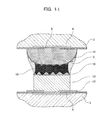
- FIG. 1 is a cross-sectional view for explaining a mounting structure according to a first embodiment.
- the inner layer of a semiconductor chip 1 has a multiple-wiring layer that faces a circuit board 2 .
- the multiple-wiring layer includes a fine wiring layer (not shown) made of materials such as Cu (copper) and Al (aluminum) and a fragile low-dielectric constant insulating layer (an example of an interlayer insulating film) 3 , e.g., a low-k layer or an ultra low-k layer.
- a plurality of electrode terminals (electrode pads) 4 are disposed over the entire area of the outermost surface of the multiple-wiring layer.
- the low-dielectric constant insulating layer 3 has a thickness of several hundreds of nm per layer.
- the electrode terminals 4 of the semiconductor chip 1 are composed of, for example, aluminum alloys such as Al—Cu, Al—Si—Cu, and Al—Si alloys, Cu, and Al.
- Al is selected as a material of the electrode terminals 4 .
- the circuit board 2 has electrode terminals (electrodes pads) 5 that are opposed to the electrode terminals 4 of the semiconductor chip 1 .
- the circuit board 2 may be made of a base material, for example, silicon, polysilicon, or glass.
- the electrode terminals 5 of the circuit board 2 are composed of, for example, aluminum alloys such as Al—Cu, Al—Si—Cu, and Al—Si alloys, Cu, and Al.
- Al is selected as a material of the electrode terminals 5 .
- a protruding electrode (bump) 6 that is a dome with a flat portion is provided on each of the electrode terminals 4 of the semiconductor chip 1 .
- the protruding electrode 6 is an example of a shape having a curvature on the edge.
- a protruding electrode 7 that is a dome with a flat portion is provided on each of the electrode terminals 5 of the circuit board 2 .
- the protruding electrode 7 is an example of a shape having a curvature on the edge.
- the electrode terminals 4 of the semiconductor chip 1 and the electrode terminals 5 of the circuit board 2 are electrically and mechanically connected to each other via the protruding electrodes 6 and 7 , which are provided on the electrode terminals 4 and 5 , an alloy layer 8 , and solder 9 that is an example of a metal having a lower modulus of elasticity than the protruding electrodes 6 and 7 and the alloy layer 8 .
- a junction connecting the electrode terminal 4 of the semiconductor chip 1 and the electrode terminal 5 of the circuit board 2 is composed of the protruding electrodes 6 and 7 , the alloy layer 8 , and the solder 9 .
- the protruding electrodes 6 and 7 are composed of, for example, a Ni—P(phosphorus) alloy, a Ni—B(boron) alloy, and Ni. Alternatively, the protruding electrodes 6 and 7 may have a three-layer structure made of, for example, Ni/Pd(palladium)/Au(gold).
- the solder 9 may be, for example, Sn—Ag solder, Sn—Ag—Cu solder, Sn—Zn(zinc) solder, Sn—Zn—Bi(bismuth) solder, Sn—Pb(lead) solder, Sn—Bi solder, Sn—Ag—Bi—In(indium) solder, Sn—In solder, In solder, or Sn solder.
- the alloy layer 8 is made of, for example, Ni 3 Sn 4 , Ni 3 Sn 2 , Ni 3 Sn, and Ni 3 SnP.
- the principal component of the protruding electrodes 6 and 7 is Ni
- the principal component of the solder 9 is Sn
- the alloy layer 8 is composed of a Ni—Sn alloy (nickel-tin alloy), e.g., Ni 3 Sn 4 .
- FIG. 2 is a cross-sectional view for explaining the mounting structure according to the first embodiment. Specifically, FIG. 2 is a cross-sectional view taken along the line A-A of FIG. 1 so as to illustrate the junctions on a plane located between the protruding electrodes 6 on the semiconductor chip 1 and the protruding electrodes 7 on the circuit board 2 .
- the junctions connecting the electrode terminals 4 of the semiconductor chip 1 and the electrode terminals 5 of the circuit board 2 are evenly spaced in a lattice pattern.
- the electrode terminals 4 of the semiconductor chip 1 and the electrode terminals 5 of the circuit board 2 are also evenly spaced in a lattice pattern.
- the semiconductor chip 1 is slightly curved. This is because a thermal stress caused by a difference in modulus of elasticity and a difference in linear expansion coefficient between the semiconductor chip 1 and the circuit board 2 concentrates on the junctions located on the outer periphery of the semiconductor chip 1 . Hence, the junctions located on the outer periphery of the semiconductor chip 1 are stretched, so that as shown in FIG. 2 , the alloy layer 8 in the junctions located on the outer periphery has a smaller cross-sectional area than the alloy layer 8 in the junctions located at other points.
- the alloy layer 8 in the junctions has a small cross-sectional area particularly around the corners of the rectangular outside shape of the semiconductor chip 1 .
- the solder 9 has a small width (not shown) in the junctions on the outer periphery of the semiconductor chip 1 (particularly at the corner portions of the rectangular outside shape of the semiconductor chip 1 ).
- the corners of the semiconductor chip are points that connect two sides or two ends of the outside shape of the semiconductor chip, on the major surface (element surface) of the semiconductor chip in plan view. The two sides or ends form an angle smaller than 180°. For example, if the semiconductor chip has a rectangular outside shape, two sides or two ends form an angle of 90° at the corners of the semiconductor chip.
- the corner portions of the semiconductor chip indicate the portions of the junctions around the corners of the outside shape of the semiconductor chip on the outer periphery of the semiconductor chip.
- the semiconductor chip 1 has a rectangular outside shape of 4 mm ⁇ 4 mm and has a thickness of 0.2 mm.
- the circuit board 2 has a rectangular outside shape of 8 mm ⁇ 8 mm and has a thickness of 0.5 mm.
- the electrode terminals 4 of the semiconductor chip 1 are shaped like circles that are 20 ⁇ m in diameter and are evenly spaced in a lattice pattern with a pitch of 40 ⁇ m between the electrode terminals (a center to center distance of 40 ⁇ m between the adjacent electrode terminals 4 ).
- the electrode terminals 5 of the circuit board 2 are shaped like circles having a diameter of 20 ⁇ m and are evenly spaced in a lattice pattern with a pitch of 40 ⁇ m between the electrode terminals (a center to center distance of 40 ⁇ m between the adjacent electrode terminals 5 ).
- the electrode terminals 4 of the semiconductor chip 1 and the electrode terminals 5 of the circuit board 2 have circular surfaces exposed with a diameter of 10 ⁇ m from the insulating film.
- the electrode terminals 4 and 5 are 1.0 ⁇ m to 2.0 ⁇ m in thickness.
- FIG. 3 is an enlarged cross-sectional view for explaining the mounting structure according to the first embodiment.
- the alloy layer 8 is formed on the surface of the protruding electrode 6 provided on the electrode terminal 4 of the semiconductor chip 1 .
- the alloy layer 8 is also formed on the surface of the protruding electrode 7 provided on the electrode terminal 5 of the circuit board 2 .
- the surfaces of the protruding electrodes 6 and the protruding electrodes 7 are joined to the solder 9 via the alloy layer 8 .
- the alloy layer 8 grown from the protruding electrode 6 on the semiconductor chip 1 and the alloy layer 8 grown from the protruding electrode 7 on the circuit board 2 are electrically and mechanically connected to each other.
- the alloy layer 8 connecting the protruding electrode 6 on the semiconductor chip 1 and the protruding electrode 7 on the circuit board 2 is also joined to the solder 9 surrounding the alloy layer 8 .
- the alloy layer 8 has a minimum thickness of 0.1 ⁇ m and a maximum thickness of 6.0 ⁇ m at the junction connecting the protruding electrode 6 on the semiconductor chip 1 and the protruding electrode 7 of the circuit board 2 .
- the alloy layer 8 has a thickness of 0.1 ⁇ m to 6.0 ⁇ m.
- FIGS. 4A and 4B are enlarged cross-sectional views for explaining the mounting structure according to the first embodiment.
- FIG. 4A is a cross-sectional view taken along the line B-B of FIG. 3 .
- FIG. 4A shows the junction cut along a plane near the circuit board 2 .
- FIG. 4B is a cross-sectional view taken along the line C-C of FIG. 3 .
- FIG. 4B shows the junction cut along a plane located between the protruding electrode 6 on the semiconductor chip 1 and the protruding electrode 7 on the circuit board 2 .
- the ring-shaped solder 9 is disposed around the circular protruding electrode 7 while the alloy layer 8 is formed between the protruding electrode 7 and the solder 9 .
- the solder 9 contains multiple spots of the alloy layer 8 .
- the junction has a cross section structure including the alloy layer 8 surrounded by the solder 9 that is an example of a metal having a lower modulus of elasticity than the alloy layer 8 .
- the alloy layer 8 is formed by growing multiple shell-like alloys formed on the surfaces of the protruding electrodes 6 and 7 .
- the alloy layer 8 has fine irregularities on the surface.
- FIG. 5 is a flowchart showing the manufacturing method for the mounting structure according to the first embodiment.
- FIGS. 6A to 6I are process cross-sectional views for explaining the manufacturing method for the mounting structure according to the first embodiment.
- the protruding electrode 6 that is a dome with a flat portion is formed on the electrode terminal 4 of the semiconductor chip 1 by electroless plating (step a 1 in FIG. 5 ).
- the protruding electrode 6 is an example of a shape having a curvature on the edge.
- impurities are first removed from the surface of the electrode terminal 4 made of Al.
- the semiconductor chip 1 is immersed into a zinc plating solution so as to undergo a substitution reaction between Al and Zn of the electrode terminal 4 .
- Zn nuclei are removed from the electrode terminal 4 .
- the semiconductor chip 1 is then immersed into the zinc plating solution again.
- the semiconductor chip 1 is immersed into a Ni—P plating solution, so that Zn dissolves and a Ni—P coating is grown on Al of the electrode terminal 4 .
- the semiconductor chip 1 is then immersed into an electroless gold plating solution.
- a Au coating is grown on Ni—P.
- the protruding electrode 6 is 10 ⁇ m in height and the bottom of the protruding electrode 6 is 30 ⁇ m in diameter.
- solder powder 9 a is supplied to the surface of the protruding electrode 6 of the semiconductor chip 1 (step a 2 in FIG. 5 ).
- the solder powder 9 a may be transferred to the surface of the protruding electrode 6 of the semiconductor chip 1 as follows: for example, a solder transfer sheet including an adhesive layer formed on a transfer base is stacked on the heated semiconductor chip 1 such that the adhesive layer with evenly applied fine solder powder or solder particles is opposed to the protruding electrode 6 , and the semiconductor chip 1 is pressed to the solder transfer sheet. At this point, Ni atoms (not shown) of the protruding electrode 6 are diffused into the solder powder 9 a , forming multiple shell-shaped portions of the alloy layer 8 on the interface between the protruding electrode 6 and the solder powder 9 a .
- the alloy layer 8 is composed of, for example, Ni—Sn alloys such as Ni 3 Sn 4 .
- solder powder 9 a may be bonded to the surface of the protruding electrode 6 of the semiconductor chip 1 as follows: for example, after the semiconductor chip 1 is immersed into a tackifier compound composed of a naphthotriazole dielectric, a benzotriazole dielectric, and so on, the semiconductor chip 1 is sprinkled with fine solder powder or solder particles and then is cleaned.
- the semiconductor chip 1 After the step of bonding the solder powder 9 a to the surface of the protruding electrode 6 , the semiconductor chip 1 is heated in a reflow furnace at least to a solder melting point. Thus, the liquid solder powder 9 a is melted so as to be continuously supplied by the surface tension (step a 3 in FIG. 5 ). Hence, as shown in FIG. 6D , the protruding electrode 6 on the semiconductor chip 1 is precoated like a dome with the solder 9 . At this point, in the process of melting solder, Ni atoms contained in the protruding electrode 6 are diffused into molten solder, and the shell-shaped alloy layer 8 is grown on the interface between the protruding electrode 6 and the solder 9 .
- flux may be used to remove an oxide film on a solder surface.
- the solder 9 may be melted by applying flux to the semiconductor chip 1 and then heating the semiconductor chip 1 at least to the melting point of solder in, for example, an atmosphere of inert gas of N 2 in a N 2 reflow furnace.
- a cleaning fluid e.g., isopropyl alcohol (IPA), ethanol, glycol, and a surface-active agent.
- the semiconductor chip 1 may be heated in a reducing atmosphere of, for example, formic acid or hydrogen by using a reflow furnace for reduction instead of flux.
- the circuit board 2 undergoes the same processing as the semiconductor chip 1 .
- the protruding electrode 7 that is a dome with a flat portion is formed on each of the electrode terminals 5 of the circuit board 2 by electroless plating (step b 1 in FIG. 5 ).
- the protruding electrode 7 is an example of a shape having a curvature on the edge.
- the solder powder 9 a is fed onto the protruding electrode 7 (step b 2 in FIG. 5 ).
- the circuit board 2 is then heated at least to the melting point of solder, thereby melting the solder powder 9 a (step b 3 in FIG. 5 ).
- the protruding electrodes 7 are precoated with the solder 9 into domes.
- multiple shell-shaped portions of the alloy layer 8 are formed and grown on the interface between the protruding electrode 7 and the solder 9 .
- the alloy layer 8 is composed of, for example, Ni—Sn alloys such as Ni 3 Sn 4 .
- the protruding electrode 7 is 10 m in height and the bottom of the protruding electrode 7 is 30 ⁇ m in diameter.
- the electrode terminal 4 of the semiconductor chip 1 is aligned with the electrode terminal 5 of the circuit board 2 , and then the semiconductor chip 1 is pressed and mounted onto the circuit board 2 while being heated with the circuit board 2 (step c 1 in FIG. 5 ).
- the semiconductor chip 1 and the circuit board 2 are first heated in an atmosphere of inert gas such as N2 so as to heat the solder 9 on the semiconductor chip 1 and the circuit board 2 at least to the melting point of solder (e.g., 220° C. to 260° C.).
- the solder 9 melts and the alloy layer 8 having fine irregularities starts growing on the surfaces of the protruding electrodes 6 and 7 .
- the semiconductor chip 1 is then pressed onto the circuit board 2 with the molten solder 9 on the semiconductor chip 1 and the circuit board 2 . This mixes the molten solder 9 on the semiconductor chip 1 and the molten solder 9 on the circuit board 2 .
- the semiconductor chip 1 is kept pressed to the circuit board 2 for a certain period of time.
- the semiconductor chip 1 and the circuit board 2 are then cooled at least to the solidifying point of solder.
- the solidification forms the junctions connecting the electrode terminals 4 of the semiconductor chip 1 and the electrode terminals 5 of the circuit board 2 .
- the semiconductor chip 1 and the circuit board 2 are further cooled to room temperature. Hence, the mounting structure is obtained.
- step c 1 in FIG. 5 Ni atoms contained in the protruding electrodes 6 and 7 are diffused during the melting of solder, thereby growing the alloy layer 8 on both of the protruding electrodes 6 and 7 .
- the alloy layer 8 grows on both of the protruding electrodes 6 and 7 so as to connect the protruding electrodes 6 and 7 .
- the semiconductor chip 1 is kept pressed onto the circuit board 2 until the connecting portion of the alloy layers 8 is surrounded by the solder 9 .
- the manufacturing method for the mounting structure according to the first embodiment includes: growing the alloy layer 8 composed of a metal (nickel) constituting the protruding electrode 6 and a metal (tin) constituting the solder 9 and the alloy layer 8 composed of a metal (nickel) constituting the protruding electrode 7 and the metal (tin) constituting the solder 9 , by melting the solder 9 that joins the protruding electrode 6 having a curvature on the edge on the electrode terminal 4 and the protruding electrode 7 having a curvature on the edge on the electrode terminal 5 ; and cooling the molten solder 9 so as to form the junction that connects the electrode terminal 4 and the electrode terminal 5 , the junction having a cross section structure including the alloy layer 8 surrounded by the solder 9 having a lower modulus of elasticity than the alloy layer 8 .
- the protruding electrodes 6 and 7 and the alloy layer 8 are surrounded by the molten solder 9 having a lower modulus of elasticity than the protruding electrodes 6 and 7 and the alloy layer 8 .
- the protruding electrodes 6 and 7 and the alloy layer 8 are surrounded by the solidified solder 9 having a lower modulus of elasticity than the protruding electrodes 6 and 7 and the alloy layer 8 .
- the protruding electrodes 6 and 7 predominantly composed of Ni and the alloy layer 8 composed of a Ni—Sn alloy have a modulus of elasticity of 50 GPa to 60 GPa, whereas the solder 9 predominantly composed of Sn has a low modulus of elasticity of 20 GPa to 40 GPa.
- the junction connecting the electrode terminals 4 and 5 has a modulus of elasticity of, for example, 25 GPa to 45 GPa.
- the semiconductor chip 1 and the circuit board 2 have different elastic moduli and linear expansion coefficients. This reduces a tensile stress applied to the electrode terminal 4 of the semiconductor chip 1 because the junction connecting the electrode terminals 4 and 5 has a lower modulus of elasticity than the protruding electrodes 6 and 7 and the alloy layer 8 .
- a tensile stress applied to the electrode terminal 4 of the semiconductor chip 1 is reduced, a tensile stress applied to the low-dielectric constant insulating layer 3 located immediately under the electrode terminal 4 of the semiconductor chip 1 falls below the destructive strength of the low-dielectric constant insulating layer 3 . This prevents exfoliation and a crack on the fragile low-dielectric constant insulating layer 3 immediately under the electrode terminal 4 of the semiconductor chip 1 , achieving the mounting structure with high connection reliability.
- the protruding electrodes 6 and 7 in particular, have curvatures on the edges, and thus even if the solder 9 contained in the junctions on the outer periphery of the semiconductor chip 1 is extended by a thermal stress caused by a difference in modulus of elasticity and a difference in linear expansion coefficient between the semiconductor chip 1 and the circuit board 2 in the process of cooling the molten solder 9 , the solder 9 does not considerably increase the areas of the exposed surfaces of the protruding electrodes 6 and 7 included in the junctions disposed on the outer periphery of the semiconductor chip 1 . Therefore, the first embodiment prevents exfoliation and a crack on the fragile low-dielectric constant insulating layer 3 on the outer periphery of the semiconductor chip 1 , achieving the mounting structure with high connection reliability.
- the junction connecting the electrode terminal 4 of the semiconductor chip 1 and the electrode terminal 5 of the circuit board 2 includes the cross section structure including the protruding electrodes 6 and 7 and the alloy layer 8 surrounded by the solder 9 that is an example of a metal having a lower modulus of elasticity than the protruding electrodes 6 and 7 and the alloy layer 8 .
- the protruding electrode 6 on the electrode terminal 4 and the protruding electrode 7 on the electrode terminal 5 are connected to each other via the alloy layer 8 , suppressing migration of Ni atoms contained in the protruding electrodes 6 and 7 and Sn atoms contained in the solder 9 , the migration being caused by an electromigration phenomenon. This suppresses the growth of the alloy layer 8 . In other words, the alloy layer 8 is stabilized.
- the mounting structure according to the first embodiment can maintain stable bonding between the electrode terminals 4 and 5 and reduce fluctuations in connection resistance between the electrode terminals 4 and 5 .
- a clearance between the semiconductor chip 1 and the circuit board 2 may be filled with molding resin (not shown) by a dispenser.
- the molding resin further reduces a stress applied to the electrode terminal 4 of the semiconductor chip 1 , further improving connection reliability between the electrode terminal 4 of the semiconductor chip 1 and the electrode terminal 5 of the circuit board 2 .
- the alloy layers 8 grown from the surfaces of the protruding electrodes 6 and 7 may not be connected to each other so as to locate only the solder 9 between the alloy layers 8 .
- the alloy layers 8 may be connected by, for example, heating the solidified solder 9 with a heating device such as a N 2 reflow furnace and a reflow furnace for reduction, and then remelting the solder 9 so as to further grow the alloy layers 8 .
- the alloy layers 8 grown from the surfaces of the protruding electrodes 6 and 7 are connected to each other in the process of continuously pressing the semiconductor chip 1 to the circuit board 2 for a certain period of time, the alloy layers 8 may be further grown by heating the solidified solder 9 and then remelting the solder 9 . This can further stabilize the alloy layer 8 so as to keep the stable connection between the electrode terminals 4 and 5 and reduce fluctuations in connection resistance between the electrode terminals 4 and 5 .
- a large current may be applied between the electrode terminals 4 and 5 so as to further grow the alloy layers 8 by an electromigration phenomenon. This can further stabilize the alloy layer 8 so as to keep the stable connection between the electrode terminals 4 and 5 and reduce fluctuations in connection resistance between the electrode terminals 4 and 5 .
- the first embodiment can obtain high connection reliability even if the pitches between the electrode terminals are reduced in the mounting structure where the electrode terminals of the semiconductor chip and the electrode terminals of the circuit board are electrically and mechanically connected to each other via the fine solder junctions.
- the second embodiment is different from the first embodiment in that the protruding electrodes 7 are replaced with flat electrodes on electrode terminals 5 of a circuit board 2 .
- FIG. 7 is an enlarged cross-sectional view for explaining a mounting structure according to the second embodiment.
- Al is selected as the materials of electrode terminals 4 of a semiconductor chip 1 and the electrode terminals 5 of the circuit board 2 as in the first embodiment.
- the main component of protruding electrodes 6 on the semiconductor chip 1 is Ni
- the main component of solder 9 is Sn
- an alloy layer 8 is composed of Ni—Sn alloys such as Ni 3 Sn 4 .
- the semiconductor chip 1 has a rectangular outside shape of 4 mm ⁇ 4 mm and has a thickness of 0.2 mm.
- the circuit board 2 has a rectangular outside shape of 8 mm ⁇ 8 mm and has a thickness of 0.5 mm.
- the electrode terminals 4 of the semiconductor chip 1 and the electrode terminals 5 of the circuit board 2 are shaped like circles that are 25 ⁇ m in diameter and are evenly spaced in a lattice pattern with a pitch of 50 ⁇ m between the electrode terminals.
- the electrode terminals 4 of the semiconductor chip 1 and the electrode terminals 5 of the circuit board 2 have circular surfaces exposed with a diameter of 15 ⁇ m from an insulating film.
- the electrode terminals 4 and 5 are 1.0 ⁇ m in thickness.
- a barrier metal electrode 10 is formed as an example of a flat electrode on the electrode terminal 5 of the circuit board 2 .
- the barrier metal electrode 10 is circular in plan view and is predominantly composed of Ni.
- the electrode terminals 4 of the semiconductor chip 1 and the electrode terminals 5 of the circuit board 2 are electrically and mechanically connected to each other via the protruding electrodes 6 provided on the electrode terminals 4 of the semiconductor chip 1 , the barrier metal electrodes 10 provided on the electrode terminals 5 of the circuit board 2 , the alloy layer 8 , and the solder 9 that is an example of a metal having a lower modulus of elasticity than the protruding electrodes 6 , the barrier metal electrodes 10 , and the alloy layer 8 .
- the protruding electrode 6 is an example of a shape having a curvature on the edge and is shaped like a dome with a flat portion.
- a junction connecting the electrode terminal 4 of the semiconductor chip 1 and the electrode terminal 5 of the circuit board 2 is composed of the protruding electrode 6 , the barrier metal electrode 10 , the alloy layer 8 , and the solder 9 .
- the alloy layer 8 is formed on the surfaces of the protruding electrode 6 provided on the electrode terminal 4 of the semiconductor chip 1 and the barrier metal electrode 10 provided on the electrode terminal 5 of the circuit board 2 .
- the surfaces of the protruding electrode 6 and the barrier metal electrode 10 are joined to the solder 9 via the alloy layer 8 .
- the alloy layer 8 grown from the protruding electrode 6 on the semiconductor chip 1 and the alloy layer 8 grown from the barrier metal electrode 10 of the circuit board 2 are electrically and mechanically connected to each other.
- the alloy layer 8 connecting the protruding electrode 6 on the semiconductor chip 1 and the barrier metal electrode 10 of the circuit board 2 is also joined to the solder 9 surrounding the alloy layer 8 .
- the alloy layer 8 has a minimum thickness of 0.1 ⁇ m and a maximum thickness of 6.0 ⁇ m at the junction connecting the protruding electrode 6 on the semiconductor chip 1 and the barrier metal electrode 10 of the circuit board 2 .
- the alloy layer 8 has a thickness of 0.1 ⁇ m to 6.0 ⁇ m.
- FIG. 8 is an enlarged cross-sectional view for explaining the mounting structure according to the second embodiment. Specifically, FIG. 8 is a cross-sectional view taken along the line D-D of FIG. 7 . FIG. 8 shows the junction cut along a plane located between the protruding electrode 6 on the semiconductor chip 1 and the barrier metal electrode 10 of the circuit board 2 .
- the solder 9 contains multiple portions of the alloy layer 8 at a position where the alloy layers 8 grown from the protruding electrode 6 and the barrier metal electrode 10 are connected to each other.
- the junction has a cross section structure including the alloy layer 8 surrounded by the solder 9 that is an example of a metal having a lower modulus of elasticity than the alloy layer 8 .
- FIG. 9 is a flowchart showing the manufacturing method for the mounting structure according to the second embodiment.
- FIGS. 10A to 10G are process cross-sectional views for explaining the manufacturing method for the mounting structure according to the second embodiment.
- the protruding electrode 6 that is a dome with a flat portion is formed on the electrode terminal 4 of the semiconductor chip 1 by electroless plating (step a 1 in FIG. 9 ) as in the first embodiment.
- the protruding electrode 6 is an example of a shape having a curvature on the edge.
- the protruding electrode 6 is 10 ⁇ m in height and the bottom of the protruding electrode 6 is 30 ⁇ m in diameter.
- the barrier metal electrode 10 is formed on the electrode terminal 5 of the circuit board 2 (step b 11 in FIG. 9 ). Specifically, a seed layer 11 made of, for example, Ti(titanium)/W(tungsten)/Cu is first formed on the electrode terminal 5 of the circuit board 2 by sputtering. After that, a barrier metal layer made of, for example, Ni is formed thereon by electrolytic plating. The unnecessary seed layer 11 and the unnecessary barrier metal layer are then removed by photolithography. Thus, the barrier metal electrode 10 is formed. In the second embodiment, the barrier metal electrode 10 is 25 ⁇ m in diameter and is 2.0 ⁇ m to 5.0 ⁇ m in thickness.
- the solder 9 is fed onto the barrier metal electrode 10 (step b 12 in FIG. 9 ). Specifically, a resist film 12 having a thickness of 10 ⁇ m to 15 ⁇ m is formed on a plane where the electrode terminal 5 of the circuit board 2 is disposed, and then an opening that exposes the barrier metal electrode 10 is formed on the resist film 12 . After that, the circuit board 2 is immersed into a solder plating solution so as to feed the solder 9 into the opening of the resist film 12 .
- the circuit board 2 is heated in a reflow furnace at least to the melting point of solder, thereby melting the solder 9 (step b 13 in FIG. 9 ).
- the solder 9 on the barrier metal electrode 10 is shaped like a part of a sphere.
- a solder bump is formed on the barrier metal electrode 10 .
- Ni atoms contained in the barrier metal electrode 10 are diffused into the solder so as to form multiple shell-shaped portions of the alloy layer 8 on the interface between the barrier metal electrode 10 and the solder 9 .
- the alloy layer 8 is composed of, for example, Ni—Sn alloys such as Ni 3 Sn 4 .
- the solder bump has a height of 10 ⁇ m to 15 ⁇ m and a maximum diameter of 30 ⁇ m.
- flux may be used to remove an oxide film on a solder surface.
- the solder 9 may be melted by applying flux to the circuit board 2 and then heating the circuit board 2 at least to the melting point of solder in, for example, an atmosphere of inert gas of N 2 in a N 2 reflow furnace.
- a cleaning fluid e.g., isopropyl alcohol (IPA), ethanol, glycol, and a surface-active agent.
- the circuit board 2 may be heated in a reducing atmosphere of, for example, formic acid or hydrogen by using a reflow furnace for reduction instead of flux.
- the electrode terminals 4 of the semiconductor chip 1 are aligned with the electrode terminals 5 of the circuit board 2 , and then the semiconductor chip 1 is pressed and mounted onto the circuit board 2 while being heated with the circuit board 2 in, for example, an atmosphere of inert gas of N 2 (step d 1 in FIG. 9 ).
- the solder 9 is first heated at least to the melting point of solder (e.g., 220° C. to 260° C.) and thus the solder 9 melts.
- the alloy layer 8 starts growing on the surfaces of the barrier metal electrodes 10 of the circuit board 2 .
- the semiconductor chip 1 is then pressed to the circuit board 2 with the molten solder 9 .
- a diffusion reaction starts between the molten solder 9 and the protruding electrode 6 on the semiconductor chip 1 , forming multiple shell-shaped portions of the alloy layer 8 on the interface between the protruding electrode 6 and the solder 9 .
- the semiconductor chip 1 is kept pressed to the circuit board 2 for a certain period of time.
- the semiconductor chip 1 and the circuit board 2 are then cooled at least to the solidifying point of solder.
- the solidification forms the junctions connecting the electrode terminals 4 of the semiconductor chip 1 and the electrode terminals 5 of the circuit board 2 .
- the semiconductor chip 1 and the circuit board 2 are further cooled to room temperature. Hence, the mounting structure is obtained.
- step c 11 in FIG. 9 Ni atoms contained in the barrier metal electrode 10 of the circuit board 2 and the protruding electrode 6 on the semiconductor chip 1 are diffused during the melting of solder, thereby growing the alloy layer 8 on both of the barrier metal electrode 10 and the protruding electrode 6 .
- the alloy layer 8 grows on both of the barrier metal electrode 10 and the protruding electrode 6 so as to connect the barrier metal electrode 10 and the protruding electrode 6 .
- the semiconductor chip 1 is kept pressed onto the circuit board 2 until the connecting portion of the alloy layers 8 is surrounded by the solder 9 .
- the manufacturing method for the mounting structure according to the second embodiment includes: growing the alloy layer 8 composed of a metal (nickel) constituting the protruding electrode 6 and a metal (tin) constituting the solder 9 and the alloy layer 8 composed of a metal (nickel) constituting the barrier metal electrode 10 and the metal (tin) constituting the solder 9 , by melting the solder 9 that joins the protruding electrode 6 having a curvature on the edge on the electrode terminal 4 and the barrier metal electrode 10 that is an example of an flat electrode provided on the electrode terminal 5 ; and cooling the solder 9 so as to form the junction that connects the electrode terminal 4 and the electrode terminal 5 , the junction having a cross section structure including the alloy layer surrounded by the solder 9 having a lower modulus of elasticity than the alloy layer 8 .
- the protruding electrodes 7 are replaced with the flat electrodes on the electrode terminals 5 of the circuit board 2 .
- the content of solder in the junction connecting the electrode terminal 4 of the semiconductor chip 1 and the electrode terminal 5 of the circuit board 2 that is, the content of Sn is larger than in the first embodiment. This can reduce the modulus of elasticity of the junction more than in the first embodiment.
- a fragile low-dielectric constant insulating layer 3 immediately under the electrode terminal 4 of the semiconductor chip 1 is an extremely low-k layer that is more fragile than an ultra low-k layer, exfoliation and a crack can be prevented on the low-dielectric constant insulating layer 3 , achieving the mounting structure with higher connection reliability.
- the third embodiment is different from the first embodiment in that the protruding electrodes 7 are replaced with cylindrical electrodes on electrode terminals 5 of a circuit board 2 .
- the cylindrical electrodes are made of a metal having a lower modulus of elasticity than protruding electrodes 6 on a semiconductor chip 1 .
- FIG. 11 is an enlarged cross-sectional view for explaining a mounting structure according to the second embodiment.
- Al is selected as the materials of electrode terminals 4 of the semiconductor chip 1 and the electrode terminals 5 of the circuit board 2 as in the first embodiment.
- the main component of the protruding electrodes 6 on the semiconductor chip 1 is Ni and the main component of solder 9 is Sn.
- the semiconductor chip 1 has a rectangular outside shape of 4 mm ⁇ 4 mm and has a thickness of 0.2 mm.
- the circuit board 2 has a rectangular outside shape of 8 mm ⁇ 8 mm and has a thickness of 0.5 mm.
- the electrode terminals 4 of the semiconductor chip 1 and the electrode terminals 5 of the circuit board 2 are shaped like circles that are 20 ⁇ m in diameter and are evenly spaced in a lattice pattern with a pitch of 40 ⁇ m between the electrode terminals.
- the electrode terminals 4 of the semiconductor chip 1 and the electrode terminals 5 of the circuit board 2 have circular surfaces exposed with a diameter of 10 ⁇ m from an insulating film.
- the electrode terminals 4 and 5 are 1.0 ⁇ m to 2.0 ⁇ m in thickness.
- a cylindrical electrode 13 predominantly composed of Cu is formed as an example of a cylindrical electrode on the electrode terminal 5 of the circuit board 2 .
- the electrode terminals 4 of the semiconductor chip 1 and the electrode terminals 5 of the circuit board 2 are electrically and mechanically connected to each other via the protruding electrodes 6 provided on the electrode terminals 4 of the semiconductor chip 1 , the cylindrical electrodes 13 provided on the electrode terminals 5 of the circuit board 2 , first to third alloy layers 14 to 16 , and the solder 9 that is an example of a metal having a lower modulus of elasticity than the protruding electrodes 6 , the cylindrical electrodes 13 , and the alloy layers 14 to 16 .
- the protruding electrode 6 is an example of a shape having a curvature on the edge and is shaped like a dome with a flat portion.
- a junction connecting the electrode terminal 4 of the semiconductor chip 1 and the electrode terminal 5 of the circuit board 2 is composed of the protruding electrode 6 , the cylindrical electrode 13 , the first to third alloy layers 14 to 16 , and the solder 9 .
- the first alloy layer 14 is formed on the surface of the protruding electrode 6 provided on the electrode terminal 4 of the semiconductor chip 1 while the second alloy layer 15 is formed on the top of the cylindrical electrode 13 provided on the electrode terminal 5 of the circuit board 2 .
- the first alloy layer 14 and the second alloy layer 15 are electrically and mechanically connected to each other via the solder 9 and the third alloy layer 16 .
- the third alloy layer 16 interposed between the protruding electrode 6 on the semiconductor chip 1 and the cylindrical electrode 13 on the circuit board 2 is also joined to the solder 9 that surrounds the third alloy layer 16 .
- the first alloy layer 14 is grown to have a thickness of 1 ⁇ m to 5 ⁇ m.
- the second alloy layer 15 and the third alloy layer 16 are grown to have a thickness of 2 ⁇ m to 10 ⁇ m.
- the first alloy layer 14 grown from the protruding electrode 6 on the semiconductor chip 1 is composed of alloys such as Ni 3 Sn 4 , Ni 3 Sn 2 , Ni 3 Sn, and Ni 3 SnP.
- the first alloy layer 14 is composed of a Ni—Sn alloy such as Ni 3 Sn 4 will be described.
- the first alloy layer 14 will be referred to as a Ni—Sn (nickel-tin) alloy layer 14 .
- the second alloy layer 15 grown from the cylindrical electrode 13 on the circuit board 2 is composed of Sn—Cu alloys such as Cu 3 Sn and Cu 6 Sn
- the third alloy layer 16 grown on the interface between the first alloy layer 14 and the second alloy layer 15 is composed of Ni—Sn—Cu alloys such as (Cu, Ni) 6 Sn 5 and (Ni, Cu) 3 Sn 2
- the second alloy layer 15 will be referred to as a Sn—Cu (tin-copper) alloy layer 15
- the third alloy layer 16 will be referred to as a Ni—Sn—Cu (nickel-tin-copper) alloy layer 16 .
- the solder 9 contains multiple portions (not shown) of the Ni—Sn alloy layer 14 , the Sn—Cu alloy layer 15 , and the Ni—Sn—Cu alloy layer 16 .
- the junction connecting the electrode terminal 4 of the semiconductor chip 1 and the electrode terminal 5 of the circuit board 2 has a cross section structure in which the Ni—Sn alloy layer 14 , the Sn—Cu alloy layer 15 , and the Ni—Sn—Cu alloy layer 16 are surrounded by the solder 9 that is an example of a metal having a lower modulus of elasticity than the Ni—Sn alloy layer 14 , the Sn—Cu alloy layer 15 , and the Ni—Sn—Cu alloy layer 16 .
- FIG. 12 is a flowchart showing the manufacturing method for the mounting structure according to the third embodiment.
- FIGS. 13A to 13G are process cross-sectional views for explaining the manufacturing method for the mounting structure according to the third embodiment.
- the protruding electrode 6 that is a dome with a flat portion is formed on the electrode terminal 4 of the semiconductor chip 1 by electroless plating (step a 1 in FIG. 12 ) as in the first embodiment.
- the protruding electrode 6 is an example of a shape having a curvature on the edge.
- solder powder 9 a is fed onto the protruding electrode 6 (step a 2 in FIG. 12 ).
- the semiconductor chip 1 is then heated at least to the melting point of solder, thereby melting the solder powder 9 a (step a 3 in FIG. 12 ).
- the protruding electrodes 6 are precoated with the solder 9 into domes.
- multiple shell-shaped portions of the Ni—Sn alloy layer 14 are formed and grown on the interface between the protruding electrode 6 and the solder 9 .
- the protruding electrode 6 is 10 ⁇ m in height and the bottom of the protruding electrode 6 is 30 ⁇ m in diameter.
- the cylindrical electrode 13 is formed on the electrode terminal 5 of the circuit board 2 by sputtering, electrolytic plating, and photolithography such that the top of the electrode 13 is covered with the solder 9 (step b 21 in FIG. 12 ).
- a seed layer 17 made of, for example, Ti/W/Cu is formed on the electrode terminal 5 of the circuit board 2 by sputtering.
- Cu is deposited on the seed layer 17 by electrolytic plating, and then solder is deposited on Cu by electrolytic plating.
- the unnecessary seed layer 17 , Cu, and solder are removed by photolithography.
- the cylindrical electrode 13 is formed with the top covered with the solder 9 .
- the cylindrical electrode 13 is 10 ⁇ m to 15 ⁇ m in height and is 18 ⁇ m to 22 ⁇ m in diameter.
- the electrode terminals 4 of the semiconductor chip 1 are aligned with the electrode terminals 5 of the circuit board 2 , and then the semiconductor chip 1 is pressed and mounted onto the circuit board 2 while being heated with the circuit board 2 (step c 21 in FIG. 12 ).
- the semiconductor chip 1 and the circuit board 2 are first heated in, for example, an atmosphere of inert gas of N 2 so as to heat the solder 9 provided on the semiconductor chip 1 and the circuit board 2 at least to the melting point of solder (e.g., 220° C. to 260° C.) Thus, the solder 9 melts.
- the Ni—Sn alloy layer 14 at this point starts growing on the surfaces of the protruding electrodes 6 on the semiconductor chip 1 .
- the semiconductor chip 1 is pressed to the circuit board 2 with the molten solder 9 on the semiconductor chip 1 and the molten solder 9 on the circuit board 2 .
- Cu atoms contained in the cylindrical electrodes 13 on the circuit board 2 are diffused into the molten solder, forming multiple shell-shaped portions of the Sn—Cu alloy layer 15 on the interfaces between the cylindrical electrodes 13 and the solder 9 .
- the semiconductor chip 1 and the circuit board 2 are then cooled at least to the solidifying point of solder, thereby solidifying the solder 9 . After that, the semiconductor chip 1 and the circuit board 2 are further cooled to room temperature so as to obtain the mounting structure.
- the mounting structure that does not apply a load to the semiconductor chip 1 and the circuit board 2 is heated by a heating device, for example, a N 2 reflow furnace or a reflow furnace for reduction.
- a heating device for example, a N 2 reflow furnace or a reflow furnace for reduction.
- the mounting structure is reheated at least to the melting point of solder and then the temperature is kept for a certain period of time.
- the Sn—Cu alloy layer 15 grows from the cylindrical electrode 13 ; meanwhile, the Ni—Sn alloy layer 14 on the protruding electrode 6 further grows.
- the Sn—Cu alloy layer 15 then reaches the Ni—Sn alloy layer 14 , forming the Ni—Sn—Cu alloy layer 16 on the interface between the Ni—Sn alloy layer 14 and the Sn—Cu alloy layer 15 .
- the Ni—Sn alloy layer 14 grown from the protruding electrode 6 and the Sn—Cu alloy layer 15 grown from the cylindrical electrode 13 are connected to each other, and then the Ni—Sn—Cu alloy layer 16 is grown from the interface between the alloy layers 14 and 15 .
- the mounting structure is kept at the melting point of solder or higher until the Ni—Sn alloy layer 14 , the Sn—Cu alloy layer 15 , and the Ni—Sn—Cu alloy layer 16 are surrounded by the solder 9 that is an example of a metal having a lower modulus of elasticity than the Ni—Sn alloy layer 14 , the Sn—Cu alloy layer 15 , and the Ni—Sn—Cu alloy layer 16 .
- the Ni—Sn—Cu alloy layer 16 is grown until a part of the surface of the protruding electrode 6 and a part of the surface of the cylindrical electrode 13 are electrically and mechanically connected only via the Ni—Sn—Cu alloy layer 16 .
- the mounting structure is cooled at least to the solidifying point of solder. This solidifies the solder 9 so as to form the junction shown in FIG. 13G .
- the mounting structure is then further cooled to room temperature. Thus, the desired mounting structure can be obtained.
- the mounting structure including the semiconductor chip 1 mounted on the circuit board 2 is obtained, the mounting structure is reheated so as to grow the alloy layers 14 , 15 , and 16 in the junction.
- a plurality of mounting structures cooled to room temperature can be simultaneously heated by a heating device, e.g., a N 2 reflow furnace or a reflow furnace for reduction, thereby simultaneously growing the alloy layers 14 , 15 and 16 in the junctions of the mounting structures.
- a heating device e.g., a N 2 reflow furnace or a reflow furnace for reduction, thereby simultaneously growing the alloy layers 14 , 15 and 16 in the junctions of the mounting structures.
- the alloy layers 14 , 15 , and 16 can be also grown by continuous heating.
- the manufacturing method for the mounting structure according to the third embodiment includes: growing the Ni—Sn alloy layer 14 composed of a metal (nickel) constituting the protruding electrode 6 and a metal (tin) constituting the solder 9 , the Sn—Cu alloy layer 15 composed of a metal (copper) constituting the cylindrical electrode 13 and the metal (tin) constituting the solder 9 , and the Ni—Sn—Cu alloy layer 16 composed of the metal (nickel) constituting the protruding electrode 6 , the metal (tin) constituting the solder 9 , and the metal (copper) constituting the cylindrical electrode 13 , by melting the solder 9 that joins the protruding electrode 6 having a curvature on the edge on the electrode terminal 4 and the cylindrical electrode 13 that is an example of a cylindrical electrode provided on the electrode terminal 5 ; and cooling the solder 9 so as to form the junction that connects the electrode terminal 4 and the electrode terminal 5 , the junction having a cross section structure including the Ni—Sn alloy layer 14
- the metal (copper) constituting the cylindrical electrode 13 has a lower modulus of elasticity than the metal (nickel) constituting the protruding electrode 6
- the content of the metal having a lower modulus of elasticity than the metal (nickel) constituting the protruding electrode 6 is larger in the alloy layer of the junction than in the first embodiment.
- the cylindrical electrode 13 is made of the metal (Cu) having a lower modulus of elasticity than the metal (Ni) constituting the protruding electrode 6 , allowing the alloy layer to contain Cu having a lower modulus of elasticity than Ni.
- the fourth embodiment is different from the first embodiment in that at a cross-sectional position having a maximum solder ratio in at least one junction disposed on the outer periphery of a semiconductor chip 1 , the ratio of solder 9 is higher than that at a cross-sectional position having a maximum solder ratio in at least one junction disposed at the center of the semiconductor chip 1 .
- the cross-sectional position having the maximum solder ratio is a cross-sectional position where the ratio of the solder 9 is maximized in the junction.
- FIG. 14A is a cross-sectional view for explaining a mounting structure according to the fourth embodiment.
- the semiconductor chip 1 has a rectangular outside shape.
- the semiconductor chip 1 in the fourth embodiment is smaller in thickness and is more curved than in the first embodiment.
- a distance between protruding electrodes 6 on the semiconductor chip 1 and protruding electrodes 7 on a circuit board 2 increases toward the corners of the semiconductor chip 1 from the center of the semiconductor chip 1 .
- FIG. 14B is a cross-sectional view taken along the line E-E of FIG. 14A .
- FIG. 14B shows the junction cut at the cross-sectional position having the maximum solder ratio at the corner of the semiconductor chip 1 having a rectangular outside shape.
- FIG. 14C is a cross-sectional view taken along the line F-F of FIG. 14A .
- FIG. 14C shows the junction cut at the cross-sectional position having the maximum solder ratio at the center of the semiconductor chip 1 having a rectangular outside shape.
- the ratio of the solder 9 is higher than that at the cross-sectional position having the maximum solder ratio in the junction disposed at the center of the semiconductor chip 1 in the mounting structure of the fourth embodiment.
- the semiconductor chip 1 has a rectangular outside shape of 4 mm ⁇ 4 mm and has a thickness of 0.05 mm.
- the circuit board 2 has a rectangular outside shape of 8 mm ⁇ 8 mm and has a thickness of 0.5 mm.
- Electrode terminals 4 of the semiconductor chip 1 and electrode terminals 5 of the circuit board 2 are shaped like circles having a diameter of 25 ⁇ m and are evenly spaced in a lattice pattern with a pitch of 50 ⁇ m between the electrode terminals.
- the electrode terminals 4 of the semiconductor chip 1 and the electrode terminals 5 of the circuit board 2 have circular surfaces exposed with a diameter of 15 ⁇ m from an insulating film.
- the electrode terminals 4 and 5 are 1.0 ⁇ m in thickness.
- the protruding electrodes 6 are formed on the semiconductor chip 1 and are precoated with the solder 9 into domes.
- the protruding electrodes 7 are formed on the circuit board 2 and are precoated with the solder 9 into domes.
- the semiconductor chip 1 and the circuit board 2 are first heated in, for example, an atmosphere of inert gas of N 2 so as to heat the solder 9 on the semiconductor chip 1 and the circuit board 2 at least to the melting point of solder (e.g., 220° C. to 260° C.)
- the semiconductor chip 1 is then pressed onto the circuit board 2 with the molten solder 9 on the semiconductor chip 1 and the circuit board 2 . This mixes the molten solder 9 on the semiconductor chip 1 and the molten solder 9 on the circuit board 2 .
- the pressing operation is stopped so as to remove pressures against the semiconductor chip 1 and the circuit board 2 .
- the semiconductor chip 1 is more curved than in the first embodiment.
- the junctions located on the outer periphery (at least at the corners) of the semiconductor chip 1 are set higher than that at the center of the semiconductor chip 1 .
- the junctions located on the outer periphery (at least at the corners) of the semiconductor chip 1 are set higher than those of the first embodiment, and differences in height between the junctions located on the outer periphery (at least at the corners) of the semiconductor chip 1 and the junction located at the center of the semiconductor chip 1 are larger than those of the first embodiment.
- the solder 9 included in the junctions located on the outer periphery (at least at the corners) of the semiconductor chip 1 is more extended than in the first embodiment. This causes the junctions located on the outer periphery (at least at the corners) of the semiconductor chip 1 to have a smaller cross-sectional area than the junction located at the center of the semiconductor chip 1 . Consequently, at the cross-sectional positions having the maximum solder ratio in the junctions located on the outer periphery (at least at the corners) of the semiconductor chip 1 , the ratio of solder 9 is higher than that at the cross-sectional position having the maximum solder ratio in the junction disposed at the center of the semiconductor chip 1 .
- the semiconductor chip 1 and the circuit board 2 are then cooled at least to the solidifying point of solder.
- the solidification forms the junctions connecting the electrode terminals 4 of the semiconductor chip 1 and the electrode terminals 5 of the circuit board 2 .
- the semiconductor chip 1 and the circuit board 2 are then cooled at least to room temperature, achieving the mounting structure.
- pressures against the semiconductor chip 1 and the circuit board 2 are reduced in the step of melting the solder 9 such that at the cross-sectional position having the maximum solder ratio in the at least one junction disposed on the outer periphery of the semiconductor chip 1 , the ratio of the solder 9 is higher than that at the cross-sectional position having the maximum solder ratio in the at least one junction disposed at the center of the semiconductor chip 1 .
- the content of Sn having a low modulus of elasticity is higher than that of the first embodiment.
- a tensile stress applied to the electrode terminals 4 of the semiconductor chip 1 can be smaller than in the first embodiment. This can further suppress exfoliation and a crack on a fragile low-dielectric constant insulating layer 3 immediately under the electrode terminals 4 located at the corners of the semiconductor chip 1 , though a tensile stress applied to the layer immediately under the electrode terminals 4 of the semiconductor chip 1 is maximized at the corners of the semiconductor chip 1 by thermal expansion and vibrations.
- the ratio of the solder 9 can be higher than in the second embodiment at the cross-sectional positions having the maximum solder ratio in the junctions disposed on the outer periphery (at least at the corners of the semiconductor chip 1 if the semiconductor chip 1 has a rectangular outside shape) of the semiconductor chip 1 .
- the ratio of the solder 9 can be higher than in the third embodiment at the cross-sectional positions having the maximum solder ratio in the junctions disposed on the outer periphery (at least at the corners of the semiconductor chip 1 if the semiconductor chip 1 has a rectangular outside shape) of the semiconductor chip 1 .
- the fifth embodiment is different from the first embodiment in that in a junction having a larger current value than other junctions per unit time, the content of solder 9 is smaller than those in the other junctions.
- an alloy layer 8 is more grown and stabilized than in the first embodiment, the alloy layer 8 being fed with a large current in the actual use of a semiconductor device including a mounting structure according to the fifth embodiment.
- FIG. 15A is a plan view for explaining the mounting structure according to the fifth embodiment.
- large-current carrying pads 18 and 19 electrically connected to a power supply or the like are disposed around a region containing electrode terminals on a surface of a circuit board 2 containing the electrode terminals 5 .
- the large-current carrying pads 18 and 19 are electrically connected to predetermined electrode terminals 5 a and 5 b of the electrode terminals 5 of the circuit board 2 via wires.
- the large-current carrying pads 18 and 19 are electrically connected to the electrode terminals 5 a and 5 b facing two electrode terminals 4 disposed at the corners of a semiconductor chip 1 having a rectangular outside shape.
- FIG. 15B is a cross-sectional view of the junction on the electrode terminal 5 a electrically connected to the large-current carrying pad 18 .
- the junction is cut along a plane located between a protruding electrode 6 on the semiconductor chip 1 and a protruding electrode 7 on the circuit board 2 .
- FIG. 15C is a cross-sectional view of the junction on an electrode terminal 5 c that is disposed near the electrode terminal 5 a electrically connected to the large-current carrying pad 18 without being electrically connected to the large-current carrying pad 18 or 19 .
- the junction is cut along the plane located between the protruding electrode 6 on the semiconductor chip 1 and the protruding electrode 7 on the circuit board 2 .
- the electrode terminal 5 c also faces the electrode terminal 4 at the corner of the semiconductor chip 1 , out of the electrode terminals 4 of the semiconductor chip 1 having a rectangular outside shape. However, a large current is not applied to the electrode terminal 5 c.
- the alloy layer 8 in the junction on the electrode terminal 5 a electrically connected to the large-current carrying pad 18 has a larger cross-sectional area than the alloy layer 8 in the junction on the electrode terminal 5 c electrically unconnected to the large-current carrying pads 18 and 19 .
- the alloy layer 8 in the junction on the electrode terminal 5 a electrically connected to the large-current carrying pad 18 is more grown and stabilized than the alloy layer 8 in the junction on the electrode terminal 5 c electrically unconnected to the large-current carrying pads 18 and 19 .
- the manufacturing method according to the fifth embodiment is different from the first embodiment in the step of further growing the alloy layer 8 in the junction by applying a large current only to the junction after the step of mounting the semiconductor chip 1 on the circuit board 2 , the large current being applied to the junction in the actual use of the semiconductor device including the mounting structure according to the fifth embodiment.
- the manufacturing method according to the fifth embodiment includes the step of applying a current only to the large-current carrying pads 18 and 19 so as to accelerate the growth of the alloy layer 8 in the junctions on the electrode terminals 5 a and 5 b of the circuit board 2 after the step of mounting the semiconductor chip 1 on the circuit board 2 .
- the fifth embodiment suppresses the migration of Ni atoms contained in the protruding electrodes 6 and 7 on the electrode terminals 5 a and 5 b of the circuit board 2 and Sn atoms contained in the solder 9 on the electrode terminals 5 a and 5 b of the circuit board 2 in the actual use of the semiconductor device, the migration being caused by an electromigration phenomenon.
- This suppresses the growth of the alloy layer 8 .
- the alloy layer 8 is stabilized on the electrode terminals 5 a and 5 b that receive a large current in the actual use of the semiconductor device.
- the mounting structure can be obtained with more stable connection reliability.
- the alloy layer can be grown and stabilized in the junction that receives a large current in the actual use of the semiconductor device.
- the present invention is particularly useful for the field of mounting, on a circuit board, a semiconductor chip having electrode terminals with smaller pitches or a semiconductor chip having an interlayer insulating film made of a low-dielectric constant material.
Landscapes
- Engineering & Computer Science (AREA)
- Computer Hardware Design (AREA)
- Microelectronics & Electronic Packaging (AREA)
- Power Engineering (AREA)
- Mechanical Engineering (AREA)
- Manufacturing & Machinery (AREA)
- Wire Bonding (AREA)
- Electric Connection Of Electric Components To Printed Circuits (AREA)
Applications Claiming Priority (3)
| Application Number | Priority Date | Filing Date | Title |
|---|---|---|---|
| JP2011202496 | 2011-09-16 | ||
| JP2011-202496 | 2011-09-16 | ||
| PCT/JP2012/005026 WO2013038594A1 (ja) | 2011-09-16 | 2012-08-08 | 実装構造およびその製造方法 |
Publications (2)
| Publication Number | Publication Date |
|---|---|
| US20140217595A1 US20140217595A1 (en) | 2014-08-07 |
| US9373595B2 true US9373595B2 (en) | 2016-06-21 |
Family
ID=47882847
Family Applications (1)
| Application Number | Title | Priority Date | Filing Date |
|---|---|---|---|
| US14/342,935 Active US9373595B2 (en) | 2011-09-16 | 2012-08-08 | Mounting structure and manufacturing method for same |
Country Status (6)
| Country | Link |
|---|---|
| US (1) | US9373595B2 (ja) |
| JP (1) | JP5638144B2 (ja) |
| KR (1) | KR101574911B1 (ja) |
| CN (1) | CN103718280B (ja) |
| TW (1) | TWI536521B (ja) |
| WO (1) | WO2013038594A1 (ja) |
Families Citing this family (9)
| Publication number | Priority date | Publication date | Assignee | Title |
|---|---|---|---|---|
| JP6197325B2 (ja) * | 2013-03-27 | 2017-09-20 | 富士通株式会社 | 電子装置の製造方法 |
| US20170365569A1 (en) * | 2013-12-02 | 2017-12-21 | Smartrac Technology Gmbh | Contact Bumps and Methods of Making Contact Bumps on Flexible Electronic Devices |
| JP2015177113A (ja) * | 2014-03-17 | 2015-10-05 | 株式会社東芝 | 半導体装置およびその製造方法 |
| JP6094533B2 (ja) * | 2014-06-09 | 2017-03-15 | トヨタ自動車株式会社 | 半導体装置 |
| KR102311677B1 (ko) | 2014-08-13 | 2021-10-12 | 삼성전자주식회사 | 반도체소자 및 그 제조방법 |
| JP5944979B1 (ja) * | 2014-12-26 | 2016-07-05 | 千住金属工業株式会社 | はんだ転写シート、はんだバンプ及びはんだ転写シートを用いたはんだプリコート方法 |
| JP7259942B2 (ja) * | 2019-03-29 | 2023-04-18 | 株式会社村田製作所 | 樹脂多層基板、および樹脂多層基板の製造方法 |
| EP3806146A1 (en) | 2019-10-11 | 2021-04-14 | Infineon Technologies Austria AG | Semiconductor device with a diffusion soldered joint with precipitates of a further intermetallic compound and a corresponding manufacturing method |
| US11502056B2 (en) * | 2020-07-08 | 2022-11-15 | Taiwan Semiconductor Manufacturing Company, Ltd. | Joint structure in semiconductor package and manufacturing method thereof |
Citations (17)
| Publication number | Priority date | Publication date | Assignee | Title |
|---|---|---|---|---|
| JPH02237129A (ja) | 1989-03-10 | 1990-09-19 | Nippon Steel Corp | 半導体素子接続構造 |
| JPH0997791A (ja) | 1995-09-27 | 1997-04-08 | Internatl Business Mach Corp <Ibm> | バンプ構造、バンプの形成方法、実装接続体 |
| JPH10303548A (ja) | 1997-04-30 | 1998-11-13 | Matsushita Electric Ind Co Ltd | 半導体部品接合方法 |
| JP2002280407A (ja) | 2001-03-21 | 2002-09-27 | Seiko Epson Corp | 半導体チップ及び半導体装置、回路基板並びに電子機器 |
| US6608381B1 (en) | 1994-07-20 | 2003-08-19 | Fujitsu Limited | Integrated electronic device having flip-chip connection with circuit board and fabrication method thereof |
| JP2003282617A (ja) | 2002-03-25 | 2003-10-03 | Citizen Watch Co Ltd | 半導体装置およびその製造方法 |
| US20060017171A1 (en) * | 2004-07-23 | 2006-01-26 | Advanced Semiconductor Engineering Inc. | Formation method and structure of conductive bumps |
| US6995469B2 (en) | 2003-05-21 | 2006-02-07 | Olympus Corporation | Semiconductor apparatus and fabricating method for the same |
| JP2006156492A (ja) | 2004-11-25 | 2006-06-15 | Rohm Co Ltd | 半導体装置 |
| CN101156236A (zh) | 2005-04-06 | 2008-04-02 | 松下电器产业株式会社 | 倒装片安装方法及凸块形成方法 |
| US20080237314A1 (en) * | 2007-03-28 | 2008-10-02 | Jin Yu | Method of joining electronic package capable of prevention for brittle fracture |
| US20080265006A1 (en) * | 2007-04-27 | 2008-10-30 | Jin Yu | Method for bonding electronic components finished with electroless NiXP for preventing brittle fracture |
| US20090297879A1 (en) * | 2008-05-12 | 2009-12-03 | Texas Instruments Incorporated | Structure and Method for Reliable Solder Joints |
| US7772032B2 (en) | 2007-11-28 | 2010-08-10 | Nec Electronics Corporation | Manufacturing method for electronic devices |
| US20110012263A1 (en) | 2009-07-16 | 2011-01-20 | Renesas Electronics Corporation | Semiconductor device and manufacturing method of the same |
| US20110285015A1 (en) * | 2010-05-23 | 2011-11-24 | Nepes Corporation | Bump structure and fabrication method thereof |
| US20140054766A1 (en) * | 2012-07-27 | 2014-02-27 | Nippon Steel & Sumikin Materials Co., Ltd. | Lead-free solder bump bonding structure |
-
2012
- 2012-08-08 CN CN201280038204.3A patent/CN103718280B/zh active Active
- 2012-08-08 WO PCT/JP2012/005026 patent/WO2013038594A1/ja active Application Filing
- 2012-08-08 KR KR1020147002083A patent/KR101574911B1/ko active IP Right Grant
- 2012-08-08 US US14/342,935 patent/US9373595B2/en active Active
- 2012-08-08 JP JP2013533467A patent/JP5638144B2/ja active Active
- 2012-08-31 TW TW101131907A patent/TWI536521B/zh active
Patent Citations (19)
| Publication number | Priority date | Publication date | Assignee | Title |
|---|---|---|---|---|
| JPH02237129A (ja) | 1989-03-10 | 1990-09-19 | Nippon Steel Corp | 半導体素子接続構造 |
| US6608381B1 (en) | 1994-07-20 | 2003-08-19 | Fujitsu Limited | Integrated electronic device having flip-chip connection with circuit board and fabrication method thereof |
| JPH0997791A (ja) | 1995-09-27 | 1997-04-08 | Internatl Business Mach Corp <Ibm> | バンプ構造、バンプの形成方法、実装接続体 |
| JPH10303548A (ja) | 1997-04-30 | 1998-11-13 | Matsushita Electric Ind Co Ltd | 半導体部品接合方法 |
| JP2002280407A (ja) | 2001-03-21 | 2002-09-27 | Seiko Epson Corp | 半導体チップ及び半導体装置、回路基板並びに電子機器 |
| JP2003282617A (ja) | 2002-03-25 | 2003-10-03 | Citizen Watch Co Ltd | 半導体装置およびその製造方法 |
| US6995469B2 (en) | 2003-05-21 | 2006-02-07 | Olympus Corporation | Semiconductor apparatus and fabricating method for the same |
| US20060017171A1 (en) * | 2004-07-23 | 2006-01-26 | Advanced Semiconductor Engineering Inc. | Formation method and structure of conductive bumps |
| JP2006156492A (ja) | 2004-11-25 | 2006-06-15 | Rohm Co Ltd | 半導体装置 |
| US7598613B2 (en) | 2004-11-25 | 2009-10-06 | Rohm Co., Ltd. | Flip chip bonding structure |
| CN101156236A (zh) | 2005-04-06 | 2008-04-02 | 松下电器产业株式会社 | 倒装片安装方法及凸块形成方法 |
| US8283246B2 (en) | 2005-04-06 | 2012-10-09 | Panasonic Corporation | Flip chip mounting method and bump forming method |
| US20080237314A1 (en) * | 2007-03-28 | 2008-10-02 | Jin Yu | Method of joining electronic package capable of prevention for brittle fracture |
| US20080265006A1 (en) * | 2007-04-27 | 2008-10-30 | Jin Yu | Method for bonding electronic components finished with electroless NiXP for preventing brittle fracture |
| US7772032B2 (en) | 2007-11-28 | 2010-08-10 | Nec Electronics Corporation | Manufacturing method for electronic devices |
| US20090297879A1 (en) * | 2008-05-12 | 2009-12-03 | Texas Instruments Incorporated | Structure and Method for Reliable Solder Joints |
| US20110012263A1 (en) | 2009-07-16 | 2011-01-20 | Renesas Electronics Corporation | Semiconductor device and manufacturing method of the same |
| US20110285015A1 (en) * | 2010-05-23 | 2011-11-24 | Nepes Corporation | Bump structure and fabrication method thereof |
| US20140054766A1 (en) * | 2012-07-27 | 2014-02-27 | Nippon Steel & Sumikin Materials Co., Ltd. | Lead-free solder bump bonding structure |
Non-Patent Citations (2)
| Title |
|---|
| Office Action issued in corresponding Taiwanese Patent Application No. 101131907, Oct. 22, 2015 (13 pages). |
| Office Action issued in counterpart Chinese Patent Application No. 201280038204.3 on Nov. 13, 2015 (9 pages) and English translation of search report. |
Also Published As
| Publication number | Publication date |
|---|---|
| CN103718280B (zh) | 2016-12-21 |
| JPWO2013038594A1 (ja) | 2015-03-23 |
| CN103718280A (zh) | 2014-04-09 |
| KR101574911B1 (ko) | 2015-12-04 |
| JP5638144B2 (ja) | 2014-12-10 |
| TW201316469A (zh) | 2013-04-16 |
| WO2013038594A1 (ja) | 2013-03-21 |
| KR20140043131A (ko) | 2014-04-08 |
| US20140217595A1 (en) | 2014-08-07 |
| TWI536521B (zh) | 2016-06-01 |
Similar Documents
| Publication | Publication Date | Title |
|---|---|---|
| US9373595B2 (en) | Mounting structure and manufacturing method for same | |
| US8922011B2 (en) | Mounting structure of electronic component with joining portions and method of manufacturing the same | |
| US7838954B2 (en) | Semiconductor structure with solder bumps | |
| US7554201B2 (en) | Tin-bismuth (Sn-Bi) family alloy solder and semiconductor device using the same | |
| US9331042B2 (en) | Semiconductor device manufacturing method and semiconductor device | |
| KR101583609B1 (ko) | 저-용융점 소재 층을 덮는 비-저-용융점 소재 층을 각각 포함하는 두 개의 본딩 구성요소들을 본딩시킴으로써 형성되는 고-용융점 합금을 포함하는 마이크로전자 조립체 | |
| US20120241945A9 (en) | Semiconductor Device and Method of Forming Flipchip Interconnect Structure | |
| CN103123916B (zh) | 半导体器件、电子器件以及半导体器件制造方法 | |
| US9258904B2 (en) | Semiconductor device and method of forming narrow interconnect sites on substrate with elongated mask openings | |
| JP2010109032A (ja) | 半導体装置の製造方法 | |
| US20140159235A1 (en) | Electronic component, electronic apparatus including the same, and manufacturing method of the electronic apparatus | |
| KR20110109848A (ko) | 반도체장치 및 반도체장치의 제조방법 | |
| JP5562438B2 (ja) | 電子部品実装体、電子部品、基板 | |
| JP6729331B2 (ja) | 電子装置及び電子装置の製造方法 | |
| TWI553775B (zh) | 利用焊料遮罩補片局限導電凸塊材料的半導體裝置及方法 | |
| JPH08107261A (ja) | 電気回路装置相互の接続構造および接続方法 | |
| JP2013243318A (ja) | 電子部品の実装構造体およびその製造方法 | |
| JP2010161252A (ja) | 半導体装置およびその製造方法 | |
| TW201230270A (en) | Semiconductor device and method of forming narrow interconnect sites on substrate with elongated mask openings | |
| JP2008078482A (ja) | 半導体装置の製造方法 |
Legal Events
| Date | Code | Title | Description |
|---|---|---|---|
| AS | Assignment |
Owner name: PANASONIC CORPORATION, JAPAN Free format text: ASSIGNMENT OF ASSIGNORS INTEREST;ASSIGNORS:SAKURAI, DAISUKE;USIROKAWA, KAZUYA;HAGIHARA, KIYOMI;SIGNING DATES FROM 20131119 TO 20131127;REEL/FRAME:032556/0562 |
|
| AS | Assignment |
Owner name: PANASONIC INTELLECTUAL PROPERTY MANAGEMENT CO., LTD., JAPAN Free format text: ASSIGNMENT OF ASSIGNORS INTEREST;ASSIGNOR:PANASONIC CORPORATION;REEL/FRAME:034194/0143 Effective date: 20141110 Owner name: PANASONIC INTELLECTUAL PROPERTY MANAGEMENT CO., LT Free format text: ASSIGNMENT OF ASSIGNORS INTEREST;ASSIGNOR:PANASONIC CORPORATION;REEL/FRAME:034194/0143 Effective date: 20141110 |
|
| STCF | Information on status: patent grant |
Free format text: PATENTED CASE |
|
| MAFP | Maintenance fee payment |
Free format text: PAYMENT OF MAINTENANCE FEE, 4TH YEAR, LARGE ENTITY (ORIGINAL EVENT CODE: M1551); ENTITY STATUS OF PATENT OWNER: LARGE ENTITY Year of fee payment: 4 |
|
| AS | Assignment |
Owner name: PANASONIC INTELLECTUAL PROPERTY MANAGEMENT CO., LTD., JAPAN Free format text: CORRECTIVE ASSIGNMENT TO CORRECT THE ERRONEOUSLY FILED APPLICATION NUMBERS 13/384239, 13/498734, 14/116681 AND 14/301144 PREVIOUSLY RECORDED ON REEL 034194 FRAME 0143. ASSIGNOR(S) HEREBY CONFIRMS THE ASSIGNMENT;ASSIGNOR:PANASONIC CORPORATION;REEL/FRAME:056788/0362 Effective date: 20141110 |
|
| MAFP | Maintenance fee payment |
Free format text: PAYMENT OF MAINTENANCE FEE, 8TH YEAR, LARGE ENTITY (ORIGINAL EVENT CODE: M1552); ENTITY STATUS OF PATENT OWNER: LARGE ENTITY Year of fee payment: 8 |