US9171774B2 - Power semiconductor module and method of manufacturing the same - Google Patents
Power semiconductor module and method of manufacturing the same Download PDFInfo
- Publication number
- US9171774B2 US9171774B2 US14/027,014 US201314027014A US9171774B2 US 9171774 B2 US9171774 B2 US 9171774B2 US 201314027014 A US201314027014 A US 201314027014A US 9171774 B2 US9171774 B2 US 9171774B2
- Authority
- US
- United States
- Prior art keywords
- frame portion
- power semiconductor
- semiconductor module
- wire
- frame
- Prior art date
- Legal status (The legal status is an assumption and is not a legal conclusion. Google has not performed a legal analysis and makes no representation as to the accuracy of the status listed.)
- Active
Links
- 239000004065 semiconductor Substances 0.000 title claims abstract description 114
- 238000004519 manufacturing process Methods 0.000 title description 12
- 239000012212 insulator Substances 0.000 claims abstract description 49
- RYGMFSIKBFXOCR-UHFFFAOYSA-N Copper Chemical compound [Cu] RYGMFSIKBFXOCR-UHFFFAOYSA-N 0.000 claims description 9
- 229910052802 copper Inorganic materials 0.000 claims description 8
- 239000010949 copper Substances 0.000 claims description 8
- 239000000919 ceramic Substances 0.000 claims description 6
- 239000000463 material Substances 0.000 claims description 6
- 229910052782 aluminium Inorganic materials 0.000 claims description 3
- XAGFODPZIPBFFR-UHFFFAOYSA-N aluminium Chemical compound [Al] XAGFODPZIPBFFR-UHFFFAOYSA-N 0.000 claims description 3
- 238000007789 sealing Methods 0.000 claims 2
- 238000010586 diagram Methods 0.000 description 15
- 229910052751 metal Inorganic materials 0.000 description 7
- 239000002184 metal Substances 0.000 description 7
- 238000005452 bending Methods 0.000 description 4
- 230000008878 coupling Effects 0.000 description 3
- 238000010168 coupling process Methods 0.000 description 3
- 238000005859 coupling reaction Methods 0.000 description 3
- PCHJSUWPFVWCPO-UHFFFAOYSA-N gold Chemical compound [Au] PCHJSUWPFVWCPO-UHFFFAOYSA-N 0.000 description 3
- 239000010931 gold Substances 0.000 description 3
- 229910052737 gold Inorganic materials 0.000 description 3
- 238000009413 insulation Methods 0.000 description 2
- TWNQGVIAIRXVLR-UHFFFAOYSA-N oxo(oxoalumanyloxy)alumane Chemical compound O=[Al]O[Al]=O TWNQGVIAIRXVLR-UHFFFAOYSA-N 0.000 description 2
- 239000011347 resin Substances 0.000 description 2
- 229920005989 resin Polymers 0.000 description 2
- 229910000679 solder Inorganic materials 0.000 description 2
- PIGFYZPCRLYGLF-UHFFFAOYSA-N Aluminum nitride Chemical compound [Al]#N PIGFYZPCRLYGLF-UHFFFAOYSA-N 0.000 description 1
- 230000000694 effects Effects 0.000 description 1
- 230000017525 heat dissipation Effects 0.000 description 1
- 238000000465 moulding Methods 0.000 description 1
- 238000002360 preparation method Methods 0.000 description 1
- 230000000087 stabilizing effect Effects 0.000 description 1
Images


Classifications
-
- H—ELECTRICITY
- H01—ELECTRIC ELEMENTS
- H01L—SEMICONDUCTOR DEVICES NOT COVERED BY CLASS H10
- H01L23/00—Details of semiconductor or other solid state devices
- H01L23/34—Arrangements for cooling, heating, ventilating or temperature compensation ; Temperature sensing arrangements
- H01L23/36—Selection of materials, or shaping, to facilitate cooling or heating, e.g. heatsinks
- H01L23/373—Cooling facilitated by selection of materials for the device or materials for thermal expansion adaptation, e.g. carbon
- H01L23/3735—Laminates or multilayers, e.g. direct bond copper ceramic substrates
-
- H—ELECTRICITY
- H01—ELECTRIC ELEMENTS
- H01L—SEMICONDUCTOR DEVICES NOT COVERED BY CLASS H10
- H01L23/00—Details of semiconductor or other solid state devices
- H01L23/12—Mountings, e.g. non-detachable insulating substrates
-
- H—ELECTRICITY
- H01—ELECTRIC ELEMENTS
- H01L—SEMICONDUCTOR DEVICES NOT COVERED BY CLASS H10
- H01L21/00—Processes or apparatus adapted for the manufacture or treatment of semiconductor or solid state devices or of parts thereof
- H01L21/02—Manufacture or treatment of semiconductor devices or of parts thereof
- H01L21/04—Manufacture or treatment of semiconductor devices or of parts thereof the devices having potential barriers, e.g. a PN junction, depletion layer or carrier concentration layer
- H01L21/48—Manufacture or treatment of parts, e.g. containers, prior to assembly of the devices, using processes not provided for in a single one of the subgroups H01L21/06 - H01L21/326
- H01L21/4814—Conductive parts
- H01L21/4821—Flat leads, e.g. lead frames with or without insulating supports
- H01L21/4825—Connection or disconnection of other leads to or from flat leads, e.g. wires, bumps, other flat leads
-
- H—ELECTRICITY
- H01—ELECTRIC ELEMENTS
- H01L—SEMICONDUCTOR DEVICES NOT COVERED BY CLASS H10
- H01L21/00—Processes or apparatus adapted for the manufacture or treatment of semiconductor or solid state devices or of parts thereof
- H01L21/02—Manufacture or treatment of semiconductor devices or of parts thereof
- H01L21/04—Manufacture or treatment of semiconductor devices or of parts thereof the devices having potential barriers, e.g. a PN junction, depletion layer or carrier concentration layer
- H01L21/48—Manufacture or treatment of parts, e.g. containers, prior to assembly of the devices, using processes not provided for in a single one of the subgroups H01L21/06 - H01L21/326
- H01L21/4814—Conductive parts
- H01L21/4821—Flat leads, e.g. lead frames with or without insulating supports
- H01L21/4842—Mechanical treatment, e.g. punching, cutting, deforming, cold welding
-
- H—ELECTRICITY
- H01—ELECTRIC ELEMENTS
- H01L—SEMICONDUCTOR DEVICES NOT COVERED BY CLASS H10
- H01L21/00—Processes or apparatus adapted for the manufacture or treatment of semiconductor or solid state devices or of parts thereof
- H01L21/02—Manufacture or treatment of semiconductor devices or of parts thereof
- H01L21/04—Manufacture or treatment of semiconductor devices or of parts thereof the devices having potential barriers, e.g. a PN junction, depletion layer or carrier concentration layer
- H01L21/50—Assembly of semiconductor devices using processes or apparatus not provided for in a single one of the subgroups H01L21/06 - H01L21/326, e.g. sealing of a cap to a base of a container
-
- H—ELECTRICITY
- H01—ELECTRIC ELEMENTS
- H01L—SEMICONDUCTOR DEVICES NOT COVERED BY CLASS H10
- H01L23/00—Details of semiconductor or other solid state devices
- H01L23/34—Arrangements for cooling, heating, ventilating or temperature compensation ; Temperature sensing arrangements
- H01L23/42—Fillings or auxiliary members in containers or encapsulations selected or arranged to facilitate heating or cooling
- H01L23/433—Auxiliary members in containers characterised by their shape, e.g. pistons
- H01L23/4334—Auxiliary members in encapsulations
-
- H—ELECTRICITY
- H01—ELECTRIC ELEMENTS
- H01L—SEMICONDUCTOR DEVICES NOT COVERED BY CLASS H10
- H01L23/00—Details of semiconductor or other solid state devices
- H01L23/48—Arrangements for conducting electric current to or from the solid state body in operation, e.g. leads, terminal arrangements ; Selection of materials therefor
- H01L23/488—Arrangements for conducting electric current to or from the solid state body in operation, e.g. leads, terminal arrangements ; Selection of materials therefor consisting of soldered or bonded constructions
- H01L23/495—Lead-frames or other flat leads
- H01L23/49541—Geometry of the lead-frame
- H01L23/49562—Geometry of the lead-frame for devices being provided for in H01L29/00
-
- H—ELECTRICITY
- H01—ELECTRIC ELEMENTS
- H01L—SEMICONDUCTOR DEVICES NOT COVERED BY CLASS H10
- H01L23/00—Details of semiconductor or other solid state devices
- H01L23/48—Arrangements for conducting electric current to or from the solid state body in operation, e.g. leads, terminal arrangements ; Selection of materials therefor
- H01L23/488—Arrangements for conducting electric current to or from the solid state body in operation, e.g. leads, terminal arrangements ; Selection of materials therefor consisting of soldered or bonded constructions
- H01L23/495—Lead-frames or other flat leads
- H01L23/49575—Assemblies of semiconductor devices on lead frames
-
- H—ELECTRICITY
- H01—ELECTRIC ELEMENTS
- H01L—SEMICONDUCTOR DEVICES NOT COVERED BY CLASS H10
- H01L25/00—Assemblies consisting of a plurality of individual semiconductor or other solid state devices ; Multistep manufacturing processes thereof
-
- H—ELECTRICITY
- H01—ELECTRIC ELEMENTS
- H01L—SEMICONDUCTOR DEVICES NOT COVERED BY CLASS H10
- H01L2224/00—Indexing scheme for arrangements for connecting or disconnecting semiconductor or solid-state bodies and methods related thereto as covered by H01L24/00
- H01L2224/01—Means for bonding being attached to, or being formed on, the surface to be connected, e.g. chip-to-package, die-attach, "first-level" interconnects; Manufacturing methods related thereto
- H01L2224/02—Bonding areas; Manufacturing methods related thereto
- H01L2224/04—Structure, shape, material or disposition of the bonding areas prior to the connecting process
- H01L2224/06—Structure, shape, material or disposition of the bonding areas prior to the connecting process of a plurality of bonding areas
- H01L2224/0601—Structure
- H01L2224/0603—Bonding areas having different sizes, e.g. different heights or widths
-
- H—ELECTRICITY
- H01—ELECTRIC ELEMENTS
- H01L—SEMICONDUCTOR DEVICES NOT COVERED BY CLASS H10
- H01L2224/00—Indexing scheme for arrangements for connecting or disconnecting semiconductor or solid-state bodies and methods related thereto as covered by H01L24/00
- H01L2224/01—Means for bonding being attached to, or being formed on, the surface to be connected, e.g. chip-to-package, die-attach, "first-level" interconnects; Manufacturing methods related thereto
- H01L2224/42—Wire connectors; Manufacturing methods related thereto
- H01L2224/47—Structure, shape, material or disposition of the wire connectors after the connecting process
- H01L2224/48—Structure, shape, material or disposition of the wire connectors after the connecting process of an individual wire connector
- H01L2224/4805—Shape
- H01L2224/4809—Loop shape
- H01L2224/48091—Arched
-
- H—ELECTRICITY
- H01—ELECTRIC ELEMENTS
- H01L—SEMICONDUCTOR DEVICES NOT COVERED BY CLASS H10
- H01L2224/00—Indexing scheme for arrangements for connecting or disconnecting semiconductor or solid-state bodies and methods related thereto as covered by H01L24/00
- H01L2224/01—Means for bonding being attached to, or being formed on, the surface to be connected, e.g. chip-to-package, die-attach, "first-level" interconnects; Manufacturing methods related thereto
- H01L2224/42—Wire connectors; Manufacturing methods related thereto
- H01L2224/47—Structure, shape, material or disposition of the wire connectors after the connecting process
- H01L2224/48—Structure, shape, material or disposition of the wire connectors after the connecting process of an individual wire connector
- H01L2224/4805—Shape
- H01L2224/4809—Loop shape
- H01L2224/48095—Kinked
- H01L2224/48096—Kinked the kinked part being in proximity to the bonding area on the semiconductor or solid-state body
-
- H—ELECTRICITY
- H01—ELECTRIC ELEMENTS
- H01L—SEMICONDUCTOR DEVICES NOT COVERED BY CLASS H10
- H01L2224/00—Indexing scheme for arrangements for connecting or disconnecting semiconductor or solid-state bodies and methods related thereto as covered by H01L24/00
- H01L2224/01—Means for bonding being attached to, or being formed on, the surface to be connected, e.g. chip-to-package, die-attach, "first-level" interconnects; Manufacturing methods related thereto
- H01L2224/42—Wire connectors; Manufacturing methods related thereto
- H01L2224/47—Structure, shape, material or disposition of the wire connectors after the connecting process
- H01L2224/48—Structure, shape, material or disposition of the wire connectors after the connecting process of an individual wire connector
- H01L2224/481—Disposition
- H01L2224/48135—Connecting between different semiconductor or solid-state bodies, i.e. chip-to-chip
- H01L2224/48137—Connecting between different semiconductor or solid-state bodies, i.e. chip-to-chip the bodies being arranged next to each other, e.g. on a common substrate
- H01L2224/48139—Connecting between different semiconductor or solid-state bodies, i.e. chip-to-chip the bodies being arranged next to each other, e.g. on a common substrate with an intermediate bond, e.g. continuous wire daisy chain
-
- H—ELECTRICITY
- H01—ELECTRIC ELEMENTS
- H01L—SEMICONDUCTOR DEVICES NOT COVERED BY CLASS H10
- H01L2224/00—Indexing scheme for arrangements for connecting or disconnecting semiconductor or solid-state bodies and methods related thereto as covered by H01L24/00
- H01L2224/01—Means for bonding being attached to, or being formed on, the surface to be connected, e.g. chip-to-package, die-attach, "first-level" interconnects; Manufacturing methods related thereto
- H01L2224/42—Wire connectors; Manufacturing methods related thereto
- H01L2224/47—Structure, shape, material or disposition of the wire connectors after the connecting process
- H01L2224/48—Structure, shape, material or disposition of the wire connectors after the connecting process of an individual wire connector
- H01L2224/481—Disposition
- H01L2224/48151—Connecting between a semiconductor or solid-state body and an item not being a semiconductor or solid-state body, e.g. chip-to-substrate, chip-to-passive
- H01L2224/48221—Connecting between a semiconductor or solid-state body and an item not being a semiconductor or solid-state body, e.g. chip-to-substrate, chip-to-passive the body and the item being stacked
- H01L2224/48245—Connecting between a semiconductor or solid-state body and an item not being a semiconductor or solid-state body, e.g. chip-to-substrate, chip-to-passive the body and the item being stacked the item being metallic
- H01L2224/48247—Connecting between a semiconductor or solid-state body and an item not being a semiconductor or solid-state body, e.g. chip-to-substrate, chip-to-passive the body and the item being stacked the item being metallic connecting the wire to a bond pad of the item
-
- H—ELECTRICITY
- H01—ELECTRIC ELEMENTS
- H01L—SEMICONDUCTOR DEVICES NOT COVERED BY CLASS H10
- H01L2224/00—Indexing scheme for arrangements for connecting or disconnecting semiconductor or solid-state bodies and methods related thereto as covered by H01L24/00
- H01L2224/01—Means for bonding being attached to, or being formed on, the surface to be connected, e.g. chip-to-package, die-attach, "first-level" interconnects; Manufacturing methods related thereto
- H01L2224/42—Wire connectors; Manufacturing methods related thereto
- H01L2224/47—Structure, shape, material or disposition of the wire connectors after the connecting process
- H01L2224/49—Structure, shape, material or disposition of the wire connectors after the connecting process of a plurality of wire connectors
- H01L2224/4901—Structure
- H01L2224/4903—Connectors having different sizes, e.g. different diameters
-
- H—ELECTRICITY
- H01—ELECTRIC ELEMENTS
- H01L—SEMICONDUCTOR DEVICES NOT COVERED BY CLASS H10
- H01L2224/00—Indexing scheme for arrangements for connecting or disconnecting semiconductor or solid-state bodies and methods related thereto as covered by H01L24/00
- H01L2224/01—Means for bonding being attached to, or being formed on, the surface to be connected, e.g. chip-to-package, die-attach, "first-level" interconnects; Manufacturing methods related thereto
- H01L2224/42—Wire connectors; Manufacturing methods related thereto
- H01L2224/47—Structure, shape, material or disposition of the wire connectors after the connecting process
- H01L2224/49—Structure, shape, material or disposition of the wire connectors after the connecting process of a plurality of wire connectors
- H01L2224/491—Disposition
- H01L2224/4911—Disposition the connectors being bonded to at least one common bonding area, e.g. daisy chain
- H01L2224/49111—Disposition the connectors being bonded to at least one common bonding area, e.g. daisy chain the connectors connecting two common bonding areas, e.g. Litz or braid wires
-
- H—ELECTRICITY
- H01—ELECTRIC ELEMENTS
- H01L—SEMICONDUCTOR DEVICES NOT COVERED BY CLASS H10
- H01L2924/00—Indexing scheme for arrangements or methods for connecting or disconnecting semiconductor or solid-state bodies as covered by H01L24/00
-
- H—ELECTRICITY
- H01—ELECTRIC ELEMENTS
- H01L—SEMICONDUCTOR DEVICES NOT COVERED BY CLASS H10
- H01L2924/00—Indexing scheme for arrangements or methods for connecting or disconnecting semiconductor or solid-state bodies as covered by H01L24/00
- H01L2924/0001—Technical content checked by a classifier
- H01L2924/00014—Technical content checked by a classifier the subject-matter covered by the group, the symbol of which is combined with the symbol of this group, being disclosed without further technical details
-
- H—ELECTRICITY
- H01—ELECTRIC ELEMENTS
- H01L—SEMICONDUCTOR DEVICES NOT COVERED BY CLASS H10
- H01L2924/00—Indexing scheme for arrangements or methods for connecting or disconnecting semiconductor or solid-state bodies as covered by H01L24/00
- H01L2924/10—Details of semiconductor or other solid state devices to be connected
- H01L2924/11—Device type
- H01L2924/13—Discrete devices, e.g. 3 terminal devices
- H01L2924/1304—Transistor
- H01L2924/1305—Bipolar Junction Transistor [BJT]
- H01L2924/13055—Insulated gate bipolar transistor [IGBT]
-
- H—ELECTRICITY
- H01—ELECTRIC ELEMENTS
- H01L—SEMICONDUCTOR DEVICES NOT COVERED BY CLASS H10
- H01L2924/00—Indexing scheme for arrangements or methods for connecting or disconnecting semiconductor or solid-state bodies as covered by H01L24/00
- H01L2924/15—Details of package parts other than the semiconductor or other solid state devices to be connected
- H01L2924/181—Encapsulation
Definitions
- the present invention relates to a power semiconductor module and a method of manufacturing the same, and more particularly to a power semiconductor module having a wire connecting a power semiconductor element and a control integrated circuit with each other, and a method of manufacturing the same.
- Power semiconductor modules are conventionally known, for example, in which a power semiconductor element such as an IGBT (Insulated Gate Bipolar Transistor) and a control integrated circuit for controlling the power semiconductor element are connected with each other by a wire.
- a power semiconductor element such as an IGBT (Insulated Gate Bipolar Transistor)
- a control integrated circuit for controlling the power semiconductor element are connected with each other by a wire.
- Japanese Patent Laying-Open No. 2005-150595 discloses a power semiconductor device in which a power chip and a control chip are connected by a wire mainly composed of gold.
- a frame mounted with the power chip is in contact with an insulating sheet located on the outer periphery of a package, and a frame mounted with the control chip is located at the central portion of the package.
- An object of the present invention is to provide a power semiconductor device and a method of manufacturing the same, in which a wire loop is stabilized by alleviating stress exerted on an end portion of a wire, thereby preventing a disconnection of the wire or a short circuit.
- a power semiconductor module includes a first frame portion, a power semiconductor element, a second frame portion, a control integrated circuit, a wire, and an insulator portion.
- the first frame portion has a first surface and a second surface opposed to each other.
- the power semiconductor element is mounted on the first surface of the first frame portion.
- the second frame portion has a third surface and a fourth surface opposed to each other.
- the control integrated circuit is mounted on the third surface of the second frame portion for controlling the power semiconductor element.
- the wire has one end and the other end, the one end is connected to the power semiconductor element, and the other end is connected to the control integrated circuit.
- the insulator portion seals the power semiconductor element, the first frame portion, the control integrated circuit, the second frame portion, and the wire.
- the first surface of the first frame portion and the third surface of the second frame portion are located at a same height in a direction vertical to the first surface of the first frame portion.
- the same height means that the distance between the first surface and the third surface is 0.1 mm or less in the direction vertical to the first surface.
- the present invention provides a power semiconductor device and a method of manufacturing the same, in which a wire loop is stabilized by alleviating stress exerted on an end portion of a wire, thereby preventing a disconnection of the wire or a short circuit.
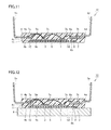
- FIG. 1 is a cross-sectional diagram schematically illustrating a configuration of a power semiconductor device according to a first embodiment of the present invention.
- FIG. 2 is a plan diagram schematically illustrating the configuration of the power semiconductor device according to the first embodiment of the present invention.
- FIG. 3 is a cross-sectional diagram schematically illustrating a configuration of a power semiconductor device according to a second embodiment of the present invention.
- FIG. 4 is a cross-sectional diagram schematically illustrating a configuration of a power semiconductor device according to a third embodiment of the present invention.
- FIG. 5 is a plan diagram schematically illustrating the configuration of the power semiconductor device according to the second and third embodiments of the present invention.
- FIG. 6 is a cross-sectional diagram schematically illustrating a configuration of a power semiconductor device according to a fourth embodiment of the present invention.
- FIG. 7 is a plan diagram schematically illustrating the configuration of the power semiconductor device according to the present invention.
- FIG. 8 is a cross-sectional diagram schematically illustrating a configuration of a power semiconductor device according to a fifth embodiment of the present invention.
- FIG. 9 is a plan diagram schematically illustrating the configuration of the power semiconductor device according to the fifth embodiment of the present invention.
- FIG. 10 is a plan diagram schematically illustrating a configuration of a power semiconductor device according to a sixth embodiment of the present invention.
- FIG. 11 is a cross-sectional diagram schematically illustrating a configuration of a power semiconductor device according to a seventh embodiment of the present invention.
- FIG. 12 is a cross-sectional diagram schematically illustrating the configuration of the power semiconductor device according to the seventh embodiment of the present invention.
- FIG. 13 is a plan diagram schematically illustrating the configuration of the power semiconductor device according to the seventh embodiment of the present invention.
- FIGS. 14 and 15 are schematic plan diagrams illustrating the steps of a method of manufacturing the power semiconductor device according to the first embodiment of the present invention.
- FIG. 16 is a cross-sectional diagram schematically illustrating the second step of the method of manufacturing the power semiconductor device according to the first embodiment of the present invention.
- a power semiconductor module 10 according to the first embodiment mainly includes an IGBT 1 , an IC (Integrated Circuit) 2 , an FWDi (Free Wheeling Diode) 3 , a first frame portion 5 , a second frame portion 6 , a wire 7 a , and an insulator portion 4 .
- the first frame portion 5 has a first surface 5 a and a second surface 5 b opposed to each other.
- Power semiconductor elements such as IGBT 1 and FWDi 3 are mounted on first surface 5 a of first frame portion 5 .
- IGBT 1 and FWDi 3 are each joined to first surface 5 a , for example, with a joint member such as solder.
- the second frame portion 6 has a third surface 6 a and a fourth surface 6 b opposed to each other.
- IC 2 that is a control integrated circuit for controlling the power semiconductor elements is mounted on third surface 6 a of second frame 6 .
- the back surface of IC 2 is joined to third surface 6 a , for example, with a joint member such as solder.
- Second frame portion 6 may serve as a ground potential. As shown in FIG. 2 , two ICs 2 may be mounted on one second frame portion 6 .
- a temperature sensor may be contained in IC 2 .
- IGBT 1 and IC 2 are directly electrically connected with each other by wire 7 a .
- Wire 7 a has one end and the other end. The one end is connected to IGBT 1 and the other end is connected to IC 2 .
- Wire 7 a is arranged to extend between first frame portion 5 and the second frame. As shown in FIG. 2 , three IGBTs 1 may be connected to one IC by wires 7 a . One or more than one wires 7 a may be provided.
- IGBT 1 and FWDi 3 are also electrically connected with each other by wires 7 c . FWDi 3 may be electrically connected with first frame portion 5 by a wire 7 d or may be electrically connected with another frame different from first frame portion 5 .
- IC 2 may be electrically connected with second frame portion 6 by a wire 7 b or may be electrically connected with another frame different from second frame portion 6 .
- Wires 7 a to 7 d are formed of a material, for example, including gold or may be, for example, aluminum. The use of aluminum, which is cheaper than gold, can reduce manufacturing costs of power semiconductor module 10 .
- Insulator portion 4 seals IGBT 1 , FWDi 3 , IC 2 , first frame portion 5 , second frame portion 6 , and wires 7 a to 7 d .
- Insulator portion 4 is formed of, for example, resin but may be ceramic or the like.
- first surface portion 5 a of first frame portion 5 and third surface 6 a of second frame portion 6 are located at the same height in the direction vertical to first surface 5 a of first frame portion 5 (that is, the up-down direction in FIG. 1 ).
- the same height means that the distance between first surface 5 a and third surface 6 a in the direction vertical to first surface 5 a is 0.1 mm or less. That is, first surface 5 a may be located closer to an insulating sheet 11 by 0.1 mm or less or may be located further from insulating sheet 11 by 0.1 mm or less than third surface 6 a.
- first frame portion 5 and second frame portion 6 is bended in the direction vertical to first surface 5 a of first frame portion 5 in the inside of insulator portion 4 .
- First frame portion 5 emerges from a left surface portion 4 c of insulator portion 4 to the outside of insulator portion 4 and connects to a terminal portion 5 e .
- second frame portion 6 emerges from a right surface portion 4 d of insulator portion 4 to the outside of insulator portion 4 and connects to a terminal portion 6 e .
- First frame portion 5 and terminal portion 5 e may be integrally formed or may be separate.
- second frame portion 6 and terminal portion 6 e may be integrally formed or may be separate.
- Power semiconductor module 10 has insulating sheet 11 in contact with second surface 5 b of first frame portion 5 and fourth surface 6 b of second frame portion 6 .
- insulating sheet 11 entirely covers second surface 5 b and fourth surface 6 b .
- a metal plate 12 is arranged in contact with the surface of insulating sheet 11 that is opposite to the surface in contact with first frame portion 5 .
- Metal plate 12 is exposed from insulator portion 4 .
- a heat sink fin 8 is provided in contact with a lower surface 4 b of insulator portion 4 and metal plate 12 .
- FIGS. 1 , 2 , and 14 to 16 A method of manufacturing a power semiconductor module according to the present embodiment will now be described with reference to FIGS. 1 , 2 , and 14 to 16 .
- a frame preparation step is carried out. Specifically, a metal frame 20 having an H-shaped notch portion formed at the center is prepared. Frame 20 has first frame portion 5 having a first end surface 5 f and second frame portion 6 having a second end surface 6 f facing first end surface 5 f with a gap G 1 interposed therebetween. Frame 20 has a third frame portion 9 that is arranged at each side portion of first frame portion 5 and second frame portion 6 with a gap G 2 interposed and couples first frame portion 5 and second frame portion 6 .
- a step of mounting a power semiconductor element on first frame portion 5 and a step of mounting a control integrated circuit for controlling the power semiconductor element on second frame portion 6 are carried out.
- IGBT 1 and FWDi are mounted on first surface 5 a of first frame portion 5
- IC 2 is mounted on third surface 6 a of second frame portion 6 .
- a frame bending step is carried out. Specifically, first frame portion 5 and second frame portion 6 are bent with respect to third frame portion 9 in a direction crossing third frame portion 9 , and third frame portion 9 is shrunken in a direction in which first end surface 5 f and second end surface 6 f face each other.
- Shrinking third frame portion 9 means that the width of frame 20 is reduced from a width d 1 to a width d 2 .
- a curved portion 9 a may be formed in the vicinity of the center of third frame portion 9 by shrinking third frame portion 9 .
- First frame portion 5 is bent at a first bend portion 5 c toward insulating sheet 11 and bent at a second bend portion 5 d opposite to insulating sheet 11 .
- second frame portion 6 is bent at a first bend portion 6 c toward insulating sheet 11 and bent at a second bend portion 6 d opposite to insulating sheet 11 .
- first frame portion 5 and second frame portion 6 are located at the same height in the direction normal to first surface 5 a (that is, in the up-down direction in FIG. 16 ).
- Third frame portion 9 that connects first frame portion 5 and second frame portion 6 is thereafter removed whereby first frame portion 5 and second frame portion 6 are electrically isolated from each other.
- a wire bonding step is carried out. Specifically, wire 7 a having one end and the other end is used so that one end of wire 7 a is connected to IGBT 1 and the other end of wire 7 a is connected to IC 2 . IGBT 1 and IC 2 are thus directly electrically connected with each other by wire 7 a . IGBT 1 and FWDi 3 are electrically connected by wire 7 c . FWDi 3 and first frame portion 5 may be electrically connected by wire 7 d . In addition, IC 2 and second frame portion 6 may be electrically connected by wire 7 b.
- IGBT 1 , FWDi 3 , IC 2 , first frame 5 , second frame portion 6 , and wires 7 a to 7 d are sealed with insulator portion 4 formed of resin.
- the frame bending step is carried out after the step of mounting the power semiconductor element and the step of mounting the control integrated circuit.
- the step of mounting the power semiconductor element and the step of mounting the control integrated circuit may be carried out after the frame bending step.
- Power semiconductor module 10 has wire 7 a coupling the power semiconductor element and the control integrated circuit, and first surface 5 a of first frame portion 5 having the power semiconductor element mounted thereon and third surface 6 a of second frame portion 6 having the control integrated circuit mounted thereon are located at the same height. This can alleviate stress exerted on the end portion of wire 7 a and thus stabilizes the loop of wire 7 a thereby preventing a disconnection of wire 7 a and wire 7 a from short-circuiting with the other frame. In addition, wire 7 a is prevented from flowing when insulator portion 4 is molded. In a case where a temperature sensor is mounted on the control integrated circuit, the accuracy of the temperature sensor can be improved because the distance between the temperature sensor and the power semiconductor element is short.
- Power semiconductor module 10 according to the first embodiment further includes insulating sheet 11 in contact with second surface 5 b of first frame portion 5 and fourth surface 6 b of second frame portion 6 . Accordingly, heat can be dissipated efficiently through second surface 5 b and fourth surface 6 b.
- first frame portion 5 and second frame portion 6 are bent with respect to third frame portion 9 , and third frame portion 9 is shrunken in the direction in which first end surface 5 f and second end surface 6 f face each other. This can minimize the distance between the power semiconductor element and the control integrated circuit in the direction parallel to first surface 5 a and minimize the distance between the power semiconductor element and the integrated control circuit in the direction vertical to the first surface.
- the configuration of power semiconductor module 10 according to the second embodiment differs from the configuration of the power semiconductor module according to the first embodiment in that a block portion 13 made of copper is arranged between first frame portion 5 and insulating sheet 11 .
- the other configuration is the same as the first embodiment.
- block portion 13 made of copper is arranged in contact with second surface 5 b of first frame portion 5 and insulating sheet 11 .
- First frame portion 5 having IGBT 1 and FWDi 3 mounted thereon and second frame portion 6 having IC 2 mounted thereon are located at the same height in the direction normal to first surface 5 a of the first frame portion.
- Second frame portion 6 is in contact with insulating sheet 11 with insulator portion 4 interposed therebetween.
- Power semiconductor module 10 has block portion 13 in contact with second surface 5 b of first frame portion 5 . Accordingly, first surface 5 a of first frame portion 5 and third surface 6 a of second frame portion 6 can be positioned at the same height in the direction vertical to first surface 5 a without bending second frame portion 6 in the inside of insulator portion 4 . As a result, the loop of wire 7 a coupling the power semiconductor element and the control integrated circuit can be stabilized.
- the material of block portion 13 includes copper. Accordingly, heat generated by the power semiconductor element can be efficiently diffused to the outside.
- the configuration of the power semiconductor module according to the third embodiment differs from the configuration of the power semiconductor module according to the second embodiment in that block portion 13 has a DBC (Direct Bonded Copper) structure because of inclusion of ceramic.
- the other configuration is the same as the second embodiment.
- the DBC has a ceramic base arranged between two copper plates and bonded to the copper plates.
- power semiconductor module 10 according to the third embodiment has a block portion arranged between first frame portion 5 made of copper and metal plate 12 made of copper.
- the block portion is formed of a ceramic base 14 of aluminum oxide (Al 2 O 3 ), aluminum nitride (AlN), or the like.
- First frame portion 5 having IGBT 1 and FWDi 3 mounted thereon and second frame portion 6 having IC 2 mounted thereon are located at the same height in the direction normal to first surface 5 a of the first frame portion.
- Second frame portion 6 is in contact with insulating sheet 11 with insulator portion 4 interposed therebetween.
- the material of block portion 13 includes ceramic. This can reduce the weight of power semiconductor module 10 .
- the configuration of the power semiconductor module according to the fourth embodiment differs from the configuration of the power semiconductor module according to the first embodiment in that at least one of first frame portion 5 and second frame portion 6 emerges to the outside of the insulator portion from upper surface 4 a of insulator portion 4 on the side facing first surface 5 a .
- the other configuration is the same as the first embodiment.
- first frame portion 5 in power semiconductor module 10 is bent toward upper surface 4 a of insulator portion 4 in the inside of insulator portion 4 .
- First frame portion 5 emerges to the outside of insulator portion 4 through upper surface 4 a of insulator portion 4 .
- second frame portion 6 is bent toward upper surface 4 a of insulator portion 4 in the inside of insulator portion 4 .
- Second frame portion 6 emerges to the outside of insulator portion 4 through upper surface 4 a of insulator portion 4 .
- first frame portion 5 and second frame portion 6 each emerges to the outside through upper surface 4 a of insulator portion 4 .
- one of first frame portion 5 and second frame portion 6 may pass through upper surface 4 a of insulator portion 4 and the other may pass through left surface portion 4 c or right surface portion 4 d of insulator portion 4 to emerge to the outside.
- first frame portion 5 and second frame portion 6 emerges to the outside of insulator portion 4 from upper surface 4 a of insulator portion 4 that faces first surface 5 a .
- This increases the distance between first frame portion 5 and second frame portion 6 , and heat sink fin 8 thereby improving the insulation between first frame portion 5 and second frame portion 6 , and heat sink fin 8 .
- the configuration of the power semiconductor module according to the fifth embodiment differs from the configuration of the power semiconductor module according to the first embodiment in that at least one of first frame portion 5 and second frame portion 6 has a connector pin 15 at a position exposed from insulator portion 4 to the outside.
- the other configuration is the same as the first embodiment.
- first frame portion 5 and second frame portion 6 each have a connector pin 15 .
- connector pin 15 is partially exposed from upper surface 4 a of insulator portion 4 , and connector pin 15 is connected with terminal portion 5 e .
- First frame portion 5 and terminal portion 5 e are thus electrically connected with each other.
- connector pin 15 is connected with terminal portion 6 e .
- second frame portion 6 and terminal portion 6 e are thus electrically connected with each other.
- Terminal portion 5 e and terminal portion 6 e extend in the direction crossing upper surface 4 a of insulator portion 4 .
- first frame portion 5 and second frame portion 6 each have connector pin 15 .
- one of first frame portion 5 and second frame portion 6 may have connector pin 15 , and the other may not have connector pin 15 .
- first frame portion 5 and second frame portion 6 has connector pin 15 at a position exposed from insulator portion 4 to the outside.
- First frame portion 5 and second frame portion 6 are formed as frames without terminals, and terminal portions 5 e and 6 e are attached thereto through connector pins 15 in the subsequent step, whereby power semiconductor module 10 having terminal portions different in shape can be manufactured efficiently.
- first frame portion 5 and second frame portion 6 formed as frames without terminals, a multi-row frame, for example, in a staggered arrangement can be formed.
- the configuration of the power semiconductor module according to the sixth embodiment differs from the configuration of the first embodiment in that IC 2 is a single chip.
- the other configuration is the same as the first embodiment.
- a single IC 2 mounted on second frame portion 6 is provided to be able to control a plurality of IGBTs 1 .
- two IGBTs 1 mounted above and below are controlled by separate ICs 2 , so that mutual operation timings cannot be controlled.
- two IGBTs 1 arranged above and below are controlled in the inside of IC 2 so as not to operate simultaneously, thereby achieving a function as an interlock (safety device).
- the configuration of the power semiconductor module according to the seventh embodiment differs from the configuration of the power semiconductor module according to the first embodiment in that second frame portion 6 and insulating sheet 11 are not in direct contact with each other, and that second frame portion 6 is located closer to upper surface 4 a of insulator portion 4 than first frame portion 5 .
- the other configuration is the same as the first embodiment.
- a method of manufacturing the power semiconductor module according to the seventh embodiment is similar to the manufacturing method in the first embodiment.
- insulator portion 4 is arranged between fourth surface 6 b of second frame portion 6 and insulating sheet 11 .
- Second frame portion 6 is bent in the inside of insulator portion 4 in the direction crossing first surface 5 a of first frame portion 5 .
- First frame portion 5 having IGBT 1 and FWDi 3 mounted thereon is arranged closer to insulating sheet 11 than second frame portion 6 having IC 2 mounted thereon. That is, in the power semiconductor module according to the seventh embodiment, the distance between first surface 5 a of first frame portion 5 and third surface 6 a of second frame portion 6 may not be the same in the direction vertical to first surface 5 a.
- metal plate 12 in contact with insulating sheet 11 may be exposed to the outside of insulator portion 4 as shown in FIG. 11 .
- heat sink fin 8 is provided in contact with metal plate 12 and lower surface 4 b of insulator portion 4 .
- second frame portion 6 is bent in the inside of insulator portion 4 in the direction crossing first surface 5 a . This can reduce the distance between first frame portion 5 and second frame portion 6 in the direction vertical to first surface 5 a , thereby stabilizing the loop of wire 7 a coupling the power semiconductor element and the control integrated circuit. As a result, a disconnection of wire 7 a or a shirt circuit can be prevented.
Landscapes
- Engineering & Computer Science (AREA)
- Microelectronics & Electronic Packaging (AREA)
- General Physics & Mathematics (AREA)
- Physics & Mathematics (AREA)
- Computer Hardware Design (AREA)
- Condensed Matter Physics & Semiconductors (AREA)
- Power Engineering (AREA)
- Chemical & Material Sciences (AREA)
- Manufacturing & Machinery (AREA)
- Ceramic Engineering (AREA)
- Materials Engineering (AREA)
- Cooling Or The Like Of Semiconductors Or Solid State Devices (AREA)
- Inverter Devices (AREA)
- Wire Bonding (AREA)
Priority Applications (1)
| Application Number | Priority Date | Filing Date | Title |
|---|---|---|---|
| US14/796,843 US9252028B2 (en) | 2012-11-15 | 2015-07-10 | Power semiconductor module and method of manufacturing the same |
Applications Claiming Priority (2)
| Application Number | Priority Date | Filing Date | Title |
|---|---|---|---|
| JP2012-251225 | 2012-11-15 | ||
| JP2012251225A JP2014099547A (ja) | 2012-11-15 | 2012-11-15 | 電力半導体モジュールおよびその製造方法 |
Related Child Applications (1)
| Application Number | Title | Priority Date | Filing Date |
|---|---|---|---|
| US14/796,843 Division US9252028B2 (en) | 2012-11-15 | 2015-07-10 | Power semiconductor module and method of manufacturing the same |
Publications (2)
| Publication Number | Publication Date |
|---|---|
| US20140131846A1 US20140131846A1 (en) | 2014-05-15 |
| US9171774B2 true US9171774B2 (en) | 2015-10-27 |
Family
ID=50680929
Family Applications (2)
| Application Number | Title | Priority Date | Filing Date |
|---|---|---|---|
| US14/027,014 Active US9171774B2 (en) | 2012-11-15 | 2013-09-13 | Power semiconductor module and method of manufacturing the same |
| US14/796,843 Active US9252028B2 (en) | 2012-11-15 | 2015-07-10 | Power semiconductor module and method of manufacturing the same |
Family Applications After (1)
| Application Number | Title | Priority Date | Filing Date |
|---|---|---|---|
| US14/796,843 Active US9252028B2 (en) | 2012-11-15 | 2015-07-10 | Power semiconductor module and method of manufacturing the same |
Country Status (4)
| Country | Link |
|---|---|
| US (2) | US9171774B2 (ja) |
| JP (1) | JP2014099547A (ja) |
| KR (1) | KR101513961B1 (ja) |
| CN (1) | CN103824844A (ja) |
Families Citing this family (19)
| Publication number | Priority date | Publication date | Assignee | Title |
|---|---|---|---|---|
| US9524928B2 (en) | 2010-12-13 | 2016-12-20 | Infineon Technologies Americas Corp. | Power quad flat no-lead (PQFN) package having control and driver circuits |
| US9362215B2 (en) | 2010-12-13 | 2016-06-07 | Infineon Technologies Americas Corp. | Power quad flat no-lead (PQFN) semiconductor package with leadframe islands for multi-phase power inverter |
| US9659845B2 (en) | 2010-12-13 | 2017-05-23 | Infineon Technologies Americas Corp. | Power quad flat no-lead (PQFN) package in a single shunt inverter circuit |
| US9711437B2 (en) * | 2010-12-13 | 2017-07-18 | Infineon Technologies Americas Corp. | Semiconductor package having multi-phase power inverter with internal temperature sensor |
| US9355995B2 (en) | 2010-12-13 | 2016-05-31 | Infineon Technologies Americas Corp. | Semiconductor packages utilizing leadframe panels with grooves in connecting bars |
| US8587101B2 (en) | 2010-12-13 | 2013-11-19 | International Rectifier Corporation | Multi-chip module (MCM) power quad flat no-lead (PQFN) semiconductor package utilizing a leadframe for electrical interconnections |
| US9443795B2 (en) | 2010-12-13 | 2016-09-13 | Infineon Technologies Americas Corp. | Power quad flat no-lead (PQFN) package having bootstrap diodes on a common integrated circuit (IC) |
| US9620954B2 (en) | 2010-12-13 | 2017-04-11 | Infineon Technologies Americas Corp. | Semiconductor package having an over-temperature protection circuit utilizing multiple temperature threshold values |
| US9449957B2 (en) | 2010-12-13 | 2016-09-20 | Infineon Technologies Americas Corp. | Control and driver circuits on a power quad flat no-lead (PQFN) leadframe |
| DE112014006142B4 (de) * | 2014-01-10 | 2024-01-18 | Mitsubishi Electric Corporation | Leistungshalbleiteranordnung |
| DE112014007140B4 (de) | 2014-11-07 | 2024-05-02 | Mitsubishi Electric Corporation | Leistungshalbleiteranordnung und Verfahren zum Herstellen derselben |
| DE102015102041A1 (de) * | 2015-02-12 | 2016-08-18 | Danfoss Silicon Power Gmbh | Leistungsmodul |
| CN105990266B (zh) * | 2015-02-26 | 2018-12-07 | 台达电子工业股份有限公司 | 功率转换电路的封装模块及其制造方法 |
| US10679929B2 (en) | 2017-07-28 | 2020-06-09 | Advanced Semiconductor Engineering Korea, Inc. | Semiconductor package device and method of manufacturing the same |
| US10396774B2 (en) | 2017-09-14 | 2019-08-27 | Hestia Power Inc. | Intelligent power module operable to be driven by negative gate voltage |
| TWI640151B (zh) * | 2017-09-20 | 2018-11-01 | 瀚薪科技股份有限公司 | Negative voltage gate driven smart power module |
| US10714418B2 (en) * | 2018-03-26 | 2020-07-14 | Texas Instruments Incorporated | Electronic device having inverted lead pins |
| CN109449150A (zh) * | 2018-12-11 | 2019-03-08 | 杰群电子科技(东莞)有限公司 | 带引脚封装、无引脚封装的功率模块及其对应加工方法 |
| TWI693682B (zh) * | 2019-08-28 | 2020-05-11 | 財團法人工業技術研究院 | 電子元件封裝結構 |
Citations (11)
| Publication number | Priority date | Publication date | Assignee | Title |
|---|---|---|---|---|
| JPH09186269A (ja) | 1996-01-05 | 1997-07-15 | Hitachi Ltd | 半導体装置 |
| JPH09283681A (ja) | 1996-04-16 | 1997-10-31 | Hitachi Ltd | 半導体装置 |
| US20030075783A1 (en) | 2001-10-19 | 2003-04-24 | Mitsubishi Denki Kabushiki Kaisha | Semiconductor device |
| JP2005005638A (ja) | 2003-04-15 | 2005-01-06 | Fuji Electric Fa Components & Systems Co Ltd | 半導体モジュールおよびその製造方法 |
| JP2005150595A (ja) | 2003-11-19 | 2005-06-09 | Mitsubishi Electric Corp | 電力用半導体装置 |
| KR20060017711A (ko) | 2004-08-21 | 2006-02-27 | 페어차일드코리아반도체 주식회사 | 높은 열 방출 능력을 구비한 전력용 모듈 패키지 및 그제조방법 |
| JP2006080300A (ja) | 2004-09-09 | 2006-03-23 | Kokusan Denki Co Ltd | リードフレーム及びその製造方法 |
| US20080054422A1 (en) | 2006-08-30 | 2008-03-06 | Nobuya Koike | Semiconductor device |
| KR20090093163A (ko) | 2008-02-28 | 2009-09-02 | 페어차일드코리아반도체 주식회사 | 전력 소자 패키지 및 그 제조 방법 |
| WO2009110376A1 (ja) | 2008-03-06 | 2009-09-11 | 三菱電機株式会社 | リードフレーム基板、半導体モジュール、及びリードフレーム基板の製造方法 |
| US20140001611A1 (en) * | 2012-06-29 | 2014-01-02 | Samsung Electro-Mechanics Co. Ltd. | Semiconductor package |
Family Cites Families (2)
| Publication number | Priority date | Publication date | Assignee | Title |
|---|---|---|---|---|
| DE19735531A1 (de) * | 1997-08-16 | 1999-02-18 | Abb Research Ltd | Leistungshalbleitermodul mit in Submodulen integrierten Kühlern |
| US6870243B2 (en) * | 2002-11-27 | 2005-03-22 | Freescale Semiconductor, Inc. | Thin GaAs die with copper back-metal structure |
-
2012
- 2012-11-15 JP JP2012251225A patent/JP2014099547A/ja active Pending
-
2013
- 2013-09-13 US US14/027,014 patent/US9171774B2/en active Active
- 2013-11-08 KR KR1020130135224A patent/KR101513961B1/ko not_active IP Right Cessation
- 2013-11-15 CN CN201310575019.4A patent/CN103824844A/zh active Pending
-
2015
- 2015-07-10 US US14/796,843 patent/US9252028B2/en active Active
Patent Citations (16)
| Publication number | Priority date | Publication date | Assignee | Title |
|---|---|---|---|---|
| JPH09186269A (ja) | 1996-01-05 | 1997-07-15 | Hitachi Ltd | 半導体装置 |
| JPH09283681A (ja) | 1996-04-16 | 1997-10-31 | Hitachi Ltd | 半導体装置 |
| US20030075783A1 (en) | 2001-10-19 | 2003-04-24 | Mitsubishi Denki Kabushiki Kaisha | Semiconductor device |
| JP2003124437A (ja) | 2001-10-19 | 2003-04-25 | Mitsubishi Electric Corp | 半導体装置 |
| KR20030032816A (ko) | 2001-10-19 | 2003-04-26 | 미쓰비시덴키 가부시키가이샤 | 반도체장치 |
| JP2005005638A (ja) | 2003-04-15 | 2005-01-06 | Fuji Electric Fa Components & Systems Co Ltd | 半導体モジュールおよびその製造方法 |
| JP2005150595A (ja) | 2003-11-19 | 2005-06-09 | Mitsubishi Electric Corp | 電力用半導体装置 |
| KR20060017711A (ko) | 2004-08-21 | 2006-02-27 | 페어차일드코리아반도체 주식회사 | 높은 열 방출 능력을 구비한 전력용 모듈 패키지 및 그제조방법 |
| US20060056213A1 (en) | 2004-08-21 | 2006-03-16 | Joosang Lee | Power module package having excellent heat sink emission capability and method for manufacturing the same |
| JP2006080300A (ja) | 2004-09-09 | 2006-03-23 | Kokusan Denki Co Ltd | リードフレーム及びその製造方法 |
| US20080054422A1 (en) | 2006-08-30 | 2008-03-06 | Nobuya Koike | Semiconductor device |
| JP2008060256A (ja) | 2006-08-30 | 2008-03-13 | Renesas Technology Corp | 半導体装置 |
| KR20090093163A (ko) | 2008-02-28 | 2009-09-02 | 페어차일드코리아반도체 주식회사 | 전력 소자 패키지 및 그 제조 방법 |
| US20090218666A1 (en) | 2008-02-28 | 2009-09-03 | Yang Gwi-Gyeon | Power device package and method of fabricating the same |
| WO2009110376A1 (ja) | 2008-03-06 | 2009-09-11 | 三菱電機株式会社 | リードフレーム基板、半導体モジュール、及びリードフレーム基板の製造方法 |
| US20140001611A1 (en) * | 2012-06-29 | 2014-01-02 | Samsung Electro-Mechanics Co. Ltd. | Semiconductor package |
Non-Patent Citations (3)
| Title |
|---|
| An Office Action; "Grounds for Rejection," issued by the Korean Patent Office on Jul. 30, 2014, which corresponds to Korean Patent Application No. 10-2013-0135224 and is related to U.S. Appl. No. 14/027,014; with English language translation. |
| An Office Action; "Notice of Allowance," issued by the Korean Patent Office on Feb. 27, 2015, which corresponds to Korean Patent Application No. 10-2013-0135224 and is related to U.S. Appl. No. 14/027,014; with English language translation. |
| An Office Action; "Notice of Grounds of Rejection," issued by the Japanese Patent Office on Jul. 28, 2015, which corresponds to Japanese Patent Application No. 2012-251225 and is related to U.S. Appl. No. 14/027,014; with English language translation. |
Also Published As
| Publication number | Publication date |
|---|---|
| KR20140066090A (ko) | 2014-05-30 |
| CN103824844A (zh) | 2014-05-28 |
| US9252028B2 (en) | 2016-02-02 |
| US20140131846A1 (en) | 2014-05-15 |
| US20150318189A1 (en) | 2015-11-05 |
| JP2014099547A (ja) | 2014-05-29 |
| KR101513961B1 (ko) | 2015-04-21 |
Similar Documents
| Publication | Publication Date | Title |
|---|---|---|
| US9252028B2 (en) | Power semiconductor module and method of manufacturing the same | |
| US9391006B2 (en) | Semiconductor device and method of manufacturing semiconductor device | |
| JP6522402B2 (ja) | 半導体装置 | |
| US7582958B2 (en) | Semiconductor package | |
| US9613888B2 (en) | Semiconductor device and semiconductor module | |
| US8981552B2 (en) | Power converter, semiconductor device, and method for manufacturing power converter | |
| US9431326B2 (en) | Semiconductor device and manufacturing method thereof | |
| US9196577B2 (en) | Semiconductor packaging arrangement | |
| US10529656B2 (en) | Semiconductor device | |
| US11037856B2 (en) | Semiconductor chip package comprising a leadframe connected to a substrate and a semiconductor chip, and a method for fabricating the same | |
| CN108155168B (zh) | 电子器件 | |
| US11189547B2 (en) | Semiconductor module and semiconductor module manufacturing method | |
| CN102412211A (zh) | 电子器件 | |
| CN111883490A (zh) | 具有用于顶侧冷却的多级传导夹的半导体封装 | |
| US10083899B2 (en) | Semiconductor package with heat slug and rivet free die attach area | |
| US20230327350A1 (en) | Transfer molded power modules and methods of manufacture | |
| US9685396B2 (en) | Semiconductor die arrangement | |
| US10790242B2 (en) | Method of manufacturing a semiconductor device | |
| US20120217655A1 (en) | Electronic device for high power applications | |
| US11302569B2 (en) | Method for manufacturing semiconductor device and semiconductor device | |
| US10847489B2 (en) | Semiconductor device | |
| JP6647187B2 (ja) | パワーモジュールおよびその製造方法 | |
| JP2023076113A (ja) | 半導体装置 | |
| CN111987050A (zh) | 具有节省空间的引线和管芯焊盘设计的半导体封装 | |
| KR19980020728A (ko) | 열방출 리드를 갖는 반도체 칩 패키지용 리드 프레임 |
Legal Events
| Date | Code | Title | Description |
|---|---|---|---|
| AS | Assignment |
Owner name: MITSUBISHI ELECTRIC CORPORATION, JAPAN Free format text: ASSIGNMENT OF ASSIGNORS INTEREST;ASSIGNORS:SHIRAMIZU, MASATAKA;MING, SHANG;REEL/FRAME:031224/0563 Effective date: 20130724 |
|
| AS | Assignment |
Owner name: MITSUBISHI ELECTRIC CORPORATION, JAPAN Free format text: CORRECTIVE ASSIGNMENT TO CORRECT THE SECOND INVENTOR'S NAME PREVIOUSLY RECORDED ON REEL 031224 FRAME 0563. ASSIGNOR(S) HEREBY CONFIRMS THE ASSIGNMENT;ASSIGNORS:SHIRAMIZU, MASATAKA;SHANG, MING;REEL/FRAME:031867/0052 Effective date: 20130724 |
|
| STCF | Information on status: patent grant |
Free format text: PATENTED CASE |
|
| MAFP | Maintenance fee payment |
Free format text: PAYMENT OF MAINTENANCE FEE, 4TH YEAR, LARGE ENTITY (ORIGINAL EVENT CODE: M1551); ENTITY STATUS OF PATENT OWNER: LARGE ENTITY Year of fee payment: 4 |
|
| AS | Assignment |
Owner name: ARIGNA TECHNOLOGY LIMITED, IRELAND Free format text: ASSIGNMENT OF ASSIGNORS INTEREST;ASSIGNOR:MITSUBISHI ELECTRIC CORPORATION;REEL/FRAME:052042/0651 Effective date: 20200213 |
|
| MAFP | Maintenance fee payment |
Free format text: PAYMENT OF MAINTENANCE FEE, 8TH YEAR, LARGE ENTITY (ORIGINAL EVENT CODE: M1552); ENTITY STATUS OF PATENT OWNER: LARGE ENTITY Year of fee payment: 8 |