US9685396B2 - Semiconductor die arrangement - Google Patents
Semiconductor die arrangement Download PDFInfo
- Publication number
- US9685396B2 US9685396B2 US14/865,985 US201514865985A US9685396B2 US 9685396 B2 US9685396 B2 US 9685396B2 US 201514865985 A US201514865985 A US 201514865985A US 9685396 B2 US9685396 B2 US 9685396B2
- Authority
- US
- United States
- Prior art keywords
- die
- terminal
- semiconductor device
- semiconductor
- electrically connected
- Prior art date
- Legal status (The legal status is an assumption and is not a legal conclusion. Google has not performed a legal analysis and makes no representation as to the accuracy of the status listed.)
- Active
Links
Images


Classifications
-
- H—ELECTRICITY
- H10—SEMICONDUCTOR DEVICES; ELECTRIC SOLID-STATE DEVICES NOT OTHERWISE PROVIDED FOR
- H10W—GENERIC PACKAGES, INTERCONNECTIONS, CONNECTORS OR OTHER CONSTRUCTIONAL DETAILS OF DEVICES COVERED BY CLASS H10
- H10W70/00—Package substrates; Interposers; Redistribution layers [RDL]
- H10W70/40—Leadframes
- H10W70/411—Chip-supporting parts, e.g. die pads
- H10W70/415—Leadframe inner leads serving as die pads
-
- H01L23/4951—
-
- H01L21/4825—
-
- H01L21/565—
-
- H01L23/3114—
-
- H01L23/49513—
-
- H01L23/4952—
-
- H01L23/49562—
-
- H01L23/49575—
-
- H01L24/48—
-
- H01L25/0657—
-
- H—ELECTRICITY
- H10—SEMICONDUCTOR DEVICES; ELECTRIC SOLID-STATE DEVICES NOT OTHERWISE PROVIDED FOR
- H10W—GENERIC PACKAGES, INTERCONNECTIONS, CONNECTORS OR OTHER CONSTRUCTIONAL DETAILS OF DEVICES COVERED BY CLASS H10
- H10W70/00—Package substrates; Interposers; Redistribution layers [RDL]
- H10W70/01—Manufacture or treatment
- H10W70/04—Manufacture or treatment of leadframes
- H10W70/041—Connecting or disconnecting interconnections to or from leadframes, e.g. connecting bond wires or bumps
-
- H—ELECTRICITY
- H10—SEMICONDUCTOR DEVICES; ELECTRIC SOLID-STATE DEVICES NOT OTHERWISE PROVIDED FOR
- H10W—GENERIC PACKAGES, INTERCONNECTIONS, CONNECTORS OR OTHER CONSTRUCTIONAL DETAILS OF DEVICES COVERED BY CLASS H10
- H10W70/00—Package substrates; Interposers; Redistribution layers [RDL]
- H10W70/40—Leadframes
- H10W70/411—Chip-supporting parts, e.g. die pads
- H10W70/417—Bonding materials between chips and die pads
-
- H—ELECTRICITY
- H10—SEMICONDUCTOR DEVICES; ELECTRIC SOLID-STATE DEVICES NOT OTHERWISE PROVIDED FOR
- H10W—GENERIC PACKAGES, INTERCONNECTIONS, CONNECTORS OR OTHER CONSTRUCTIONAL DETAILS OF DEVICES COVERED BY CLASS H10
- H10W70/00—Package substrates; Interposers; Redistribution layers [RDL]
- H10W70/40—Leadframes
- H10W70/464—Additional interconnections in combination with leadframes
- H10W70/465—Bumps or wires
-
- H—ELECTRICITY
- H10—SEMICONDUCTOR DEVICES; ELECTRIC SOLID-STATE DEVICES NOT OTHERWISE PROVIDED FOR
- H10W—GENERIC PACKAGES, INTERCONNECTIONS, CONNECTORS OR OTHER CONSTRUCTIONAL DETAILS OF DEVICES COVERED BY CLASS H10
- H10W70/00—Package substrates; Interposers; Redistribution layers [RDL]
- H10W70/40—Leadframes
- H10W70/481—Leadframes for devices being provided for in groups H10D8/00 - H10D48/00
-
- H—ELECTRICITY
- H10—SEMICONDUCTOR DEVICES; ELECTRIC SOLID-STATE DEVICES NOT OTHERWISE PROVIDED FOR
- H10W—GENERIC PACKAGES, INTERCONNECTIONS, CONNECTORS OR OTHER CONSTRUCTIONAL DETAILS OF DEVICES COVERED BY CLASS H10
- H10W74/00—Encapsulations, e.g. protective coatings
- H10W74/01—Manufacture or treatment
- H10W74/016—Manufacture or treatment using moulds
-
- H—ELECTRICITY
- H10—SEMICONDUCTOR DEVICES; ELECTRIC SOLID-STATE DEVICES NOT OTHERWISE PROVIDED FOR
- H10W—GENERIC PACKAGES, INTERCONNECTIONS, CONNECTORS OR OTHER CONSTRUCTIONAL DETAILS OF DEVICES COVERED BY CLASS H10
- H10W74/00—Encapsulations, e.g. protective coatings
- H10W74/10—Encapsulations, e.g. protective coatings characterised by their shape or disposition
- H10W74/111—Encapsulations, e.g. protective coatings characterised by their shape or disposition the semiconductor body being completely enclosed
- H10W74/129—Encapsulations, e.g. protective coatings characterised by their shape or disposition the semiconductor body being completely enclosed forming a chip-scale package [CSP]
-
- H—ELECTRICITY
- H10—SEMICONDUCTOR DEVICES; ELECTRIC SOLID-STATE DEVICES NOT OTHERWISE PROVIDED FOR
- H10W—GENERIC PACKAGES, INTERCONNECTIONS, CONNECTORS OR OTHER CONSTRUCTIONAL DETAILS OF DEVICES COVERED BY CLASS H10
- H10W90/00—Package configurations
-
- H—ELECTRICITY
- H10—SEMICONDUCTOR DEVICES; ELECTRIC SOLID-STATE DEVICES NOT OTHERWISE PROVIDED FOR
- H10W—GENERIC PACKAGES, INTERCONNECTIONS, CONNECTORS OR OTHER CONSTRUCTIONAL DETAILS OF DEVICES COVERED BY CLASS H10
- H10W90/00—Package configurations
- H10W90/811—Multiple chips on leadframes
-
- H01L2224/0603—
-
- H01L2224/29101—
-
- H01L2224/32145—
-
- H01L2224/32245—
-
- H01L2224/45099—
-
- H01L2224/48137—
-
- H01L2224/48247—
-
- H01L2224/49171—
-
- H01L2224/73265—
-
- H01L2224/92247—
-
- H01L24/06—
-
- H01L24/29—
-
- H01L24/32—
-
- H01L24/49—
-
- H01L24/73—
-
- H01L2924/00—
-
- H01L2924/00012—
-
- H01L2924/00014—
-
- H01L2924/014—
-
- H01L2924/1203—
-
- H01L2924/1301—
-
- H01L2924/13033—
-
- H01L2924/13034—
-
- H—ELECTRICITY
- H10—SEMICONDUCTOR DEVICES; ELECTRIC SOLID-STATE DEVICES NOT OTHERWISE PROVIDED FOR
- H10W—GENERIC PACKAGES, INTERCONNECTIONS, CONNECTORS OR OTHER CONSTRUCTIONAL DETAILS OF DEVICES COVERED BY CLASS H10
- H10W72/00—Interconnections or connectors in packages
- H10W72/071—Connecting or disconnecting
- H10W72/073—Connecting or disconnecting of die-attach connectors
-
- H—ELECTRICITY
- H10—SEMICONDUCTOR DEVICES; ELECTRIC SOLID-STATE DEVICES NOT OTHERWISE PROVIDED FOR
- H10W—GENERIC PACKAGES, INTERCONNECTIONS, CONNECTORS OR OTHER CONSTRUCTIONAL DETAILS OF DEVICES COVERED BY CLASS H10
- H10W72/00—Interconnections or connectors in packages
- H10W72/071—Connecting or disconnecting
- H10W72/075—Connecting or disconnecting of bond wires
-
- H—ELECTRICITY
- H10—SEMICONDUCTOR DEVICES; ELECTRIC SOLID-STATE DEVICES NOT OTHERWISE PROVIDED FOR
- H10W—GENERIC PACKAGES, INTERCONNECTIONS, CONNECTORS OR OTHER CONSTRUCTIONAL DETAILS OF DEVICES COVERED BY CLASS H10
- H10W72/00—Interconnections or connectors in packages
- H10W72/30—Die-attach connectors
- H10W72/351—Materials of die-attach connectors
- H10W72/352—Materials of die-attach connectors comprising metals or metalloids, e.g. solders
-
- H—ELECTRICITY
- H10—SEMICONDUCTOR DEVICES; ELECTRIC SOLID-STATE DEVICES NOT OTHERWISE PROVIDED FOR
- H10W—GENERIC PACKAGES, INTERCONNECTIONS, CONNECTORS OR OTHER CONSTRUCTIONAL DETAILS OF DEVICES COVERED BY CLASS H10
- H10W72/00—Interconnections or connectors in packages
- H10W72/50—Bond wires
- H10W72/541—Dispositions of bond wires
- H10W72/5449—Dispositions of bond wires not being orthogonal to a side surface of the chip, e.g. fan-out arrangements
-
- H—ELECTRICITY
- H10—SEMICONDUCTOR DEVICES; ELECTRIC SOLID-STATE DEVICES NOT OTHERWISE PROVIDED FOR
- H10W—GENERIC PACKAGES, INTERCONNECTIONS, CONNECTORS OR OTHER CONSTRUCTIONAL DETAILS OF DEVICES COVERED BY CLASS H10
- H10W72/00—Interconnections or connectors in packages
- H10W72/851—Dispositions of multiple connectors or interconnections
- H10W72/874—On different surfaces
- H10W72/884—Die-attach connectors and bond wires
-
- H—ELECTRICITY
- H10—SEMICONDUCTOR DEVICES; ELECTRIC SOLID-STATE DEVICES NOT OTHERWISE PROVIDED FOR
- H10W—GENERIC PACKAGES, INTERCONNECTIONS, CONNECTORS OR OTHER CONSTRUCTIONAL DETAILS OF DEVICES COVERED BY CLASS H10
- H10W72/00—Interconnections or connectors in packages
- H10W72/90—Bond pads, in general
- H10W72/921—Structures or relative sizes of bond pads
- H10W72/926—Multiple bond pads having different sizes
-
- H—ELECTRICITY
- H10—SEMICONDUCTOR DEVICES; ELECTRIC SOLID-STATE DEVICES NOT OTHERWISE PROVIDED FOR
- H10W—GENERIC PACKAGES, INTERCONNECTIONS, CONNECTORS OR OTHER CONSTRUCTIONAL DETAILS OF DEVICES COVERED BY CLASS H10
- H10W72/00—Interconnections or connectors in packages
- H10W72/90—Bond pads, in general
- H10W72/931—Shapes of bond pads
- H10W72/932—Plan-view shape, i.e. in top view
-
- H—ELECTRICITY
- H10—SEMICONDUCTOR DEVICES; ELECTRIC SOLID-STATE DEVICES NOT OTHERWISE PROVIDED FOR
- H10W—GENERIC PACKAGES, INTERCONNECTIONS, CONNECTORS OR OTHER CONSTRUCTIONAL DETAILS OF DEVICES COVERED BY CLASS H10
- H10W90/00—Package configurations
- H10W90/701—Package configurations characterised by the relative positions of pads or connectors relative to package parts
- H10W90/731—Package configurations characterised by the relative positions of pads or connectors relative to package parts of die-attach connectors
- H10W90/732—Package configurations characterised by the relative positions of pads or connectors relative to package parts of die-attach connectors between stacked chips
-
- H—ELECTRICITY
- H10—SEMICONDUCTOR DEVICES; ELECTRIC SOLID-STATE DEVICES NOT OTHERWISE PROVIDED FOR
- H10W—GENERIC PACKAGES, INTERCONNECTIONS, CONNECTORS OR OTHER CONSTRUCTIONAL DETAILS OF DEVICES COVERED BY CLASS H10
- H10W90/00—Package configurations
- H10W90/701—Package configurations characterised by the relative positions of pads or connectors relative to package parts
- H10W90/731—Package configurations characterised by the relative positions of pads or connectors relative to package parts of die-attach connectors
- H10W90/736—Package configurations characterised by the relative positions of pads or connectors relative to package parts of die-attach connectors between a chip and a stacked lead frame, conducting package substrate or heat sink
-
- H—ELECTRICITY
- H10—SEMICONDUCTOR DEVICES; ELECTRIC SOLID-STATE DEVICES NOT OTHERWISE PROVIDED FOR
- H10W—GENERIC PACKAGES, INTERCONNECTIONS, CONNECTORS OR OTHER CONSTRUCTIONAL DETAILS OF DEVICES COVERED BY CLASS H10
- H10W90/00—Package configurations
- H10W90/701—Package configurations characterised by the relative positions of pads or connectors relative to package parts
- H10W90/751—Package configurations characterised by the relative positions of pads or connectors relative to package parts of bond wires
- H10W90/753—Package configurations characterised by the relative positions of pads or connectors relative to package parts of bond wires between laterally-adjacent chips
-
- H—ELECTRICITY
- H10—SEMICONDUCTOR DEVICES; ELECTRIC SOLID-STATE DEVICES NOT OTHERWISE PROVIDED FOR
- H10W—GENERIC PACKAGES, INTERCONNECTIONS, CONNECTORS OR OTHER CONSTRUCTIONAL DETAILS OF DEVICES COVERED BY CLASS H10
- H10W90/00—Package configurations
- H10W90/701—Package configurations characterised by the relative positions of pads or connectors relative to package parts
- H10W90/751—Package configurations characterised by the relative positions of pads or connectors relative to package parts of bond wires
- H10W90/756—Package configurations characterised by the relative positions of pads or connectors relative to package parts of bond wires between a chip and a stacked lead frame, conducting package substrate or heat sink
Definitions
- This disclosure relates to semiconductor die arrangement.
- it relates to a semiconductor die arrangement comprising at least two or at least three distinct dies.
- An integrated circuit package may include a plurality of dies. Each of the dies may have a semiconductor device(s) formed therein.
- the dies are typically arranged in a stacked configuration and thus comprise a base die and one or more further dies stacked on top of the base die with the necessary electrical connections formed therebetween.
- the multiple die stack may then be encapsulated to form a package.
- a base die has two or more further dies mounted to its surface such that the further dies lie in the same plane. Preventing incorrect electrical connections between the further dies and the base die is important.
- the further element comprises a terminal of the semiconductor device of the first die.
- the further element comprises a terminal of a further die stacked upon the first die.
- a bondwire may be used to connect the lead finger mounted second die to the first die or a further die mounted on the first die.
- the terminal may comprise an anode, cathode, gate, drain, source, collector, emitter or base terminal depending on the semiconductor device formed in the die.
- a first side of the first die may be directly or indirectly connected to the leadframe and a second opposed side may receive the connection from the second die or a further die mounted on the second side may receive the connection from the second die.
- the semiconductor device of the second die comprises a first terminal and a second terminal on opposed sides of the die, the first terminal electrically connected to the lead finger and the second terminal connected to the further element by the bondwire.
- the semiconductor device may be formed by a diffusion (n-type/p-type) in the die and thus the terminals may be formed on opposed sides of the die.
- the arrangement comprises a third die including at least one semiconductor device, the third die mounted on the first die in a stacked configuration and electrically connected to the semiconductor device of the first die.
- the second and third dies may be mounted in the same plane on the first die but by mounting the second die on the lead finger, fabrication may be less complex.
- a terminal of the semiconductor device of the third die is electrically connected to a terminal of the semiconductor device of the first die by conductive die attach material, such as solder or adhesive.
- a terminal of the semiconductor device of the second die is electrically connected to the lead finger by conductive die attach material.
- the terminal may be formed on the side which is mounted to the lead finger.
- the semiconductor device of the first die comprises a triac having a gate terminal and two anode terminals (first and second); and the semiconductor device of the second die comprises a diode having an first terminal and a second terminal, the first terminal electrically connected to the lead finger; and the semiconductor device of the third die comprises a thyristor or silicon-controlled rectifier (SCR) stacked upon and electrically connected to the first of the two anode terminals of the triac; wherein a bondwire electrically connects the gate terminal of the triac to the second terminal of the diode.
- a second bondwire may be configured to electrically connect a terminal of the thyristor/SCR directly to the lead finger.
- a third bondwire may be configured to electrically connect the first anode terminal of the triac to a second lead finger.
- a third lead finger may be electrically connected to the second anode terminal of the triac.
- the first die includes a first surface which mounts directly or indirectly to the leadframe and a second, opposed surface, the second surface including a first terminal and a second terminal, the first terminal having a smaller area than the second terminal, wherein the second die is electrically connected to the smaller, first terminal of the first die by a bond wire.
- the first die may be associated with the leadframe in that it is directly mounted to it.
- the first die may thus comprises a “base” die.
- the first die may itself be stacked on a base die or one or more other dies that are mounted on the base die.
- the lead finger comprises a wider portion proximal the first die and a narrower distal portion for providing an external connection to the die arrangement, wherein the second die is mounted to the wider portion.
- the wider portion may be configured to be encapsulated by an encapsulation material of the arrangement to form a package.
- the first die includes, on the same surface, a first terminal and a second terminal, the first terminal having a smaller area than the second terminal;
- FIG. 1 shows a plan view of a first die and second and third further dies
- FIG. 2 shows a side view of the first die and second and third further dies
- FIG. 3 shows an example semiconductor die arrangement
- FIG. 4 shows a side view of the arrangement of FIG. 3 ;
- FIG. 5 shows a second example semiconductor die arrangement.
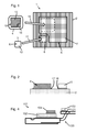
- FIG. 1 shows a multiple die arrangement 1 comprising a first, base die 2 , a second die 3 and a third die 4 .
- the base die 2 includes a semiconductor device comprising a triac 5 .
- An upper surface of the triac includes a gate terminal 6 and a first anode 7 .
- the second die 3 includes a semiconductor device comprising a diode 8 having an anode terminal on its lower surface (not visible) and a cathode terminal 10 on its upper surface.
- the second die 3 is configured to be stacked on the base die 2 .
- the anode terminal of the diode 8 is configured to be stacked on and electrically connected to the gate terminal 6 of the triac 5 , as shown by the dashed outline and arrow 11 .
- the third die 4 includes a semiconductor device comprising a thyristor 12 having a first anode terminal on its lower surface (not visible) and a second anode terminal 13 on its upper surface alongside a gate terminal 14 .
- the third die 4 is configured to be stacked on the base die 2 in the same plane as the second die 3 .
- the first anode of the thyristor 12 is configured to be stacked on and electrically connected to the first anode 7 of the triac 5 , as shown by the dashed outline and arrow 15 .
- FIG. 2 shows a side view of the arrangement 1 with the second die 3 of the diode 8 and the third die 4 of the thyristor 12 mounted in a stacked configuration on the base die 2 .
- the second and third dies lie in the same plane.
- the second die 3 and base die are secured together by a conductive die attach material 16 .
- the die attach material provides the electrical connection between the anode terminal of the diode and the gate terminal 6 of the triac 5 .
- the third die 4 and base die are secured together by a conductive die attach material 17 .
- the die attach material 17 provides the electrical connection between the first anode terminal of the thyristor 12 and the first anode terminal 7 of the triac 5 . Incorrect placement or spreading of the die attach material 16 , 17 can lead to misplaced connections.
- FIG. 3 shows an alternative arrangement 101 of the multiple die arrangement.
- the same reference numerals have been used for like parts but with the addition of “100” to the number used in FIGS. 1 and 2 .
- FIG. 4 shows a side view of the embodiment of FIG. 3 .
- a lead frame 120 is shown mounted to the base die 102 .
- the lead frame includes lead fingers for providing an external electrical connection to the die arrangement 101 .
- the lead frame includes three lead fingers; a first lead finger 121 , a second lead finger 122 and a third lead linger 123 .
- the lead fingers provide for connection of the terminals of the semiconductor devices on the dies 102 , 103 , 104 to circuitry external to the arrangement 101 .
- the first and third lead fingers 121 and 123 are substantially T-shaped (although could be L-shaped) and include a wider, head portion 124 and 125 respectively adjacent the base die 101 and a narrower portion 126 , 127 .
- the wider portions 124 , 125 may be configured to be encapsulated within a package and the narrower portions 126 , 127 may extend from the package.
- the second die 103 is mounted on the lead finger 121 and, in particular, the wider portion 124 thereof.
- the second die may be attached by conductive die attach material, such as solder.
- the wider portion of a lead finger, where it meets the remainder of the leadframe, is an advantageous point to mount a die.
- a bondwire 125 connects the second die 103 to the gate terminal 106 of the triac 105 of the base die 102 .
- the second die 103 is mounted the opposite way up.
- the anode terminal 129 of the diode 110 is mounted facing upwards from the lead finger such that an electrical connection can be formed between it and the gate terminal 106 .
- the second die 103 may be provided with the reverse N-type and P-type diffusion arrangement compared to that provided in the example of FIG. 1 .
- the diode had a lower P-type diffusion and an upper N-type diffusion (such that the P-type diffusion formed the anode terminal which contacted the gate terminal 6 of the triac 5 )
- the arrangement 101 has a upper P-type diffusion and a lower N-type diffusion, such that a bondwire can connect the P-type diffusion region to the gate terminal 6 .
- the third die 104 is stacked on the base die 2 as in the example of FIG. 1 and secured by die attach material or solder for example.
- a second bondwire 128 electrically connects the second anode terminal 13 of the thyristor 12 of third die 104 to the first lead finger 121 .
- a third bondwire 130 connects the first anode 107 of the triac 105 to the third lead finger 123 .
- the arrangement 101 may comprise a temperature and overload protected Triac.
- a diode as comprising an electronic device, formed in a die, suitable for lead finger mounting.
- other devices may be lead finger mounted.
- two or more terminal devices wherein two of the terminals are formed on opposite sides of the die are suitable.
- dies having all terminals on one side may be mounted to the lead finger by their non-terminal side.
- FIG. 5 shows a further example of a die arrangement 201 .
- the arrangement comprises a first die 202 and a second die 203 .
- the first die 202 includes a semiconductor device formed therein having, for example, two terminals on its upper surface; a first terminal 206 and a second terminal 207 .
- the first die 202 is itself stacked upon a base die (not visible) which is mounted to a lead frame 220 .
- the lead frame includes three lead fingers; a first lead finger 221 , a second lead finger 222 and a third lead linger 223 .
- the lead fingers provide for connection of the terminals of the semiconductor devices on the dies 202 , 203 to circuitry external to the arrangement 201 .
- the second die 203 is mounted to one of the lead fingers 221 and a bondwire 225 electrically connects the semiconductor device of the second die 203 to one of the terminals 206 , 207 of the first die 202 .
- the die 203 has been mounted on the lead finger 221 .
- the second terminal 207 to which the second die is electrically connected has an area smaller than the second die 203 . Thus, it is more convenient to mount the second die to the lead finger 221 .
- a further bondwire 228 connects the first terminal 206 of the first die 202 to the third lead finger 223 .
Landscapes
- Lead Frames For Integrated Circuits (AREA)
- Engineering & Computer Science (AREA)
- Microelectronics & Electronic Packaging (AREA)
Abstract
Description
-
- a first die including at least one semiconductor device;
- a second die including at least one semiconductor device;
- a lead frame associated with the first die and comprising one or more lead fingers,
- wherein the second die is mounted on the or one of the lead fingers and electrically connected to a further element by a bond wire.
-
- receiving a first die including at least one semiconductor device;
- receiving a second die including at least one semiconductor device;
- mounting the first die to a lead frame, the lead frame comprising one or more lead fingers,
- mounting the second die on one of the lead fingers; and
- electrically connecting the semiconductor device of the second die to a further element by a bond wire.
-
- the step of electrically connecting comprises electrically connecting the semiconductor device of the second die to the smaller, first terminal of the first die by a bond wire; and
- the method include the step of mounting a third die on the second, larger area, terminal of the first die in a stacked configuration.
Claims (14)
Applications Claiming Priority (3)
| Application Number | Priority Date | Filing Date | Title |
|---|---|---|---|
| EP14192543.8A EP3018710B1 (en) | 2014-11-10 | 2014-11-10 | Arrangement of semiconductor dies |
| EP14192543.8 | 2014-11-10 | ||
| EP14192543 | 2014-11-10 |
Publications (2)
| Publication Number | Publication Date |
|---|---|
| US20160133547A1 US20160133547A1 (en) | 2016-05-12 |
| US9685396B2 true US9685396B2 (en) | 2017-06-20 |
Family
ID=51893882
Family Applications (1)
| Application Number | Title | Priority Date | Filing Date |
|---|---|---|---|
| US14/865,985 Active US9685396B2 (en) | 2014-11-10 | 2015-09-25 | Semiconductor die arrangement |
Country Status (2)
| Country | Link |
|---|---|
| US (1) | US9685396B2 (en) |
| EP (1) | EP3018710B1 (en) |
Cited By (1)
| Publication number | Priority date | Publication date | Assignee | Title |
|---|---|---|---|---|
| US11515238B2 (en) | 2019-06-27 | 2022-11-29 | Nxp Usa, Inc. | Power die package |
Families Citing this family (2)
| Publication number | Priority date | Publication date | Assignee | Title |
|---|---|---|---|---|
| US9716057B1 (en) * | 2016-08-24 | 2017-07-25 | United Silicon Carbide, Inc. | Offset leadframe cascode package |
| US11037915B2 (en) * | 2019-02-14 | 2021-06-15 | Facebook Technologies, Llc | Integrated display devices |
Citations (21)
| Publication number | Priority date | Publication date | Assignee | Title |
|---|---|---|---|---|
| US4914045A (en) * | 1985-12-19 | 1990-04-03 | Teccor Electronics, Inc. | Method of fabricating packaged TRIAC and trigger switch |
| JPH06342818A (en) | 1993-06-02 | 1994-12-13 | Hitachi Ltd | Semiconductor device |
| US6055148A (en) * | 1997-07-19 | 2000-04-25 | U.S. Philips Corporation | Semiconductor device assemblies and circuits |
| US6184585B1 (en) * | 1997-11-13 | 2001-02-06 | International Rectifier Corp. | Co-packaged MOS-gated device and control integrated circuit |
| DE10303932A1 (en) | 2002-09-05 | 2004-03-25 | Infineon Technologies Ag | Electronic power module, comprises at least two semiconductor chips arranged in stack on substrate carrier, at least one chip being a silicon-carbide power semiconductor device |
| US20090127685A1 (en) * | 2007-11-21 | 2009-05-21 | Jong Man-Kyo | Power Device Packages and Methods of Fabricating the Same |
| US20110100681A1 (en) * | 2008-04-28 | 2011-05-05 | Peter Kimmich | Substrate-mounted circuit module having components in a plurality of contacting planes |
| US20110169144A1 (en) * | 2010-01-13 | 2011-07-14 | Tomas Moreno | Die package including multiple dies and lead orientation |
| US20110220916A1 (en) | 2010-03-12 | 2011-09-15 | Renesas Electronics Corporation | Electronic circuit device |
| US8022522B1 (en) * | 2005-04-01 | 2011-09-20 | Marvell International Ltd. | Semiconductor package |
| US20120228696A1 (en) * | 2011-03-07 | 2012-09-13 | Texas Instruments Incorporated | Stacked die power converter |
| US8299588B1 (en) * | 2011-07-07 | 2012-10-30 | Texas Instruments Incorporated | Structure and method for uniform current distribution in power supply module |
| US20130049137A1 (en) * | 2011-08-26 | 2013-02-28 | Renesas Electronics Corporation | Semiconductor device |
| US20130069210A1 (en) * | 2011-09-16 | 2013-03-21 | Samsung Electro-Mechanics Co., Ltd. | Power module package |
| US8471373B2 (en) * | 2010-06-11 | 2013-06-25 | Panasonic Corporation | Resin-sealed semiconductor device and method for fabricating the same |
| CN203707109U (en) | 2014-01-20 | 2014-07-09 | 深圳市鹏微科技有限公司 | Multi-integration triode |
| US20150084173A1 (en) * | 2013-09-25 | 2015-03-26 | Mitsubishi Electric Corporation | Semiconductor device and method of manufacturing the same |
| US20150173246A1 (en) * | 2013-12-18 | 2015-06-18 | Samsung Electro-Mechanics Co., Ltd. | Power module package and method for manufacturing the same |
| US20150187726A1 (en) * | 2013-12-31 | 2015-07-02 | Samsung Electro-Mechanics Co., Ltd. | Semiconductor package and method for manufacturing the same |
| US20150311144A1 (en) * | 2013-03-09 | 2015-10-29 | Adventive Ipbank | Low-Profile Footed Power Package |
| US20160268241A1 (en) * | 2013-09-12 | 2016-09-15 | Kabushiki Kaisha Toshiba | Semiconductor device having a mounting member that includes a die pad unit and terminals with multiple conductive regions |
-
2014
- 2014-11-10 EP EP14192543.8A patent/EP3018710B1/en active Active
-
2015
- 2015-09-25 US US14/865,985 patent/US9685396B2/en active Active
Patent Citations (21)
| Publication number | Priority date | Publication date | Assignee | Title |
|---|---|---|---|---|
| US4914045A (en) * | 1985-12-19 | 1990-04-03 | Teccor Electronics, Inc. | Method of fabricating packaged TRIAC and trigger switch |
| JPH06342818A (en) | 1993-06-02 | 1994-12-13 | Hitachi Ltd | Semiconductor device |
| US6055148A (en) * | 1997-07-19 | 2000-04-25 | U.S. Philips Corporation | Semiconductor device assemblies and circuits |
| US6184585B1 (en) * | 1997-11-13 | 2001-02-06 | International Rectifier Corp. | Co-packaged MOS-gated device and control integrated circuit |
| DE10303932A1 (en) | 2002-09-05 | 2004-03-25 | Infineon Technologies Ag | Electronic power module, comprises at least two semiconductor chips arranged in stack on substrate carrier, at least one chip being a silicon-carbide power semiconductor device |
| US8022522B1 (en) * | 2005-04-01 | 2011-09-20 | Marvell International Ltd. | Semiconductor package |
| US20090127685A1 (en) * | 2007-11-21 | 2009-05-21 | Jong Man-Kyo | Power Device Packages and Methods of Fabricating the Same |
| US20110100681A1 (en) * | 2008-04-28 | 2011-05-05 | Peter Kimmich | Substrate-mounted circuit module having components in a plurality of contacting planes |
| US20110169144A1 (en) * | 2010-01-13 | 2011-07-14 | Tomas Moreno | Die package including multiple dies and lead orientation |
| US20110220916A1 (en) | 2010-03-12 | 2011-09-15 | Renesas Electronics Corporation | Electronic circuit device |
| US8471373B2 (en) * | 2010-06-11 | 2013-06-25 | Panasonic Corporation | Resin-sealed semiconductor device and method for fabricating the same |
| US20120228696A1 (en) * | 2011-03-07 | 2012-09-13 | Texas Instruments Incorporated | Stacked die power converter |
| US8299588B1 (en) * | 2011-07-07 | 2012-10-30 | Texas Instruments Incorporated | Structure and method for uniform current distribution in power supply module |
| US20130049137A1 (en) * | 2011-08-26 | 2013-02-28 | Renesas Electronics Corporation | Semiconductor device |
| US20130069210A1 (en) * | 2011-09-16 | 2013-03-21 | Samsung Electro-Mechanics Co., Ltd. | Power module package |
| US20150311144A1 (en) * | 2013-03-09 | 2015-10-29 | Adventive Ipbank | Low-Profile Footed Power Package |
| US20160268241A1 (en) * | 2013-09-12 | 2016-09-15 | Kabushiki Kaisha Toshiba | Semiconductor device having a mounting member that includes a die pad unit and terminals with multiple conductive regions |
| US20150084173A1 (en) * | 2013-09-25 | 2015-03-26 | Mitsubishi Electric Corporation | Semiconductor device and method of manufacturing the same |
| US20150173246A1 (en) * | 2013-12-18 | 2015-06-18 | Samsung Electro-Mechanics Co., Ltd. | Power module package and method for manufacturing the same |
| US20150187726A1 (en) * | 2013-12-31 | 2015-07-02 | Samsung Electro-Mechanics Co., Ltd. | Semiconductor package and method for manufacturing the same |
| CN203707109U (en) | 2014-01-20 | 2014-07-09 | 深圳市鹏微科技有限公司 | Multi-integration triode |
Non-Patent Citations (1)
| Title |
|---|
| Extended European Search Report for EP Patent Appln. No. 14192543.8 (May 13, 2015). |
Cited By (1)
| Publication number | Priority date | Publication date | Assignee | Title |
|---|---|---|---|---|
| US11515238B2 (en) | 2019-06-27 | 2022-11-29 | Nxp Usa, Inc. | Power die package |
Also Published As
| Publication number | Publication date |
|---|---|
| US20160133547A1 (en) | 2016-05-12 |
| EP3018710A1 (en) | 2016-05-11 |
| EP3018710B1 (en) | 2020-08-05 |
Similar Documents
| Publication | Publication Date | Title |
|---|---|---|
| CN205789962U (en) | Circuit and packaged type electronic equipment | |
| US9905500B2 (en) | Semiconductor component and method of manufacture | |
| US9171774B2 (en) | Power semiconductor module and method of manufacturing the same | |
| US9196577B2 (en) | Semiconductor packaging arrangement | |
| US20100176508A1 (en) | Semiconductor device package and method of assembly thereof | |
| JP6892261B2 (en) | LED package | |
| US10770381B2 (en) | Semiconductor component and method of manufacture | |
| JP5924110B2 (en) | Semiconductor device, semiconductor device module, and semiconductor device manufacturing method | |
| US8901721B1 (en) | Lead frame based semiconductor die package | |
| US20070045785A1 (en) | Reversible-multiple footprint package and method of manufacturing | |
| US11094681B2 (en) | Photocoupler and packaging member thereof | |
| US9735095B2 (en) | Semiconductor component and method of manufacture | |
| US20140210061A1 (en) | Chip arrangement and chip package | |
| US9620443B2 (en) | Semiconductor component and method of manufacture | |
| US9991183B2 (en) | Semiconductor component having inner and outer semiconductor component housings | |
| CN103824853A (en) | Integrated circuit module applied to switch type regulator | |
| US10529644B2 (en) | Semiconductor device | |
| CN107546191A (en) | Semiconductor power device with single row direct insert leadthrough module and preparation method thereof | |
| US9685396B2 (en) | Semiconductor die arrangement | |
| US9373566B2 (en) | High power electronic component with multiple leadframes | |
| KR101983165B1 (en) | Semiconductor package | |
| US9153518B2 (en) | Molded semiconductor package with pluggable lead | |
| KR102283390B1 (en) | Semiconductor package for multi chip and method of fabricating the same | |
| KR20160059451A (en) | Package structure and method of manufacture thereof, and carrier | |
| KR20150142916A (en) | Semiconductor package and method for manufacturing the same |
Legal Events
| Date | Code | Title | Description |
|---|---|---|---|
| AS | Assignment |
Owner name: NXP B.V., NETHERLANDS Free format text: ASSIGNMENT OF ASSIGNORS INTEREST;ASSIGNOR:NAVAJA, DEOREX DAVID AVILA;REEL/FRAME:036660/0702 Effective date: 20150923 |
|
| STCF | Information on status: patent grant |
Free format text: PATENTED CASE |
|
| MAFP | Maintenance fee payment |
Free format text: PAYMENT OF MAINTENANCE FEE, 4TH YEAR, LARGE ENTITY (ORIGINAL EVENT CODE: M1551); ENTITY STATUS OF PATENT OWNER: LARGE ENTITY Year of fee payment: 4 |
|
| MAFP | Maintenance fee payment |
Free format text: PAYMENT OF MAINTENANCE FEE, 8TH YEAR, LARGE ENTITY (ORIGINAL EVENT CODE: M1552); ENTITY STATUS OF PATENT OWNER: LARGE ENTITY Year of fee payment: 8 |