US8884650B2 - High-frequency semiconductor switching circuit - Google Patents
High-frequency semiconductor switching circuit Download PDFInfo
- Publication number
- US8884650B2 US8884650B2 US13/741,999 US201313741999A US8884650B2 US 8884650 B2 US8884650 B2 US 8884650B2 US 201313741999 A US201313741999 A US 201313741999A US 8884650 B2 US8884650 B2 US 8884650B2
- Authority
- US
- United States
- Prior art keywords
- control
- path switching
- fet stages
- shunt
- stages
- Prior art date
- Legal status (The legal status is an assumption and is not a legal conclusion. Google has not performed a legal analysis and makes no representation as to the accuracy of the status listed.)
- Active, expires
Links
Images


Classifications
-
- H—ELECTRICITY
- H03—ELECTRONIC CIRCUITRY
- H03K—PULSE TECHNIQUE
- H03K19/00—Logic circuits, i.e. having at least two inputs acting on one output; Inverting circuits
- H03K19/0008—Arrangements for reducing power consumption
- H03K19/0013—Arrangements for reducing power consumption in field effect transistor circuits
-
- H—ELECTRICITY
- H03—ELECTRONIC CIRCUITRY
- H03K—PULSE TECHNIQUE
- H03K17/00—Electronic switching or gating, i.e. not by contact-making and –breaking
- H03K17/51—Electronic switching or gating, i.e. not by contact-making and –breaking characterised by the components used
- H03K17/56—Electronic switching or gating, i.e. not by contact-making and –breaking characterised by the components used by the use, as active elements, of semiconductor devices
- H03K17/567—Circuits characterised by the use of more than one type of semiconductor device, e.g. BIMOS, composite devices such as IGBT
-
- H—ELECTRICITY
- H03—ELECTRONIC CIRCUITRY
- H03K—PULSE TECHNIQUE
- H03K17/00—Electronic switching or gating, i.e. not by contact-making and –breaking
- H03K17/51—Electronic switching or gating, i.e. not by contact-making and –breaking characterised by the components used
- H03K17/74—Electronic switching or gating, i.e. not by contact-making and –breaking characterised by the components used by the use, as active elements, of diodes
- H03K17/76—Switching arrangements with several input- or output-terminals, e.g. multiplexers, distributors
Definitions
- the present invention relates to a high-frequency semiconductor switching circuit.
- high-frequency semiconductor switching circuits which are small in size and low in power consumption are required to switch high-frequency signal transmission paths, such as to switch the transmission and reception with respect to an antenna.
- a high-frequency semiconductor switching circuit including as a switching element a GaAsFET (Gallium Arsenide Field Effect Transistor) which excels in a high frequency property and low power consumption has been used.
- a semiconductor substrate as represented by a SOS (Silicon On Sapphire) substrate or a SOI (Silicon On Insulator) substrate, produced by the combination of a substrate material having an excellent insulation property and a silicon process has been improved.
- a technology of adopting a MOSFET (Metal Oxide Semiconductor Field Effect Transistor) as a switching element for path switching has been developed although the MOSFET has been unfavorable for use in the high-frequency semiconductor switching circuit.
- the MOSFET can be caused to become a conducting state by applying a high-level voltage (for example, 3 V), adequately higher than a pinch-off voltage, as a gate bias voltage to create a low impedance between a drain and a source.
- the MOSFET can be caused to become a cutoff state by applying a low-level voltage (for example, 0 V), adequately lower than the pinch-off voltage, as the gate bias voltage to create a high impedance between the drain and the source.
- FIG. 14 is a circuit diagram showing Configuration Example 1 of a conventional high-frequency semiconductor switching circuit as shown in FIG. 13 of Japanese Patent No. 4105183.
- the high-frequency semiconductor switching circuit of FIG. 14 is, for example, a high-frequency SP3T (Single-Pole Triple-Throw) switch used as, for example, an antenna switch configured to switch output paths for an input high-frequency signal.
- the high-frequency semiconductor switching circuit of FIG. 14 includes a common input-output terminal 1101 and individual input-output terminals 1102 , 1103 , and 1104 .
- a path switching FET stage 1108 configured to perform switching of high-frequency signal paths is connected between the common input-output terminal 1101 and the individual input-output terminal 1102 .
- a path switching FET stage 1109 configured to perform the switching of the high-frequency signal paths is connected between the common input-output terminal 1101 and the individual input-output terminal 1103 .
- a path switching FET stage 1110 configured to perform the switching of the high-frequency signal paths is connected between the common input-output terminal 1101 and the individual input-output terminal 1104 .
- Each of the path switching FET stages 1108 , 1109 , and 1110 is constituted by MESFETs (Metal-Semiconductor Field Effect Transistors) of a GaAs material and has a structure in which a metal of a schottky junction type is formed as a gate on a semiconductor substrate.
- MESFETs Metal-Semiconductor Field Effect Transistors
- Gates of the MESFETs constituting the path switching FET stage 1108 are connected to a control terminal 1105 through a gate bias resistor 1111 .
- gates of the MESFETs constituting the path switching FET stage 1109 are connected to a control terminal 1106 through a gate bias resistor 1112 .
- gates of the MESFETs constituting the path switching FET stage 1110 are connected to a control terminal 1107 through a gate bias resistor 1113 .
- the path switching FET stages 1108 , 1109 , and 1110 are caused to become the conducting state or the cutoff state.
- the common input-output terminal 1101 is electrically connected to at least one of the individual input-output terminals 1102 , 1103 , and 1104 .
- a high-frequency semiconductor switching circuit is constituted only by path switching FETs, such as the MESFETs of Conventional Configuration Example 1, there is a problem of achieving both low insertion loss and high isolation.
- path switching FETs such as the MESFETs of Conventional Configuration Example 1
- a gate width may be reduced in order to obtain the high isolation.
- an on resistance increases by reducing the gate width, the insertion loss deteriorates.
- FIG. 15 is a circuit diagram showing Configuration Example 2 of the conventional high-frequency semiconductor switching circuit as shown in FIG. 14 of Japanese Patent No. 4105183.
- the high-frequency semiconductor switching circuit of FIG. 15 is a high-frequency SP3T switch configured such that path switching FET stages and shunt FET stages for securing the isolation are combined on high-frequency signal paths.
- the path switching FET stages and the shunt FET stages as above, the high-frequency signal leaking through capacitor components of the path switching FETs of the cutoff state can be caused to be sent to ground by the shunt FETs of the conducting state.
- the high isolation can be obtained.
- the problem of Conventional Configuration Example 1 is solved.
- a shunt FET stage 1214 is provided between an individual input-output terminal 1202 and the ground.
- a state between a common input-output terminal 1201 and the individual input-output terminal 1202 is the cutoff state, the signal leaking from the common input-output terminal 1201 through a path switching FET stage 1211 to the individual input-output terminal 1202 is sent to the ground.
- a shunt FET stage 1215 is provided between an individual input-output terminal 1203 and the ground.
- a shunt FET stage 1216 is provided between an individual input-output terminal 1204 and the ground.
- a shunt circuit is constituted by the shunt FET stages 1214 , 1215 , and 1216 .
- Resistor groups 1220 , 1221 , and 1222 denote resistors respectively connected to the gates of the FETs of the shunt FET stages 1214 , 1215 , and 1216 .
- DC cut capacitors 1223 , 1224 , and 1225 denote DC cut capacitors respectively connected to the shunt FET stages 1214 , 1215 , and 1216 in series.
- control terminals 1205 to 1210 By respectively applying control voltages to control terminals 1205 to 1210 , three path switching FET stages 1211 to 1213 and three shunt PET stages 1214 to 1216 are caused to become the conducting state or the cutoff state. Specifically, as shown by a truth table of FIG. 16 , when the control terminal 1205 becomes the high level, the control terminal 1208 becomes the low level. Similarly, when the control terminal 1206 becomes the high level, the control terminal 1209 becomes the low level. Further, when the control terminal 1208 becomes the high level, the control terminal 1210 becomes the low level. With this, the isolation property between the high-frequency signals is satisfactorily maintained. Two or more out of the control terminals 1205 to 1207 may become the high level at the same time.
- FIG. 17 is a circuit diagram showing Configuration Example 3 of the conventional high-frequency semiconductor switching circuit as shown in FIG. 3 of Japanese Laid-Open Patent Application Publication No. 6-85641.
- one example of the easiest method of avoiding the increase in the number of control terminals is a method of respectively inserting inverter circuits 1326 to 1328 in control terminals 1305 to 1307 .
- the inverter circuit is a circuit configured to invert an input voltage to generate an output voltage. When a high-level input voltage is applied to the inverter circuit, the inverter circuit generates a low-level output voltage.
- the inverter circuit When a low-level input voltage is applied to the inverter circuit, the inverter circuit generates a high-level output voltage.
- an input port of the inverter circuit 1326 is connected to the control terminal 1305 , and an output port thereof is connected through a resistor group 1320 to respective gates of a shunt FET stage 1314 .
- an input port of the inverter circuit 1327 is connected to the control terminal 1306 , and an output port thereof is connected through a resistor group 1321 to respective gates of a shunt FET stage 1315 .
- an input port of the inverter circuit 1328 is connected to the control terminal 1307 , and an output port thereof is connected through a resistor group 1322 to respective gates of a shunt FET stage 1316 .
- Power supply ports of the inverter circuits 1326 to 1328 are connected to a power supply terminal 1308 .
- the same operations as the high-frequency semiconductor switching circuit shown in FIG. 15 are performed only by the control terminals 1305 , 1306 , and 1307 .
- the shunt FET stage 1314 becomes the cutoff state.
- the shunt FET stage 1315 becomes the cutoff state.
- the shunt FET stage 1316 becomes the cutoff state.
- FIG. 19 is a circuit diagram showing Configuration Example 4 of the conventional high-frequency semiconductor switching circuit as shown in FIG. 1 of Japanese Patent No. 4105183.
- Configuration Example 4 of the conventional high-frequency semiconductor switching circuit as shown in FIG. 1 of Japanese Patent No. 4105183.
- one example of the easiest method of avoiding the increase in the number of control terminals and the addition of the power supply terminal as in Conventional Configuration Example 3 is a method of inserting a diode logic circuit to each of control terminals 1405 to 1407 .
- the diode logic circuit is constituted by a plurality of diodes formed as metal-semiconductor schottky junctions on a compound semiconductor substrate.
- diodes 1426 to 1431 are diodes constituting a diode logic circuit OR 1 and are produced as the metal-semiconductor schottky junctions by using the same material as a gate electrode of a metal-semiconductor FET. This diode can be produced in a FET production process at the same time as the FET.
- An anode of the diode 1426 is connected to the control terminal 1407 , and a cathode thereof is connected to respective gates of a shunt FET stage 1414 and also connected through a resistor 1432 to ground.
- An anode of the diode 1427 is connected to the control terminal 1406 , and a cathode thereof is connected to the cathode of the diode 1426 .
- An anode of the diode 1428 is connected to the control terminal 1407 , and a cathode thereof is connected to respective gates of a shunt FET stage 1415 and also connected through a resistor 1433 to the ground.
- An anode of the diode 1429 is connected to the control terminal 1405 , and a cathode thereof is connected to the cathode of the diode 1428 .
- An anode of the diode 1430 is connected to the control terminal 1406 , and a cathode thereof is connected to respective gates of a shunt FET stage 1416 and also connected through a resistor 1434 to the ground.
- An anode of the diode 1431 is connected to the control terminal 1405 , and a cathode thereof is connected to the cathode of the diode 1430 .
- the same operations as the high-frequency semiconductor switching circuits shown in FIGS. 15 and 17 are performed only by three control terminals 1405 to 1407 without providing a common power supply terminal. Specifically, when a path switching FET stage 1411 becomes the conducting state, the shunt FET stage 1414 becomes the cutoff state. Similarly, when a path switching FET stage 1412 becomes the conducting state, the shunt FET stage 1415 becomes the cutoff state. When a path switching FET stage 1413 becomes the conducting state, the shunt FET stage 1416 becomes the cutoff state. With this, the isolation property between the high-frequency signals is satisfactorily maintained.
- the path switching FET stage 1411 and the shunt FET stage 1414 become the conducting state at the same time. Therefore, the deterioration of the insertion loss occurs, and the path switching FET stage 1411 does not normally become the conducting state as a switch.
- the path switching FET stage 1412 and the shunt FET stage 1415 become the conducting state at the same time, the deterioration of the insertion loss occurs, and the path switching FET stage 1412 does not normally become the conducting state as a switch.
- the present invention was made to solve the above problems, and an object of the present invention is to provide a high-function high-frequency switching circuit capable of causing two or more path switching FET stages to become the conducting state at the same time while maintaining satisfactory properties, such as low insertion loss, high isolation, and low strain and realizing size reduction and low power consumption without adding a power supply terminal.
- a high-frequency semiconductor switching circuit includes: a semiconductor substrate; one common input-output terminal, three or more individual input-output terminals, and three or more control terminals corresponding to the three or more individual input-output terminals, these terminals being formed on the semiconductor substrate; three or more path switching FET stages formed on the semiconductor substrate and each provided between the common input-output terminal and a corresponding one of the three or more individual input-output terminals; one or more shunt FET stages formed on the semiconductor substrate and each provided between ground and at least one of the three or more individual input-output terminals; and a diode-switch logic circuit including diodes and switches formed on the semiconductor substrate such that a group of a part of the diodes and a part of the switches corresponds to each of the one or more shunt FET stages, the diode-switch logic circuit being configured to control the three or more path switching FET stages and the one or more shunt FET stages, where
- each of the switches may be an inversion control switch configured to be turned off when the control voltage to be applied to the gate is a high level and turned on when the control voltage to be applied to the gate is a low level, cathode sides of the diodes respectively connected to the remaining control terminals may be short-circuited, a ground resistor may be connected between ground and a short-circuit point where the cathode sides of the diodes respectively connected to the remaining control terminals are short-circuited, and a
- the diode-switch logic circuit performs the logic synthesis of three or more control voltages respectively input to three or more control terminals.
- one or more shunt FET stages for securing the isolation can be controlled based on three or more control voltages respectively applied to the gates of three or more path switching FET stages.
- the gate voltage(s) of one or more shunt FET stages can be prepared by utilizing the control voltages respectively applied to the gates of three or more path switching FET stages, a power supply circuit including a power supply terminal and its wire are unnecessary.
- the high-frequency semiconductor switching circuit can be reduced in size, and therefore, a mobile communication device including the high-frequency semiconductor switching circuit can be reduced in size, and the power consumption can be reduced. Further, unlike Conventional Configuration Example 4, two or more path switching FET stages can be caused to become the conducting state at the same time. Thus, the high-function high-frequency switching circuit can be realized.
- the above high-frequency semiconductor switching circuit may further includes: first short circuit resistors each connected between a source and drain of a corresponding one of the three or more path switching FET stages; second short circuit resistors each connected between a source and drain of a corresponding one of the one or more shunt FET stages; first DC cut capacitors respectively provided at drain sides and source sides of the three or more path switching FET stages; and second DC cut capacitors respectively provided at drain sides and source sides of the one or more shunt FET stages, wherein: the short-circuit points at each of which the cathode sides of the diodes are short-circuited may be each connected through a corresponding one of the first short circuit resistors to the drain side of a corresponding one of the three or more path switching FET stages; and the three or more control terminals may be each connected through a corresponding one of the second short circuit resistors to the drain side of a corresponding one of the one or more shunt FET stages.
- the present invention can provide the high-frequency semiconductor switching circuit having the above effects, capable of causing the path switching FET stages to surely become the conducting state or the cutoff state and suppressing the leakage to the high-frequency signal path of the cutoff state, and including satisfactory properties, such as high isolation and low strain. Further, without adding a dedicated power supply terminal, the source voltages and drain voltages of the path switching FET stages can be fixed. Therefore, the high-frequency semiconductor switching circuit can be reduced in size, and therefore, the mobile communication device including the high-frequency semiconductor switching circuit can be reduced in size, and the power consumption can be reduced.
- each of the three or more path switching FET stages may be configured by connecting a plurality of path switching FETs in series
- each of the one or more shunt FET stages may be configured by connecting a plurality of shunt FETs in series
- a part of the path switching FETs constituting at least two out of the three or more path switching FET stages may be integrated.
- a part of reception-side FET stages configured to handle low electric power can be integrated, and the integrated FET stage can be controlled by the diode-switch logic circuit.
- the semiconductor substrate may be a SOI substrate or a SOS substrate.
- the high-frequency semiconductor switching circuit can be provided by using the FETs formed on the SOS substrate or SOI substrate, which is high in specific resistance and does not require the application of the bias of the back gate.
- the diodes can be formed on the SOS substrate or SOI substrate by utilizing a general MOSFET production process.
- the diodes may be PN junction diodes formed on the semiconductor substrate, anode sides of the diodes may be respectively connected to the control terminals, and cathode sides of the diodes may be respectively connected to the switches.
- the PN junction diodes can be formed on the SOS substrate or SOI substrate by utilizing the general MOSFET production process.
- the diodes may be diode-connected NMOSFETs, drains of the diodes may be respectively connected to the control terminals, sources of the diodes may be respectively connected to the switches, and gates of the diodes may be respectively connected to the drains of the diodes.
- the NMOSFET can operate in the same manner as a general diode by connecting (diode-connecting) the gate and drain thereof.
- the forward voltage In the case of a PN junction diode formed on a silicon substrate, the forward voltage of about 0.6 V is generated for each diode.
- the forward voltage can be controlled by adjusting the gate length, gate width, and pinch-off voltage of the NMOSFET. For example, in the NMOSFET in which the gate length is 0.25 ⁇ m, and the pinch-off voltage is 0.3 V, the forward voltage becomes 0.3 V to 0.6 V. Therefore, the voltage drop of the NMOSFET can be made smaller than that of the PN junction diode. As a result, the gate voltage applied to the gate electrode of each shunt FET stage can be set high, which is effective for the isolation property.
- the switches may be PMOSFETs, sources of the switches may be respectively connected to cathode sides of the diodes, drains of the switches may be respectively connected to the short circuit resistors, and gates of the switches may be respectively connected to the control terminals.
- the gate voltage when the gate voltage is the high level, the gate voltage becomes adequately lower than the pinch-off voltage, and the PMOSFET becomes the cutoff state.
- the gate voltage When the gate voltage is the low level, the gate voltage becomes adequately higher than the pinch-off voltage, and the PMOSFET becomes the conducting state. Therefore, the calculation result of the logical negation (NOT) of the control voltage can be output.
- NOT logical negation
- a body potential needs to be connected to the highest potential, such as a power supply terminal, in a circuit to prevent latch-up.
- the diode-switch logic circuit can be easily produced without providing an additional power supply terminal to prevent the latch-up.
- each of the three or more path switching FET stages may be configured by connecting a plurality of MOSFETs in series.
- the withstand voltage in the case of handling the high-frequency signal of high electric power on the high-frequency signal path can be increased.
- each of the one or more shunt FET stages may be configured by connecting a plurality of MOSFETs in series.
- the withstand voltage in the case of handling the high-frequency signal of high electric power on the high-frequency signal path can be increased.
- the high-function high-frequency switching circuit capable of causing two or more path switching FET stages to become the conducting state at the same time can be realized while maintaining satisfactory properties, such as low insertion loss, high isolation, and low strain and realizing the size reduction and the low power consumption without adding a power supply terminal.
- FIG. 1 is a circuit diagram showing a configuration example of a high-frequency semiconductor switching circuit according to Embodiment 1 of the present invention.
- FIG. 2 is a control logic table of a diode-switch logic circuit of FIG. 1 .
- FIG. 3B is a plan view showing one example of the diode of FIG. 3A .
- FIG. 3C is a cross-sectional view showing one example of the diode of FIG. 3A .
- FIG. 5 is a circuit diagram showing Modification Example 1 of the high-frequency semiconductor switching circuit according to Embodiment 1 of the present invention.
- FIG. 6 is a circuit diagram showing Modification Example 2 of the high-frequency semiconductor switching circuit according to Embodiment 1 of the present invention.
- FIG. 7 is a circuit diagram showing Modification Example 3 of the high-frequency semiconductor switching circuit according to Embodiment 1 of the present invention.
- FIG. 8 is a circuit diagram showing Modification Example 4 of the high-frequency semiconductor switching circuit according to Embodiment 1 of the present invention.
- FIG. 9 is a circuit diagram showing Modification Example 5 of the high-frequency semiconductor switching circuit according to Embodiment 1 of the present invention.
- FIG. 10 is a circuit diagram showing Modification Example 6 of the high-frequency semiconductor switching circuit according to Embodiment 1 of the present invention.
- FIG. 11 is a circuit diagram showing a configuration example of the high-frequency semiconductor switching circuit according to Embodiment 2 of the present invention.
- FIG. 12 is a schematic diagram showing a configuration example of a mobile communication device including the high-frequency semiconductor switching circuit according to Embodiment 3 of the present invention.
- FIG. 13 is a circuit diagram showing a configuration example of the high-frequency semiconductor switching circuit according to Embodiment 3 of the present invention.
- FIG. 14 is a circuit diagram showing Configuration Example 1 of a conventional high frequency semiconductor switching circuit.
- FIG. 15 is a circuit diagram showing Configuration Example 2 of the conventional high-frequency semiconductor switching circuit as shown in FIG. 14 of Japanese Patent No. 4105183.
- FIG. 16 is a truth table of the high-frequency semiconductor switching circuit of FIG. 15 .
- FIG. 17 is a circuit diagram showing Configuration Example 3 of the conventional high-frequency semiconductor switching circuit.
- FIG. 18 is a circuit diagram showing a configuration example of an inverter circuit of FIG. 17 .
- FIG. 19 is a circuit diagram showing Configuration Example 4 of the conventional high-frequency semiconductor switching circuit.
- FIG. 1 is a circuit diagram showing a configuration example of a high-frequency semiconductor switching circuit according to Embodiment 1 of the present invention.
- the high-frequency semiconductor switching circuit of FIG. 1 is a high-frequency SP3T switch used as, for example, an antenna switch configured to switch output paths for an input high-frequency signal.
- the high-frequency semiconductor switching circuit of FIG. 1 includes a common input-output terminal 101 and individual input-output terminals 102 , 103 , and 104 .
- a path switching FET stage 108 is connected between the common input-output terminal 101 and the individual input-output terminal 102 .
- a path switching FET stage 109 is connected between the common input-output terminal 101 and the individual input-output terminal 103 .
- a path switching FET stage 110 is connected between the common input-output terminal 101 and the individual input-output terminal 104 . Then, by turning on or off the path switching FET stages 108 to 110 , the high-frequency semiconductor switching circuit can switch high-frequency signal paths extending from the common input-output terminal 101 to respective individual input-output terminals 102 to 104 .
- Each of the path switching FET stages 108 to 110 is constituted by a MOSFET.
- a gate voltage necessary for an on-off operation can be applied from a control terminal 105 through a gate resistor 114 to a gate of the path switching FET stage 108 .
- the gate voltage necessary for the on-off operation can be applied from a control terminal 106 through a gate resistor 115 to a gate of the path switching FET stage 109 .
- the gate voltage necessary for the on-off operation can be applied from a control terminal 107 through a gate resistor 116 to a gate of the path switching FET stage 110 .
- a shunt FET stage 111 is connected between the individual input-output terminal 102 and ground. Moreover, a shunt FET stage 112 is connected between the individual input-output terminal 103 and the ground. Further, a shunt FET stage 113 is connected between the individual input-output terminal 104 and the ground.
- Each of the shunt FET stages 111 to 113 is configured to be turned on or off complementary to the corresponding path switching FET stage 108 , 109 , or 110 . With this, the high isolation property is realized.
- Each of the shunt FET stages 111 to 113 is constituted by a MOSFET. The shunt FET stages 111 to 113 are turned on or off by controlling the gate voltages of the shunt FET stages 111 to 113 .
- a PN junction diode 126 and an inversion control switch 132 are connected to the control terminal 107 , and a PN junction diode 127 and an inversion control switch 133 are connected to the control terminal 106 .
- Output ports of the inversion control switches 132 and 133 are short-circuited, and its short-circuit point is connected through a gate resistor 117 to a gate of the shunt FET stage 111 and also connected through a ground resistor 138 to the ground.
- An anode side of the PN junction diode 126 is connected to the control terminal 107 , and a cathode side thereof is connected to the inversion control switch 132 .
- An anode side of the PN junction diode 127 is connected to the control terminal 106 , and a cathode side thereof is connected to the inversion control switch 133 .
- each of the inversion control switches 132 and 133 denotes a switch configured to perform an on-off operation in an inverted manner with respect to a logic level of the control voltage, that is, configured to be turned on when the control voltage is the low level and turned off when the control voltage is the high level.
- a logic level of the control voltage that is, configured to be turned on when the control voltage is the low level and turned off when the control voltage is the high level.
- One example of each of the inversion control switches 132 and 133 is a below-described PMOSFET.
- Each of the inversion control switches 132 and 133 is caused to become the conducting state or the cutoff state by the control voltage applied to the control terminal 105 .
- a PN junction diode 128 and an inversion control switch 134 are connected to the control terminal 107 , and a PN junction diode 129 and an inversion control switch 135 are connected to the control terminal 105 .
- Output ports of the inversion control switches 134 and 135 are short-circuited, and its short-circuit point is connected through a gate resistor 118 to a gate of the shunt FET stage 112 and also connected through a ground resistor 139 to the ground.
- An anode side of the PN junction diode 128 is connected to the control terminal 107 , and a cathode side thereof is connected to the inversion control switch 134 .
- An anode side of the PN junction diode 129 is connected to the control terminal 105 , and a cathode side thereof is connected to the inversion control switch 135 .
- Each of the inversion control switches 134 and 135 is caused to become the conducting state or the cutoff state by the control voltage applied to the control terminal 106 .
- a PN junction diode 130 and an inversion control switch 136 are connected to the control terminal 106 , and a PN junction diode 131 and an inversion control switch 137 are connected to the control terminal 105 .
- Ground-side output ports of the inversion control switches 136 and 137 are short-circuited, and its short-circuit point is connected through a gate resistor 119 to a gate of the shunt FET stage 113 and also connected through a ground resistor 140 to the ground.
- An anode side of the PN junction diode 130 is connected to the control terminal 106 , and a cathode side thereof is connected to the inversion control switch 136 .
- An anode side of the PN junction diode 131 is connected to the control terminal 105 , and a cathode side thereof is connected to the inversion control switch 137 .
- Each of the inversion control switches 136 and 137 is caused to become the conducting state or the cutoff state by the control voltage applied to the control terminal 107 .
- a short circuit resistor 120 is connected between a drain and source of the path switching FET stage 108 . Moreover, a short circuit resistor 121 is connected between a drain and source of the path switching FET stage 109 . Further, a short circuit resistor 122 is connected between a drain and source of the path switching FET stage 110 . A short circuit resistor 123 is connected between a drain and source of the shunt FET stage 111 . Moreover, a short circuit resistor 124 is connected between a drain and source of the shunt FET stage 112 . Further, a short circuit resistor 125 is connected between a drain and source of the shunt FET stage 113 .
- the potentials of the drains and sources of the path switching FET stages 108 to 110 and the shunt FET stages 111 to 113 are set to be equal to one another.
- the short circuit resistors 120 to 125 only one resistor may be included, or no resistor may be included.
- the PN junction diodes 126 to 131 , the inversion control switches 132 to 137 , and the ground resistors 138 to 140 constitute a diode-switch logic circuit 100 .
- the diode-switch logic circuit 100 operates as shown in the truth table of FIG. 2 .
- the diode-switch logic circuit 100 respectively applies the control voltages, respectively input to the control terminals 105 to 107 , through the gate resistors 114 to 116 to the gates of the path switching FET stages 108 to 110 in order that at least one of the high-frequency signal paths between the common input-output terminal 101 and the respective individual input-output terminals 102 to 104 is caused to become the conducting state, and the other high-frequency signal paths are caused to become the cutoff state.
- the diode-switch logic circuit 100 respectively applies logic synthesis voltages, obtained by logic synthesis of the control voltages respectively input to the control terminals 105 to 107 , through the gate resistors 117 to 119 to the gates of the shunt FET stages 111 to 113 .
- the logic synthesis voltage is generated as a logical product (AND) of a logical negation (NOT) of the control voltage applied to an output target that is one of the shunt FET stages 111 to 113 and a logical sum (OR) of the control voltages applied to the remaining shunt FET stages other than the above one shunt FET stage.
- the control voltages input to the control terminals 105 to 107 are respectively the high level, the low level, and the low level.
- the path switching FET stage 108 becomes the conducting state
- the path switching FET stages 109 and 110 become the cutoff state.
- the high-frequency signal path between the common input-output terminal 101 and the individual input-output terminal 102 becomes the conducting state (ON).
- the high-frequency signal path between the common input-output terminal 101 and the individual input-output terminal 103 becomes the cutoff state (OFF)
- the high-frequency signal path between the common input-output terminal 101 and the individual input-output terminal 104 becomes the cutoff state (OFF).
- the gate voltage applied to the gate of the shunt FET stage 111 is generated by a first logic portion constituted by the diodes 126 and 127 , the inversion control switches 132 and 133 , and the ground resistor 138 .
- the control voltage input to the control terminal 105 corresponding to the shunt FET stage 111 is the high level, the inversion control switches 132 and 133 become the cutoff state. Therefore, the gate voltage of the shunt FET stage 111 becomes a ground voltage (the low level) through the gate resistor 117 and the ground resistor 138 , so that the shunt FET stage 111 becomes the cutoff state.
- the logical product (AND) of the low level that is the logical negation (NOT) of the control voltage (the high level) of the control terminal 105 and the low level that is the logical sum (OR) of the control voltages (the low level and the low level) of the remaining control terminals 106 and 107 other than the control terminal 105 is the low level, and the logic synthesis voltage of this low level is applied through the gate resistor 117 to the gate of the shunt FET stage 111 .
- the first logic portion is configured.
- the gate voltage applied to the gate of the shunt FET stage 112 is generated by a second logic portion constituted by the diodes 128 and 129 , the inversion control switches 134 and 135 , and the ground resistor 139 .
- the control voltage input to the control terminal 106 corresponding to the shunt FET stage 112 is the low level, the inversion control switches 134 and 135 become the conducting state. Therefore, the gate voltage of the shunt FET stage 112 becomes a voltage (the high level) which has dropped from the control voltage of the control terminal 105 by a forward voltage of the diode 129 .
- the logical product (AND) of the high level that is the logical negation (NOT) of the control voltage (the low level) of the control terminal 106 and the high level that is the logical sum (OR) of the control voltages (the high level and the low level) of the remaining control terminals 105 and 107 other than the control terminal 106 is the high level, and the logic synthesis voltage of this high level is applied through the gate resistor 118 to the gate of the shunt FET stage 112 .
- the second logic portion is configured.
- the gate voltage applied to the gate of the shunt FET stage 113 is generated by a third logic portion constituted by the diodes 130 and 131 , the inversion control switches 136 and 137 , and the ground resistor 140 .
- the control voltage input to the control terminal 107 corresponding to the shunt FET stage 113 is the low level, the inversion control switches 136 and 137 become the conducting state. Therefore, the gate voltage of the shunt FET stage 113 becomes a voltage (the high level) which has dropped from the control voltage of the control terminal 105 by a forward voltage of the diode 131 .
- the logical product (AND) of the high level that is the logical negation (NOT) of the control voltage (the low level) of the control terminal 107 and the high level that is the logical sum (OR) of the control voltages (the high level and the low level) of the remaining control terminals 105 and 106 other than the control terminal 107 is the high level, and the logic synthesis voltage of this high level is applied through the gate resistor 119 to the gate of the shunt FET stage 113 .
- the third logic portion is configured.
- FIGS. 3A , 3 B, and 3 C are diagrams for explaining a method of forming the PN junction diodes 126 to 131 of the diode-switch logic circuit 100 on a SOS or SOI substrate.
- a reference sign 201 denotes an anode-side wire of the diode
- a reference sign 202 denotes a cathode-side wire of the diode
- a gate 203 is connected to the cathode-side wire 202 through a contact 204 .
- the anode-side wire 201 is connected to a P+ region 205 in a silicon substrate
- the cathode-side wire 202 is connected to an N+ region 206 in the silicon substrate.
- An N ⁇ region 207 in the substrate is located immediately under the gate 203 , and the P+ region 205 and the N+ region 206 are connected to each other via the N ⁇ region 207 .
- the P+ region 205 and the N ⁇ region 207 form a PN junction, and this PN junction exhibits diode characteristics.
- the diode can be easily formed on the SOS or SOI substrate by the same production process as a normal MOSFET.
- the high-frequency signal path between the common input-output terminal 101 and the individual input-output terminal 102 is the cutoff state
- the high-frequency signal path between the common input-output terminal 101 and the individual input-output terminal 103 is the cutoff state
- the high-frequency signal path between the common input-output terminal 101 and the individual input-output terminal 104 is the conducting state.
- control voltage applied to the control terminal 107 is the high level, and the control voltages applied to the control terminals 105 and 106 are the low level. Therefore, the path switching FET stages 108 and 109 become the cutoff state, and the path switching FET stage 110 becomes the conducting state. Moreover, the inversion control switches 132 and 133 become the conducting state.
- the PN junction diode 126 When the control voltage higher than a forward voltage of the PN junction diode 126 is applied to the control terminal 107 , the PN junction diode 126 is turned on, and the cathode side of the PN junction diode 126 is maintained at a voltage which has dropped from the control voltage of the control terminal 107 by the forward voltage of the PN junction diode 126 . Then, this voltage is applied through the inversion control switch 132 and the gate resistor 117 to the gate of the shunt BET stage 111 .
- the forward voltage of about 0.6 V is generated for each diode.
- the control voltage applied to the control terminal 106 is the low level, the potential of the anode side of the PN junction diode 127 becomes the low level, and the potential of the cathode side thereof becomes substantially equal to the potential of the cathode side of the PN junction diode 126 . Since the control voltage applied to the control terminal 106 is the low level, the inversion control switches 134 and 135 become the conducting state.
- the PN junction diode 128 When the control voltage higher than a forward voltage of the PN junction diode 128 is applied to the control terminal 107 , the PN junction diode 128 is turned on, and the cathode side of the PN junction diode 128 is maintained at a voltage which has dropped from the control voltage of the control terminal 107 by the forward voltage of the PN junction diode 128 . Then, this voltage is applied through the inversion control switch 134 and the gate resistor 118 to the gate of the shunt FET stage 112 .
- the gate voltage of the shunt FET stage 112 becomes about 2.4 V adequately higher than the pinch-off voltage, and the shunt FET stage 112 becomes the conducting state.
- the control voltage applied to the control terminal 105 is the low level, the potential of the anode side of the PN junction diode 129 becomes the low level, and the potential of the cathode side thereof becomes substantially equal to the potential of the cathode side of the PN junction diode 128 .
- the control voltage applied to the control terminal 107 is the high level, the inversion control switches 136 and 137 become the cutoff state, and the gate of the shunt FET stage 113 is connected through the gate resistors 119 and 140 to the ground. Therefore, since the gate voltage of the shunt FET stage 113 becomes adequately lower than the pinch-off voltage, the shunt FET stage 113 becomes the cutoff state.
- the gate voltage of the shunt FET stage 111 becomes the high level that is the logical product (AND) of the high level that is the logical negation (NOT) of the control voltage (the low level) of the control terminal 105 and the high level that is the logical sum (OR) of the control voltages (the low level and the high level) of the remaining control terminals 106 and 107 other than the control terminal 105 . Therefore, the path switching FET stage 108 becomes the cutoff state whereas the shunt FET stage 111 corresponding to the path switching FET stage 108 becomes the conducting state.
- the gate voltage of the shunt FET stage 112 becomes the high level that is the logical product (AND) of the high level that is the logical negation (NOT) of the control voltage (the low level) of the control terminal 106 and the high level that is the logical sum (OR) of the control voltages (the low level and the high level) of the remaining control terminals 105 and 107 other than the control terminal 106 . Therefore, the path switching FET stage 109 becomes the cutoff state whereas the shunt FET stage 112 corresponding to the path switching FET stage 109 becomes the conducting state.
- the gate voltage of the shunt FET stage 113 becomes the low level that is the logical product (AND) of the low level that is the logical negation (NOT) of the control voltage (the high level) of the control terminal 107 and the low level that is the logical sum (OR) of the control voltages (the low level and the low level) of the remaining control terminals 105 and 106 other than the control terminal 107 . Therefore, the path switching PET stage 110 becomes the conducting state whereas the shunt FET stage 113 corresponding to the path switching FET stage 110 becomes the cutoff state.
- the following assumes a case where the high-frequency signal path between the common input-output terminal 101 and the individual input-output terminal 102 is the cutoff state, the high-frequency signal path between the common input-output terminal 101 and the individual input-output terminal 103 is the conducting state, and the high-frequency signal path between the common input-output terminal 101 and the individual input-output terminal 104 is the conducting state.
- control voltage applied to the control terminal 105 is the low level, and the control voltages applied to the control terminals 106 and 107 are the high level.
- the path switching FET stage 108 becomes the cutoff state, and the path switching FET stages 109 and 110 become the conducting state.
- the inversion control switches 132 and 133 become the conducting state.
- the PN junction diode 126 When the control voltage (the high level) higher than the forward voltage of the PN junction diode 126 is applied to the control terminal 107 , the PN junction diode 126 is turned on, and the cathode side of the PN junction diode 126 is maintained at a voltage which has dropped from the control voltage (the high level) of the control terminal 107 by the forward voltage of the PN junction diode 126 . Then, this voltage is applied through the inversion control switch 132 and the gate resistor 117 to the gate of the shunt FET stage 111 . For example, when the control voltage applied to the control terminal 107 is about 3 V (the high level), the gate voltage of the shunt FET stage 111 is about 2.4 V (the high level) adequately higher than the pinch-off voltage.
- the PN junction diode 127 When the control voltage (the high level) higher than a forward voltage of the PN junction diode 127 is applied to the control terminal 106 , the PN junction diode 127 is turned on, and the cathode of the PN junction diode 127 is maintained at a voltage which has dropped from the control voltage of the control terminal 106 by the forward voltage of the PN junction diode 127 . Then, this voltage is applied through the inversion control switch 133 and the gate resistor 117 to the gate of the shunt FET stage 111 . For example, when the control voltage applied to the control terminal 106 is about 3 V (the high level), the gate voltage of the shunt FET stage 111 becomes about 2.4 V (the high level) adequately higher than the pinch-off voltage.
- the inversion control switches 134 and 135 become the cutoff state, and the gate of the shunt FET stage 112 is connected through the gate resistors 118 and 139 to the ground. Therefore, since the gate voltage of the shunt FET stage 112 is adequately lower than the pinch-off voltage, the shunt FET stage 112 becomes the cutoff state.
- the inversion control switches 136 and 137 become the cutoff state, and the gate of the shunt FET stage 113 is connected through the gate resistors 119 and 140 to the ground. Therefore, since the gate voltage of the shunt FET stage 113 is adequately lower than the pinch-off voltage, the shunt FET stage 113 becomes the cutoff state.
- the above operations will be explained in accordance with the truth table of FIG. 2 .
- the gate voltage of the shunt FET stage 111 becomes the high level that is the logical product (AND) of the high level that is the logical negation (NOT) of the control voltage (the low level) of the control terminal 105 and the high level that is the logical sum (OR) of the control voltages (the high level and the high level) of the remaining control terminals 106 and 107 other than the control terminal 105 . Therefore, the path switching FET stage 108 becomes the cutoff state whereas the shunt FET stage 111 corresponding to the path switching FET stage 108 becomes the conducting state.
- the gate voltage of the shunt FET stage 112 becomes the low level that is the logical product (AND) of the low level that is the logical negation (NOT) of the control voltage (the high level) of the control terminal 106 and the high level that is the logical sum (OR) of the control voltages (the low level and the high level) of the remaining control terminals 105 and 107 other than the control terminal 106 . Therefore, the path switching FET stage 109 becomes the cutoff state whereas the shunt FET stage 112 corresponding to the path switching FET stage 109 becomes the cutoff state.
- the gate voltage of the shunt FET stage 113 becomes the low level that is the logical product (AND) of the low level that is the logical negation (NOT) of the control voltage (the high level) of the control terminal 107 and the low level that is the logical sum (OR) of the control voltages (the low level and the low level) of the remaining control terminals 105 and 106 other than the control terminal 107 . Therefore, the path switching FET stage 110 becomes the conducting state whereas the shunt FET stage 113 corresponding to the path switching FET stage 110 becomes the cutoff state.
- the path switching FET stages 108 to 110 and the shunt PET stages 111 to 113 can be caused to normally become the conducting state or the cutoff state in accordance with the truth table of FIG. 2 .
- the high-frequency semiconductor switching circuit according to the present embodiment is different from the conventional high-frequency semiconductor switching circuits as below.
- six FETs ( 108 to 113 ) can be controlled only by three control terminals ( 105 to 107 ) without adding the power supply terminal 1308 shown in FIG. 17 , and two or more high-frequency signal paths can be caused to become the conducting state at the same time.
- FIG. 4 shows graphs of comparison between the present embodiment and Conventional Configuration Example 1 of FIG. 14 regarding the insertion loss and the isolation property.
- a solid line denotes the present embodiment
- a dotted line denotes Conventional Configuration Example 1 of FIG. 14 .
- the isolation property can be improved by 10 dB or more without increasing the number of terminals, cutting the function of turning on two or more switches at the same time, and deteriorating the value of the insertion loss from Conventional Configuration Example 1.
- the diode-switch logic circuit 100 performs the logic synthesis of three or more control voltages respectively input to three or more control terminals ( 105 to 107 ).
- one or more shunt FET stages ( 111 to 113 ) for securing the isolation can be controlled based on three or more control voltages respectively applied to the gates of three or more path switching FET stages ( 108 to 110 ).
- the gate voltage(s) of one or more shunt FET stages ( 111 to 113 ) can be prepared by utilizing the control voltages respectively applied to the gates of three or more path switching FET stages ( 108 to 110 ), a power supply circuit including a power supply terminal and its wire are unnecessary.
- the high-frequency semiconductor switching circuit can be reduced in size, and therefore, a mobile communication device including the high-frequency semiconductor switching circuit can be reduced in size, and the power consumption can be reduced. Further, unlike Conventional Configuration Example 4, two or more path switching FET stages ( 108 to 110 ) can be caused to become the conducting state at the same time. Thus, the high-function high-frequency switching circuit can be realized while maintaining satisfactory properties, such as the low insertion loss, the high isolation, and the low strain.
- FIG. 5 is a circuit diagram showing Modification Example 1 of the high-frequency semiconductor switching circuit according to Embodiment 1 of the present invention.
- PMOSFETs 332 to 337 formed on a SOS or SOI semiconductor substrate are used instead of the inversion control switches 132 to 137 shown in FIG. 1 .
- a drain of the PMOSFET 332 is connected to the cathode side of the PN junction diode 126 , a gate thereof is connected to the control terminal 105 , and a source thereof is connected through the gate resistor 117 to the shunt FET stage 111 .
- a drain of the PMOSFET 333 is connected to the cathode side of the PN junction diode 127 , a gate thereof is connected to the control terminal 105 , and a source thereof is connected through the gate resistor 117 to the shunt FET stage 111 .
- a drain of the PMOSFET 334 is connected to the cathode side of the PN junction diode 128 , a gate thereof is connected to the control terminal 106 , and a source thereof is connected through the gate resistor 118 to the shunt FET stage 112 .
- a drain of the PMOSFET 335 is connected to the cathode side of the PN junction diode 129 , a gate thereof is connected to the control terminal 106 , and a source thereof is connected through the gate resistor 118 to the shunt FET stage 112 .
- a drain of the PMOSFET 336 is connected to the cathode side of the PN junction diode 130 , a gate thereof is connected to the control terminal 107 , and a source thereof is connected through the gate resistor 119 to the shunt FET stage 113 .
- a drain of the PMOSFET 337 is connected to the cathode of the PN junction diode 131 , a gate thereof is connected to the control terminal 107 , and a source thereof is connected through the gate resistor 119 to the shunt FET stage 113 .
- Body potentials of the PMOSFETs 332 to 337 are floating.
- the body potential needs to be connected to the highest potential, such as a power supply terminal, in a circuit to prevent latch-up.
- the highest potential such as a power supply terminal
- elements are completely separated from one another, so that no problem occurs even if the body potential is floating.
- the inversion control switch configured to become the off state when the control voltage is the high level and become the on state when the control voltage is the low level can be easily realized by using the PMOSFET without providing an additional power supply terminal for preventing the latch-up.
- FIG. 6 is a circuit diagram showing Modification Example 2 of the high-frequency semiconductor switching circuit according to Embodiment 1 of the present invention.
- diode-connected NMOSFETs 426 to 431 are used instead of the PN junction diodes 126 to 131 shown in FIG. 5 .
- a gate and drain of the NMOSFET 426 are short-circuited and connected to the control terminal 107 , and a source thereof is connected to the drain of the PMOSFET 332 .
- a gate and drain of the NMOSFET 427 are short-circuited and connected to the control terminal 106 , and a source thereof is connected to the drain of the PMOSFET 333 .
- a gate and drain of the NMOSFET 428 are short-circuited and connected to the control terminal 107 , and a source thereof is connected to the drain of the PMOSFET 334 .
- a gate and drain of the NMOSFET 429 are short-circuited and connected to the control terminal 105 , and a source thereof is connected to the drain of the PMOSFET 335 .
- a gate and drain of the NMOSFET 430 are short-circuited and connected to the control terminal 106 and a source thereof is connected to the drain of the PMOSFET 336 .
- a gate and drain of the NMOSFET 431 are short-circuited and connected to the control terminal 105 , and a source thereof is connected to the drain of the PMOSFET 337 .
- a NMOSFET generally operates in the same manner as a diode by short-circuiting (diode-connecting) a gate and drain thereof.
- the forward voltage in the case of a PN junction diode formed on a silicon substrate, the forward voltage of about 0.6 V is generated for each diode.
- the forward voltage can be controlled by adjusting the gate length, gate width, and pinch-off voltage of the NMOSFET. For example, in the NMOSFET in which the gate length is 0.25 ⁇ m, and the pinch-off voltage is 0.3 V, the forward voltage becomes 0.3 to 0.6 V. Therefore, the voltage drop of the NMOSFET can be made smaller than that of the PN junction diode. As a result, the voltage applied to the gate electrode of the shunt FET stage can be increased, which is effective for the isolation property.
- FIG. 7 is a circuit diagram showing Modification Example 3 of the high-frequency semiconductor switching circuit according to Embodiment 1 of the present invention.
- the number of PN junction diodes of the diode-switch logic circuit 100 of FIG. 5 is reduced from six to three, but NMOSFETs 541 to 546 are added instead.
- An anode side of a diode 526 is connected to the control terminal 107 , and a cathode side thereof is connected to the drain of the PMOSFET 332 and the drain of the PMOSFET 334 .
- An anode side of a diode 527 is connected to the control terminal 106 , and a cathode side thereof is connected to the drain of the PMOSFET 333 and the drain of the PMOSFET 336 .
- An anode side of a diode 528 is connected to the control terminal 105 , and a cathode side thereof is connected to the drain of the PMOSFET 335 and the drain of the PMOSFET 337 .
- the sources of the PMOSFETs 332 to 337 are respectively connected to drains of the NMOSFETs 541 to 546 .
- Sources of the NMOSFETs 541 and 542 are short-circuited and connected through the gate resistor 117 to the shunt FET stage 111 .
- Sources of the NMOSFETs 543 and 544 are short-circuited and connected through the gate resistor 118 to the shunt FET stage 112 .
- Sources of the NMOSFETs 545 and 546 are short-circuited and connected through the gate resistor 119 to the shunt FET stage 113 .
- a gate of the NMOSFET 541 is connected to the control terminal 107 , and a gate of the NMOSFET 542 is connected to the control terminal 106 .
- a gate of the NMOSFET 543 is connected to the control terminal 107 , and a gate of the NMOSFET 544 is connected to the control terminal 105 .
- a gate of the NMOSFET 545 is connected to the control terminal 106 , and a gate of the NMOSFET 546 is connected to the control terminal 105 .
- the high-frequency semiconductor switching circuit showing the same logic as the truth table shown in FIG. 2 can be realized even by the above circuit configuration.
- FIG. 8 is a circuit diagram showing Modification Example 4 of the high-frequency semiconductor switching circuit according to Embodiment 1 of the present invention.
- the high-frequency semiconductor switching circuit of FIG. 8 is configured by applying the configuration of FIG. 5 to a SP4T (Single-Pole Four-Throw) switch including one input and four outputs.
- SP4T Single-Pole Four-Throw
- a reference sign 601 denotes a common input-output terminal
- reference signs 602 to 605 denote individual input-output terminals
- reference signs 606 to 609 denote control terminals.
- Reference signs 610 to 613 denote path switching FET stages
- reference signs 614 to 617 denote shunt FET stages
- reference signs 618 to 625 denote gate resistors
- reference signs 626 to 633 denote short circuit resistors.
- Diodes 634 to 645 and PMOSFETs 646 to 657 constitute the diode-switch logic circuit 100 .
- Reference signs 658 to 661 denote ground resistors inserted between respective sources of the PMOSFETs 646 to 657 and the ground.
- the high-frequency semiconductor switching circuit is not limited to the SP3T switch including one input and three outputs.
- the present embodiment is applicable to a wide range of multi-input multi-output high-frequency semiconductor switching circuits, such as the SP4T switch.
- FIG. 9 is a circuit diagram showing Modification Example 5 of the high-frequency semiconductor switching circuit according to Embodiment 1 of the present invention.
- the high-frequency semiconductor switching circuit of FIG. 9 is a SP3T switch configured such that unlike the configuration of FIG. 5 , only one shunt FET stage for securing the isolation is provided for one high-frequency signal path.
- the shunt FET stages are respectively connected to the high-frequency signal paths, but the above embodiment is applicable to a case where one shunt FET stage is connected to one specific high-frequency signal path.
- FIG. 10 is a circuit diagram showing Modification Example 6 of the high-frequency semiconductor switching circuit according to Embodiment 1 of the present invention.
- the high-frequency semiconductor switching circuit of FIG. 10 is configured such that unlike the configuration of FIG. 5 , each of three path switching FET stages and three shunt FET stages is configured by connecting four MOSFETs in series.
- the above embodiment has explained a case where each of the path switching FET stages and the shunt FET stages provided for respective high-frequency signal paths is constituted by one MOSFET.
- the above embodiment is applicable to a case where two or more MOSFETs are connected in series.
- the isolation property and the withstand voltage are improved.
- FIG. 11 is a circuit diagram showing a configuration example of the high-frequency semiconductor switching circuit according to Embodiment 2 of the present invention.
- the high-frequency semiconductor switching circuit of FIG. 11 includes the common input-output terminal 101 , the individual input-output terminals 102 to 104 , the control terminals 105 to 107 , the path switching FET stages 108 to 110 , the shunt FET stages 111 to 113 , the gate resistors 114 to 116 , the gate resistors 117 to 119 , the short circuit resistors 120 to 122 , the short circuit resistors 123 to 125 , the PN junction diodes 126 to 131 , the PMOSFETs 332 to 337 and the ground resistors 138 to 140 . These components are the same as those of the high-frequency semiconductor switching circuit of FIG. 5 .
- a short-circuit point where the drain of the PMOSFET 332 and the drain of the PMOSFET 333 are short-circuited is connected not only to the ground resistor 138 and the gate resistor 117 but also to the source of the path switching FET stage 108 and to the drain of the path switching FET stage 108 through the short circuit resistor 120 .
- a short-circuit point where the drain of the PMOSFET 334 and the drain of the PMOSFET 335 are short-circuited is connected not only to the ground resistor 139 and the gate resistor 118 but also to the source of the path switching FET stage 109 and to the drain of the path switching FET stage 109 through the short circuit resistor 121 .
- a short-circuit point where the drain of the PMOSFET 336 and the drain of the PMOSFET 337 are short-circuited is connected not only to the ground resistor 140 and the gate resistor 119 but also to the source of the path switching FET stage 110 and to the drain of the path switching FET stage 110 through the short circuit resistor 122 .
- the control terminal 105 is connected to the source of the shunt FET stage 111 and also connected to the drain of the shunt FET stage 111 through the short circuit resistor 123 .
- the control terminal 106 is connected to the source of the shunt FET stage 112 and also connected to the drain of the shunt FET stage 112 through the short circuit resistor 124 .
- the control terminal 107 is connected to the source of the shunt FET stage 113 and also connected to the drain of the shunt FET stage 113 through the short circuit resistor 125 .
- DC cut capacitors 941 , 942 , 945 , 946 , 949 , and 950 are respectively provided at the drain sides and source sides of the path switching FET stages 108 to 110 .
- DC cut capacitors 943 , 944 , 947 , 948 , 951 , and 952 are respectively provided at the drain sides and source sides of the shunt FET stages 111 to 113 .
- Each of the DC cut capacitors 941 to 952 interrupts the direct current and allows the high-frequency signal to pass therethrough in order to maintain a potential applied to the drain or source of each of the path switching PET stages 108 to 110 and the shunt FET stages 111 to 113 .
- the diode-switch logic circuit 100 operates in accordance with the truth table of FIG. 2 .
- the gate voltage of an arbitrary path switching FET stage ( 108 to 110 ) is the high level, the corresponding PMOSFET ( 332 to 337 ) is turned off. Therefore, the voltage of the low level (0 V) is applied to each of the source and drain of the arbitrary path switching FET stage ( 108 to 110 ). With this, the path switching FET stage ( 108 to 110 ) can surely operate by a forward bias of 0 V or more.
- each of the source voltage and drain voltage of the arbitrary path switching FET stage ( 108 to 110 ) is fixed to a voltage which has dropped from the control voltage of the corresponding control terminal by the forward voltage of the PN junction diode ( 126 to 131 ) corresponding to the arbitrary path switching PET stage ( 108 to 110 ).
- the reverse bias is applied to the arbitrary path switching FET stage ( 108 to 110 ), so that the arbitrary path switching FET stage ( 108 to 110 ) can be caused to surely become the cutoff state.
- the present embodiment can provide the high-frequency semiconductor switching circuit having the effects of Embodiment 1, capable of causing three or more path switching FET stages ( 108 to 110 ) to surely become the conducting state or the cutoff state and suppressing the leakage to the high-frequency signal path of the cutoff state, and including satisfactory properties, such as the high isolation and the low strain. Further, without adding a dedicated power supply terminal, the source voltages and drain voltages of three or more path switching FET stages ( 108 to 110 ) can be fixed. Therefore, the high-frequency semiconductor switching circuit can be reduced in size, and therefore, the mobile communication device including the high-frequency semiconductor switching circuit can be reduced in size, and the power consumption can be reduced.
- Embodiment 1 Basically, the same modification example as Embodiment 1 is applicable to the present embodiment.
- the diode-switch logic circuit 100 may be configured as a separate circuit as long as the separate circuit can perform the same operations as the configuration of FIG. 11 .
- the PMOSFETs 332 to 337 may be inversion control switches, and the PN junction diodes 126 to 131 may be diode-connected NMOSFETs.
- the SP3T switch including one input and three outputs has been explained as one example of the high-frequency switching circuit.
- the present embodiment is applicable to a wide range of multi-input multi-output high-frequency switching circuits, such as the SP4T switch.
- the shunt FET stages for securing the isolation are respectively connected to the high-frequency signal paths.
- the present embodiment is applicable to a case where one shunt FET stage is only connected to one specific high-frequency signal path.
- the present embodiment is applicable to a case where the number of FETs provided on each high-frequency signal path is two or more.
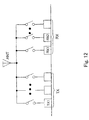
- FIG. 12 is a schematic diagram showing a configuration example of a mobile communication device including the high-frequency semiconductor switching circuit according to Embodiment 3 of the present invention.
- the mobile communication device shown in FIG. 12 is a device configured to switch the transmission and reception with respect to an antenna ANT and handle two or more types of electric power, such as high electric power and low electric power, which are different in magnitude.
- the mobile communication device shown in FIG. 12 uses a quasi-microwave hand as a communication band.
- the mobile communication device shown in FIG. 12 includes the high-frequency semiconductor switching circuit configured to perform switching of at least three high-frequency signals with respect to the antenna ANT. Specifically, one high-frequency signal is transmitted from a transmitting circuit TX 1 , and two high-frequency signals are respectively received by receiving circuits RX 1 and RX 2 .
- the MOSFET constituting the high-frequency signal path handles high electric power
- strain tends to occur in the MOSFET of the cutoff state. Therefore, by connecting a plurality of MOSFETs in series, the high-frequency signal of high electric power can be handled.
- the present embodiment in a case where the type of electric power to be handled is different among a plurality of high-frequency signal paths, and there are a plurality of high-frequency signal paths on the reception side, a part of the MOSFETs of the path switching FET stages provided on the plurality of high-frequency signal paths on the reception side are integrated. With this, an antenna switching circuit having the same level of strain property as a conventional antenna switching circuit can be further reduced in size.
- FIG. 13 is a circuit diagram showing a configuration example of the high-frequency semiconductor switching circuit according to Embodiment 3 of the present invention.
- the common input-output terminal 101 is used as the antenna ANT of FIG. 12
- the individual input-output terminal 102 is used as a terminal of the transmitting circuit TX 1 side of FIG. 12
- the individual input-output terminal 103 is used as a terminal of the receiving circuit RX 1 side of FIG. 12
- the individual input-output terminal 104 is used as a terminal of the receiving circuit RX 2 side of FIG. 12 .
- the high-frequency semiconductor switching circuit of FIG. 13 includes the common input-output terminal 101 , the individual input-output terminals 102 to 104 , the control terminals 105 to 107 , the PN junction diodes 126 to 131 , the PMOSFETs 332 to 337 , and the ground resistors 138 to 140 . These components are the same as those of the high-frequency semiconductor switching circuit of FIG. 5 .
- the path switching FET stage 108 is configured by connecting, for example, four path switching FETs 108 a to 108 d in series, gate resistors 114 a to 114 d are respectively connected to gates of the path switching FETs 108 a to 108 d , and short circuit resistors 120 a to 120 d are respectively connected between sources and drains of the path switching FETs 108 a to 108 d .
- the shunt FET stage 111 is configured by connecting, for example, four shunt FETs 111 a to 111 d in series, gate resistors 117 a to 117 d are respectively connected to gates of the shunt FETs 111 a to 111 d , and short circuit resistors 123 a to 123 d are respectively connected between sources and drains of the shunt FETs 111 a to 111 d.
- the path switching FET stage 109 is configured by connecting, for example, two MOSFETs 109 a and 109 b in series
- the path switching FET stage 110 is configured by connecting, for example, two MOSFETs 110 a and 110 b in series.
- the drain sides of the path switching FET stages 109 and 110 are short-circuited, and its short-circuit point is connected through a common path switching FET stage 1044 to the common input-output terminal 101 .
- Gates of the MOSFETs 109 a and 109 b are respectively connected to gate resistors 115 a and 115 b , a short circuit resistor 121 a is connected between a source and drain of the MOSFET 109 a , and a short circuit resistor 121 b is connected between a source and drain of the MOSFET 109 b .
- Gates of the MOSFETs 110 a and 110 b are respectively connected to gate resistors 116 a and 116 b , a short circuit resistor 122 a is connected between a source and drain of the MOSFET 110 a , and a short circuit resistor 122 b is connected between a source and drain of the MOSFET 110 b.
- the shunt FET stage 112 is configured by connecting, for example, two shunt FETs 112 a and 112 b in series
- the shunt FET stage 113 is configured by connecting, for example, two shunt FETs 113 a and 113 b .
- the drains of the shunt FET stages 112 and 113 are respectively connected to the individual input-output terminals 103 and 104 .
- Gates of the shunt FETs 112 a and 112 b are respectively connected to the gate resistors 118 a and 118 b , and a short circuit resistor 124 a is connected between a source and drain of the shunt FET stage 112 a , and a short circuit resistor 124 b is connected between a source and drain of the shunt FET stage 112 b .
- Gates of the shunt FETs 113 a and 113 b are respectively connected to gate resistors 119 a and 119 b , and a short circuit resistor 125 a is connected between a source and drain of the shunt FET stage 113 a , and a short circuit resistor 125 b is connected between a source and drain of the shunt FET stage 113 b.
- Gates of two common path switching FETs 1044 a and 1044 b constituting the common path switching FET stage 1044 are respectively connected to gate resistors 1045 a and 1045 b , a gate resistor 1046 a is connected between a source and drain of the common path switching FET 1044 a , and a gate resistor 1046 b is connected between a source and drain of the common path switching FET 1044 b .
- An anode side of a diode 1041 is connected to the control terminal 107
- an anode side of a diode 1042 is connected to the control terminal 106 .
- Cathode sides of the diodes 1041 and 1042 are short-circuited, and its short-circuit point is connected through the gate resistors 1045 a and 1045 b to the gates of the common path switching FETs 1044 a and 1044 b and connected through a ground resistor 1043 to the ground.
- the diode-switch logic circuit 100 performs the same operations as the circuit of FIG. 5 , the path switching FET stages 108 to 110 and the shunt FET stages 111 to 113 operate in accordance with the truth table of FIG. 2 .
- a voltage which has dropped from a voltage, determined by the logical sum of a voltage applied to the control terminal 106 and a voltage applied to the control terminal 107 , by the forward voltage of one diode is applied to each of the gates of the common path switching FETs 1044 a and 1044 b constituting the common path switching FET stage 1044 . Therefore, only when the path switching FET stage 109 or the path switching FET stage 110 is the conducting state, the common path switching FET stage 1044 becomes the conducting state.
- two or more high-frequency signal paths such as the paths of the receiving circuit RX 1 and the receiving circuit RX 2 or the paths of the receiving circuit RX 1 and the transmitting circuit TX 1 , may become the conducting state.
- a part of MOSFETs constituting two or more reception-side path switching FET stages configured to handle the high-frequency signal of low electric power can be integrated, and the integrated MOSFET can be controlled by the diode-switch logic circuit 100 .
- a high-function high-frequency switching circuit capable of causing two or more path switching FET stages to become the conducting state at the same time can be realized while maintaining satisfactory properties, such as the low insertion loss, the high isolation, and the low strain, and realizing the size reduction and the low power consumption without adding a power supply terminal.
- Embodiment 1 Basically, the same modification example as Embodiment 1 is applicable to the present embodiment.
- the diode-switch logic circuit 100 may be configured as a separate circuit as long as the separate circuit can perform the same operations as the configuration of FIG. 13 .
- the PMOSFETs 332 to 337 may be inversion control switches, and the diodes 126 to 131 , 1041 , and 1042 may be diode-connected NMOSFETs.
- the SP3T switch including one input and three outputs has been explained as one example of the high-frequency semiconductor switching circuit.
- the present embodiment is applicable to a wide range of multi-input multi-output high-frequency semiconductor switching circuits, such as the SP4T switch.
- the shunt FETs for securing the isolation are respectively connected to the high-frequency signal paths.
- the present embodiment is applicable to a case where one shunt FET is only connected to one specific high-frequency signal path.
- each of the path switching FET stage and the shunt FET stage is constituted by four FETs
- the common path switching FET stage is constituted by two FETs
- each of the path switching FET stages and the shunt FET stages is constituted by two FETs.
- the present embodiment is not limited to this.
- the SP3T switch a part of two high-frequency signal paths at the receiving portion RX side are formed as the common path switching FET stage 1044 .
- the number of high-frequency signal paths to be integrated is not limited to this.
- MOSFETs formed as a part of three or more high-frequency signal paths may be integrated.
- the number of short circuit resistors connected between the source and drain of each FET may be one or may be zero.
- the high-frequency semiconductor switching circuit of the present invention is useful for mobile communication devices, such as mobile phones, which are required to be small in size, light in weight, and low in power consumption.
Landscapes
- Physics & Mathematics (AREA)
- Engineering & Computer Science (AREA)
- Computer Hardware Design (AREA)
- Computing Systems (AREA)
- General Engineering & Computer Science (AREA)
- Mathematical Physics (AREA)
- Electronic Switches (AREA)
Applications Claiming Priority (3)
| Application Number | Priority Date | Filing Date | Title |
|---|---|---|---|
| JP2010-262705 | 2010-11-25 | ||
| JP2010262705A JP5366914B2 (ja) | 2010-11-25 | 2010-11-25 | 高周波半導体スイッチ回路 |
| PCT/JP2011/001245 WO2012070162A1 (ja) | 2010-11-25 | 2011-03-03 | 高周波半導体スイッチ回路 |
Related Parent Applications (1)
| Application Number | Title | Priority Date | Filing Date |
|---|---|---|---|
| PCT/JP2011/001245 Continuation WO2012070162A1 (ja) | 2010-11-25 | 2011-03-03 | 高周波半導体スイッチ回路 |
Publications (2)
| Publication Number | Publication Date |
|---|---|
| US20130127495A1 US20130127495A1 (en) | 2013-05-23 |
| US8884650B2 true US8884650B2 (en) | 2014-11-11 |
Family
ID=46145536
Family Applications (1)
| Application Number | Title | Priority Date | Filing Date |
|---|---|---|---|
| US13/741,999 Active 2031-05-15 US8884650B2 (en) | 2010-11-25 | 2013-01-15 | High-frequency semiconductor switching circuit |
Country Status (3)
| Country | Link |
|---|---|
| US (1) | US8884650B2 (ja) |
| JP (1) | JP5366914B2 (ja) |
| WO (1) | WO2012070162A1 (ja) |
Cited By (1)
| Publication number | Priority date | Publication date | Assignee | Title |
|---|---|---|---|---|
| US10629972B2 (en) | 2017-11-08 | 2020-04-21 | Pegatron Corporation | Radio-frequency switching circuit |
Families Citing this family (10)
| Publication number | Priority date | Publication date | Assignee | Title |
|---|---|---|---|---|
| US9231578B2 (en) | 2012-01-06 | 2016-01-05 | Richwave Technology Corp. | Apparatus and method for obtaining auxiliary voltage from control signals |
| US9543929B2 (en) | 2012-01-06 | 2017-01-10 | Richwave Technology Corp. | Apparatus and method for obtaining power voltage from control signals |
| JP6120227B2 (ja) | 2012-08-09 | 2017-04-26 | パナソニックIpマネジメント株式会社 | 高周波半導体スイッチ回路とそれを備えた高周波無線システム |
| JP2015226262A (ja) * | 2014-05-29 | 2015-12-14 | 株式会社東芝 | 半導体スイッチ、無線機器、及び、半導体スイッチの設計方法 |
| JP7007875B2 (ja) | 2017-11-24 | 2022-01-25 | 国立大学法人豊橋技術科学大学 | 高周波発振装置およびこれを用いた無線給電装置 |
| WO2019172903A1 (en) * | 2018-03-07 | 2019-09-12 | Intel IP Corporation | Interface circuitry with series switch and shunt attenuator |
| TWI676366B (zh) | 2018-08-10 | 2019-11-01 | 立積電子股份有限公司 | 射頻裝置及其電壓產生電路 |
| TWI734221B (zh) | 2019-10-16 | 2021-07-21 | 立積電子股份有限公司 | 射頻裝置及其電壓產生裝置 |
| CN115085759A (zh) | 2019-10-17 | 2022-09-20 | 立积电子股份有限公司 | 射频装置 |
| TWI819264B (zh) | 2020-12-25 | 2023-10-21 | 立積電子股份有限公司 | 射頻裝置及其電壓產生與諧波抑制器 |
Citations (9)
| Publication number | Priority date | Publication date | Assignee | Title |
|---|---|---|---|---|
| JPH0685641A (ja) | 1992-08-31 | 1994-03-25 | Mitsubishi Electric Corp | マイクロ波スイッチ |
| JPH08250648A (ja) | 1995-03-08 | 1996-09-27 | Rohm Co Ltd | 半導体装置およびそれを用いた論理回路 |
| JP2001068984A (ja) | 1999-08-25 | 2001-03-16 | Nec Corp | 半導体スイッチ回路及び移動体通信端末装置 |
| US20050017789A1 (en) * | 2001-10-10 | 2005-01-27 | Burgener Mark L. | Switch circuit and method of switching radio frequency signals |
| US20060001473A1 (en) * | 2004-06-30 | 2006-01-05 | Matsushita Electric Industrial Co., Ltd. | High frequency switching circuit device |
| JP2006050583A (ja) | 2004-06-30 | 2006-02-16 | Matsushita Electric Ind Co Ltd | 高周波スイッチ回路装置 |
| US7173471B2 (en) * | 2003-06-13 | 2007-02-06 | Matsushita Electric Industrial Co., Ltd. | High frequency switching circuit and semiconductor device |
| US7589602B2 (en) * | 2005-07-22 | 2009-09-15 | Stmicroelectronics S.A. | Antenna switch module |
| US7636004B2 (en) * | 2003-06-12 | 2009-12-22 | Panasonic Corporation | High-frequency switching device and semiconductor |
Family Cites Families (1)
| Publication number | Priority date | Publication date | Assignee | Title |
|---|---|---|---|---|
| JP4945215B2 (ja) * | 2006-10-27 | 2012-06-06 | 新日本無線株式会社 | 半導体スイッチ集積回路 |
-
2010
- 2010-11-25 JP JP2010262705A patent/JP5366914B2/ja not_active Expired - Fee Related
-
2011
- 2011-03-03 WO PCT/JP2011/001245 patent/WO2012070162A1/ja active Application Filing
-
2013
- 2013-01-15 US US13/741,999 patent/US8884650B2/en active Active
Patent Citations (11)
| Publication number | Priority date | Publication date | Assignee | Title |
|---|---|---|---|---|
| JPH0685641A (ja) | 1992-08-31 | 1994-03-25 | Mitsubishi Electric Corp | マイクロ波スイッチ |
| JPH08250648A (ja) | 1995-03-08 | 1996-09-27 | Rohm Co Ltd | 半導体装置およびそれを用いた論理回路 |
| JP2001068984A (ja) | 1999-08-25 | 2001-03-16 | Nec Corp | 半導体スイッチ回路及び移動体通信端末装置 |
| US20050017789A1 (en) * | 2001-10-10 | 2005-01-27 | Burgener Mark L. | Switch circuit and method of switching radio frequency signals |
| US7636004B2 (en) * | 2003-06-12 | 2009-12-22 | Panasonic Corporation | High-frequency switching device and semiconductor |
| US7173471B2 (en) * | 2003-06-13 | 2007-02-06 | Matsushita Electric Industrial Co., Ltd. | High frequency switching circuit and semiconductor device |
| US20060001473A1 (en) * | 2004-06-30 | 2006-01-05 | Matsushita Electric Industrial Co., Ltd. | High frequency switching circuit device |
| JP2006050583A (ja) | 2004-06-30 | 2006-02-16 | Matsushita Electric Ind Co Ltd | 高周波スイッチ回路装置 |
| US7337547B2 (en) * | 2004-06-30 | 2008-03-04 | Matsushita Electric Industrial Co., Ltd. | High frequency switching circuit device |
| JP4105183B2 (ja) | 2004-06-30 | 2008-06-25 | 松下電器産業株式会社 | 高周波スイッチ回路装置 |
| US7589602B2 (en) * | 2005-07-22 | 2009-09-15 | Stmicroelectronics S.A. | Antenna switch module |
Non-Patent Citations (1)
| Title |
|---|
| International Search Report issued in International Patent Application No. PCT/JP2011/001245 mailed Apr. 19, 2011. |
Cited By (1)
| Publication number | Priority date | Publication date | Assignee | Title |
|---|---|---|---|---|
| US10629972B2 (en) | 2017-11-08 | 2020-04-21 | Pegatron Corporation | Radio-frequency switching circuit |
Also Published As
| Publication number | Publication date |
|---|---|
| WO2012070162A1 (ja) | 2012-05-31 |
| JP5366914B2 (ja) | 2013-12-11 |
| JP2012114729A (ja) | 2012-06-14 |
| US20130127495A1 (en) | 2013-05-23 |
Similar Documents
| Publication | Publication Date | Title |
|---|---|---|
| US8884650B2 (en) | High-frequency semiconductor switching circuit | |
| US7337547B2 (en) | High frequency switching circuit device | |
| US8476961B2 (en) | System and method of transistor switch biasing in a high power semiconductor switch | |
| KR100244845B1 (ko) | 무선 주파 스위치 | |
| KR101218993B1 (ko) | 고주파 스위치 | |
| US20070290744A1 (en) | Radio frequency switching circuit, radio frequency switching device, and transmitter module device | |
| EP2775622A1 (en) | RF switch gate control | |
| US9048840B2 (en) | 20V to 250V high current ASIC PIN diode driver | |
| US6967517B2 (en) | Switching device | |
| US20100207679A1 (en) | Conduction switching circuit, conduction switching circuit block, and operating method of conduction switching circuit | |
| US11196453B2 (en) | High-power hybrid SPDT switch | |
| US9312853B2 (en) | High frequency semiconductor switch circuit and high frequency radio system including same | |
| US20140125402A1 (en) | Switching circuit, radio switching circuit, and switching method thereof | |
| US11777498B2 (en) | High power RF switch with controlled well voltage for improved linearity | |
| KR20110089636A (ko) | Rf 스위치 회로 | |
| US20130257510A1 (en) | High frequency switch circuit | |
| KR20070006851A (ko) | 낮은 대기 전류를 제공하는 고주파 스위치 디코더 | |
| JP4105183B2 (ja) | 高周波スイッチ回路装置 | |
| US9692410B2 (en) | Semiconductor switch | |
| US10491113B1 (en) | Transmit-receive system having three operating modes | |
| US11088685B2 (en) | High-frequency switch | |
| US11742848B1 (en) | High-voltage transmission gate architecture | |
| US20050190691A1 (en) | High-frequency switch apparatus | |
| JP2007006179A (ja) | アンテナスイッチ回路装置 | |
| WO2024073556A1 (en) | Methods and devices to control radiated spurious emission in rf antenna switches |
Legal Events
| Date | Code | Title | Description |
|---|---|---|---|
| AS | Assignment |
Owner name: PANASONIC CORPORATION, JAPAN Free format text: ASSIGNMENT OF ASSIGNORS INTEREST;ASSIGNOR:MIYAZAKI, TAKAHITO;REEL/FRAME:032005/0696 Effective date: 20121226 |
|
| STCF | Information on status: patent grant |
Free format text: PATENTED CASE |
|
| MAFP | Maintenance fee payment |
Free format text: PAYMENT OF MAINTENANCE FEE, 4TH YEAR, LARGE ENTITY (ORIGINAL EVENT CODE: M1551) Year of fee payment: 4 |
|
| AS | Assignment |
Owner name: PANASONIC SEMICONDUCTOR SOLUTIONS CO., LTD., JAPAN Free format text: ASSIGNMENT OF ASSIGNORS INTEREST;ASSIGNOR:PANASONIC CORPORATION;REEL/FRAME:052755/0917 Effective date: 20200521 |
|
| MAFP | Maintenance fee payment |
Free format text: PAYMENT OF MAINTENANCE FEE, 8TH YEAR, LARGE ENTITY (ORIGINAL EVENT CODE: M1552); ENTITY STATUS OF PATENT OWNER: LARGE ENTITY Year of fee payment: 8 |