US8872211B2 - Element-connecting board, producing method thereof, and light-emitting diode device - Google Patents
Element-connecting board, producing method thereof, and light-emitting diode device Download PDFInfo
- Publication number
- US8872211B2 US8872211B2 US13/690,494 US201213690494A US8872211B2 US 8872211 B2 US8872211 B2 US 8872211B2 US 201213690494 A US201213690494 A US 201213690494A US 8872211 B2 US8872211 B2 US 8872211B2
- Authority
- US
- United States
- Prior art keywords
- lead
- linear portions
- group
- insulating resin
- emitting diode
- Prior art date
- Legal status (The legal status is an assumption and is not a legal conclusion. Google has not performed a legal analysis and makes no representation as to the accuracy of the status listed.)
- Expired - Fee Related
Links
- 238000000034 method Methods 0.000 title description 22
- 229920005989 resin Polymers 0.000 claims abstract description 90
- 239000011347 resin Substances 0.000 claims abstract description 90
- 239000011342 resin composition Substances 0.000 claims description 58
- 238000004519 manufacturing process Methods 0.000 claims description 12
- 238000005520 cutting process Methods 0.000 claims description 9
- 125000001183 hydrocarbyl group Chemical group 0.000 description 42
- -1 polysiloxane Polymers 0.000 description 38
- 239000003054 catalyst Substances 0.000 description 37
- 150000003377 silicon compounds Chemical class 0.000 description 36
- 229920001296 polysiloxane Polymers 0.000 description 29
- 125000005372 silanol group Chemical group 0.000 description 29
- 239000000463 material Substances 0.000 description 27
- 230000005494 condensation Effects 0.000 description 25
- 238000009833 condensation Methods 0.000 description 24
- 125000003700 epoxy group Chemical group 0.000 description 24
- GWEVSGVZZGPLCZ-UHFFFAOYSA-N Titan oxide Chemical compound O=[Ti]=O GWEVSGVZZGPLCZ-UHFFFAOYSA-N 0.000 description 18
- 229920002050 silicone resin Polymers 0.000 description 18
- 239000011256 inorganic filler Substances 0.000 description 17
- 229910003475 inorganic filler Inorganic materials 0.000 description 17
- 238000002156 mixing Methods 0.000 description 16
- 229930195735 unsaturated hydrocarbon Natural products 0.000 description 16
- 238000006482 condensation reaction Methods 0.000 description 15
- 125000004432 carbon atom Chemical group C* 0.000 description 14
- 125000004435 hydrogen atom Chemical group [H]* 0.000 description 12
- 125000002029 aromatic hydrocarbon group Chemical group 0.000 description 10
- 239000000203 mixture Substances 0.000 description 10
- BASFCYQUMIYNBI-UHFFFAOYSA-N platinum Chemical compound [Pt] BASFCYQUMIYNBI-UHFFFAOYSA-N 0.000 description 10
- 229930195734 saturated hydrocarbon Natural products 0.000 description 10
- VYPSYNLAJGMNEJ-UHFFFAOYSA-N Silicium dioxide Chemical compound O=[Si]=O VYPSYNLAJGMNEJ-UHFFFAOYSA-N 0.000 description 9
- 125000003545 alkoxy group Chemical group 0.000 description 9
- 239000003822 epoxy resin Substances 0.000 description 8
- 125000002496 methyl group Chemical group [H]C([H])([H])* 0.000 description 8
- 238000001579 optical reflectometry Methods 0.000 description 8
- 239000002245 particle Substances 0.000 description 8
- 229920000647 polyepoxide Polymers 0.000 description 8
- OGIDPMRJRNCKJF-UHFFFAOYSA-N titanium oxide Inorganic materials [Ti]=O OGIDPMRJRNCKJF-UHFFFAOYSA-N 0.000 description 8
- 229910020175 SiOH Inorganic materials 0.000 description 6
- 238000007259 addition reaction Methods 0.000 description 6
- 239000013078 crystal Substances 0.000 description 6
- 125000000524 functional group Chemical group 0.000 description 6
- 229910052751 metal Inorganic materials 0.000 description 6
- 239000002184 metal Substances 0.000 description 6
- 229910052697 platinum Inorganic materials 0.000 description 6
- SCPYDCQAZCOKTP-UHFFFAOYSA-N silanol Chemical compound [SiH3]O SCPYDCQAZCOKTP-UHFFFAOYSA-N 0.000 description 6
- 125000003342 alkenyl group Chemical group 0.000 description 5
- GYZLOYUZLJXAJU-UHFFFAOYSA-N diglycidyl ether Chemical group C1OC1COCC1CO1 GYZLOYUZLJXAJU-UHFFFAOYSA-N 0.000 description 5
- 125000005843 halogen group Chemical group 0.000 description 5
- 238000010438 heat treatment Methods 0.000 description 5
- 230000008569 process Effects 0.000 description 5
- VTYYLEPIZMXCLO-UHFFFAOYSA-L Calcium carbonate Chemical compound [Ca+2].[O-]C([O-])=O VTYYLEPIZMXCLO-UHFFFAOYSA-L 0.000 description 4
- 239000003795 chemical substances by application Substances 0.000 description 4
- 238000004040 coloring Methods 0.000 description 4
- 239000007788 liquid Substances 0.000 description 4
- 230000009257 reactivity Effects 0.000 description 4
- 239000000377 silicon dioxide Substances 0.000 description 4
- WGTYBPLFGIVFAS-UHFFFAOYSA-M tetramethylammonium hydroxide Chemical compound [OH-].C[N+](C)(C)C WGTYBPLFGIVFAS-UHFFFAOYSA-M 0.000 description 4
- 238000005160 1H NMR spectroscopy Methods 0.000 description 3
- QTBSBXVTEAMEQO-UHFFFAOYSA-N Acetic acid Chemical compound CC(O)=O QTBSBXVTEAMEQO-UHFFFAOYSA-N 0.000 description 3
- 239000004593 Epoxy Substances 0.000 description 3
- LFQSCWFLJHTTHZ-UHFFFAOYSA-N Ethanol Chemical compound CCO LFQSCWFLJHTTHZ-UHFFFAOYSA-N 0.000 description 3
- OKKJLVBELUTLKV-UHFFFAOYSA-N Methanol Chemical compound OC OKKJLVBELUTLKV-UHFFFAOYSA-N 0.000 description 3
- KWYUFKZDYYNOTN-UHFFFAOYSA-M Potassium hydroxide Chemical compound [OH-].[K+] KWYUFKZDYYNOTN-UHFFFAOYSA-M 0.000 description 3
- HEMHJVSKTPXQMS-UHFFFAOYSA-M Sodium hydroxide Chemical compound [OH-].[Na+] HEMHJVSKTPXQMS-UHFFFAOYSA-M 0.000 description 3
- YXFVVABEGXRONW-UHFFFAOYSA-N Toluene Chemical compound CC1=CC=CC=C1 YXFVVABEGXRONW-UHFFFAOYSA-N 0.000 description 3
- 125000000217 alkyl group Chemical group 0.000 description 3
- 238000006243 chemical reaction Methods 0.000 description 3
- RKTYLMNFRDHKIL-UHFFFAOYSA-N copper;5,10,15,20-tetraphenylporphyrin-22,24-diide Chemical compound [Cu+2].C1=CC(C(=C2C=CC([N-]2)=C(C=2C=CC=CC=2)C=2C=CC(N=2)=C(C=2C=CC=CC=2)C2=CC=C3[N-]2)C=2C=CC=CC=2)=NC1=C3C1=CC=CC=C1 RKTYLMNFRDHKIL-UHFFFAOYSA-N 0.000 description 3
- 125000000392 cycloalkenyl group Chemical group 0.000 description 3
- 239000004205 dimethyl polysiloxane Substances 0.000 description 3
- 230000000694 effects Effects 0.000 description 3
- 238000006459 hydrosilylation reaction Methods 0.000 description 3
- 239000001023 inorganic pigment Substances 0.000 description 3
- 239000010410 layer Substances 0.000 description 3
- 125000000956 methoxy group Chemical group [H]C([H])([H])O* 0.000 description 3
- 125000001997 phenyl group Chemical group [H]C1=C([H])C([H])=C(*)C([H])=C1[H] 0.000 description 3
- 229920000435 poly(dimethylsiloxane) Polymers 0.000 description 3
- 239000007787 solid Substances 0.000 description 3
- 239000002904 solvent Substances 0.000 description 3
- 238000003756 stirring Methods 0.000 description 3
- 239000000126 substance Substances 0.000 description 3
- VEXZGXHMUGYJMC-UHFFFAOYSA-N Hydrochloric acid Chemical compound Cl VEXZGXHMUGYJMC-UHFFFAOYSA-N 0.000 description 2
- UQSXHKLRYXJYBZ-UHFFFAOYSA-N Iron oxide Chemical compound [Fe]=O UQSXHKLRYXJYBZ-UHFFFAOYSA-N 0.000 description 2
- PXHVJJICTQNCMI-UHFFFAOYSA-N Nickel Chemical compound [Ni] PXHVJJICTQNCMI-UHFFFAOYSA-N 0.000 description 2
- KDLHZDBZIXYQEI-UHFFFAOYSA-N Palladium Chemical compound [Pd] KDLHZDBZIXYQEI-UHFFFAOYSA-N 0.000 description 2
- QAOWNCQODCNURD-UHFFFAOYSA-N Sulfuric acid Chemical compound OS(O)(=O)=O QAOWNCQODCNURD-UHFFFAOYSA-N 0.000 description 2
- XLOMVQKBTHCTTD-UHFFFAOYSA-N Zinc monoxide Chemical compound [Zn]=O XLOMVQKBTHCTTD-UHFFFAOYSA-N 0.000 description 2
- 125000003668 acetyloxy group Chemical group [H]C([H])([H])C(=O)O[*] 0.000 description 2
- 239000002253 acid Substances 0.000 description 2
- 150000008065 acid anhydrides Chemical class 0.000 description 2
- 239000012790 adhesive layer Substances 0.000 description 2
- 125000002947 alkylene group Chemical group 0.000 description 2
- 125000003118 aryl group Chemical group 0.000 description 2
- TZCXTZWJZNENPQ-UHFFFAOYSA-L barium sulfate Chemical compound [Ba+2].[O-]S([O-])(=O)=O TZCXTZWJZNENPQ-UHFFFAOYSA-L 0.000 description 2
- 229910000019 calcium carbonate Inorganic materials 0.000 description 2
- 150000001875 compounds Chemical class 0.000 description 2
- 239000004020 conductor Substances 0.000 description 2
- 125000000753 cycloalkyl group Chemical group 0.000 description 2
- 238000005530 etching Methods 0.000 description 2
- NKSJNEHGWDZZQF-UHFFFAOYSA-N ethenyl(trimethoxy)silane Chemical compound CO[Si](OC)(OC)C=C NKSJNEHGWDZZQF-UHFFFAOYSA-N 0.000 description 2
- NLYAJNPCOHFWQQ-UHFFFAOYSA-N kaolin Chemical compound O.O.O=[Al]O[Si](=O)O[Si](=O)O[Al]=O NLYAJNPCOHFWQQ-UHFFFAOYSA-N 0.000 description 2
- BDAGIHXWWSANSR-UHFFFAOYSA-N methanoic acid Natural products OC=O BDAGIHXWWSANSR-UHFFFAOYSA-N 0.000 description 2
- JRZJOMJEPLMPRA-UHFFFAOYSA-N olefin Natural products CCCCCCCC=C JRZJOMJEPLMPRA-UHFFFAOYSA-N 0.000 description 2
- 230000003287 optical effect Effects 0.000 description 2
- 229920006136 organohydrogenpolysiloxane Polymers 0.000 description 2
- 125000005375 organosiloxane group Chemical group 0.000 description 2
- 125000000951 phenoxy group Chemical group [H]C1=C([H])C([H])=C(O*)C([H])=C1[H] 0.000 description 2
- 229920001921 poly-methyl-phenyl-siloxane Polymers 0.000 description 2
- BWHMMNNQKKPAPP-UHFFFAOYSA-L potassium carbonate Chemical compound [K+].[K+].[O-]C([O-])=O BWHMMNNQKKPAPP-UHFFFAOYSA-L 0.000 description 2
- 125000004805 propylene group Chemical group [H]C([H])([H])C([H])([*:1])C([H])([H])[*:2] 0.000 description 2
- 238000004080 punching Methods 0.000 description 2
- 239000004065 semiconductor Substances 0.000 description 2
- 229910000077 silane Inorganic materials 0.000 description 2
- 150000004756 silanes Chemical class 0.000 description 2
- 235000012239 silicon dioxide Nutrition 0.000 description 2
- 238000009751 slip forming Methods 0.000 description 2
- 229920001187 thermosetting polymer Polymers 0.000 description 2
- BPSIOYPQMFLKFR-UHFFFAOYSA-N trimethoxy-[3-(oxiran-2-ylmethoxy)propyl]silane Chemical compound CO[Si](OC)(OC)CCCOCC1CO1 BPSIOYPQMFLKFR-UHFFFAOYSA-N 0.000 description 2
- 125000000391 vinyl group Chemical group [H]C([*])=C([H])[H] 0.000 description 2
- 239000012463 white pigment Substances 0.000 description 2
- MFEVGQHCNVXMER-UHFFFAOYSA-L 1,3,2$l^{2}-dioxaplumbetan-4-one Chemical compound [Pb+2].[O-]C([O-])=O MFEVGQHCNVXMER-UHFFFAOYSA-L 0.000 description 1
- 125000003903 2-propenyl group Chemical group [H]C([*])([H])C([H])=C([H])[H] 0.000 description 1
- JRGQKLFZSNYTDX-UHFFFAOYSA-N 3-(oxiran-2-ylmethoxy)propyl-tri(propan-2-yloxy)silane Chemical compound CC(C)O[Si](OC(C)C)(OC(C)C)CCCOCC1CO1 JRGQKLFZSNYTDX-UHFFFAOYSA-N 0.000 description 1
- DAJFVZRDKCROQC-UHFFFAOYSA-N 3-(oxiran-2-ylmethoxy)propyl-tripropoxysilane Chemical compound CCCO[Si](OCCC)(OCCC)CCCOCC1CO1 DAJFVZRDKCROQC-UHFFFAOYSA-N 0.000 description 1
- OSWFIVFLDKOXQC-UHFFFAOYSA-N 4-(3-methoxyphenyl)aniline Chemical compound COC1=CC=CC(C=2C=CC(N)=CC=2)=C1 OSWFIVFLDKOXQC-UHFFFAOYSA-N 0.000 description 1
- ZCYVEMRRCGMTRW-UHFFFAOYSA-N 7553-56-2 Chemical compound [I] ZCYVEMRRCGMTRW-UHFFFAOYSA-N 0.000 description 1
- 239000004925 Acrylic resin Substances 0.000 description 1
- 229920000178 Acrylic resin Polymers 0.000 description 1
- 239000005995 Aluminium silicate Substances 0.000 description 1
- WKBOTKDWSSQWDR-UHFFFAOYSA-N Bromine atom Chemical compound [Br] WKBOTKDWSSQWDR-UHFFFAOYSA-N 0.000 description 1
- BVKZGUZCCUSVTD-UHFFFAOYSA-L Carbonate Chemical compound [O-]C([O-])=O BVKZGUZCCUSVTD-UHFFFAOYSA-L 0.000 description 1
- KZBUYRJDOAKODT-UHFFFAOYSA-N Chlorine Chemical compound ClCl KZBUYRJDOAKODT-UHFFFAOYSA-N 0.000 description 1
- ZAMOUSCENKQFHK-UHFFFAOYSA-N Chlorine atom Chemical compound [Cl] ZAMOUSCENKQFHK-UHFFFAOYSA-N 0.000 description 1
- RYGMFSIKBFXOCR-UHFFFAOYSA-N Copper Chemical compound [Cu] RYGMFSIKBFXOCR-UHFFFAOYSA-N 0.000 description 1
- PXGOKWXKJXAPGV-UHFFFAOYSA-N Fluorine Chemical compound FF PXGOKWXKJXAPGV-UHFFFAOYSA-N 0.000 description 1
- 229910000003 Lead carbonate Inorganic materials 0.000 description 1
- 239000004793 Polystyrene Substances 0.000 description 1
- ATJFFYVFTNAWJD-UHFFFAOYSA-N Tin Chemical compound [Sn] ATJFFYVFTNAWJD-UHFFFAOYSA-N 0.000 description 1
- RTAQQCXQSZGOHL-UHFFFAOYSA-N Titanium Chemical compound [Ti] RTAQQCXQSZGOHL-UHFFFAOYSA-N 0.000 description 1
- 229910000004 White lead Inorganic materials 0.000 description 1
- HCHKCACWOHOZIP-UHFFFAOYSA-N Zinc Chemical compound [Zn] HCHKCACWOHOZIP-UHFFFAOYSA-N 0.000 description 1
- VBXBSTJDBPXOAD-UHFFFAOYSA-N acetyl acetate;platinum Chemical compound [Pt].CC(=O)OC(C)=O VBXBSTJDBPXOAD-UHFFFAOYSA-N 0.000 description 1
- 239000000956 alloy Substances 0.000 description 1
- 229910045601 alloy Inorganic materials 0.000 description 1
- 229910052782 aluminium Inorganic materials 0.000 description 1
- XAGFODPZIPBFFR-UHFFFAOYSA-N aluminium Chemical compound [Al] XAGFODPZIPBFFR-UHFFFAOYSA-N 0.000 description 1
- WNROFYMDJYEPJX-UHFFFAOYSA-K aluminium hydroxide Chemical compound [OH-].[OH-].[OH-].[Al+3] WNROFYMDJYEPJX-UHFFFAOYSA-K 0.000 description 1
- 235000012211 aluminium silicate Nutrition 0.000 description 1
- 150000004945 aromatic hydrocarbons Chemical class 0.000 description 1
- 125000000732 arylene group Chemical group 0.000 description 1
- JRPBQTZRNDNNOP-UHFFFAOYSA-N barium titanate Chemical compound [Ba+2].[Ba+2].[O-][Ti]([O-])([O-])[O-] JRPBQTZRNDNNOP-UHFFFAOYSA-N 0.000 description 1
- 229910002113 barium titanate Inorganic materials 0.000 description 1
- AYJRCSIUFZENHW-DEQYMQKBSA-L barium(2+);oxomethanediolate Chemical compound [Ba+2].[O-][14C]([O-])=O AYJRCSIUFZENHW-DEQYMQKBSA-L 0.000 description 1
- 230000008901 benefit Effects 0.000 description 1
- GDTBXPJZTBHREO-UHFFFAOYSA-N bromine Substances BrBr GDTBXPJZTBHREO-UHFFFAOYSA-N 0.000 description 1
- 229910052794 bromium Inorganic materials 0.000 description 1
- 125000004369 butenyl group Chemical group C(=CCC)* 0.000 description 1
- 125000004106 butoxy group Chemical group [*]OC([H])([H])C([H])([H])C(C([H])([H])[H])([H])[H] 0.000 description 1
- 125000000484 butyl group Chemical group [H]C([*])([H])C([H])([H])C([H])([H])C([H])([H])[H] 0.000 description 1
- 239000006229 carbon black Substances 0.000 description 1
- 239000000460 chlorine Substances 0.000 description 1
- 229910052801 chlorine Inorganic materials 0.000 description 1
- 239000002734 clay mineral Substances 0.000 description 1
- 230000006835 compression Effects 0.000 description 1
- 238000007906 compression Methods 0.000 description 1
- 239000000470 constituent Substances 0.000 description 1
- 229910052802 copper Inorganic materials 0.000 description 1
- 239000010949 copper Substances 0.000 description 1
- 125000002993 cycloalkylene group Chemical group 0.000 description 1
- MIZPLDZQVGUDMR-UHFFFAOYSA-N cyclohexen-1-yl(trimethoxy)silane Chemical compound CO[Si](OC)(OC)C1=CCCCC1 MIZPLDZQVGUDMR-UHFFFAOYSA-N 0.000 description 1
- 125000000596 cyclohexenyl group Chemical group C1(=CCCCC1)* 0.000 description 1
- 125000000113 cyclohexyl group Chemical group [H]C1([H])C([H])([H])C([H])([H])C([H])(*)C([H])([H])C1([H])[H] 0.000 description 1
- 125000004956 cyclohexylene group Chemical group 0.000 description 1
- 125000002933 cyclohexyloxy group Chemical group C1(CCCCC1)O* 0.000 description 1
- 125000001511 cyclopentyl group Chemical group [H]C1([H])C([H])([H])C([H])([H])C([H])(*)C1([H])[H] 0.000 description 1
- 125000004979 cyclopentylene group Chemical group 0.000 description 1
- 125000001887 cyclopentyloxy group Chemical group C1(CCCC1)O* 0.000 description 1
- 230000008034 disappearance Effects 0.000 description 1
- 239000006185 dispersion Substances 0.000 description 1
- 238000009826 distribution Methods 0.000 description 1
- FWDBOZPQNFPOLF-UHFFFAOYSA-N ethenyl(triethoxy)silane Chemical compound CCO[Si](OCC)(OCC)C=C FWDBOZPQNFPOLF-UHFFFAOYSA-N 0.000 description 1
- NNBRCHPBPDRPIT-UHFFFAOYSA-N ethenyl(tripropoxy)silane Chemical compound CCCO[Si](OCCC)(OCCC)C=C NNBRCHPBPDRPIT-UHFFFAOYSA-N 0.000 description 1
- RCNRJBWHLARWRP-UHFFFAOYSA-N ethenyl-[ethenyl(dimethyl)silyl]oxy-dimethylsilane;platinum Chemical compound [Pt].C=C[Si](C)(C)O[Si](C)(C)C=C RCNRJBWHLARWRP-UHFFFAOYSA-N 0.000 description 1
- 125000001301 ethoxy group Chemical group [H]C([H])([H])C([H])([H])O* 0.000 description 1
- 125000001495 ethyl group Chemical group [H]C([H])([H])C([H])([H])* 0.000 description 1
- 125000000816 ethylene group Chemical group [H]C([H])([*:1])C([H])([H])[*:2] 0.000 description 1
- 238000011049 filling Methods 0.000 description 1
- 229910052731 fluorine Inorganic materials 0.000 description 1
- 239000011737 fluorine Substances 0.000 description 1
- 235000019253 formic acid Nutrition 0.000 description 1
- 238000005227 gel permeation chromatography Methods 0.000 description 1
- 239000003365 glass fiber Substances 0.000 description 1
- 125000005417 glycidoxyalkyl group Chemical group 0.000 description 1
- PCHJSUWPFVWCPO-UHFFFAOYSA-N gold Chemical compound [Au] PCHJSUWPFVWCPO-UHFFFAOYSA-N 0.000 description 1
- 229910052737 gold Inorganic materials 0.000 description 1
- 239000010931 gold Substances 0.000 description 1
- 125000006038 hexenyl group Chemical group 0.000 description 1
- 125000004051 hexyl group Chemical group [H]C([H])([H])C([H])([H])C([H])([H])C([H])([H])C([H])([H])C([H])([H])* 0.000 description 1
- 125000003707 hexyloxy group Chemical group [H]C([H])([H])C([H])([H])C([H])([H])C([H])([H])C([H])([H])C([H])([H])O* 0.000 description 1
- 229910052740 iodine Inorganic materials 0.000 description 1
- 239000011630 iodine Substances 0.000 description 1
- 125000002510 isobutoxy group Chemical group [H]C([H])([H])C([H])(C([H])([H])[H])C([H])([H])O* 0.000 description 1
- 125000000959 isobutyl group Chemical group [H]C([H])([H])C([H])(C([H])([H])[H])C([H])([H])* 0.000 description 1
- 125000003253 isopropoxy group Chemical group [H]C([H])([H])C([H])(O*)C([H])([H])[H] 0.000 description 1
- 125000001449 isopropyl group Chemical group [H]C([H])([H])C([H])(*)C([H])([H])[H] 0.000 description 1
- 229910052622 kaolinite Inorganic materials 0.000 description 1
- 238000003475 lamination Methods 0.000 description 1
- 239000000395 magnesium oxide Substances 0.000 description 1
- CPLXHLVBOLITMK-UHFFFAOYSA-N magnesium oxide Inorganic materials [Mg]=O CPLXHLVBOLITMK-UHFFFAOYSA-N 0.000 description 1
- AXZKOIWUVFPNLO-UHFFFAOYSA-N magnesium;oxygen(2-) Chemical compound [O-2].[Mg+2] AXZKOIWUVFPNLO-UHFFFAOYSA-N 0.000 description 1
- 238000005259 measurement Methods 0.000 description 1
- 125000001570 methylene group Chemical group [H]C([H])([*:1])[*:2] 0.000 description 1
- 239000010445 mica Substances 0.000 description 1
- 229910052618 mica group Inorganic materials 0.000 description 1
- 230000004048 modification Effects 0.000 description 1
- 238000012986 modification Methods 0.000 description 1
- 125000001624 naphthyl group Chemical group 0.000 description 1
- 125000004957 naphthylene group Chemical group 0.000 description 1
- 229910052759 nickel Inorganic materials 0.000 description 1
- 125000003518 norbornenyl group Chemical group C12(C=CC(CC1)C2)* 0.000 description 1
- 125000004365 octenyl group Chemical group C(=CCCCCCC)* 0.000 description 1
- 239000003921 oil Substances 0.000 description 1
- RVTZCBVAJQQJTK-UHFFFAOYSA-N oxygen(2-);zirconium(4+) Chemical compound [O-2].[O-2].[Zr+4] RVTZCBVAJQQJTK-UHFFFAOYSA-N 0.000 description 1
- 229910052763 palladium Inorganic materials 0.000 description 1
- 125000002255 pentenyl group Chemical group C(=CCCC)* 0.000 description 1
- 125000004115 pentoxy group Chemical group [*]OC([H])([H])C([H])([H])C([H])([H])C(C([H])([H])[H])([H])[H] 0.000 description 1
- 125000001147 pentyl group Chemical group C(CCCC)* 0.000 description 1
- 125000000843 phenylene group Chemical group C1(=C(C=CC=C1)*)* 0.000 description 1
- CLSUSRZJUQMOHH-UHFFFAOYSA-L platinum dichloride Chemical compound Cl[Pt]Cl CLSUSRZJUQMOHH-UHFFFAOYSA-L 0.000 description 1
- 229920001721 polyimide Polymers 0.000 description 1
- 239000009719 polyimide resin Substances 0.000 description 1
- 229920002223 polystyrene Polymers 0.000 description 1
- 229910000027 potassium carbonate Inorganic materials 0.000 description 1
- 238000002360 preparation method Methods 0.000 description 1
- 125000004368 propenyl group Chemical group C(=CC)* 0.000 description 1
- 125000002572 propoxy group Chemical group [*]OC([H])([H])C(C([H])([H])[H])([H])[H] 0.000 description 1
- 125000001436 propyl group Chemical group [H]C([*])([H])C([H])([H])C([H])([H])[H] 0.000 description 1
- 230000009467 reduction Effects 0.000 description 1
- 238000002310 reflectometry Methods 0.000 description 1
- 229910052703 rhodium Inorganic materials 0.000 description 1
- 239000010948 rhodium Substances 0.000 description 1
- MHOVAHRLVXNVSD-UHFFFAOYSA-N rhodium atom Chemical compound [Rh] MHOVAHRLVXNVSD-UHFFFAOYSA-N 0.000 description 1
- 125000000383 tetramethylene group Chemical group [H]C([H])([*:1])C([H])([H])C([H])([H])C([H])([H])[*:2] 0.000 description 1
- 238000005979 thermal decomposition reaction Methods 0.000 description 1
- 229910052718 tin Inorganic materials 0.000 description 1
- 239000011135 tin Substances 0.000 description 1
- 239000010936 titanium Substances 0.000 description 1
- 229910052719 titanium Inorganic materials 0.000 description 1
- 239000004408 titanium dioxide Substances 0.000 description 1
- JXUKBNICSRJFAP-UHFFFAOYSA-N triethoxy-[3-(oxiran-2-ylmethoxy)propyl]silane Chemical compound CCO[Si](OCC)(OCC)CCCOCC1CO1 JXUKBNICSRJFAP-UHFFFAOYSA-N 0.000 description 1
- LFBULLRGNLZJAF-UHFFFAOYSA-N trimethoxy(oxiran-2-ylmethoxymethyl)silane Chemical compound CO[Si](OC)(OC)COCC1CO1 LFBULLRGNLZJAF-UHFFFAOYSA-N 0.000 description 1
- OWUTVCVPEOXXHD-UHFFFAOYSA-N trimethoxy(prop-1-enyl)silane Chemical compound CO[Si](OC)(OC)C=CC OWUTVCVPEOXXHD-UHFFFAOYSA-N 0.000 description 1
- LFRDHGNFBLIJIY-UHFFFAOYSA-N trimethoxy(prop-2-enyl)silane Chemical compound CO[Si](OC)(OC)CC=C LFRDHGNFBLIJIY-UHFFFAOYSA-N 0.000 description 1
- ZNXDCSVNCSSUNB-UHFFFAOYSA-N trimethoxy-[2-(oxiran-2-ylmethoxy)ethyl]silane Chemical compound CO[Si](OC)(OC)CCOCC1CO1 ZNXDCSVNCSSUNB-UHFFFAOYSA-N 0.000 description 1
- XLYOFNOQVPJJNP-UHFFFAOYSA-N water Substances O XLYOFNOQVPJJNP-UHFFFAOYSA-N 0.000 description 1
- 239000011701 zinc Substances 0.000 description 1
- 229910052725 zinc Inorganic materials 0.000 description 1
- 239000011787 zinc oxide Substances 0.000 description 1
- 229910001928 zirconium oxide Inorganic materials 0.000 description 1
Images


Classifications
-
- H—ELECTRICITY
- H01—ELECTRIC ELEMENTS
- H01L—SEMICONDUCTOR DEVICES NOT COVERED BY CLASS H10
- H01L33/00—Semiconductor devices having potential barriers specially adapted for light emission; Processes or apparatus specially adapted for the manufacture or treatment thereof or of parts thereof; Details thereof
- H01L33/48—Semiconductor devices having potential barriers specially adapted for light emission; Processes or apparatus specially adapted for the manufacture or treatment thereof or of parts thereof; Details thereof characterised by the semiconductor body packages
- H01L33/52—Encapsulations
-
- H—ELECTRICITY
- H01—ELECTRIC ELEMENTS
- H01L—SEMICONDUCTOR DEVICES NOT COVERED BY CLASS H10
- H01L33/00—Semiconductor devices having potential barriers specially adapted for light emission; Processes or apparatus specially adapted for the manufacture or treatment thereof or of parts thereof; Details thereof
- H01L33/48—Semiconductor devices having potential barriers specially adapted for light emission; Processes or apparatus specially adapted for the manufacture or treatment thereof or of parts thereof; Details thereof characterised by the semiconductor body packages
-
- H—ELECTRICITY
- H01—ELECTRIC ELEMENTS
- H01L—SEMICONDUCTOR DEVICES NOT COVERED BY CLASS H10
- H01L33/00—Semiconductor devices having potential barriers specially adapted for light emission; Processes or apparatus specially adapted for the manufacture or treatment thereof or of parts thereof; Details thereof
- H01L33/44—Semiconductor devices having potential barriers specially adapted for light emission; Processes or apparatus specially adapted for the manufacture or treatment thereof or of parts thereof; Details thereof characterised by the coatings, e.g. passivation layer or anti-reflective coating
- H01L33/46—Reflective coating, e.g. dielectric Bragg reflector
-
- F—MECHANICAL ENGINEERING; LIGHTING; HEATING; WEAPONS; BLASTING
- F21—LIGHTING
- F21V—FUNCTIONAL FEATURES OR DETAILS OF LIGHTING DEVICES OR SYSTEMS THEREOF; STRUCTURAL COMBINATIONS OF LIGHTING DEVICES WITH OTHER ARTICLES, NOT OTHERWISE PROVIDED FOR
- F21V21/00—Supporting, suspending, or attaching arrangements for lighting devices; Hand grips
-
- H—ELECTRICITY
- H01—ELECTRIC ELEMENTS
- H01L—SEMICONDUCTOR DEVICES NOT COVERED BY CLASS H10
- H01L33/00—Semiconductor devices having potential barriers specially adapted for light emission; Processes or apparatus specially adapted for the manufacture or treatment thereof or of parts thereof; Details thereof
- H01L33/48—Semiconductor devices having potential barriers specially adapted for light emission; Processes or apparatus specially adapted for the manufacture or treatment thereof or of parts thereof; Details thereof characterised by the semiconductor body packages
- H01L33/62—Arrangements for conducting electric current to or from the semiconductor body, e.g. lead-frames, wire-bonds or solder balls
-
- H—ELECTRICITY
- H05—ELECTRIC TECHNIQUES NOT OTHERWISE PROVIDED FOR
- H05K—PRINTED CIRCUITS; CASINGS OR CONSTRUCTIONAL DETAILS OF ELECTRIC APPARATUS; MANUFACTURE OF ASSEMBLAGES OF ELECTRICAL COMPONENTS
- H05K13/00—Apparatus or processes specially adapted for manufacturing or adjusting assemblages of electric components
-
- H—ELECTRICITY
- H01—ELECTRIC ELEMENTS
- H01L—SEMICONDUCTOR DEVICES NOT COVERED BY CLASS H10
- H01L2224/00—Indexing scheme for arrangements for connecting or disconnecting semiconductor or solid-state bodies and methods related thereto as covered by H01L24/00
- H01L2224/01—Means for bonding being attached to, or being formed on, the surface to be connected, e.g. chip-to-package, die-attach, "first-level" interconnects; Manufacturing methods related thereto
- H01L2224/42—Wire connectors; Manufacturing methods related thereto
- H01L2224/47—Structure, shape, material or disposition of the wire connectors after the connecting process
- H01L2224/48—Structure, shape, material or disposition of the wire connectors after the connecting process of an individual wire connector
- H01L2224/4805—Shape
- H01L2224/4809—Loop shape
- H01L2224/48091—Arched
-
- H—ELECTRICITY
- H01—ELECTRIC ELEMENTS
- H01L—SEMICONDUCTOR DEVICES NOT COVERED BY CLASS H10
- H01L2224/00—Indexing scheme for arrangements for connecting or disconnecting semiconductor or solid-state bodies and methods related thereto as covered by H01L24/00
- H01L2224/01—Means for bonding being attached to, or being formed on, the surface to be connected, e.g. chip-to-package, die-attach, "first-level" interconnects; Manufacturing methods related thereto
- H01L2224/42—Wire connectors; Manufacturing methods related thereto
- H01L2224/47—Structure, shape, material or disposition of the wire connectors after the connecting process
- H01L2224/48—Structure, shape, material or disposition of the wire connectors after the connecting process of an individual wire connector
- H01L2224/481—Disposition
- H01L2224/48151—Connecting between a semiconductor or solid-state body and an item not being a semiconductor or solid-state body, e.g. chip-to-substrate, chip-to-passive
- H01L2224/48221—Connecting between a semiconductor or solid-state body and an item not being a semiconductor or solid-state body, e.g. chip-to-substrate, chip-to-passive the body and the item being stacked
- H01L2224/48245—Connecting between a semiconductor or solid-state body and an item not being a semiconductor or solid-state body, e.g. chip-to-substrate, chip-to-passive the body and the item being stacked the item being metallic
- H01L2224/48247—Connecting between a semiconductor or solid-state body and an item not being a semiconductor or solid-state body, e.g. chip-to-substrate, chip-to-passive the body and the item being stacked the item being metallic connecting the wire to a bond pad of the item
-
- H—ELECTRICITY
- H01—ELECTRIC ELEMENTS
- H01L—SEMICONDUCTOR DEVICES NOT COVERED BY CLASS H10
- H01L25/00—Assemblies consisting of a plurality of individual semiconductor or other solid state devices ; Multistep manufacturing processes thereof
- H01L25/03—Assemblies consisting of a plurality of individual semiconductor or other solid state devices ; Multistep manufacturing processes thereof all the devices being of a type provided for in the same subgroup of groups H01L27/00 - H01L33/00, or in a single subclass of H10K, H10N, e.g. assemblies of rectifier diodes
- H01L25/04—Assemblies consisting of a plurality of individual semiconductor or other solid state devices ; Multistep manufacturing processes thereof all the devices being of a type provided for in the same subgroup of groups H01L27/00 - H01L33/00, or in a single subclass of H10K, H10N, e.g. assemblies of rectifier diodes the devices not having separate containers
- H01L25/075—Assemblies consisting of a plurality of individual semiconductor or other solid state devices ; Multistep manufacturing processes thereof all the devices being of a type provided for in the same subgroup of groups H01L27/00 - H01L33/00, or in a single subclass of H10K, H10N, e.g. assemblies of rectifier diodes the devices not having separate containers the devices being of a type provided for in group H01L33/00
- H01L25/0753—Assemblies consisting of a plurality of individual semiconductor or other solid state devices ; Multistep manufacturing processes thereof all the devices being of a type provided for in the same subgroup of groups H01L27/00 - H01L33/00, or in a single subclass of H10K, H10N, e.g. assemblies of rectifier diodes the devices not having separate containers the devices being of a type provided for in group H01L33/00 the devices being arranged next to each other
-
- H—ELECTRICITY
- H01—ELECTRIC ELEMENTS
- H01L—SEMICONDUCTOR DEVICES NOT COVERED BY CLASS H10
- H01L2924/00—Indexing scheme for arrangements or methods for connecting or disconnecting semiconductor or solid-state bodies as covered by H01L24/00
- H01L2924/0001—Technical content checked by a classifier
- H01L2924/00014—Technical content checked by a classifier the subject-matter covered by the group, the symbol of which is combined with the symbol of this group, being disclosed without further technical details
-
- Y—GENERAL TAGGING OF NEW TECHNOLOGICAL DEVELOPMENTS; GENERAL TAGGING OF CROSS-SECTIONAL TECHNOLOGIES SPANNING OVER SEVERAL SECTIONS OF THE IPC; TECHNICAL SUBJECTS COVERED BY FORMER USPC CROSS-REFERENCE ART COLLECTIONS [XRACs] AND DIGESTS
- Y10—TECHNICAL SUBJECTS COVERED BY FORMER USPC
- Y10T—TECHNICAL SUBJECTS COVERED BY FORMER US CLASSIFICATION
- Y10T29/00—Metal working
- Y10T29/49—Method of mechanical manufacture
- Y10T29/49002—Electrical device making
- Y10T29/49117—Conductor or circuit manufacturing
- Y10T29/49124—On flat or curved insulated base, e.g., printed circuit, etc.
Definitions
- the present invention relates to an element-connecting board, a producing method thereof, and a light emitting diode device, to be specific, to an element-connecting board to which a light emitting diode element is connected, a producing method thereof, and a light emitting diode device.
- a light emitting diode device is provided with a conductive pattern, a light emitting diode element which is electrically connected thereto, and a reflecting wall which is disposed around the light emitting diode element.
- a light emitting diode device an electric power is supplied from the conductive pattern to the light emitting diode element, so that the light emitting diode element emits light and a part of the emitted light is reflected at the inner surface of the reflecting wall, and therefore, the luminous efficiency of a light emitting diode is improved.
- an LED display which is provided with a board; an electrically-conductive layer formed thereon; an LED chip connected thereon; a covering material formed on the board so as to surround the neighborhood of the LED chip; and a resin mold encapsulating the LED chip at the inner side of the covering material has been proposed (ref: for example, Japanese Unexamined Patent Publication No. H7-288341).
- An element-connecting board of the present invention includes a lead frame for allowing a light emitting diode element to be connected to one side thereof in a thickness direction, which is provided with a plurality of leads disposed with spaces from each other, and a first insulating resin portion which is light reflective and fills the spaces.
- the first insulating resin portion is formed from a reflecting resin composition containing an encapsulating resin composition and a light reflecting component.
- a second insulating resin portion which is disposed at the other surface in the thickness direction and/or the side surface of the lead frame is further included.
- a light emitting diode device of the present invention includes an element-connecting board including a lead frame which is provided with a plurality of leads disposed with spaces from each other and a first insulating resin portion which is light reflective and fills the spaces, and a light emitting diode element connected to one surface in a thickness direction of the lead frame.
- an encapsulating sheet which is formed at one side in the thickness direction of the element-connecting board and encapsulates the light emitting diode element is further included.
- a method for producing an element-connecting board of the present invention includes the steps of preparing a lead frame provided with a plurality of leads disposed with spaces from each other and a joint connecting a plurality of the leads, allowing a first insulating resin portion which is light reflective to fill the spaces, and cutting off the joint.
- the first insulating resin portion fills the spaces of the lead frame, so that both of one surface in the thickness direction of the lead frame and one surface in the thickness direction of the first insulating resin portion can be exposed.
- the light emitting diode element when the light emitting diode element is connected to one side in the thickness direction of the lead frame, thereafter, the light emitting diode element is easily and surely covered with the encapsulating sheet, so that the light emitting diode element can be easily and surely encapsulated.
- the first insulating resin portion has light reflectivity, so that the element-connecting board of the present invention has an excellent light reflectivity. Therefore, in the light emitting diode device including the element-connecting board of the present invention, light emitted from the light emitting diode element can be reflected, so that the luminous efficiency can be improved.
- the first insulating resin portion fills the spaces separating a plurality of the leads, so that a plurality of the leads can be surely supported.
- the light emitting diode element connected to the element-connecting board can be easily and surely encapsulated by the above-described encapsulating sheet. Therefore, the reliability of the light emitting diode device can be easily and surely improved.
- the shape of the lead frame in which a plurality of the leads are connected by the joint is maintained, and the first insulating resin portion surely fills the spaces of the lead frame and a plurality of the leads can be surely supported.
- a desired circuit consisting of a plurality of the leads can be formed.
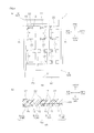
- FIG. 1 shows one embodiment of an element-connecting board of the present invention
- FIG. 2 shows a lead frame with a joint used in a method for producing the element-connecting board shown in FIG. 1 :
- FIG. 3 shows a lead frame with a joint used in a method for producing the element-connecting board shown in FIG. 1 and having spaces filled with a first insulating resin portion:
- FIG. 4 shows one embodiment of a light emitting diode device of the present invention
- FIG. 5 shows a front sectional view for illustrating a step of attaching an encapsulating sheet to the element-connecting board.
- FIG. 6 shows a front sectional view for illustrating another embodiment (an embodiment in which side surfaces of the lead frame are exposed) of the element-connecting board of the present invention.
- FIG. 7 shows a front sectional view for illustrating another embodiment (an embodiment in which second insulating resin portions are formed on the lower surface of the lead frame) of the element-connecting board of the present invention.
- FIG. 8 shows another embodiment of an element-connecting board of the present invention.
- FIG. 9 shows a lead frame used in a method for producing the element-connecting board shown in FIG. 8 :
- FIG. 10 shows another embodiment of a light emitting diode device of the present invention:
- FIG. 11 shows an embodiment of dividing the element-connecting board shown in FIG. 8 into two pieces:
- FIG. 1 shows one embodiment of an element-connecting board of the present invention.
- FIG. 2 shows a lead frame with a joint used in a method for producing the element-connecting board shown in FIG. 1 .
- FIG. 3 shows a lead frame with a joint used in a method for producing the element-connecting board shown in FIG. 1 and having spaces filled with a first insulating resin portion.
- the element-connecting board 1 is formed into a generally rectangular flat plate shape in plane view.
- the element-connecting board 1 includes a lead frame 4 which is provided with a plurality of leads 3 disposed with spaces 2 from each other (ref: FIGS. 2 ( a ) and 2 ( b )) and a first insulating resin portion 5 which is light reflective and fills the spaces 2 . Second insulating resin portions 6 are provided on the side surfaces of the element-connecting board 1 .
- the lead frame 4 is an electrically-conductive member for allowing light emitting diode elements 17 (ref: FIGS. 4 ( a ) and 4 ( b )) to be described later to be connected to the upper surface (one surface in the thickness direction) thereof.
- An example of a material which forms the lead frame 4 includes an electrically-conductive material such as copper, nickel, gold, and 42 alloy.
- a plurality of the leads 3 are defined by the spaces 2 extending along the front-rear direction (a direction perpendicular to the thickness direction, hereinafter the same). That is, a plurality of the leads 3 are formed into generally rectangular shapes in plane view extending in the front-rear direction and are disposed in alignment at spaced intervals to each other in the widthwise direction (the right-left direction).
- a plurality of the leads 3 include a first lead 8 and a second lead 9 which is adjacent to the first lead 8 in the widthwise direction.
- the first lead 8 is formed into a generally U-shaped shape in plane view which is open toward the rear side.
- the first lead 8 integrally includes a plurality (two pieces) of first linear portions 10 which are disposed in alignment at spaced intervals to each other in the widthwise direction and a first connecting portion 11 which connects the front end portions (one end portions) of the first linear portions 10 .
- Two pieces of the first linear portions 10 are formed into generally flat plate shapes extending in parallel in the front-rear direction.
- a first linear portion 10 B at the right side when projected in the widthwise direction, slightly protrudes toward the front side with respect to a first linear portion 10 A at the left side.
- first pads 12 which protrude from the both end surfaces in the widthwise direction partway in the front-rear direction thereof toward the both sides in the widthwise direction are provided.
- first pads 12 which protrude from the left end surface partway in the front-rear direction thereof toward the left side are provided.
- the first pads 12 are disposed in alignment at spaced intervals to each other in the front-rear direction.
- Each of the first pads 12 is formed into a generally rectangular shape in plane view extending in the widthwise direction.
- the first connecting portion 11 is disposed at the front end portion of the element-connecting board 1 and is formed into a generally rectangular shape in plane view extending in the right-left direction.
- the second lead 9 is formed into a point-symmetric shape obtained by rotating 180 degrees around the first lead 8 on the element-connecting board 1 .
- the second lead 9 is formed into a generally U-shaped shape in plane view which is open toward the front side.
- the second lead 9 integrally forms a plurality (two pieces) of second linear portions 13 which are disposed in alignment at spaced intervals to each other in the widthwise direction and a second connecting portion 14 which connects the rear end portions (the other end portions) of the second linear portions 13 .
- Two pieces of the second linear portions 13 are formed into generally flat plate shapes extending in parallel in the front-rear direction.
- a second linear portion 13 B at the left side when projected in the widthwise direction, slightly protrudes toward the front side with respect to a second linear portion 13 A at the right side.
- second pads 15 which protrude from the both end surfaces in the widthwise direction partway in the front-rear direction thereof toward the both sides in the widthwise direction are provided.
- the second pads 15 which protrude from the right end surface partway in the front-rear direction thereof toward the right side are provided.
- the second pads 15 are disposed in alignment at spaced intervals to each other in the front-rear direction.
- Each of the second pads 15 is formed into a generally rectangular shape in plane view extending in the widthwise direction.
- the second connecting portion 14 is disposed at the rear end portion of the element-connecting board 1 and is formed into a generally rectangular shape in plane view extending in the right-left direction.
- the first lead 8 and the second lead 9 are disposed in such a way that the first linear portions 10 and the second linear portions 13 are spaced in opposed relation to each other in the widthwise direction.
- two pieces of the first linear portions 10 and two pieces of the second linear portions 13 are alternately (by turns) arranged from the right side toward the left side.
- the first lead 8 and the second lead 9 are disposed so that each of the first linear portions 10 and each of the second linear portions 13 are alternately meshed (fitted) with each other with the spaces 2 therebetween. In this way, the first pads 12 and the second pads 15 are disposed in opposed relation to each other with spaces 2 therebetween in the widthwise direction.
- the first linear portion 10 A at the left side in the first lead 8 and the second connecting portion 14 in the second lead 9 are disposed with the space 2 therebetween in the front-rear direction.
- the second linear portion 13 A at the right side in the second lead 9 and the first connecting portion 11 in the first lead 8 are disposed with the space 2 therebetween in the front-rear direction.
- a thickness T 1 of the lead frame 4 is, for example, 35 to 2000 ⁇ m, or preferably 200 to 1000 ⁇ m.
- a width L 1 of each of the first linear portions 10 and each of the second linear portions 13 is, for example, 300 to 1800 ⁇ m, or preferably 800 to 1200 ⁇ m.
- a length L 2 in the front-rear direction of each of the first pads 12 and each of the second pads 15 is, for example, 500 to 3500 ⁇ m, or preferably 1000 to 3000 ⁇ m.
- a width L 3 of each of the first pads 12 and each of the second pads 15 is, for example, 1000 to 5000 ⁇ m, or preferably 3500 to 4500 ⁇ m.
- a gap L 4 in the front-rear direction between the first pads 12 and the gap L 4 in the front-rear direction between the second pads 15 are, for example, 3000 to 9000 ⁇ m, or preferably 5000 to 7000 ⁇ m.
- a length L 5 in the widthwise direction of the first connecting portion 11 and the second connecting portion 14 and the length L 7 in the front-rear direction of the first connecting portion 11 and the second connecting portion 14 are, for example, 15000 to 27000 ⁇ m, or preferably 18000 to 24000 ⁇ m.
- a width (a length in the widthwise direction) L 8 of the space 2 between the first pad 12 and the second pad 15 which are opposed to each other in the widthwise direction is, for example, 50 to 1000 ⁇ m, or preferably 100 to 400 ⁇ m.
- a width (a length in the widthwise direction) L 9 of the space 2 between the portion of each of the first linear portions 10 between the first pads 12 adjacent to each other in the front-rear direction and the portion of each of the second linear portions 13 between the second pads 15 adjacent to each other in the front-rear direction is, for example, 500 to 8000 ⁇ m, or preferably 1000 to 4000 ⁇ m.
- the first insulating resin portion 5 is, for example, in view of obtaining light reflectivity, formed from a reflecting resin composition.
- the reflecting resin composition contains, for example, an encapsulating resin composition and a light reflecting component.
- Examples of the encapsulating resin composition include a silicone resin composition and an epoxy resin composition.
- the silicone resin composition is a condensation and addition reaction curable type silicone resin composition which can undergo a condensation reaction and an addition reaction (to be specific, a hydrosilylation reaction).
- the silicone resin composition can be brought into a semi-cured (B-stage) state by undergoing the condensation reaction by heating and then, be brought into a cured (completely cured) state by undergoing the addition reaction by further heating.
- the silicone resin composition contains, for example, a polysiloxane containing silanol groups at both ends, an ethylenic silicon compound, a silicon compound containing an epoxy group, an organohydrogensiloxane, a condensation catalyst, and an addition catalyst.
- the polysiloxane containing silanol groups at both ends, the ethylenic silicon compound, and the silicon compound containing an epoxy group are condensation materials (materials subjected to the condensation reaction) and the ethylenic silicon compound and the organohydrogensiloxane are addition materials (materials subjected to the addition reaction).
- the polysiloxane containing silanol groups at both ends is an organosiloxane which contains silanol groups (SiOH groups) at both ends of a molecule and to be specific, is represented by the following general formula (1).
- R 1 represents a monovalent hydrocarbon group selected from a saturated hydrocarbon group and an aromatic hydrocarbon group.
- n represents an integer of 1 or more.
- examples of the saturated hydrocarbon group include a straight chain or branched chain alkyl group having 1 to 6 carbon atoms (such as a methyl group, an ethyl group, a propyl group, an isopropyl group, a butyl group, an isobutyl group, a pentyl group, and a hexyl group) and a cycloalkyl group having 3 to 6 carbon atoms (such as a cyclopentyl group and a cyclohexyl group).
- a straight chain or branched chain alkyl group having 1 to 6 carbon atoms such as a methyl group, an ethyl group, a propyl group, an isopropyl group, a butyl group, an isobutyl group, a pentyl group, and a hexyl group
- a cycloalkyl group having 3 to 6 carbon atoms such as a cyclopentyl group and
- an example of the aromatic hydrocarbon group includes an aryl group having 6 to 10 carbon atoms (such as a phenyl group and a naphthyl group).
- R 1 s may be the same or different from each other. Preferably, R 1 s are the same.
- the monovalent hydrocarbon group preferably, an alkyl group having 1 to 6 carbon atoms and an aryl group having 6 to 10 carbon atoms are used, or more preferably, in view of transparency, heat resistance, and light resistance, a methyl group is used.
- n is preferably, in view of stability and/or handling ability, an integer of 1 to 10,000, or more preferably an integer of 1 to 1,000.
- examples of the polysiloxane containing silanol groups at both ends include polydimethylsiloxane containing silanol groups at both ends, polymethylphenylsiloxane containing silanol groups at both ends, and polydiphenylsiloxane containing silanol groups at both ends.
- polysiloxanes containing silanol groups at both ends can be used alone or in combination.
- polysiloxanes containing silanol groups at both ends preferably, polydimethylsiloxane containing silanol groups at both ends is used.
- a commercially available product can be used as the polysiloxane containing silanol groups at both ends.
- a polysiloxane containing silanol groups at both ends synthesized in accordance with a known method can be also used.
- the number average molecular weight of the polysiloxane containing silanol groups at both ends is, in view of stability and/or handling ability, for example, 100 to 1,000,000, or preferably 200 to 100,000.
- the number average molecular weight is calculated by conversion based on standard polystyrene with a gel permeation chromatography.
- the number average molecular weight of materials, other than the polysiloxane containing silanol groups at both ends, to be described later, is also calculated in the same manner as described above.
- the content of the silanol group in the polysiloxane containing silanol groups at both ends is, for example, 0.002 to 25 mmol/g, or preferably 0.02 to 25 mmol/g.
- the content of the silanol group is calculated from the integral proportion of the peaks of the silanol group and the methyl group with a 1 H-NMR.
- the mixing ratio of the polysiloxane containing silanol groups at both ends with respect to 100 parts by mass of the condensation material is, for example, 1 to 99.99 parts by mass, preferably 50 to 99.9 parts by mass, or more preferably 80 to 99.5 parts by mass.
- the ethylenic silicon compound is a silane compound having both an ethylenically unsaturated hydrocarbon group and a leaving group in a silanol condensation reaction and to be specific, is represented by the following general formula (2).
- R 2 represents a monovalent ethylenically unsaturated hydrocarbon group.
- X 1 represents a halogen atom, an alkoxy group, a phenoxy group, or an acetoxy group. X 1 s may be the same or different from each other.
- an example of the ethylenically unsaturated hydrocarbon group represented by R 2 includes a substituted or unsubstituted ethylenically unsaturated hydrocarbon group.
- Examples thereof include an alkenyl group and a cycloalkenyl group.
- alkenyl group includes an alkenyl group having 2 to 10 carbon atoms such as a vinyl group, an allyl group, a propenyl group, a butenyl group, a pentenyl group, a hexenyl group, a heptenyl group, and an octenyl group.
- cycloalkenyl group includes a cycloalkenyl group having 3 to 10 carbon atoms such as a cyclohexenyl group and a norbornenyl group.
- an alkenyl group is used, more preferably, an alkenyl group having 2 to 5 carbon atoms is used, or particularly preferably, a vinyl group is used.
- X 1 in the above-described general formula (2) is a leaving group in the silanol condensation reaction.
- SiX 1 group in the above-described general formula (2) is a reactive functional group in the silanol condensation reaction.
- examples of a halogen atom represented by X 1 include bromine, chlorine, fluorine, and iodine.
- examples of the alkoxy group represented by X 1 include an alkoxy group containing a straight chain or branched chain alkyl group having 1 to 6 carbon atoms (such as a methoxy group, an ethoxy group, a propoxy group, an isopropoxy group, a butoxy group, an isobutoxy group, a pentyloxy group, and a hexyloxy group) and an alkoxy group containing a cycloalkyl group having 3 to 6 carbon atoms (such as a cyclopentyloxy group and a cyclohexyloxy group).
- X 1 s may be the same or different from each other. Preferably, X 1 s are the same.
- X 1 s in the above-described general formula (2) preferably, an alkoxy group is used, or more preferably, a methoxy group is used.
- Examples of the ethylenic silicon compound include a trialkoxysilane containing an ethylenically unsaturated hydrocarbon group, a trihalogenated silane containing an ethylenically unsaturated hydrocarbon group, a triphenoxysilane containing an ethylenically unsaturated hydrocarbon group, and a triacetoxysilane containing an ethylenically unsaturated hydrocarbon group.
- ethylenic silicon compounds can be used alone or in combination.
- a trialkoxysilane containing an ethylenically unsaturated hydrocarbon group is used.
- examples of the trialkoxysilane containing an ethylenically unsaturated hydrocarbon group include vinyltrialkoxysilane such as vinyltrimethoxysilane, vinyltriethoxysilane, and vinyltripropoxysilane; allyltrialkoxysilane such as allyltrimethoxysilane; propenyltrialkoxysilane such as propenyltrimethoxysilane; butenyltrialkoxysilane such as butenyltrimethoxysilane; and cyclohexenyltrialkoxysilane such as cyclohexenyltrimethoxysilane.
- vinyltrialkoxysilane such as vinyltrimethoxysilane, vinyltriethoxysilane, and vinyltripropoxysilane
- allyltrialkoxysilane such as allyltrimethoxysilane
- propenyltrialkoxysilane such as propenyltrimeth
- trialkoxysilanes containing an ethylenically unsaturated hydrocarbon group preferably, vinyltrialkoxysilane is used, or more preferably, vinyltrimethoxysilane is used.
- the mixing ratio of the ethylenic silicon compound with respect to 100 parts by mass of the condensation material is, for example, 0.01 to 90 parts by mass, preferably 0.01 to 50 parts by mass, or more preferably 0.01 to 10 parts by mass.
- a commercially available product can be used as the ethylenic silicon compound.
- An ethylenic silicon compound synthesized in accordance with a known method can be also used.
- the silicon compound containing an epoxy group is a silane compound having both an epoxy group and a leaving group in the silanol condensation reaction and to be specific, is represented by the following general formula (3).
- R 3 represents a group having an epoxy structure.
- X 2 represents a halogen atom, an alkoxy group, a phenoxy group, or an acetoxy group.
- X 2 s may be the same or different from each other.
- examples of the group having an epoxy structure represented by R 3 include an epoxy group, a glycidyl ether group, and an epoxycycloalkyl group such as an epoxycyclohexyl group.
- a glycidyl ether group is used.
- the glycidyl ether group is a glycidoxyalkyl group represented by the following general formula (4).
- R 4 represents a divalent hydrocarbon group selected from a saturated hydrocarbon group and an aromatic hydrocarbon group.
- examples of the saturated hydrocarbon group include an alkylene group having 1 to 6 carbon atoms (such as a methylene group, an ethylene group, a propylene group, and a butylene group) and a cycloalkylene group having 3 to 8 carbon atoms (such as a cyclopentylene group and a cyclohexylene group).
- an example of the aromatic hydrocarbon group includes an arylene group having 6 to 10 carbon atoms (such as a phenylene group and a naphthylene group).
- divalent hydrocarbon group preferably, an alkylene group having 1 to 6 carbon atoms is used, or more preferably, a propylene group is used.
- examples of the glycidyl ether group include a glycidoxymethyl group, a glycidoxyethyl group, a glycidoxypropyl group, a glycidoxycyclohexyl group, and a glycidoxyphenyl group.
- glycidyl ether groups preferably, a glycidoxypropyl group is used.
- X 2 in the above-described general formula (3) is a leaving group in the silanol condensation reaction.
- SiX 2 group in the above-described general formula (3) is a reactive functional group in the silanol condensation reaction.
- an example of the halogen atom represented by X 2 includes the same halogen atom as that represented by X 1 in the above-described general formula (2).
- an example of the alkoxy group represented by X 2 includes the same alkoxy group as that represented by X 1 in the above-described general formula (2).
- X 2 s may be the same or different from each other. Preferably, X 2 s are the same.
- X 2 in the above-described general formula (3) preferably, an alkoxy group is used, or more preferably, a methoxy group is used.
- Examples of the silicon compound containing an epoxy group include a trialkoxysilane containing an epoxy group, a trihalogenated silane containing an epoxy group, a triphenoxysilane containing an epoxy group, and a triacetoxysilane containing an epoxy group.
- the silicon compounds containing an epoxy group can be used alone or in combination.
- a trialkoxysilane containing an epoxy group is used.
- examples of the trialkoxysilane containing an epoxy group include glycidoxyalkyltrimethoxysilane such as glycidoxymethyltrimethoxysilane, (2-glycidoxyethyl)trimethoxysilane, and (3-glycidoxypropyl)trimethoxysilane; glycidoxyalkyltriethoxysilane such as (3-glycidoxypropyl)triethoxysilane; glycidoxyalkyltripropoxysilane such as (3-glycidoxypropyl)tripropoxysilane; and glycidoxyalkyltriisopropoxysilane such as (3-glycidoxypropyl)triisopropoxysilane.
- glycidoxyalkyltrimethoxysilane such as glycidoxymethyltrimethoxysilane, (2-glycidoxyethyl)trimethoxysilane, and (3-glycidoxypropyl)tri
- trialkoxysilanes containing an epoxy group preferably, glycidoxymethyltrialkoxysilane is used, or more preferably, (3-glycidoxypropyl)trimethoxysilane is used.
- the mixing ratio of the silicon compound containing an epoxy group with respect to 100 parts by mass of the condensation material is, for example, 0.01 to 90 parts by mass, preferably 0.01 to 50 parts by mass, or more preferably 0.01 to 1 parts by mass.
- a commercially available product can be used as the silicon compound containing an epoxy group.
- a silicon compound containing an epoxy group synthesized in accordance with a known method can be also used.
- the molar ratio (SiOH/(SiX 1 +SiX 2 )) of the silanol group (the SiOH group) in the polysiloxane containing silanol groups at both ends to the reactive functional group (the SiX 1 group and the SiX 2 group) in the ethylenic silicon compound and the silicon compound containing an epoxy group is, for example, 20/1 to 0.2/1, preferably 10/1 to 0.5/1, or more preferably substantially 1/1.
- the molar ratio exceeds the above-described range, there may be a case where a product in a semi-cured state (a semi-cured product) having an appropriate toughness is not obtained when the silicone resin composition is brought into a semi-cured state.
- the molar ratio is below the above-described range, the mixing proportion of the ethylenic silicon compound and the silicon compound containing an epoxy group is excessively large, so that the heat resistance of the first insulating resin portion 5 may be reduced.
- the silanol group (the SiOH group) in the polysiloxane containing silanol groups at both ends, and the reactive functional group (the SiX 1 group) in the ethylenic silicon compound and the reactive functional group (the SiX 2 group) in the silicon compound containing an epoxy group can be allowed to undergo the condensation reaction neither too much nor too little.
- the molar ratio of the ethylenic silicon compound to the silicon compound containing an epoxy group is, for example, 10/90 to 99/1, preferably 50/50 to 97/3, or more preferably 80/20 to 95/5.
- the organohydrogensiloxane is an organosiloxane having, in one molecule, at least two hydrosilyl groups (the SiH groups) without containing an ethylenically unsaturated hydrocarbon group.
- an example of the organohydrogensiloxane includes an organopolysiloxane such as an organopolysiloxane containing hydrogen atoms in its side chain and an organopolysiloxane containing hydrogen atoms at both ends.
- the organopolysiloxane containing hydrogen atoms in its side chain is an organohydrogenpolysiloxane having hydrogen atoms as a side chain which branches off from the main chain and is represented by formula (5).
- R 5 represents a monovalent hydrocarbon group selected from a saturated hydrocarbon group and an aromatic hydrocarbon group. “b” represents an integer of 0 or more and “c” represents an integer of 1 or more.)
- a to D constitute an organopolysiloxane containing a hydrogen atom in its side chain.
- the monovalent hydrocarbon groups represented by R 5 in formula (5) may be the same or different from each other.
- the monovalent hydrocarbon groups represented by R 5 are the same.
- examples of the saturated hydrocarbon group and the aromatic hydrocarbon group include the same saturated hydrocarbon group and aromatic hydrocarbon group as those illustrated by R 1 in the above-described general formula (1).
- the monovalent hydrocarbon group preferably, methyl and phenyl are used, or more preferably, methyl is used.
- “b” is preferably, in view of reactivity and stability, an integer of 1 to 10,000, more preferably an integer of 2 to 5,000, or particularly preferably an integer of 5 to 100.
- “c” is preferably 2 or more, in view of reactivity and stability, preferably an integer of 1 to 10,000, more preferably an integer of 2 to 1,000, or particularly preferably an integer of 5 to 100.
- organopolysiloxane containing hydrogen atoms in its side chain examples include methylhydrogenpolysiloxane, dimethylpolysiloxane-co-methylhydrogenpolysiloxane, ethylhydrogenpolysiloxane, and methylhydrogenpolysiloxane-co-methylphenylpolysiloxane.
- the number average molecular weight of the organopolysiloxane containing hydrogen atoms in its side chain is, for example, 100 to 1,000,000.
- the organopolysiloxane containing hydrogen atoms at both ends is an organohydrogenpolysiloxane having hydrogen atoms at both ends of the main chain and is represented by formula (6).
- R 6 represents a monovalent hydrocarbon group selected from a saturated hydrocarbon group and an aromatic hydrocarbon group. “d” represents an integer of 1 or more.
- examples of the saturated hydrocarbon group and the aromatic hydrocarbon group include the same saturated hydrocarbon group and aromatic hydrocarbon group as those illustrated by R 1 in the above-described general formula (1).
- the monovalent hydrocarbon group preferably, methyl and phenyl are used, or more preferably, methyl is used.
- “d” is preferably, in view of reactivity and stability, an integer of 1 to 10,000, or more preferably an integer of 1 to 5,000.
- organopolysiloxane containing hydrogen atoms at both ends examples include polydimethylsiloxane containing hydrosilyl groups at both ends, polymethylphenylsiloxane containing hydrosilyl groups at both ends, and polydiphenylsiloxane containing hydrosilyl groups at both ends.
- the number average molecular weight of the organopolysiloxane containing hydrogen atoms at both ends is, for example, in view of stability and/or handling ability, 100 to 1,000,000, or preferably 100 to 100,000.
- organohydrogensiloxanes can be used alone or in combination.
- organohydrogensiloxanes preferably, an organopolysiloxane containing hydrogen atoms in its side chain is used, or more preferably, dimethylpolysiloxane-co-methylhydrogenpolysiloxane is used.
- the viscosity of the organohydrogensiloxane at 25° C. is, for example, 10 to 100,000 mPa ⁇ s, or preferably 20 to 50,000 mPa ⁇ s.
- the viscosity is measured using a B-type viscometer.
- the content of the hydrosilyl group in the organohydrogensiloxane is, for example, 0.1 to 15 mmol/g, or preferably 0.5 to 10 mmol/g.
- the content of the hydrosilyl group is calculated from the integral proportion of the peaks of the hydrosilyl group and the methyl group with a 1 H-NMR.
- organohydrogensiloxane A commercially available product can be used as the organohydrogensiloxane.
- An organohydrogensiloxane synthesized in accordance with a known method can be also used.
- the mixing ratio of the organohydrogensiloxane with respect to 100 parts by mass of the ethylenic silicon compound is, though depending on the molar ratio of the ethylenically unsaturated hydrocarbon group (R 2 in the above-described general formula (2)) in the ethylenic silicon compound to the hydrosilyl group (the SiH group) in the organohydrogensiloxane, for example, 10 to 10,000 parts by mass, or preferably 100 to 1,000 parts by mass.
- the molar ratio (R 2 /SiH) of the ethylenically unsaturated hydrocarbon group (R 2 in the above-described general formula (2)) in the ethylenic silicon compound to the hydrosilyl group (the SiH group) in the organohydrogensiloxane is, for example, 20/1 to 0.05/1, preferably 20/1 to 0.1/1, more preferably 10/1 to 0.1/1, particularly preferably 10/1 to 0.2/1, or most preferably 5/1 to 0.2/1.
- the molar ratio thereof can be also set to be, for example, less than 1/1 and not less than 0.05/1.
- the molar ratio exceeds 20/1, there may be a case where a semi-cured product having an appropriate toughness is not obtained when the silicone resin composition is brought into a semi-cured state.
- the molar ratio is below 0.05/1, the mixing proportion of the organohydrogensiloxane is excessively large, so that the heat resistance and the toughness of the first insulating resin portion 5 may be insufficient.
- the silicone resin composition in allowing the silicone resin composition to be in a semi-cured state, the silicone resin composition can be quickly transferred into a semi-cured state with respect to the silicone resin composition whose molar ratio is 20/1 to 1/1.
- the condensation catalyst is not particularly limited as long as it is a substance capable of improving the reaction rate of the condensation reaction of the silanol group and the reactive functional group (the SiX 1 group in the above-described general formula (2) and the SiX 2 group in the above-described general formula (3)).
- the condensation catalyst include an acid such as hydrochloric acid, acetic acid, formic acid, and sulfuric acid; a base such as potassium hydroxide, sodium hydroxide, potassium carbonate, and tetramethylammonium hydroxide; and a metal such as aluminum, titanium, zinc, and tin.
- condensation catalysts can be used alone or in combination.
- condensation catalysts in view of compatibility and thermal decomposition characteristics, preferably, a base is used, or more preferably, tetramethylammonium hydroxide is used.
- the mixing ratio of the condensation catalyst with respect to 100 mol of the polysiloxane containing silanol groups at both ends is, for example, 0.1 to 50 mol, or preferably 0.25 to 5 mol.
- the addition catalyst is not particularly limited as long as it is a substance (a hydrosilylation catalyst) capable of improving the reaction rate of the addition reaction, that is, the hydrosilylation reaction of the ethylenically unsaturated hydrocarbon group and the hydrosilyl group (the SiH group) and a metal catalyst is, for example, used.
- a hydrosilylation catalyst capable of improving the reaction rate of the addition reaction, that is, the hydrosilylation reaction of the ethylenically unsaturated hydrocarbon group and the hydrosilyl group (the SiH group) and a metal catalyst is, for example, used.
- the metal catalyst include a platinum catalyst such as platinum black, platinum chloride, chloroplatinic acid, a platinum olefin complex, a platinum carbonyl complex, and platinum acetyl acetate; a palladium catalyst; and a rhodium catalyst.
- a platinum catalyst is used, or more preferably, a platinum olefin complex is used.
- a platinum-divinylsiloxane complex such as a platinum-1,3-divinyl-1,1,3,3-tetramethyldisiloxane complex is used.
- a platinum catalyst is used, or more preferably, a platinum-carbonyl complex is used.
- the mixing ratio of the addition catalyst with respect to 100 parts by mass of the organohydrogensiloxane is, as a number of parts by mass of the metal amount in the addition catalyst, for example 1.0 ⁇ 10 ⁇ 4 to 1.0 parts by mass, preferably 1.0 ⁇ 10 ⁇ 4 to 0.5 parts by mass, or more preferably 1.0 ⁇ 10 ⁇ 4 to 0.05 parts by mass.
- condensation catalyst and addition catalyst a condensation catalyst and an addition catalyst in a solid state can be used as they are.
- a condensation catalyst and an addition catalyst can be used as a solution or as a dispersion liquid dissolved or dispersed in a solvent.
- the solvent examples include water; an alcohol such as methanol and ethanol; and an aromatic hydrocarbon such as toluene.
- a polysiloxane containing silanol groups at both ends, an ethylenic silicon compound, a silicon compound containing an epoxy group, an organohydrogensiloxane, a condensation catalyst, and an addition catalyst are blended to be stirred and mixed, so that the silicone resin composition is prepared.
- the above-described materials (the condensation materials and the addition materials) and the catalysts can be blended simultaneously.
- each of the materials and each of the catalysts can be blended, respectively, at different timings.
- a part of the components can be added simultaneously and each of the remaining components can be blended, respectively, at different timings.
- the condensation materials are first prepared and then, the condensation catalyst is blended into the prepared condensation materials to prepare a mixture.
- the addition material is blended into the prepared mixture and then, the addition catalyst is blended thereto.
- the condensation catalyst is blended thereto to be stirred and mixed for, for example, 5 minutes to 24 hours, so that a mixture is prepared.
- the temperature can be also adjusted to be, for example, 0 to 60° C. so as to improve the compatibility and the handling ability of the condensation materials.
- the condensation reaction of the SiOH group in the polysiloxane containing silanol groups at both ends, and the SiX 1 group in the ethylenic silicon compound and the SiX 2 group in the silicon compound containing an epoxy group may be partially initiated.
- the degree of progress of the condensation reaction can be checked by 1 H-NMR measurement based on the disappearance degree of the peak derived from the SiOH group.
- the organohydrogensiloxane is blended into the prepared mixture of the condensation materials and the condensation catalyst to be stirred for, for example, 1 to 120 minutes.
- the temperature can be also adjusted to be, for example, 0 to 60° C. so as to improve the compatibility and the handling ability of the mixture and the organohydrogensiloxane.
- the addition catalyst is blended into the system (the above-described mixture) to be stirred for, for example, 1 to 60 minutes.
- the silicone resin composition is prepared.
- the silicone resin composition is, for example, in a liquid state (in an oil state). Although described later, after the preparation thereof, the silicone resin composition is prepared as an encapsulating resin composition by blending a light reflecting component and the like thereto. Thereafter, the encapsulating resin composition in a liquid state or in a semi-solid state fills the spaces 2 . Then, the encapsulating resin composition is heated, so that the condensation materials are subjected to a condensation reaction to be brought into a B-stage state (a semi-cured state). Thereafter, by further heating, the addition material is subjected to an addition reaction to be brought into a C-stage state (a completely cured state).
- the epoxy resin composition is a resin composition which is capable of thermally curing by heating.
- the epoxy resin composition is not particularly limited. Examples thereof include a thermosetting resin which contains an epoxy resin, a curing agent, and a curing accelerator described in Japanese Unexamined Patent Publication No. 2011-119393 and an insulating resin layer forming material which contains an epoxy resin and an acid anhydride curing agent described in Japanese Unexamined Patent Publication No. 2011-60819.
- the mixing proportion of the epoxy resin, the curing agent, and the curing accelerator in the thermosetting resin is set in conformity with, for example, the description in Japanese Unexamined Patent Publication No. 2011-119393.
- the mixing proportion of the epoxy resin and the acid anhydride curing agent in the insulating resin layer forming material is set in conformity with, for example, the description in Japanese Unexamined Patent Publication No. 2011-60819.
- the content ratio of the encapsulating resin compositions with respect to the reflecting resin composition is, for example, 10 to 99.5 mass %, preferably, in view of coloring characteristics and handling ability of the reflecting resin composition, 30 to 98.5 mass %, or more preferably 40 to 60 mass %.
- encapsulating resin compositions can be used alone or in combination.
- a silicone resin composition is used as the encapsulating resin composition.
- the light reflecting component is, for example, a white compound.
- a white compound includes a white pigment.
- the white pigment includes a white inorganic pigment.
- the white inorganic pigment include an oxide such as titanium oxide, zinc oxide, and zirconium oxide; a carbonate such as white lead (lead carbonate) and calcium carbonate; and a clay mineral such as kaolin (kaolinite).
- an oxide is used, or more preferably, titanium oxide is used.
- the titanium oxide can have characteristics such as a high degree of whiteness, a high light reflectivity, excellent hiding characteristics (hiding power), excellent coloring characteristics (coloring power), a high dispersibility, an excellent weather resistance, and a high chemical stability.
- the titanium oxide is TiO 2 (titanium oxide (IV), titanium dioxide).
- a crystal structure of the titanium oxide is not particularly limited.
- Examples of the crystal structure thereof include a rutile type, a brookite type (pyromelane), and an anatase type (octahedrite).
- a rutile type is used.
- a crystal system of the titanium oxide is not particularly limited.
- Examples of the crystal system thereof include a tetragonal system and an orthorhombic system.
- Preferably, a tetragonal system is used.
- the crystal structure and the crystal system of the titanium oxide are the rutile type and the tetragonal system, respectively, it is possible to effectively prevent a reduction of the reflectivity with respect to light (to be specific, visible light, among all, the light around the wavelength of 450 nm) even in a case where the first insulating resin portion 5 is exposed to a high temperature for a long time.
- the light reflecting component is in the form of a particle.
- the shape thereof is not limited and examples of the shape thereof include a sphere shape, a plate shape, and a needle shape.
- An average value of the maximum length (in the case of the sphere shape, the average particle size) of the light reflecting component is in the range of, for example, 1 to 1,000 nm, or preferably 100 to 500 nm.
- the average value of the maximum length is measured by using a laser diffraction scattering particle size analyzer.
- the content ratio of the light reflecting component with respect to the reflecting resin composition is, for example, 0.5 to 90 mass %, preferably, in view of coloring characteristics and light reflectivity, and handling ability of the reflecting resin composition, 1.5 to 70 mass %, more preferably 10 to 40 mass %, or particularly preferably 25 to 35 mass %.
- the mixing ratio of the light reflecting component with respect to 100 parts by mass of the encapsulating resin composition is, for example, 2 to 200 parts by mass, preferably 10 to 90 parts by mass, or more preferably 25 to 75 parts by mass.
- the encapsulating resin composition and the light reflecting component are blended to be uniformly mixed, so that the reflecting resin composition is prepared.
- the light reflecting component is uniformly dispersed and mixed into the encapsulating resin composition.
- the reflecting resin composition can further contain an inorganic filler.
- examples of the inorganic filler include silica (silicon dioxide), barium sulfate, barium carbonate, barium titanate, magnesium oxide, iron oxide, aluminum hydroxide, calcium carbonate, layered mica, carbon black, diatomite, and glass fiber.
- These inorganic fillers can be used alone or in combination.
- silica silicon dioxide
- the inorganic filler is in the form of a particle.
- the shape thereof is not limited and examples of the shape thereof include a sphere shape, a plate shape, and a needle shape.
- An average value of the maximum length (in the case of the sphere shape, the average particle size) of the inorganic filler is in the range of, for example, 1 to 1,000 nm, or preferably 100 to 500 nm.
- the average value of the maximum length is measured by using a laser diffraction scattering particle size analyzer.
- the average particle size of the inorganic filler is in the range of, for example, 1 to 1,000 ⁇ m, or preferably 10 to 100 ⁇ m.
- the average value of the maximum length is measured by using a laser diffraction scattering particle size analyzer.
- the content ratio of the inorganic filler with respect to the reflecting resin composition is, for example, 1 to 50 mass %, preferably, 5 to 40 mass %, or more preferably 15 to 30 mass %.
- the total number of parts by mass of the light reflecting component and the inorganic filler with respect to 100 parts by mass of the encapsulating resin composition is, for example, 50 to 300 parts by mass, or preferably 100 to 200 parts by mass.
- the mass ratio (mass of light reflecting component/(mass of light reflecting component+mass of inorganic filler)) of the light reflecting component with respect to the total number of parts by mass of the light reflecting component and the inorganic filler is, for example, 0.0001 to 1, or preferably 0.01 to 1.
- the mass ratio (mass of light reflecting component/mass of inorganic filler) of the light reflecting component with respect to the inorganic filler is, for example, 0.2 to 3.0, or preferably 0.5 to 2.0.
- the mass ratio (mass of light reflecting component/mass of inorganic filler) of the light reflecting component with respect to the inorganic filler is, for example, 0.26 to 3.0.
- the above-described inorganic filler is uniformly dispersed and mixed into the encapsulating resin composition together with the light reflecting component.
- the reflecting resin composition prepared in this way is prepared in a liquid state or in a semi-solid state.
- the first insulating resin portion 5 is formed so that all of the upper surfaces and the lower surfaces of a plurality of the leads 3 are exposed.
- the first insulating resin portion 5 fills the spaces 2 which are defined in the widthwise direction by the first pads 12 and the second pads 15 that are opposed to each other in the widthwise direction.
- the first insulating resin portion 5 also fills the spaces 2 which are defined in the widthwise direction by the first linear portions 10 between each of the first pads 12 that are adjacent to each other in the front-rear direction and by the second linear portions 13 between each of the second pads 15 that are adjacent to each other in the front-rear direction.
- the first insulating resin portion 5 does not fill the space 2 defined by the first connecting portion 11 of the first lead 8 , and the first pads 12 and the second pads 15 which are disposed in opposed relation to each other at the rear side of the first connecting portion 11 .
- Such a space 2 is defined as an empty space.
- the first insulating resin portion 5 also does not fill the space 2 defined by the second connecting portion 14 of the second lead 9 , and the first pads 12 and the second pads 15 which are disposed in opposed relation to each other at the front side of the second connecting portion 14 .
- Such a space 2 is defined as an empty space.
- a thickness T 2 of the first insulating resin portion 5 is substantially the same as the thickness T 1 of the lead frame 4 .
- the second insulating resin portion 6 is formed from, for example, the same reflecting resin composition as that of the first insulating resin portion 5 .
- the second insulating resin portion 6 can be also formed from, for example, an acrylic resin, a polyimide resin, or the like. In view of reducing the number of steps of the production process, preferably, the second insulating resin portion 6 is formed from the same reflecting resin composition as that of the first insulating resin portion 5 .
- the second insulating resin portions 6 are formed into generally flat plate shapes in plane view extending in the front-rear direction. To be specific, each of the second insulating resin portions 6 is formed along the right side surface of the first linear portion 10 A at the right side of the first lead 8 and is also formed along the left side surface of the second linear portion 13 B at the left side of the second lead 9 .
- a thickness T 3 of each of the second insulating resin portions 6 is substantially the same as the thickness T 1 of the lead frame 4 .
- the lead frame 4 , the first insulating resin portion 5 , and the second insulating resin portions 6 are formed to be flush with each other on the upper surfaces and the lower surfaces.
- a lead frame 4 ′ with a joint in which a plurality of the leads 3 are connected by a joint 16 is prepared.
- the lead frame 4 ′ with a joint is integrally provided with the above-described plurality of the leads 3 and the joint 16 which connect a plurality of the leads 3 .
- the joint 16 connects the first lead 8 and the second lead 9 . To be specific, the joint 16 connects the rear end portion of each of the first linear portions 10 with the second connecting portion 14 and also connects the front end portion of each of the second linear portions 13 with the first connecting portion 11 .
- the lead frame 4 ′ with a joint is formed into a generally rectangular flat plate shape in plane view.
- a flat plate (a metal plate) formed of the above-described conductive material is subjected to a punching process in which a stamping method is performed using a metal mold that corresponds to the spaces 2 or an etching process to form the spaces 2 , so that the lead frame 4 ′ with a joint is prepared.
- the light reflective first insulating resin portion 5 fills the spaces 2 .
- the second insulating resin portions 6 are formed on the side surfaces of the element-connecting board 1 .
- the above-described reflecting resin composition fills the spaces 2 by a forming process such as a transfer forming, a compression forming, a thermal press forming, or a lamination forming to form the first insulating resin portion 5 and the reflecting resin composition is applied to the side surfaces of the lead frame 4 to form the second insulating resin portions 6 .
- the reflecting resin composition is heated, so that when the reflecting resin composition contains a silicone resin composition, it is brought into a B-stage state (a semi-cured state).
- a structure which is provided with the lead frame 4 ′ with a joint, the first insulating resin portion 5 filling the spaces 2 of the lead frame 4 ′ with a joint, and the second insulating resin portions 6 formed on the side surfaces of the lead frame 4 ′ with a joint can be obtained as the element-connecting board 1 before the joint 16 is cut off.
- the joint 16 is removed by, for example, a punching process or an etching process.
- the lead frame 4 which is provided with the first lead 8 and the second lead 9 is formed. That is, a circuit in which the first lead 8 and the second lead 9 are electrically insulated from each other is formed.
- the element-connecting board 1 can be obtained.
- FIG. 4 shows one embodiment of a light emitting diode device of the present invention.
- FIG. 5 shows a front sectional view for illustrating a step of attaching an encapsulating sheet to the element-connecting board.
- FIG. 4 ( a ) an encapsulating sheet 19 is omitted so as to clearly show the relative arrangement of the lead frame 4 and the light emitting diode elements 17 .
- the light emitting diode elements 17 are connected to the element-connecting board 1 .
- the light emitting diode device 18 includes the element-connecting board 1 , the light emitting diode elements 17 connected to the upper surface (one surface in the thickness direction) of the element-connecting board 1 , and the encapsulating sheet 19 (ref: FIG. 4 ( b )) encapsulating the light emitting diode elements 17 .
- a plurality of the light emitting diode elements 17 are provided and to be specific, are mounted on the upper surfaces (one surface in the thickness direction) of the second pads 15 of the second lead 9 .
- the lower surfaces of the light emitting diode elements 17 are adhered to the upper surfaces of the second pads 15 via an electrically-conductive adhesive layer which is not shown. That is, the lower surfaces of the light emitting diode elements 17 are electrically connected to the upper surface of the second lead 9 .
- the light emitting diode elements 17 are electrically connected to the upper surfaces of the first pads 12 of the first lead 8 via wires 22 connected to the upper surfaces of the light emitting diode elements 17 . That is, the upper surfaces of the light emitting diode elements 17 are electrically connected to the first pads 12 which are disposed in opposed relation to the second pads 15 in the widthwise direction on which the light emitting diode elements 17 are mounted. That is, the upper surfaces of the light emitting diode elements 17 are electrically connected to the upper surface of the first lead 8 .
- the encapsulating sheet 19 is formed into a generally rectangular shape in plane view and is formed on (at one side in the thickness direction of) the element-connecting board 1 .
- An example of the encapsulating sheet 19 includes an encapsulating sheet described in Japanese Unexamined Patent Publication No. 2011-159874.
- the element-connecting board 1 shown in FIGS. 1 ( a ) and 1 ( b ) is prepared.
- the light emitting diode elements 17 are connected to a plurality of the leads 3 .
- the encapsulating sheet 19 is disposed at the upper side of the light emitting diode elements 17 and the wires 22 so as to be overlapped with at least the light emitting diode elements 17 and the wires 22 when projected in the thickness direction. Subsequently, as shown by arrows in FIG.
- the encapsulating sheet 19 is attached to the element-connecting board 1 so as to embed the light emitting diode elements 17 and the wires 22 to be thereafter heated.
- the first insulating resin portion 5 and the second insulating resin portions 6 are prepared from the reflecting resin composition (the encapsulating resin composition)
- the first insulating resin portion 5 and the second insulating resin portions 6 are brought into a C-stage state (a completely cured state).
- each of the first lead 8 and the second lead 9 is connected to a power source 21 via power distribution lines 20 .
- the first insulating resin portion 5 fills the spaces 2 of the lead frame 4 , so that both of the upper surface of the lead frame 4 and the upper surface of the first insulating resin portion 5 can be exposed.
- the light emitting diode elements 17 are connected to the upper side of the lead frame 4 , thereafter, the light emitting diode elements 17 are easily and surely covered with the encapsulating sheet 19 , so that the light emitting diode elements 17 can be easily and surely encapsulated.
- the first insulating resin portion 5 has light reflectivity, so that the element-connecting board 1 has an excellent light reflectivity. Therefore, in the light emitting diode device 18 including the element-connecting board 1 , light emitted from the light emitting diode elements 17 can be reflected, so that the luminous efficiency can be improved.
- the first insulating resin portion 5 fills the spaces 2 separating a plurality of the leads 3 , so that a plurality of the leads 3 can be surely supported to be reinforced.
- the side surfaces of the lead frame 4 can be laterally supported to be reinforced by the second insulating resin portions 6 .
- the light emitting diode elements 17 connected to the element-connecting board 1 can be easily and surely encapsulated by the above-described encapsulating sheet 19 . Therefore, the reliability of the light emitting diode device 18 can be easily and surely improved.
- the shape of the lead frame 4 ′ with a joint in which a plurality of the leads 3 are connected by the joint 16 is maintained, and the first insulating resin portion 5 surely fills the spaces 2 of the lead frame 4 ′ with a joint and a plurality of the leads 3 can be surely supported.
- a desired circuit consisting of a plurality of the leads 3 can be formed.
- FIG. 6 shows a front sectional view for illustrating another embodiment (an embodiment in which side surfaces of the lead frame are exposed) of the element-connecting board of the present invention.
- FIG. 7 shows a front sectional view for illustrating another embodiment (an embodiment in which second insulating resin portions are formed on the lower surface of the lead frame) of the element-connecting board of the present invention.
- FIG. 8 shows another embodiment of an element-connecting board of the present invention.
- FIG. 9 shows a lead frame used in a method for producing the element-connecting board shown in FIG. 8 .
- FIG. 10 shows another embodiment of a light emitting diode device of the present invention.
- FIG. 11 shows an embodiment of dividing the element-connecting board shown in FIG. 8 into two pieces.
- the second insulating resin portions 6 are formed on the side surfaces of the lead frame 4 .
- the second insulating resin portions 6 are not formed on the side surfaces of the lead frame 4 and the side surfaces of the lead frame 4 can be exposed.
- the lower surface (the other surface in the thickness direction) of the lead frame 4 is exposed.
- the lower surface of the lead frame 4 can be covered with the second insulating resin portions 6 .
- the second insulating resin portions 6 are provided on the portions of the lower surface of the lead frame 4 in addition to the side surfaces thereof. That is, the second insulating resin portions 6 are provided on the lower surface of the lead frame 4 at the both end portions in the widthwise direction.
- each of the second insulating resin portions 6 provided on the lower surface of the lead frame 4 is continuously formed on the lower surface of the first linear portion 10 B at the right side, the lower surface of the second linear portion 13 A at the right side, and the lower surface of the second insulating resin portion 6 which fills the space 2 between the first linear portion 10 B at the right side and the second linear portion 13 A at the right side.
- each of the second insulating resin portions 6 provided on the lower surface of the lead frame 4 is continuously formed on the lower surface of the second linear portion 13 B at the left side, the lower surface of the first linear portion 10 A at the left side, and the lower surface of the second insulating resin portion 6 which fills the space 2 between the second linear portion 13 B at the left side and the first linear portion 10 A at the left side.
- a thickness T 4 of each of the second insulating resin portions 6 provided on the lower surface of the lead frame 4 is, for example, 50 to 2000 ⁇ m, or preferably 100 to 300 ⁇ m.
- the embodiment in FIG. 7 can achieve the same function and effect as that of the embodiment in FIG. 1 .
- the lead frame 4 can be supported from below to be reinforced.
- each of the first lead 8 and the second lead 9 is provided with the first pads 12 and the second pads 15 .
- the first lead 8 and the second lead 9 can be formed without providing the first pads 12 and the second pads 15 .
- the element-connecting board 1 includes the lead frame 4 which is provided with a plurality of the leads 3 , the first insulating resin portion 5 which is light reflective and fills the spaces 2 , and the second insulating resin portions 6 which are formed on the side surfaces of the lead frame 4 .
- a plurality of the leads 3 include the first lead 8 disposed at the center in the widthwise direction and the second leads 9 each of which is disposed in opposed relation to the first lead 8 with the spaces 2 therebetween at the both outer sides in the widthwise direction of the first lead 8 .
- the first lead 8 is formed into a generally wide rectangular shape in plane view extending in the front-rear direction.
- Each of the second leads 9 is narrower than the first lead 8 and is formed into a generally rectangular shape in plane view extending long in the front-rear direction.
- the first insulating resin portion 5 fills the spaces 2 which are formed between the first lead 8 and each of the second leads 9 .
- the second insulating resin portions 6 are formed at the outer side surfaces in the widthwise direction of each of the second leads 9 .
- the lead frame 4 shown in FIGS. 9 ( a ) and 9 ( b ) is prepared.
- each of the both end portions in the front-rear direction of the first lead 8 is connected to each of the both end portions in the front-rear direction of each of the second leads 9 by a joint which is not shown.
- the resulting lead frame 4 is defined as the lead frame 4 ′ with a joint.
- the first insulating resin portion 5 and the second insulating resin portions 6 are formed from the reflecting resin composition.
- the light emitting diode elements 17 are connected to the element-connecting board 1 to constitute the light emitting diode device 18 .
- the light emitting diode elements 17 are provided at the both end portions in the widthwise direction of the first lead 8 and are disposed at spaced intervals to each other along the front-rear direction of the first lead 8 .
- the light emitting diode elements 17 are adhered to the upper surface of the first lead 8 via an electrically-conductive adhesive layer which is not shown. In this way, the light emitting diode elements 17 are electrically connected to the upper surface of the first lead 8 .
- the light emitting diode elements 17 are electrically connected to the upper surfaces of the second leads 9 via the wires 22 connected to the upper surfaces of the light emitting diode elements 17 . That is, the upper surfaces of the light emitting diode elements 17 are electrically connected to the upper surfaces of the second leads 9 .
- each of the light emitting diode elements 17 and the wires 22 can be also connected to the upper surfaces of the first lead 8 and the second leads 9 . Therefore, in the light emitting diode device 18 , the lead frame 4 includes the first lead 8 and the second leads 9 in the above-described shapes, so that a simple structure can be achieved.
- the size of the element-connecting board 1 in FIG. 8 can be appropriately selected.
- the element-connecting boards 1 can be also divided into a plurality of pieces (two pieces) so as to be divided in the front-rear direction by a cutting plane line CL 2 shown by a dashed line in FIG. 11 ( a ) by a cutting process such as a dicing method.
Landscapes
- Engineering & Computer Science (AREA)
- Microelectronics & Electronic Packaging (AREA)
- Manufacturing & Machinery (AREA)
- Computer Hardware Design (AREA)
- Power Engineering (AREA)
- General Engineering & Computer Science (AREA)
- Led Device Packages (AREA)
Priority Applications (1)
| Application Number | Priority Date | Filing Date | Title |
|---|---|---|---|
| US14/315,948 US8975101B2 (en) | 2011-11-30 | 2014-06-26 | Element connecting board, producing method thereof, and light emitting diode device |
Applications Claiming Priority (2)
| Application Number | Priority Date | Filing Date | Title |
|---|---|---|---|
| JP2011-261702 | 2011-11-30 | ||
| JP2011261702A JP5865038B2 (ja) | 2011-11-30 | 2011-11-30 | 素子接続用基板、その製造方法および発光ダイオード装置 |
Related Child Applications (1)
| Application Number | Title | Priority Date | Filing Date |
|---|---|---|---|
| US14/315,948 Continuation US8975101B2 (en) | 2011-11-30 | 2014-06-26 | Element connecting board, producing method thereof, and light emitting diode device |
Publications (2)
| Publication Number | Publication Date |
|---|---|
| US20130134467A1 US20130134467A1 (en) | 2013-05-30 |
| US8872211B2 true US8872211B2 (en) | 2014-10-28 |
Family
ID=47325897
Family Applications (2)
| Application Number | Title | Priority Date | Filing Date |
|---|---|---|---|
| US13/690,494 Expired - Fee Related US8872211B2 (en) | 2011-11-30 | 2012-11-30 | Element-connecting board, producing method thereof, and light-emitting diode device |
| US14/315,948 Expired - Fee Related US8975101B2 (en) | 2011-11-30 | 2014-06-26 | Element connecting board, producing method thereof, and light emitting diode device |
Family Applications After (1)
| Application Number | Title | Priority Date | Filing Date |
|---|---|---|---|
| US14/315,948 Expired - Fee Related US8975101B2 (en) | 2011-11-30 | 2014-06-26 | Element connecting board, producing method thereof, and light emitting diode device |
Country Status (6)
| Country | Link |
|---|---|
| US (2) | US8872211B2 (ja) |
| EP (1) | EP2600428A3 (ja) |
| JP (1) | JP5865038B2 (ja) |
| KR (1) | KR20130061108A (ja) |
| CN (2) | CN202957297U (ja) |
| TW (2) | TW201639200A (ja) |
Families Citing this family (10)
| Publication number | Priority date | Publication date | Assignee | Title |
|---|---|---|---|---|
| US10043960B2 (en) * | 2011-11-15 | 2018-08-07 | Cree, Inc. | Light emitting diode (LED) packages and related methods |
| JP5865038B2 (ja) * | 2011-11-30 | 2016-02-17 | 日東電工株式会社 | 素子接続用基板、その製造方法および発光ダイオード装置 |
| JP2015130476A (ja) * | 2013-12-04 | 2015-07-16 | 日東電工株式会社 | 光半導体装置用エポキシ樹脂組成物およびそれを用いて得られる光半導体装置用リードフレーム、封止型光半導体素子ならびに光半導体装置 |
| TW201639201A (zh) * | 2015-04-20 | 2016-11-01 | 億光電子工業股份有限公司 | 發光模組 |
| TWI569481B (zh) * | 2015-07-22 | 2017-02-01 | 友嘉科技股份有限公司 | 次黏著基板陣列 |
| EP3451394B1 (en) * | 2016-04-26 | 2021-01-06 | Citizen Electronics Co., Ltd. | Light-emitting device |
| CN107994109A (zh) * | 2016-10-27 | 2018-05-04 | 佛山市国星光电股份有限公司 | 一种cob显示模组及其制造方法 |
| TWI634679B (zh) * | 2017-03-27 | 2018-09-01 | 隆達電子股份有限公司 | 發光二極體裝置及其支架 |
| CN111373852B (zh) * | 2017-12-04 | 2021-10-22 | 株式会社富士 | 电子元件安装方向确认系统及电子元件安装方向确认方法 |
| US10862015B2 (en) | 2018-03-08 | 2020-12-08 | Samsung Electronics., Ltd. | Semiconductor light emitting device package |
Citations (8)
| Publication number | Priority date | Publication date | Assignee | Title |
|---|---|---|---|---|
| JPH07288341A (ja) | 1994-04-18 | 1995-10-31 | Nichia Chem Ind Ltd | Ledディスプレイ |
| US20010042865A1 (en) * | 1997-01-15 | 2001-11-22 | Kabushiki Kaisha Toshiba | Semiconductor light emitting device and its manufacturing method |
| US20030006421A1 (en) | 2001-06-15 | 2003-01-09 | Takemasa Yasukawa | Light-emitting device |
| US20040217369A1 (en) * | 2001-04-09 | 2004-11-04 | Kabushiki Kaisha Toshiba | Light emitting device |
| US7161190B2 (en) * | 2004-08-02 | 2007-01-09 | Sharp Kabushiki Kaisha | Semiconductor light-emitting device and method of manufacturing the same |
| US7326041B2 (en) * | 2001-11-12 | 2008-02-05 | Sanyo Electric Co., Ltd. | Lead frame, resin sealing mold and method for manufacturing a semiconductor device using the same |
| US20080194055A1 (en) * | 2003-09-03 | 2008-08-14 | Matsushita Electric Industrial Co., Ltd. | Solid-state imaging device and method for manufacturing the same |
| US20110186893A1 (en) | 2010-02-02 | 2011-08-04 | Nitto Denko Corporation | Optical-semiconductor device |
Family Cites Families (10)
| Publication number | Priority date | Publication date | Assignee | Title |
|---|---|---|---|---|
| JPH0728834A (ja) | 1993-07-12 | 1995-01-31 | Sony Corp | 情報検索装置 |
| JP4205135B2 (ja) * | 2007-03-13 | 2009-01-07 | シャープ株式会社 | 半導体発光装置、半導体発光装置用多連リードフレーム |
| JP5233170B2 (ja) * | 2007-05-31 | 2013-07-10 | 日亜化学工業株式会社 | 発光装置、発光装置を構成する樹脂成形体及びそれらの製造方法 |
| KR101326888B1 (ko) * | 2007-06-20 | 2013-11-11 | 엘지이노텍 주식회사 | 반도체 발광소자 패키지 |
| JP2011060819A (ja) | 2009-09-07 | 2011-03-24 | Nitto Denko Corp | 光半導体素子収納用実装パッケージ用樹脂組成物およびそれを用いて得られる光半導体発光装置 |
| JP5381563B2 (ja) * | 2009-09-29 | 2014-01-08 | 凸版印刷株式会社 | 発光素子用リードフレーム基板の製造方法 |
| JP5397195B2 (ja) | 2009-12-02 | 2014-01-22 | 日立化成株式会社 | 光半導体素子搭載用基板の製造方法、及び、光半導体装置の製造方法 |
| JP2011151239A (ja) * | 2010-01-22 | 2011-08-04 | Toppan Printing Co Ltd | Led用リードフレーム及びledモジュールの製造方法 |
| JP5545246B2 (ja) * | 2010-03-30 | 2014-07-09 | 信越化学工業株式会社 | 樹脂組成物及び発光半導体素子用リフレクター、及び発光半導体装置 |
| JP5865038B2 (ja) * | 2011-11-30 | 2016-02-17 | 日東電工株式会社 | 素子接続用基板、その製造方法および発光ダイオード装置 |
-
2011
- 2011-11-30 JP JP2011261702A patent/JP5865038B2/ja not_active Expired - Fee Related
-
2012
- 2012-11-30 KR KR1020120137488A patent/KR20130061108A/ko not_active Application Discontinuation
- 2012-11-30 CN CN201220652194XU patent/CN202957297U/zh not_active Expired - Fee Related
- 2012-11-30 US US13/690,494 patent/US8872211B2/en not_active Expired - Fee Related
- 2012-11-30 TW TW105122495A patent/TW201639200A/zh unknown
- 2012-11-30 EP EP12194998.6A patent/EP2600428A3/en not_active Withdrawn
- 2012-11-30 CN CN201210507621.XA patent/CN103137845B/zh not_active Expired - Fee Related
- 2012-11-30 TW TW101145108A patent/TWI555156B/zh not_active IP Right Cessation
-
2014
- 2014-06-26 US US14/315,948 patent/US8975101B2/en not_active Expired - Fee Related
Patent Citations (9)
| Publication number | Priority date | Publication date | Assignee | Title |
|---|---|---|---|---|
| JPH07288341A (ja) | 1994-04-18 | 1995-10-31 | Nichia Chem Ind Ltd | Ledディスプレイ |
| US20010042865A1 (en) * | 1997-01-15 | 2001-11-22 | Kabushiki Kaisha Toshiba | Semiconductor light emitting device and its manufacturing method |
| US20040217369A1 (en) * | 2001-04-09 | 2004-11-04 | Kabushiki Kaisha Toshiba | Light emitting device |
| US20030006421A1 (en) | 2001-06-15 | 2003-01-09 | Takemasa Yasukawa | Light-emitting device |
| US7326041B2 (en) * | 2001-11-12 | 2008-02-05 | Sanyo Electric Co., Ltd. | Lead frame, resin sealing mold and method for manufacturing a semiconductor device using the same |
| US20080194055A1 (en) * | 2003-09-03 | 2008-08-14 | Matsushita Electric Industrial Co., Ltd. | Solid-state imaging device and method for manufacturing the same |
| US7161190B2 (en) * | 2004-08-02 | 2007-01-09 | Sharp Kabushiki Kaisha | Semiconductor light-emitting device and method of manufacturing the same |
| US20110186893A1 (en) | 2010-02-02 | 2011-08-04 | Nitto Denko Corporation | Optical-semiconductor device |
| JP2011159874A (ja) | 2010-02-02 | 2011-08-18 | Nitto Denko Corp | 光半導体装置 |
Non-Patent Citations (1)
| Title |
|---|
| Non-Final Office Action dated Aug. 18, 2014, issued from the U.S. Patent and Trademark Office in U.S. Appl. No. 14/315,948. |
Also Published As
| Publication number | Publication date |
|---|---|
| US8975101B2 (en) | 2015-03-10 |
| EP2600428A2 (en) | 2013-06-05 |
| JP2013115310A (ja) | 2013-06-10 |
| KR20130061108A (ko) | 2013-06-10 |
| CN103137845A (zh) | 2013-06-05 |
| CN103137845B (zh) | 2017-04-12 |
| TW201324722A (zh) | 2013-06-16 |
| TWI555156B (zh) | 2016-10-21 |
| EP2600428A3 (en) | 2015-07-29 |
| US20140329346A1 (en) | 2014-11-06 |
| TW201639200A (zh) | 2016-11-01 |
| US20130134467A1 (en) | 2013-05-30 |
| JP5865038B2 (ja) | 2016-02-17 |
| CN202957297U (zh) | 2013-05-29 |
Similar Documents
| Publication | Publication Date | Title |
|---|---|---|
| US8975101B2 (en) | Element connecting board, producing method thereof, and light emitting diode device | |
| US9246063B2 (en) | Phosphor encapsulating sheet, light emitting diode device, and producing method thereof | |
| US8723167B2 (en) | Reflecting material and light emitting diode device | |
| US8937329B2 (en) | Encapsulating sheet, light emitting diode device, and producing method thereof | |
| US8519422B2 (en) | Encapsulating sheet and optical semiconductor element device | |
| US8828753B2 (en) | Producing method of light emitting diode device | |
| US20150076552A1 (en) | Silicone resin composition, semi-cured material sheet, producing method of silicone cured material, light emitting diode device, and producing method thereof | |
| EP2674993A2 (en) | Encapsulating sheet, light emitting diode device, and producing method thereof | |
| US20120083056A1 (en) | Light emitting diode sealing member and method for producing light emitting diode device | |
| US8716412B2 (en) | Silicone resin composition, encapsulating layer, reflector, and optical semiconductor device | |
| US20130099395A1 (en) | Silicone resin composition, encapsulating layer, reflector, and optical semiconductor device | |
| US9153755B2 (en) | Silicone resin sheet, cured sheet, and light emitting diode device and producing method thereof | |
| US20140178678A1 (en) | Encapsulating sheet | |
| US8883950B2 (en) | Silicone resin composition, encapsulating material, and light emitting diode device | |
| JP2015128188A (ja) | キット | |
| US20140178677A1 (en) | Encapsulating sheet |
Legal Events
| Date | Code | Title | Description |
|---|---|---|---|
| AS | Assignment |
Owner name: NITTO DENKO CORPORATION, JAPAN Free format text: ASSIGNMENT OF ASSIGNORS INTEREST;ASSIGNORS:OOYABU, YASUNARI;FUKE, KAZUHIRO;TSUKAHARA, DAISUKE;AND OTHERS;SIGNING DATES FROM 20121109 TO 20121113;REEL/FRAME:029390/0622 |
|
| FEPP | Fee payment procedure |
Free format text: MAINTENANCE FEE REMINDER MAILED (ORIGINAL EVENT CODE: REM.) |
|
| LAPS | Lapse for failure to pay maintenance fees |
Free format text: PATENT EXPIRED FOR FAILURE TO PAY MAINTENANCE FEES (ORIGINAL EVENT CODE: EXP.); ENTITY STATUS OF PATENT OWNER: LARGE ENTITY |
|
| STCH | Information on status: patent discontinuation |
Free format text: PATENT EXPIRED DUE TO NONPAYMENT OF MAINTENANCE FEES UNDER 37 CFR 1.362 |
|
| FP | Lapsed due to failure to pay maintenance fee |
Effective date: 20181028 |