US8854731B2 - Carbon dioxide laser light optical component - Google Patents
Carbon dioxide laser light optical component Download PDFInfo
- Publication number
- US8854731B2 US8854731B2 US13/090,989 US201113090989A US8854731B2 US 8854731 B2 US8854731 B2 US 8854731B2 US 201113090989 A US201113090989 A US 201113090989A US 8854731 B2 US8854731 B2 US 8854731B2
- Authority
- US
- United States
- Prior art keywords
- optical component
- carbon dioxide
- laser light
- dioxide laser
- concave
- Prior art date
- Legal status (The legal status is an assumption and is not a legal conclusion. Google has not performed a legal analysis and makes no representation as to the accuracy of the status listed.)
- Expired - Fee Related, expires
Links
Images


Classifications
-
- G—PHYSICS
- G02—OPTICS
- G02B—OPTICAL ELEMENTS, SYSTEMS OR APPARATUS
- G02B5/00—Optical elements other than lenses
- G02B5/18—Diffraction gratings
- G02B5/1809—Diffraction gratings with pitch less than or comparable to the wavelength
-
- B23K26/0639—
-
- B—PERFORMING OPERATIONS; TRANSPORTING
- B23—MACHINE TOOLS; METAL-WORKING NOT OTHERWISE PROVIDED FOR
- B23K—SOLDERING OR UNSOLDERING; WELDING; CLADDING OR PLATING BY SOLDERING OR WELDING; CUTTING BY APPLYING HEAT LOCALLY, e.g. FLAME CUTTING; WORKING BY LASER BEAM
- B23K26/00—Working by laser beam, e.g. welding, cutting or boring
- B23K26/02—Positioning or observing the workpiece, e.g. with respect to the point of impact; Aligning, aiming or focusing the laser beam
- B23K26/06—Shaping the laser beam, e.g. by masks or multi-focusing
- B23K26/064—Shaping the laser beam, e.g. by masks or multi-focusing by means of optical elements, e.g. lenses, mirrors or prisms
-
- G—PHYSICS
- G02—OPTICS
- G02B—OPTICAL ELEMENTS, SYSTEMS OR APPARATUS
- G02B1/00—Optical elements characterised by the material of which they are made; Optical coatings for optical elements
- G02B1/10—Optical coatings produced by application to, or surface treatment of, optical elements
- G02B1/11—Anti-reflection coatings
- G02B1/113—Anti-reflection coatings using inorganic layer materials only
- G02B1/115—Multilayers
-
- G—PHYSICS
- G02—OPTICS
- G02B—OPTICAL ELEMENTS, SYSTEMS OR APPARATUS
- G02B27/00—Optical systems or apparatus not provided for by any of the groups G02B1/00 - G02B26/00, G02B30/00
- G02B27/42—Diffraction optics, i.e. systems including a diffractive element being designed for providing a diffractive effect
- G02B27/4261—Diffraction optics, i.e. systems including a diffractive element being designed for providing a diffractive effect having a diffractive element with major polarization dependent properties
-
- G—PHYSICS
- G02—OPTICS
- G02B—OPTICAL ELEMENTS, SYSTEMS OR APPARATUS
- G02B27/00—Optical systems or apparatus not provided for by any of the groups G02B1/00 - G02B26/00, G02B30/00
- G02B27/42—Diffraction optics, i.e. systems including a diffractive element being designed for providing a diffractive effect
- G02B27/4272—Diffraction optics, i.e. systems including a diffractive element being designed for providing a diffractive effect having plural diffractive elements positioned sequentially along the optical path
-
- G—PHYSICS
- G02—OPTICS
- G02B—OPTICAL ELEMENTS, SYSTEMS OR APPARATUS
- G02B5/00—Optical elements other than lenses
- G02B5/18—Diffraction gratings
- G02B5/1814—Diffraction gratings structurally combined with one or more further optical elements, e.g. lenses, mirrors, prisms or other diffraction gratings
- G02B5/1819—Plural gratings positioned on the same surface, e.g. array of gratings
Definitions
- the present invention relates to an optical component. More particularly, the present invention relates to an optical component for carbon dioxide laser, which is useful for converting carbon dioxide laser light to have a polarization state suitable for the processing of an object to be processed.
- Carbon dioxide laser light has been widely used for the processing of an object to be processed because carbon dioxide laser light can easily and stably provide a laser output required for the processing (e.g., cutting) of an object to be processed such as a metal member.
- Carbon dioxide laser light generated from an oscillator of a carbon dioxide laser processing apparatus is generally linearly polarized.
- a problem in processing quality may occur because a processed width may vary depending on polarization direction of the carbon dioxide laser light.
- a circular polarization mirror is provided that is a reflection-type optical component, thereby converting the polarization state of the carbon dioxide laser light from a linear polarization to a circular polarization (see Patent Literature 1, for example).
- the present invention has been made in view of the situation as described above. It is an object of the present invention to provide an optical component that can provide a carbon dioxide laser processing apparatus having a smaller size and that can provide an easy adjustment of the optical axis during use.
- An optical component of the present invention is an optical component that allows carbon dioxide laser light to transmit therethrough to convert a polarization state of the carbon dioxide laser light.
- the optical component includes: a substrate body composed of a plate member made of ZnSe, at least one surface of the member having a concave-and-convex structure in which a projecting section and a groove section are arranged at a spatial cycle equal to or lower than the wavelength of the carbon dioxide laser light; and
- an antireflection film that is layered on a surface of the concave-and-convex structure and that is made of material having a lower refractive index than that of ZnSe to the carbon dioxide laser light.
- the substrate body is made of ZnSe that allows carbon dioxide laser light to transmit therethrough.
- At least one surface of the member has the concave-and-convex structure.
- the antireflection film having a lower refractive index than that of ZnSe is layered.
- the configuration as described above does not need to return the carbon dioxide laser light reflected from the circular polarization mirror, for example, which was required in the case where the conventional circular polarization mirror was used. Thus, a space for returning such light is not required and an optical system may have a simple structure.
- the carbon dioxide laser processing apparatus using the optical component of the present invention can provide an apparatus having a smaller size and an easy adjustment of the optical axis.
- both surfaces of the substrate body may have concave-and-convex structures that are the same to each other.
- the optical component having this configuration can provide the same phase difference as that of an optical component having the configuration in which only one surface of the substrate body has a concave-and-convex structure, even when the groove depth is adjusted to be a shallower groove depth than that of the optical component in which only one surface of the substrate body has a concave-and-convex structure.
- the optical component having the configuration as described above can be easily manufactured because the manufacture is allowed to have a shallow groove depth formed by an etching processing.
- the optical component of the present invention may include two substrate bodies in which concave-and-convex structures that are the same to each other are formed on the surfaces, and these two substrate bodies may be disposed so as to be opposed to each other with a predetermined space therebetween.
- the optical component having such a configuration is allowed to have, as in the above one, a shallow groove depth formed by an etching processing, and can change a phase difference by appropriately adjusting, during use, the relative angle ⁇ formed by the longitudinal direction axes of the groove sections of the respective two substrate bodies, thus easily changing the polarization state of the carbon dioxide laser light.
- the substrate body may be a substrate body being composed of a disc-shaped member and being divided into a plurality of fan-shaped regions of which projecting sections and groove sections are formed in such a manner that directions thereof in the respective regions are different from one another, wherein the plurality of fan-shaped regions are arranged so that the directions along which the projecting sections and the groove sections are formed continuously change among fan-shaped regions adjacent to one another.
- the disc-shaped member may be composed of one base member and the plurality of fan-shaped regions may be formed on the one base member.
- the optical component having the configuration as described above can convert the polarization state of the carbon dioxide laser light from a linear polarization to a radial polarization.
- Laser light having a radial polarization can further improve the processing efficiency than in the case of laser light having a circular polarization.
- the projecting section preferably has an inclined side wall inclined with respect to a plane perpendicular to a surface of the member.
- the projecting section having an inclined side wall as described above can be easily formed by an etching processing.
- the optical component having the configuration as described above can be manufactured more simply.
- the optical component of the present invention can provide a carbon dioxide laser processing apparatus having a smaller size and can provide an easy adjustment of the optical axis during use.
- FIG. 1 is a perspective view illustrating an optical component according to one embodiment (Embodiment 1) of the present invention, and a concave-and-convex structure in the optical component according to Embodiment 1.
- FIG. 2 is a cross-sectional view for explaining the main part showing the concave-and-convex structure in the optical component according to Embodiment 1 of the present invention.
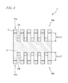
- FIG. 3 is a cross-sectional view for explaining a main part showing the concave-and-convex structure in the optical component according to another embodiment (Embodiment 2) of the present invention.
- FIG. 4 illustrates an optical component according to a still another embodiment (Embodiment 3) of the present invention.
- FIG. 5 illustrates a modification of the optical component according to Embodiment 3 of the present invention.
- FIG. 6 illustrates another modification of the optical component according to Embodiment 3 of the present invention.
- FIG. 7A is a plan view illustrating an optical component according to another embodiment (Embodiment 4) of the present invention.
- FIG. 7B illustrates a polarization state of laser light transmitted through the optical component according to Embodiment 4.
- FIG. 8 is a cross-sectional view for explaining a main section showing a concave-and-convex structure formed on the surface of the optical component as a modification of the optical component according to Embodiment 1 of the present invention.
- FIG. 9A to FIG. 9I illustrate a procedure for the manufacture method of the optical component according to Embodiment 3 of the present invention.
- FIG. 10A is a plan view illustrating a mask used in the manufacture method of the optical component according to Embodiment 3 of the present invention.
- FIG. 10B is an expanded view for explaining a main part illustrating a surface structure of the mask.
- FIG. 11 is a cross-sectional view for explaining a main section showing a concave-and-convex structure in an optical component used in Test Example 1.
- FIG. 12 illustrates a graph showing a result of the investigation in Test Example 1 of a relationship between the groove depth D in the optical component and the phase difference between the respective polarization components of the carbon dioxide laser light.
- FIG. 13 illustrates a graph showing a result of the investigation in Test Example 2 of a relationship between the groove depth D in the optical component and the transmittances of the respective polarization components of the carbon dioxide laser light.
- FIG. 14 illustrates a graph showing a result of the investigation in Example 1 of a relationship between the groove depth D in the optical component and the transmittances of the respective polarization components of the carbon dioxide laser light and the phase difference between the respective polarization components.
- FIG. 15 illustrates a graph showing a result of the investigation in Test Example 3 of a relationship between the inclination angle ⁇ of the optical component having thereon the concave-and-convex structure shown in FIG. 8 , the groove depth D, and the phase difference.
- optical component of the present invention will be described by an example of an optical element for converting a polarization state of carbon dioxide laser (transmission-type polarization filter).
- transmission-type polarization filter transmission-type polarization filter
- FIG. 1A is a perspective view illustrating an optical component according to one embodiment (Embodiment 1) of the present invention.
- FIG. 1B is a perspective view for explaining a main part showing a concave-and-convex structure in the optical component according to Embodiment 1.
- An optical component 1 shown in FIG. 1 is a transmission-type polarization filter that allows carbon dioxide laser light to transmit therethrough to thereby change the polarization state of the carbon dioxide laser light.
- This optical component 1 includes: a substrate body 2 that is a disc-shaped member having a concave-and-convex structure 10 on one surface thereof; and an antireflection film 3 layered on a surface of the concave-and-convex structure 10 (see FIG. 1B ).
- the substrate body 2 is a disc-shaped member made of ZnSe.
- the concave-and-convex structure 10 is formed in which projecting sections 11 and groove sections 12 are arranged at a spatial cycle equal to or lower than the wavelength of the carbon dioxide laser light.
- the substrate body 2 having the concave-and-convex structure 10 functions as a birefringent material that has different effective refractive indices depending on directions having or without having a spatial cycle.
- the difference in the effective refractive index as described above causes, for example, a difference in propagation speed between a polarization component incident perpendicularly to the direction of spatial cycle of the concave-and-convex structure 10 and a polarization component incident parallelly to the direction of the groove of the concave-and-convex structure 10 , thus resulting in a difference in phase delay between the polarization components.
- a phase difference can be caused in the carbon dioxide laser light incident to the optical component 1 .
- the substrate body 2 is made of ZnSe, and at least one surface of the member constituting the substrate body 2 has thereon the concave-and-convex structure 10 .
- the structural birefringence based on the concave-and-convex structure 10 can cause a phase difference in the transmitted carbon dioxide laser light, thus changing the polarization state of the carbon dioxide laser light.
- the substrate body 2 has a thickness usually in a range of about 1 to 10 mm at a part having the largest thickness (the projecting section 11 ).
- the diameter of the substrate body 2 can be appropriately set depending on a desired application, and can be set to 50 mm, for example. However, the diameter of the substrate body 2 is not particularly limited to this.
- the groove section 12 of the concave-and-convex structure 10 shown in FIG. 2 has a groove depth D that can be set depending on a wavelength and a desired phase difference of carbon dioxide laser light to be used.
- the difference in phase delay between polarization components is proportional to the depth D.
- the value of the depth D may be set depending on the desired phase difference.
- the depth D is preferably equal to or lower than 5.97 ⁇ m to 6.67 ⁇ m from the viewpoint of realizing the phase difference within an acceptable error of ⁇ 6 degrees.
- a pitch size (spatial cycle) P which is the sum of the width L 1 of the projecting section 11 and the width L 2 of the groove section 12 , is set to a short spatial cycle equal to or shorter than the wavelength of the carbon dioxide laser light to be used (9.3 to 10.6 ⁇ m). This can consequently suppress occurrence of diffracted light.
- the aspect ratio is preferably 2.76 to 2.96 from the viewpoint of realizing the phase difference within an acceptable error of ⁇ 6 degrees.
- the concave-and-convex structure 10 has a fill factor (the width L 1 of the projecting sections 11 /pitch size P) is preferably equal to or lower than 0.489 to 0.579 from the viewpoint of realizing the phase difference equal to or lower than 90 degrees ⁇ 6 degrees.
- the antireflection film 3 is a film made of material that has a lower refractive index than that of ZnSe.
- the material includes, for example, YF 3 , ThF 4 , YbF 3 , BaF 2 , HfF 4 , AlF 3 , LaF 3 , ZrF 4 or the like.
- the antireflection film 3 layered on the surface of the concave-and-convex structure 10 can suppress the reflection of the carbon dioxide laser light incident to the optical component 1 , thus improving the transmittance of the carbon dioxide laser light.
- the optical component 1 according to Embodiment 1 is preferably used for an application requiring a high output of carbon dioxide laser light.
- the optical component 1 according to Embodiment 1 can be manufactured by forming the concave-and-convex structure 10 on the surface of the member constituting the substrate body 2 to further layer the antireflection film 3 on the surface of the concave-and-convex structure 10 .
- the concave-and-convex structure 10 can be formed by subjecting the member constituting the substrate body 2 to, for example, an etching processing or the like.
- the antireflection film 3 can be layered on the surface of the concave-and-convex structure 10 by, for example, electron beam evaporation, sputtering, ion beam deposition or the like.
- FIG. 3 is a cross-sectional view for explaining a main part showing a concave-and-convex structure in an optical component according to another embodiment (Embodiment 2) of the present invention.
- the optical component 1 shown in FIG. 3 is different from the optical component 1 according to Embodiment 1 in that both surfaces of a substrate body 2 have the same concave-and-convex structures 10 a and 10 b.
- a difference in phase delay between polarization components of the carbon dioxide laser light is proportional to the depth that is the sum of groove depths of groove sections 12 a and 12 b of respective two concave-and-convex structures 10 a and 10 b.
- the concave-and-convex structure 10 that has a groove depth of 1 ⁇ 2 (d/2) as compared with the groove depth D (d) in the optical component 1 according to Embodiment 1.
- an etching processing or the like during the manufacture of the optical component 1 according to Embodiment 2 can be carried out in an easier manner than an etching processing or the like during the manufacture of the optical component 1 according to Embodiment 1.
- the optical component 1 according to Embodiment 2 can be manufactured more simply.
- the optical component 1 according to Embodiment 2 can be manufactured so that the angle ⁇ formed by the longitudinal direction axes of the groove sections 12 a and 12 b of the respective concave-and-convex structures 10 a and 10 b can be adjusted to form the concave-and-convex structures 10 a and 10 b in the substrate body 2 to thereby appropriately set a phase difference caused to occur in the carbon dioxide laser light (see FIG. 5 ).
- the optical component 1 according to Embodiment 2 is the same as the optical component 1 according to Embodiment 1 except for the points as described above.
- FIG. 4 illustrates an optical component according to still another embodiment (Embodiment 3) of the present invention.
- the optical component 1 of Embodiment 3 shown in FIG. 4 is different from the optical component 1 according to Embodiment 1 in that the optical component 1 of Embodiment 3 shown in FIG. 4 includes two substrate bodies 2 a and 2 b having the same concave-and-convex structures 10 a and 10 b , respectively.
- the optical component 1 according to Embodiment 3 includes: a member 1 a having a substrate body 2 a including the concave-and-convex structure 10 a ; and a member 1 b having a substrate body 2 b including the concave-and-convex structure 10 b .
- the substrate bodies 2 a and 2 b are disposed so that the surfaces thereof are spaced with a predetermined space therebetween and so that the respective concave-and-convex structures 10 a and 10 b are directed in the same direction.
- a difference in phase delay between polarization components of the carbon dioxide laser light is proportional to the depth that is the sum of the groove depths of the respective groove sections 12 a and 12 b of the two concave-and-convex structures 10 a and 10 b.
- the groove depths of the respective concave-and-convex structures 10 a and 10 b are 1 ⁇ 2 (d/2) of the groove depth D (d) in the optical component 1 according to Embodiment 1.
- a phase difference similar to that in the case of the optical component 1 according to Embodiment 1 can be caused to occur.
- the optical component 1 according to Embodiment 3 can easily be manufactured as the optical component according to Embodiment 2, and can cause a phase difference similar to that in the case of the optical component 1 according to Embodiment 1 to occur.
- the optical component 1 according to Embodiment 3 is composed of the members 1 a and 1 b .
- a relative angle ⁇ formed by longitudinal direction axes of the groove sections 12 a and 12 b of the respective members 1 a and 1 b can be appropriately adjusted to place both of the members 1 a and 1 b.
- the phase difference caused to occur in the carbon dioxide laser light can be adjusted easily, and the polarization state of the carbon dioxide laser light can be changed easily (see FIG. 5 ).
- FIG. 6 illustrates a modification of the optical component according to Embodiment 3 of the present invention.
- the optical component 1 according to this modification is different from the optical component 1 according to Embodiment 3 in that the substrate bodies 2 a and 2 b are disposed to have a predetermined space therebetween and that the concave-and-convex structures 10 a and 10 b are disposed so that the surfaces thereof are opposed to each other.
- optical component 1 according to this modification also provides the same effect as the optical component according to Embodiment 3.
- FIG. 7A is a plan view illustrating an optical component according to another embodiment (Embodiment 4) of the present invention.
- a substrate body 2 includes a disc-shaped member composed of one base member.
- the substrate body 2 is divided into a plurality of (or twelve) fan-shaped regions 21 a to 211 of which projecting sections 11 and groove sections 12 are formed in such a manner that directions thereof in the respective regions are different from one another.
- the plurality of fan-shaped regions 21 a to 211 are arranged so that directions forming the projecting sections 11 and the groove sections 12 continuously change among the fan-shaped regions adjacent to one another.
- the forming direction in the fan-shaped region 21 b is slightly inclined toward the left direction compared with the forming direction in the fan-shaped region 21 a in FIG. 7A .
- the forming direction in the fan-shaped region 21 c is further inclined toward the left direction compared with the formation direction of the fan-shaped region 21 b . In this manner, the inclination is increased sequentially.
- propagation speeds of the respective polarization components can be changed in the concave-and-convex structure 10 of the respective fan-shaped regions.
- phase difference can be continuously changed in the concave-and-convex structure 10 of the respective fan-shaped regions along the circumferential direction.
- polarization state of the carbon dioxide laser light can be converted from linear polarization to radial polarization (see FIG. 7B ).
- a stable processing surface can be formed during a processing of an object to be processed by carbon dioxide laser light.
- optical component according to Embodiment 4 is the same as the optical component 1 according to Embodiment 1 except for the points as described above.
- the disc-shaped member also may be the one that has the concave-and-convex structure 10 and that is arranged, by adhering a plurality of fan-shaped base members that have projecting sections 11 and groove sections 12 of the concave-and-convex structure 10 having different forming directions from each other so that the forming directions of the projecting sections 11 and the groove sections 12 continuously change along the circumferential direction of the disc-shaped member.
- a side wall of the projecting sections 11 of the concave-and-convex structure 10 may be inclined so that the side wall is inclined with respect to a direction perpendicular to a surface of the plate-like member constituting a substrate body 2 (see FIG. 8 ).
- the inclined side wall has an inclination angle ⁇ that is preferably equal to or lower than 18 degrees from the viewpoint of realizing a phase difference having an acceptable error equal to or lower than ⁇ 6 degrees.
- the pitch size P and the aspect ratio can be calculated by using the widths of the projecting sections 11 and the groove sections 12 at the depth of 1 ⁇ 2(d/2) of the groove depth D (d) in the substrate body 2 as the width L 1 of the projecting sections 11 and the width L 2 of the groove sections 12 .
- a side wall of the projecting section 11 of the concave-and-convex structure 10 may be the same inclined side wall as in this modification.
- the projecting section having the inclined side wall as described above can easily be formed by an etching processing or the like, thus simplifying the manufacture of the optical component.
- a film made of material having a higher refractive index than that of the material constituting the antireflection film 3 may be further layed on the surface of the antireflection film 3 .
- the film includes, for example, a film made of ZnSe or the like.
- FIG. 9A to FIG. 9I illustrate a procedure for the manufacture method of the substrate body used for an optical component according to Embodiment 4 of the present invention.
- FIG. 9A to FIG. 9I in order to simply explain the formation of the concave-and-convex structure, only a part of the concave-and-convex structure is shown in an exaggerated manner.
- a substrate 31 made of a transparent body such as ZnSe is coated with a photoresist that is photosensitive to light such as ultraviolet rays. Then, a photoresist layer 32 is formed on the surface of the substrate 31 , thereby obtaining a formed and fabricated material 33 ( FIG. 9A ).
- photoresist negative-type photoresist or positive-type photoresist can be used.
- the positive-type photoresist is preferred from the viewpoint of accurately forming a fan-shaped pattern.
- Such positive-type photoresist includes, for example, the one having a trade name of AZP4620 made by AZ Clariant or the like.
- the photoresist is coated, for example, by spin coating, spraying, dip coating or the like.
- the spin coating is preferred because the spin coating can provide an easy control of the thickness.
- a spin coater or the like can be used to coat the surface of the substrate 31 with the photoresist by a centrifugal force (e.g., rotation at 4000 rpm for 25 seconds).
- the thickness of the photoresist layer 32 is not particularly limited, and may be generally in a range from about 0.5 to 5 ⁇ m.
- the formed and fabricated material 33 after the resist coating is heated (or prebaked) by a heater 41 or the like to evaporate solvent components of the photoresist constituting the photoresist layer 32 to thereby solidify the photoresist layer 32 ( FIG. 9B ).
- a heating temperature can be appropriately set depending on a type of the solvent included in the photoresist or the like.
- the heating temperature is generally in a range from 80 to 120 degrees C.
- a heating time can be appropriately set depending on the heating temperature, the type of the solvent included in the photoresist, or the like.
- the heating time is generally 30 minutes to 1 hour when a bake furnace is used.
- the heating prebaking
- the heating is preferably carried out under a nitrogen atmosphere in order to avoid a rapid pressure increase due to ignition of the resist.
- a mask 34 is closely attached to the surface of the photoresist layer 32 of the formed and fabricated material 33 , and thereafter the photoresist layer 32 is exposed through the mask 34 ( FIG. 9C ).
- the mask 34 has a plane pattern having a plurality of fan-shaped regions (see FIG. 10A ).
- the arrows show the directions along which projecting sections and groove sections are formed.
- the mask 34 includes a masking section 34 a for shading exposure light and an opening section 34 b for transmitting exposure light (see FIG. 10B ).
- Exposure can be performed, for example, by ultraviolet rays. Such exposure can be performed, for example, by a simple contact exposure carried out by pressing the mask to the photoresist, a vacuum contact exposure carried out by pressing the mask and the photoresist to subsequently decompress the pressed part to thereby increase a degree of contact, or the like. An amount of light irradiated for the exposure can be appropriately set depending on the light to be used, the type or thickness of the photoresist, or the like.
- the formed and fabricated material 33 after the exposure is immersed in a developer 36 to perform a development, thereby obtaining a formed and fabricated material 35 ( FIG. 9D ).
- an alkali developer or the like can be used as a developer 36 .
- Such alkali developer includes, for example, a developer having a trade name of AZ DEVEROPPER made by AZ Clariant or the like.
- Development conditions can be appropriately set depending on the types of the photoresist and the developer 36 .
- the development conditions include, for example, conditions where the formed and fabricated material 35 is caused to oscillate for 240 seconds in the developer 36 retained at a temperature of 23 degrees C.
- the formed and fabricated material 35 after the development is cleaned to remove the developer left on the formed and fabricated material 35 ( FIG. 9E ).
- ultrapure water having a resistivity of 18.0M ⁇ or more can be caused to flow on the surface of the formed and fabricated material at a flow rate of 4 L/min for 2 minutes to thereby remove the developer left on the formed and fabricated material 35 .
- the formed and fabricated material 35 thus cleaned is heated (or post-baked) in a heater 41 to remove water left on the formed and fabricated material 35 ( FIG. 9F ).
- Heating conditions such as a heating temperature and a heating time may be ones similar to those for performing the prebaking.
- the non-exposed section 32 a accurately formed in the previous step functions as a mask.
- a pattern can be accurately formed in accordance with the plane pattern.
- the exposed part of the substrate 31 can be removed by dry etching, wet etching or the like. Among them, dry etching is preferred because dry etching can correctly remove the exposed part of the substrate 35 to correctly form a minute pattern.
- dry etching is performed, the exposed part in the substrate 31 is etched, whereas the non-exposed part of the substrate 31 superposed with the non-exposed section 32 a (projecting section 31 a ) is prevented from being etched because the non-exposed section 32 a functions as a mask. Thus, a pattern is formed on the surface of the substrate 31 .
- Dry etching is preferably RIE from the viewpoints of mass production and the apparatus cost.
- ICP-RIE inductive coupled plasma-reactive ion etching
- etching gas boron trichloride or the like can be used.
- Etching conditions such as etching gas flow rate, pressure, and etching time vary depending on a type of the etching gas and an etching depth of the exposed part, and thus cannot be determined commonly.
- the etching conditions may be, for example, the flow rate of 10 sccm, pressure of 3 Pa, and etching time of 50 minutes.
- the non-exposed section 32 a left on the substrate 31 is removed to thereby obtain the substrate body 2 having the concave-and-convex structure 10 ( FIG. 9H ).
- the non-exposed section 32 a can be removed, for example, by immersing the formed and fabricated material 37 after the etching in a solvent 38 for dissolving the photoresist constituting the non-exposed section 32 a .
- the dissolution of the photoresist is promoted by exposing the formed and fabricated material 37 immersed in the solvent 38 to ultrasonic waves.
- the solvent 38 for dissolving the photoresist can be appropriately selected depending on the type of the photoresist.
- the solvent 38 includes, for example, acetone or the like.
- an antireflection film 3 is formed on the concave-and-convex structure 10 of the substrate body 2 , to give the optical component 1 ( FIG. 9I ).
- the antireflection film 3 can be formed by layering the antireflection film 3 on the surface of the concave-and-convex structure 10 .
- the antireflection film 3 can be layered on the surface of the concave-and-convex structure 10 by electron beam evaporation, sputtering, or ion beam deposition, for example.
- a plate member made of ZnSe (diameter of 50 mm, thickness of 5 mm) was subjected to an etching processing so as to have various groove depths, to give a substrate body 2 in which the surface includes a concave-and-convex structure includes projecting sections 2 a and groove sections 2 b having a rectangular cross section ( FIG. 11 ) was obtained.
- the projecting sections as described above had a width of 1.6 ⁇ m, and the groove sections had a width of 2.4 ⁇ m.
- Carbon dioxide laser light having a wavelength of 10.6 ⁇ m was irradiated to the various substrate bodies 2 having different groove depths.
- FIG. 12 shows a relationship between the groove depth D of the optical components and the phase difference between the respective polarization components of the carbon dioxide laser light, in Test Example 1.
- the groove depth D is substantially proportional to the phase difference.
- the groove depth of 5.2 ⁇ m can provide the phase difference of 90 degrees between the respective polarization components (TE wave and TM wave) of the transmitted carbon dioxide laser light.
- designing the concave-and-convex structure in this manner can provide conversion of the polarization state of the carbon dioxide laser light from a linear polarization to a circular polarization.
- the respective substrate bodies 2 having various groove depths manufactured in Test Example 1 were used to investigate a relationship between the groove depth D and transmittances of the respective polarization components (TE wave and TM wave) of the carbon dioxide laser light having a wavelength of 10.6 ⁇ m.
- FIG. 13 shows a result of the investigation in Test Example 2 of a relationship between the groove depth D in an optical component and the transmittances of the respective polarization components of the carbon dioxide laser light.
- the respective polarization components (TE wave and TM wave) of the carbon dioxide laser light have different transmittances depending on a size of the groove depth D.
- the groove depth is 5.2 ⁇ m in the concave-and-convex structure in which the projecting section has a width of 1.6 ⁇ m and the groove section has a width of 2.4 ⁇ m
- the TE wave has a transmittance of 85%
- the TM wave has a transmittance of 96%.
- the laser processing of the object to be processed preferably obtains a transmittance of 96% or more in order to obtain a high output of carbon dioxide laser light.
- the section below will examine a means for obtaining a higher transmittance.
- a plate member made of ZnSe (diameter of 50 mm, thickness of 5 mm) was subjected to etching processings of varied conditions so as to have various groove depths, to give a substrate body in which the surface includes a concave-and-convex structure composed of a projecting section of width of 2.144 ⁇ m and a groove section of a width of 1.856 ⁇ m.
- a antireflection film made of YF 3 having a thickness of 1.77 ⁇ m was layered on the surface of the concave-and-convex structure of each substrate body, to give an optical component.
- the respective optical components thus obtained was used to investigate a relationship between a groove depth D and transmittances of the respective polarization components (TE wave and TM wave), and a relationship between a groove depth D and a phase difference between the respective polarization components of the carbon dioxide laser light having a wavelength of 10.6 ⁇ m.
- the result is shown in FIG. 14 .
- the respective polarization components (TE wave and TM wave) of the carbon dioxide laser light can have a transmittance of 96% or more, and that the phase difference between the respective polarization components can be adjusted to an arbitrary phase difference within a fixed range.
- the optical component shown in Table 1 below a high transmittance of 99% or more can be achieved for the respective polarization components of the carbon dioxide laser light, and the phase difference can be adjusted to 90 degrees, thereby converting the linear polarization to a circular polarization.
- an appropriate setting of the aspect ratio allows a phase difference between the respective polarization components of the carbon dioxide laser light to be a desired phase difference, thereby converting the polarization state of the carbon dioxide laser light, and achieves a high transmittance. Therefore, carbon dioxide laser light suitable for the laser processing of the object to be processed can be obtained.
- carbon dioxide laser light that is suitable for a laser processing of an object to be processed can be obtained by an optical component obtained by layering an antireflection film on a surface of a concave-and-convex structure of a substrate body made of ZnSe including the concave-and-convex structure.
- the concave-and-convex structure was composed of projecting sections having side walls of an inclination angle ⁇ of 0 degree, 10 degrees, or 20 degrees to a direction perpendicular to the surface of the plate-like member, and groove sections.
- the inclination angle ⁇ was 0 degree
- the projecting section had a width of 2.144 ⁇ m
- the groove section had a width of 1.856 ⁇ m.
- widths of the projecting section and the groove section were assumed to be the widths at a half depth of the groove depth (i.e., 1.6 ⁇ m and 2.4 ⁇ m, respectively).
- FIG. 15 shows a graph showing a result of a investigation in Test Example 3 of a relationship among the inclination angle ⁇ of the side wall of the projecting section of the optical component, the groove depth D, and the phase difference.
- the open circles show the result when the side wall of the projecting section has the inclination angle ⁇ of 0 degree.
- the closed triangles show the result when the side wall of the projecting section has the inclination angle ⁇ of 10 degrees.
- the closed squares show the result when the side wall of the projecting section has the inclination angle ⁇ of 20 degrees.
- a phase difference can be controlled as in the case where a projecting section does not have an inclined side wall.
Applications Claiming Priority (2)
| Application Number | Priority Date | Filing Date | Title |
|---|---|---|---|
| JP2010102840A JP5424154B2 (ja) | 2010-04-28 | 2010-04-28 | 光学部品 |
| JP2010-102840 | 2010-04-28 |
Publications (2)
| Publication Number | Publication Date |
|---|---|
| US20110268145A1 US20110268145A1 (en) | 2011-11-03 |
| US8854731B2 true US8854731B2 (en) | 2014-10-07 |
Family
ID=44260919
Family Applications (1)
| Application Number | Title | Priority Date | Filing Date |
|---|---|---|---|
| US13/090,989 Expired - Fee Related US8854731B2 (en) | 2010-04-28 | 2011-04-20 | Carbon dioxide laser light optical component |
Country Status (3)
| Country | Link |
|---|---|
| US (1) | US8854731B2 (ja) |
| EP (1) | EP2383589B1 (ja) |
| JP (1) | JP5424154B2 (ja) |
Families Citing this family (9)
| Publication number | Priority date | Publication date | Assignee | Title |
|---|---|---|---|---|
| JP5936574B2 (ja) * | 2012-07-06 | 2016-06-22 | 三菱電機株式会社 | 偏光位相差板およびレーザ加工機 |
| CN103529507B (zh) * | 2012-07-06 | 2016-05-25 | 三菱电机株式会社 | 偏振光相位差板以及激光加工机 |
| JP5945214B2 (ja) * | 2012-11-13 | 2016-07-05 | 住友電工ハードメタル株式会社 | 光学部品 |
| JP2015117147A (ja) * | 2013-12-18 | 2015-06-25 | 国立大学法人 東京大学 | ガラス部材の製造方法及びガラス部材 |
| US11231544B2 (en) | 2015-11-06 | 2022-01-25 | Magic Leap, Inc. | Metasurfaces for redirecting light and methods for fabricating |
| NZ747834A (en) | 2016-05-06 | 2023-06-30 | Magic Leap Inc | Metasurfaces with asymmetric gratings for redirecting light and methods for fabricating |
| CN110520763B (zh) | 2017-01-27 | 2021-10-26 | 奇跃公司 | 由具有不同取向的纳米梁的超表面形成的衍射光栅 |
| CA3051104A1 (en) | 2017-01-27 | 2018-08-02 | Magic Leap, Inc. | Antireflection coatings for metasurfaces |
| CN109711005B (zh) * | 2018-12-11 | 2021-06-08 | 浙江大学 | 一种无反射的波浪调控装置及设计方法 |
Citations (7)
| Publication number | Priority date | Publication date | Assignee | Title |
|---|---|---|---|---|
| US6030717A (en) * | 1997-01-23 | 2000-02-29 | Nikon Corporation | Multilayer antireflection coatings for grazing ultraviolet incident light |
| US20010053023A1 (en) * | 2000-05-22 | 2001-12-20 | Jasco Corporation | Wire grid type polarizer and method of manufacturing the same |
| US20020101663A1 (en) | 2001-01-29 | 2002-08-01 | Sumitomo Electric Industries, Ltd. | Diffractive optical element |
| US20020135847A1 (en) | 2001-03-22 | 2002-09-26 | Seiko Epson Corporation | Manufacturing method of microstructure, manufacturing method and manufacturing device of electronic device |
| JP2005010377A (ja) | 2003-06-18 | 2005-01-13 | Mankichi Yo | 光学位相差素子 |
| US6943941B2 (en) * | 2003-02-27 | 2005-09-13 | Asml Netherlands B.V. | Stationary and dynamic radial transverse electric polarizer for high numerical aperture systems |
| US8017923B2 (en) * | 2006-05-26 | 2011-09-13 | Nalux Co., Ltd | Infrared source and method of manufacturing the same |
Family Cites Families (9)
| Publication number | Priority date | Publication date | Assignee | Title |
|---|---|---|---|---|
| FR2413678A1 (fr) * | 1977-12-28 | 1979-07-27 | Marie G R P | Convertisseurs de mode d'une onde non confinante en une onde confinante dans l'infrarouge lointain |
| JP2850683B2 (ja) | 1992-12-18 | 1999-01-27 | 住友電気工業株式会社 | 円偏光ミラ− |
| JP3413067B2 (ja) * | 1997-07-29 | 2003-06-03 | キヤノン株式会社 | 投影光学系及びそれを用いた投影露光装置 |
| JP2004077806A (ja) * | 2002-08-19 | 2004-03-11 | Sanyo Electric Co Ltd | 位相板光学素子 |
| JP4814002B2 (ja) * | 2005-09-30 | 2011-11-09 | 株式会社リコー | 位相板の製造方法・光学素子および画像投射装置 |
| WO2007119838A1 (ja) * | 2006-04-11 | 2007-10-25 | Sumitomo Electric Hardmetal Corp. | Yagレーザー、ファイバレーザ用レンズおよびレーザ加工装置 |
| WO2007142179A1 (ja) * | 2006-06-07 | 2007-12-13 | Konica Minolta Holdings, Inc. | 四分の一波長板及び光ピックアップ装置 |
| JP5526474B2 (ja) * | 2007-03-26 | 2014-06-18 | 株式会社リコー | 微小構造体の形成方法 |
| JP2008287747A (ja) * | 2007-05-15 | 2008-11-27 | Konica Minolta Opto Inc | λ/4波長板及び光ピックアップ装置 |
-
2010
- 2010-04-28 JP JP2010102840A patent/JP5424154B2/ja not_active Expired - Fee Related
-
2011
- 2011-04-20 US US13/090,989 patent/US8854731B2/en not_active Expired - Fee Related
- 2011-04-26 EP EP11163649.4A patent/EP2383589B1/en not_active Not-in-force
Patent Citations (7)
| Publication number | Priority date | Publication date | Assignee | Title |
|---|---|---|---|---|
| US6030717A (en) * | 1997-01-23 | 2000-02-29 | Nikon Corporation | Multilayer antireflection coatings for grazing ultraviolet incident light |
| US20010053023A1 (en) * | 2000-05-22 | 2001-12-20 | Jasco Corporation | Wire grid type polarizer and method of manufacturing the same |
| US20020101663A1 (en) | 2001-01-29 | 2002-08-01 | Sumitomo Electric Industries, Ltd. | Diffractive optical element |
| US20020135847A1 (en) | 2001-03-22 | 2002-09-26 | Seiko Epson Corporation | Manufacturing method of microstructure, manufacturing method and manufacturing device of electronic device |
| US6943941B2 (en) * | 2003-02-27 | 2005-09-13 | Asml Netherlands B.V. | Stationary and dynamic radial transverse electric polarizer for high numerical aperture systems |
| JP2005010377A (ja) | 2003-06-18 | 2005-01-13 | Mankichi Yo | 光学位相差素子 |
| US8017923B2 (en) * | 2006-05-26 | 2011-09-13 | Nalux Co., Ltd | Infrared source and method of manufacturing the same |
Non-Patent Citations (1)
| Title |
|---|
| Guoguo Kang, et al., Achromatic phase retarder applied to MWIR and LWIR dual-band, Optics Express, vol. 18, No. 2, Jan. 14, 2010 pp. 1695-1703. |
Also Published As
| Publication number | Publication date |
|---|---|
| JP5424154B2 (ja) | 2014-02-26 |
| EP2383589A1 (en) | 2011-11-02 |
| EP2383589B1 (en) | 2013-09-18 |
| JP2011232551A (ja) | 2011-11-17 |
| US20110268145A1 (en) | 2011-11-03 |
Similar Documents
| Publication | Publication Date | Title |
|---|---|---|
| US8854731B2 (en) | Carbon dioxide laser light optical component | |
| US4013465A (en) | Reducing the reflectance of surfaces to radiation | |
| US4402571A (en) | Method for producing a surface relief pattern | |
| EP0271002A2 (en) | Transmittance modulation photomask, process for producing the same and process for producing diffraction grating | |
| US20030223118A1 (en) | Optical component and method of manufacturing same | |
| EP0323238A2 (en) | Diffraction grating and manufacturing method thereof | |
| JP2010169722A (ja) | 光学素子の製造方法及び光学素子 | |
| JPS59124306A (ja) | 光集積回路素子およびその作製方法 | |
| JP2004012856A (ja) | 光学素子、光学素子の成形型および光学素子の製造方法 | |
| US20090267245A1 (en) | Transmission Type Optical Element | |
| JP2006038928A (ja) | 無反射周期構造体及びその製造方法 | |
| US20060216478A1 (en) | Grating, negative and replica gratings of the grating, and method of manufacturing the same | |
| JPH0653122A (ja) | レジストパタ−ンの形成方法 | |
| JPS6252506A (ja) | グレ−テイング作製方法 | |
| JPH0815510A (ja) | バイナリーオプティクス及びその製造方法 | |
| US20030124313A1 (en) | Grating, negative and replica gratings of the grating, and method of manufacturing the same | |
| US7407737B2 (en) | Method for the production of photoresist structures | |
| JP2000056135A (ja) | 全反射(tir)ホログラフィ装置、その方法及び使用される光学アセンブリ | |
| JPH041703A (ja) | 位相シフト型回折格子の製造方法 | |
| JPS6127505A (ja) | プレ−ズ光学素子の製造方法 | |
| JPH03242648A (ja) | ホトマスクの製造方法 | |
| JPS6271907A (ja) | グレ−テイング光デバイス | |
| JPH0456284B2 (ja) | ||
| JPH0812287B2 (ja) | グレーティング作製方法 | |
| WO2024014272A1 (ja) | メタレンズ、メタレンズの製造方法、電子機器、メタレンズの設計方法 |
Legal Events
| Date | Code | Title | Description |
|---|---|---|---|
| AS | Assignment |
Owner name: OSAKA PREFECTURE UNIVERSITY PUBLIC CORPORATION, JA Free format text: ASSIGNMENT OF ASSIGNORS INTEREST;ASSIGNORS:KIKUTA, HISAO;KURISU, KENICHI;EBATA, KEIJI;SIGNING DATES FROM 20110419 TO 20110422;REEL/FRAME:026402/0833 Owner name: SUMITOMO ELECTRIC INDUSTRIES, LTD., JAPAN Free format text: ASSIGNMENT OF ASSIGNORS INTEREST;ASSIGNORS:KIKUTA, HISAO;KURISU, KENICHI;EBATA, KEIJI;SIGNING DATES FROM 20110419 TO 20110422;REEL/FRAME:026402/0833 Owner name: SUMITOMO ELECTRIC HARDMETAL CORP., JAPAN Free format text: ASSIGNMENT OF ASSIGNORS INTEREST;ASSIGNORS:KIKUTA, HISAO;KURISU, KENICHI;EBATA, KEIJI;SIGNING DATES FROM 20110419 TO 20110422;REEL/FRAME:026402/0833 |
|
| FEPP | Fee payment procedure |
Free format text: PAYOR NUMBER ASSIGNED (ORIGINAL EVENT CODE: ASPN); ENTITY STATUS OF PATENT OWNER: LARGE ENTITY |
|
| FEPP | Fee payment procedure |
Free format text: MAINTENANCE FEE REMINDER MAILED (ORIGINAL EVENT CODE: REM.) |
|
| LAPS | Lapse for failure to pay maintenance fees |
Free format text: PATENT EXPIRED FOR FAILURE TO PAY MAINTENANCE FEES (ORIGINAL EVENT CODE: EXP.); ENTITY STATUS OF PATENT OWNER: LARGE ENTITY |
|
| STCH | Information on status: patent discontinuation |
Free format text: PATENT EXPIRED DUE TO NONPAYMENT OF MAINTENANCE FEES UNDER 37 CFR 1.362 |
|
| FP | Lapsed due to failure to pay maintenance fee |
Effective date: 20181007 |