US8854036B2 - Current detecting apparatus - Google Patents
Current detecting apparatus Download PDFInfo
- Publication number
- US8854036B2 US8854036B2 US13/655,503 US201213655503A US8854036B2 US 8854036 B2 US8854036 B2 US 8854036B2 US 201213655503 A US201213655503 A US 201213655503A US 8854036 B2 US8854036 B2 US 8854036B2
- Authority
- US
- United States
- Prior art keywords
- circuit board
- magnetic core
- connector
- container member
- detecting apparatus
- Prior art date
- Legal status (The legal status is an assumption and is not a legal conclusion. Google has not performed a legal analysis and makes no representation as to the accuracy of the status listed.)
- Active, expires
Links
Images


Classifications
-
- G—PHYSICS
- G01—MEASURING; TESTING
- G01R—MEASURING ELECTRIC VARIABLES; MEASURING MAGNETIC VARIABLES
- G01R33/00—Arrangements or instruments for measuring magnetic variables
- G01R33/02—Measuring direction or magnitude of magnetic fields or magnetic flux
- G01R33/06—Measuring direction or magnitude of magnetic fields or magnetic flux using galvano-magnetic devices
- G01R33/09—Magnetoresistive devices
-
- G—PHYSICS
- G01—MEASURING; TESTING
- G01R—MEASURING ELECTRIC VARIABLES; MEASURING MAGNETIC VARIABLES
- G01R15/00—Details of measuring arrangements of the types provided for in groups G01R17/00 - G01R29/00, G01R33/00 - G01R33/26 or G01R35/00
- G01R15/14—Adaptations providing voltage or current isolation, e.g. for high-voltage or high-current networks
- G01R15/20—Adaptations providing voltage or current isolation, e.g. for high-voltage or high-current networks using galvano-magnetic devices, e.g. Hall-effect devices, i.e. measuring a magnetic field via the interaction between a current and a magnetic field, e.g. magneto resistive or Hall effect devices
- G01R15/202—Adaptations providing voltage or current isolation, e.g. for high-voltage or high-current networks using galvano-magnetic devices, e.g. Hall-effect devices, i.e. measuring a magnetic field via the interaction between a current and a magnetic field, e.g. magneto resistive or Hall effect devices using Hall-effect devices
-
- G—PHYSICS
- G01—MEASURING; TESTING
- G01R—MEASURING ELECTRIC VARIABLES; MEASURING MAGNETIC VARIABLES
- G01R15/00—Details of measuring arrangements of the types provided for in groups G01R17/00 - G01R29/00, G01R33/00 - G01R33/26 or G01R35/00
- G01R15/14—Adaptations providing voltage or current isolation, e.g. for high-voltage or high-current networks
- G01R15/20—Adaptations providing voltage or current isolation, e.g. for high-voltage or high-current networks using galvano-magnetic devices, e.g. Hall-effect devices, i.e. measuring a magnetic field via the interaction between a current and a magnetic field, e.g. magneto resistive or Hall effect devices
- G01R15/207—Constructional details independent of the type of device used
Definitions
- the current detecting apparatus of the magnetic proportion system or of the magnetic balance system includes, as described in JP2004-A-101384, for example, a magnetic core and a magnetoelectric device (magnetic induction device).
- the magnetic core is a substantially ring-shaped magnetic body having ends facing each other via a gap portion therebetween and formed continuously so as to surround the periphery of a hollow portion where the bus bar penetrates.
- the hollow portion of the magnetic body is a space where the detected current passes through.
- a magnetism detecting portion of the magnetoelectric device is arranged at the gap portion of the magnetic core, and a lead terminal extending from the magnetism detecting portion is secured to a circuit board by soldering together with the lead terminal of a connector connected to a cable with a connector for transmitting a signal and other electronic components.
- the circuit board thereof is fixed to screw seats provided on parts of the housing with screws.
- the circuit board is susceptible to a deflection due to a change in environmental temperature.
- the deflection (warp) of the circuit board may cause a displacement of a positional relationship between the magnetoelectric device and the magnetic core mounted on the circuit board and hence may cause deterioration of current detection accuracy.
- a general-purpose connector including the body portion and the lead terminal integrated with high degree of dimensional accuracy in advance (commercially available connector) is employed, and such a general-purpose connector is mounted on the circuit board.
- the circuit board is susceptible to a deflection because the circuit board is formed to be relatively large and a force is applied to the circuit board via the connector at the time of connection and disconnection of the cable with a connector with respect to the connector. Therefore, when the general-purpose connector is mounted on the circuit board, deterioration of the current detection accuracy due to the displacement of the positional relationship between the magnetoelectric device and the magnetic core becomes apparent.
- JP-A-2004-101384 there is no description about a detailed structure for reducing the deflection of the circuit board on which the magnetoelectric device is mounted in the current detecting apparatus.
- the lid-side substrate holding portion is a lid-side substrate holding portion formed so as to project from the lid member, and having a top portion coming into contact at least with second surfaces of the second portion and the third portion of the circuit board, and configured to hold the circuit board tightly with the container-side substrate holding portion.
- the current detecting apparatus may further include a connector fixed to the circuit board and electrically connected to the magnetoelectric device.
- the housing may further include a connector positioning portion formed on the container member and configured to hold the position of the connector in dimensions of three directions.
- the circuit board on which the magnetoelectric device is mounted is fixed to the substrate fixing portion of the housing at the first portion, and is held tightly between the container-side substrate holding portion and the lid-side substrate holding portion of the housing at the second portion and the third portion. Therefore, the first portion, the second portion, and the third portion of the circuit board can be set within a very small range, so that the area surrounded by the three portions of the circuit board is hardly deflected.
- the area surrounded by the first to third portions of the circuit board is referred to as a “surrounded area”.
- the magnetoelectric device Since the magnetoelectric device is mounted in the surrounded area on the circuit board, the displacement of the magnetoelectric device caused by the deflection (warp) of the circuit board hardly occurs. Therefore, according to exemplary embodiments, deterioration of the current detection accuracy caused by a displacement of a positional relationship between a magnetoelectric device and a magnetic core mounted on the circuit board may be reduced.
- the substrate rotation restricting portion restricts the circuit board, fixed at one point by the substrate fixing portion, from rotating. Consequently, the positional displacement of the magnetoelectric device and the deterioration of the current detection accuracy caused by the rotation of the circuit board are also reduced. In comparison with a case where the circuit board is fixed at a plurality of points by fastening screws or the like, the number of steps of fixing work of the circuit board is reduced.
- positioning of the connector fixed to the circuit board is achieved by the housing. Therefore, the external force applied to the connector dispersedly acts on the connector positioning portion of the housing and the circuit board, and the influence of the external force applied to the connector on the positional displacement of the circuit board and the magnetoelectric device is alleviated. Consequently, the positional displacement of the magnetoelectric device and the deterioration of the current detection accuracy caused by the external force applied to the connector are reduced more reliably.
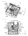
- FIG. 6 is a front view of a portion configured to support a magnetic core in the container member.
- FIG. 9 is a front view of the connector positioning portion configured to support the connector.
- a transmission channel 30 such as a bus bar through which electric current to be detected flows is arranged so as to penetrate through the hollow portion 11 of the magnetic core 10 .
- the transmission channel 30 is illustrated by an imaginary line (double-dashed chain line).
- a state in which the detection center of the magnetism detecting portion 21 is located at a center point of the gap portion 12 of the magnetic core 10 , and the reference straight line of the magnetism detecting portion 21 overlaps with a straight line connecting centers of projecting surfaces of the facing both end surfaces 13 of the magnetic core 10 is an ideal state of arrangement of the magnetism detecting portion 21 .
- the circuit board 50 is formed with two first through holes 51 which allow penetration of two of the first screws 71 respectively and the one second through hole 52 which allows penetration of the one second screw 72 .
- the first screws 71 are screws for fixing a body portion 61 of the connector 60 to the circuit board 50 .
- the second screw 72 is a screw for fixing the circuit board 50 to the container member 41 of the insulating housing 40 .
- a plurality of the lead terminals 62 of the connector 60 are inserted into connector mounting holes 54 formed on the circuit board 50 , and are secured to the wiring pattern of the circuit board 50 by soldering.
- the container member 41 is formed into a box-shape having an opening and the lid member 42 closes the opening of the container member 41 by being assembled to the container member 41 .
- the container member 41 and the lid member 42 are formed with a current pass hole 401 as a through hole which allows insertion of the transmission channel 30 .
- the inner frame portion 421 of the lid member 42 is a portion formed to be specially thin and tall among the projections formed in the insulating housing 40 . Therefore, when the lid member 42 is molded by injection molding and then cooled down, the inner frame portion 421 is liable to be deformed into an obliquely inclined shape from its original shape.
- a core positioning portion 43 , an element positioning portion 44 , and a connector positioning portion 45 configured to support the magnetic core 10 , the Hall element 20 , and the body portion 61 of the connector 60 are formed respectively at predetermined positions inside the container member 41 . Furthermore, a substrate fixing portion 46 to which the circuit board 50 is fixed at one point thereof is also formed inside the container member 41 . A supporting structure of the respective components will be described.
- FIG. 7 is a lateral cross-section of the connector positioning portion 45 configured to support the connector 60 , and is a cross-sectional view taken along a II-II plane illustrated in FIG. 5 .
- FIG. 8 is a back view of the container member 41 configured to support the connector 60 .
- FIG. 9 is a front view of the connector positioning portion 45 configured to support the connector 60 .
- FIG. 9 is an enlarged view of a portion surrounded by a frame border III in FIG. 5 .
- the second connector positioning portion 452 includes a plurality of protrusion portions 4520 formed so as to protrude from both sides of the fourth side surface 614 of the body portion 61 of the connector 60 .
- four of the protrusion portions 4520 are formed so as to protrude from the pair of first connector positioning portions 451 , respectively.
- the four protrusion portions 4520 are formed at positions which form corners of a rectangle when viewed from the first direction.
- the guide rib 48 restricts the circuit board 50 fixed at one point by the substrate fixing portion 46 from rotating. Consequently, the possibility of positional displacement of the Hall element 20 and the possibility of deterioration of the current detection accuracy caused by the rotation of the circuit board 50 are reduced. Since the circuit board 50 is fixed by the second screw 72 only at one point, the number of steps in the fixing work of the circuit board 50 is reduced in comparison with a case of being secured at a plurality of points with screws.
- the container member 41 which is an integrally molded member formed of a resin material is formed with high degree of dimensional accuracy. Therefore, positioning of the lead terminals 22 of the Hall element 20 and the lead terminals 62 of the connector 60 is achieved with high degree of accuracy by the container member 41 .
- the Hall element 20 , the connector 60 , and the circuit board 50 on which the Hall element 20 and the connector 60 are mounted may be fixed firmly with high degree of positional accuracy while employing the general-purpose connector 60 in the simple assembling process. Consequently, the mounting error of the components is reduced, and variations in detection accuracy of the current detecting apparatus 1 may be reduced.
- the lid-side substrate holding portion 423 may be formed of two projections facing the two core inner-edge positioning portions 43 a .
- the one core inner-edge positioning portion 43 a may be formed to have a width coming into contact with both of the second portion 502 and the third portion 503 which surround the mounting portion of the Hall element 20 from three sides in cooperation with the first portion 501 of the circuit board 50 .
Landscapes
- Physics & Mathematics (AREA)
- General Physics & Mathematics (AREA)
- Condensed Matter Physics & Semiconductors (AREA)
- Measuring Instrument Details And Bridges, And Automatic Balancing Devices (AREA)
Applications Claiming Priority (2)
| Application Number | Priority Date | Filing Date | Title |
|---|---|---|---|
| JP2011-281436 | 2011-12-22 | ||
| JP2011281436A JP5817508B2 (ja) | 2011-12-22 | 2011-12-22 | 電流検出装置 |
Publications (2)
| Publication Number | Publication Date |
|---|---|
| US20130162246A1 US20130162246A1 (en) | 2013-06-27 |
| US8854036B2 true US8854036B2 (en) | 2014-10-07 |
Family
ID=48653878
Family Applications (1)
| Application Number | Title | Priority Date | Filing Date |
|---|---|---|---|
| US13/655,503 Active 2032-11-16 US8854036B2 (en) | 2011-12-22 | 2012-10-19 | Current detecting apparatus |
Country Status (2)
| Country | Link |
|---|---|
| US (1) | US8854036B2 (ja) |
| JP (1) | JP5817508B2 (ja) |
Cited By (2)
| Publication number | Priority date | Publication date | Assignee | Title |
|---|---|---|---|---|
| EP3761045A1 (en) * | 2019-07-01 | 2021-01-06 | Tamura Corporation | Electronic device and current sensor |
| US20220178972A1 (en) * | 2019-03-15 | 2022-06-09 | Tdk Corporation | Current sensor |
Families Citing this family (10)
| Publication number | Priority date | Publication date | Assignee | Title |
|---|---|---|---|---|
| JP5948889B2 (ja) * | 2012-01-20 | 2016-07-06 | 株式会社オートネットワーク技術研究所 | 電流検出装置 |
| JP6030866B2 (ja) * | 2012-06-14 | 2016-11-24 | 矢崎総業株式会社 | 電流センサ |
| JP5800207B2 (ja) * | 2013-05-10 | 2015-10-28 | 株式会社デンソー | 回転位置検出装置 |
| TWI553317B (zh) * | 2014-05-06 | 2016-10-11 | Molex Inc | Modules with integrated sensors |
| EP3159705A1 (en) * | 2015-10-23 | 2017-04-26 | LEM Intellectual Property SA | Current transducer with integrated primary conductor |
| EP3306325B1 (en) * | 2016-10-05 | 2021-07-21 | Fico Triad, S.A. | A current measuring device |
| JP6932561B2 (ja) * | 2017-06-15 | 2021-09-08 | キヤノン電子株式会社 | 3軸磁気検出装置および人工衛星 |
| EP3726228B1 (en) * | 2017-12-13 | 2023-06-07 | Alps Alpine Co., Ltd. | Current sensor |
| KR102258813B1 (ko) * | 2018-11-20 | 2021-05-31 | 주식회사 엘지에너지솔루션 | 복합형 전류 측정장치 |
| JP7109407B2 (ja) * | 2019-07-01 | 2022-07-29 | 株式会社タムラ製作所 | 電流検出器 |
Citations (4)
| Publication number | Priority date | Publication date | Assignee | Title |
|---|---|---|---|---|
| US4972140A (en) | 1988-06-14 | 1990-11-20 | Stanley Electric Co., Ltd. | Current detection device and core for detection of magnetic flux |
| JPH0786769A (ja) * | 1993-07-19 | 1995-03-31 | Stanley Electric Co Ltd | 電気装置用の箱体 |
| JPH07260829A (ja) * | 1994-03-25 | 1995-10-13 | Tokin Corp | 電流検出器 |
| JP2004101384A (ja) | 2002-09-10 | 2004-04-02 | Yazaki Corp | 電流検出装置 |
Family Cites Families (6)
| Publication number | Priority date | Publication date | Assignee | Title |
|---|---|---|---|---|
| JPH0517820Y2 (ja) * | 1987-09-08 | 1993-05-12 | ||
| JPH04282461A (ja) * | 1991-03-12 | 1992-10-07 | Mitsubishi Electric Corp | 電流検出器 |
| JP2504746Y2 (ja) * | 1993-05-21 | 1996-07-10 | スタンレー電気株式会社 | 電流検出装置 |
| JPH10253666A (ja) * | 1997-03-14 | 1998-09-25 | Stanley Electric Co Ltd | 電流検出装置 |
| JP2002296305A (ja) * | 2001-04-02 | 2002-10-09 | Jeco Co Ltd | 電流センサのコア |
| JP2005308526A (ja) * | 2004-04-21 | 2005-11-04 | Denso Corp | 電流センサ |
-
2011
- 2011-12-22 JP JP2011281436A patent/JP5817508B2/ja not_active Expired - Fee Related
-
2012
- 2012-10-19 US US13/655,503 patent/US8854036B2/en active Active
Patent Citations (4)
| Publication number | Priority date | Publication date | Assignee | Title |
|---|---|---|---|---|
| US4972140A (en) | 1988-06-14 | 1990-11-20 | Stanley Electric Co., Ltd. | Current detection device and core for detection of magnetic flux |
| JPH0786769A (ja) * | 1993-07-19 | 1995-03-31 | Stanley Electric Co Ltd | 電気装置用の箱体 |
| JPH07260829A (ja) * | 1994-03-25 | 1995-10-13 | Tokin Corp | 電流検出器 |
| JP2004101384A (ja) | 2002-09-10 | 2004-04-02 | Yazaki Corp | 電流検出装置 |
Non-Patent Citations (3)
| Title |
|---|
| Feb. 27, 2014 Non-Final Rejection issued in U.S. Appl. No. 13/647,946. |
| Machine English translation of Japanese Patent Application Publication to Inventor Minoru Noda. JP 1995-260829 A, Oct. 13, 1995. Translation of pp. 2-4 created on Feb. 11, 2014. * |
| Machine English translation of Japanese Patent Application Publication to Inventor S Kajiya et. al. JP 1995-086769 A, Mar. 31, 1995. Translation of pp. 2-5 created on Feb. 21, 2014. * |
Cited By (2)
| Publication number | Priority date | Publication date | Assignee | Title |
|---|---|---|---|---|
| US20220178972A1 (en) * | 2019-03-15 | 2022-06-09 | Tdk Corporation | Current sensor |
| EP3761045A1 (en) * | 2019-07-01 | 2021-01-06 | Tamura Corporation | Electronic device and current sensor |
Also Published As
| Publication number | Publication date |
|---|---|
| JP5817508B2 (ja) | 2015-11-18 |
| JP2013130518A (ja) | 2013-07-04 |
| US20130162246A1 (en) | 2013-06-27 |
Similar Documents
| Publication | Publication Date | Title |
|---|---|---|
| US8854036B2 (en) | Current detecting apparatus | |
| US8947083B2 (en) | Current detecting apparatus | |
| US9086440B2 (en) | Current sensor | |
| US8237435B2 (en) | Assembling structure of current detection apparatus | |
| US7583072B2 (en) | Current sensor for measuring current flowing through bus bar | |
| JP5403792B2 (ja) | 電流検出装置の組付け構造 | |
| US20140225593A1 (en) | Current detection device | |
| US9255976B2 (en) | Current detection device | |
| JP5673085B2 (ja) | 電流検出装置 | |
| WO2019117169A1 (ja) | 電流センサ | |
| EP3244216B1 (en) | Current detector | |
| CN103134973A (zh) | 电流检测装置 | |
| JP6064117B2 (ja) | 電流センサ | |
| JP2013140089A (ja) | 電流検出装置 | |
| JP6890679B2 (ja) | 電流センサ | |
| JP5683511B2 (ja) | 電流センサ | |
| JP7472280B2 (ja) | 電流センサ | |
| JP5948889B2 (ja) | 電流検出装置 | |
| WO2013027424A1 (ja) | 電流検出装置 | |
| JP2015145839A (ja) | 電流検出装置 | |
| JP2013142579A (ja) | 電流検出装置 | |
| JP2015083950A (ja) | 電流検出装置 | |
| JP2013101014A (ja) | 電流検出装置 | |
| JP2013015364A (ja) | 電流検出装置 | |
| JP2013015365A (ja) | 電流検出装置 |
Legal Events
| Date | Code | Title | Description |
|---|---|---|---|
| AS | Assignment |
Owner name: SUMITOMO WIRING SYSTEMS, LTD., JAPAN Free format text: ASSIGNMENT OF ASSIGNORS INTEREST;ASSIGNORS:NAKAJIMA, HIROKATSU;CHAEN, SATORU;REEL/FRAME:029363/0346 Effective date: 20121012 |
|
| STCF | Information on status: patent grant |
Free format text: PATENTED CASE |
|
| MAFP | Maintenance fee payment |
Free format text: PAYMENT OF MAINTENANCE FEE, 4TH YEAR, LARGE ENTITY (ORIGINAL EVENT CODE: M1551) Year of fee payment: 4 |
|
| MAFP | Maintenance fee payment |
Free format text: PAYMENT OF MAINTENANCE FEE, 8TH YEAR, LARGE ENTITY (ORIGINAL EVENT CODE: M1552); ENTITY STATUS OF PATENT OWNER: LARGE ENTITY Year of fee payment: 8 |