US7170917B2 - Surface-emitting semiconductor laser - Google Patents
Surface-emitting semiconductor laser Download PDFInfo
- Publication number
- US7170917B2 US7170917B2 US10/468,183 US46818304A US7170917B2 US 7170917 B2 US7170917 B2 US 7170917B2 US 46818304 A US46818304 A US 46818304A US 7170917 B2 US7170917 B2 US 7170917B2
- Authority
- US
- United States
- Prior art keywords
- layer
- semiconductor laser
- diffusion barrier
- dielectric mirror
- applying
- Prior art date
- Legal status (The legal status is an assumption and is not a legal conclusion. Google has not performed a legal analysis and makes no representation as to the accuracy of the status listed.)
- Expired - Lifetime, expires
Links
Images


Classifications
-
- H—ELECTRICITY
- H01—ELECTRIC ELEMENTS
- H01S—DEVICES USING THE PROCESS OF LIGHT AMPLIFICATION BY STIMULATED EMISSION OF RADIATION [LASER] TO AMPLIFY OR GENERATE LIGHT; DEVICES USING STIMULATED EMISSION OF ELECTROMAGNETIC RADIATION IN WAVE RANGES OTHER THAN OPTICAL
- H01S5/00—Semiconductor lasers
- H01S5/10—Construction or shape of the optical resonator, e.g. extended or external cavity, coupled cavities, bent-guide, varying width, thickness or composition of the active region
- H01S5/18—Surface-emitting [SE] lasers, e.g. having both horizontal and vertical cavities
- H01S5/183—Surface-emitting [SE] lasers, e.g. having both horizontal and vertical cavities having only vertical cavities, e.g. vertical cavity surface-emitting lasers [VCSEL]
- H01S5/18361—Structure of the reflectors, e.g. hybrid mirrors
- H01S5/18369—Structure of the reflectors, e.g. hybrid mirrors based on dielectric materials
-
- H—ELECTRICITY
- H01—ELECTRIC ELEMENTS
- H01S—DEVICES USING THE PROCESS OF LIGHT AMPLIFICATION BY STIMULATED EMISSION OF RADIATION [LASER] TO AMPLIFY OR GENERATE LIGHT; DEVICES USING STIMULATED EMISSION OF ELECTROMAGNETIC RADIATION IN WAVE RANGES OTHER THAN OPTICAL
- H01S5/00—Semiconductor lasers
- H01S5/04—Processes or apparatus for excitation, e.g. pumping, e.g. by electron beams
- H01S5/042—Electrical excitation ; Circuits therefor
- H01S5/0425—Electrodes, e.g. characterised by the structure
- H01S5/04252—Electrodes, e.g. characterised by the structure characterised by the material
-
- H—ELECTRICITY
- H01—ELECTRIC ELEMENTS
- H01S—DEVICES USING THE PROCESS OF LIGHT AMPLIFICATION BY STIMULATED EMISSION OF RADIATION [LASER] TO AMPLIFY OR GENERATE LIGHT; DEVICES USING STIMULATED EMISSION OF ELECTROMAGNETIC RADIATION IN WAVE RANGES OTHER THAN OPTICAL
- H01S5/00—Semiconductor lasers
- H01S5/02—Structural details or components not essential to laser action
- H01S5/0206—Substrates, e.g. growth, shape, material, removal or bonding
- H01S5/0217—Removal of the substrate
-
- H—ELECTRICITY
- H01—ELECTRIC ELEMENTS
- H01S—DEVICES USING THE PROCESS OF LIGHT AMPLIFICATION BY STIMULATED EMISSION OF RADIATION [LASER] TO AMPLIFY OR GENERATE LIGHT; DEVICES USING STIMULATED EMISSION OF ELECTROMAGNETIC RADIATION IN WAVE RANGES OTHER THAN OPTICAL
- H01S5/00—Semiconductor lasers
- H01S5/02—Structural details or components not essential to laser action
- H01S5/024—Arrangements for thermal management
- H01S5/02476—Heat spreaders, i.e. improving heat flow between laser chip and heat dissipating elements
-
- H—ELECTRICITY
- H01—ELECTRIC ELEMENTS
- H01S—DEVICES USING THE PROCESS OF LIGHT AMPLIFICATION BY STIMULATED EMISSION OF RADIATION [LASER] TO AMPLIFY OR GENERATE LIGHT; DEVICES USING STIMULATED EMISSION OF ELECTROMAGNETIC RADIATION IN WAVE RANGES OTHER THAN OPTICAL
- H01S5/00—Semiconductor lasers
- H01S5/04—Processes or apparatus for excitation, e.g. pumping, e.g. by electron beams
- H01S5/042—Electrical excitation ; Circuits therefor
- H01S5/0421—Electrical excitation ; Circuits therefor characterised by the semiconducting contacting layers
-
- H—ELECTRICITY
- H01—ELECTRIC ELEMENTS
- H01S—DEVICES USING THE PROCESS OF LIGHT AMPLIFICATION BY STIMULATED EMISSION OF RADIATION [LASER] TO AMPLIFY OR GENERATE LIGHT; DEVICES USING STIMULATED EMISSION OF ELECTROMAGNETIC RADIATION IN WAVE RANGES OTHER THAN OPTICAL
- H01S5/00—Semiconductor lasers
- H01S5/04—Processes or apparatus for excitation, e.g. pumping, e.g. by electron beams
- H01S5/042—Electrical excitation ; Circuits therefor
- H01S5/0425—Electrodes, e.g. characterised by the structure
- H01S5/04252—Electrodes, e.g. characterised by the structure characterised by the material
- H01S5/04253—Electrodes, e.g. characterised by the structure characterised by the material having specific optical properties, e.g. transparent electrodes
-
- H—ELECTRICITY
- H01—ELECTRIC ELEMENTS
- H01S—DEVICES USING THE PROCESS OF LIGHT AMPLIFICATION BY STIMULATED EMISSION OF RADIATION [LASER] TO AMPLIFY OR GENERATE LIGHT; DEVICES USING STIMULATED EMISSION OF ELECTROMAGNETIC RADIATION IN WAVE RANGES OTHER THAN OPTICAL
- H01S5/00—Semiconductor lasers
- H01S5/10—Construction or shape of the optical resonator, e.g. extended or external cavity, coupled cavities, bent-guide, varying width, thickness or composition of the active region
- H01S5/18—Surface-emitting [SE] lasers, e.g. having both horizontal and vertical cavities
- H01S5/183—Surface-emitting [SE] lasers, e.g. having both horizontal and vertical cavities having only vertical cavities, e.g. vertical cavity surface-emitting lasers [VCSEL]
- H01S5/18308—Surface-emitting [SE] lasers, e.g. having both horizontal and vertical cavities having only vertical cavities, e.g. vertical cavity surface-emitting lasers [VCSEL] having a special structure for lateral current or light confinement
-
- H—ELECTRICITY
- H01—ELECTRIC ELEMENTS
- H01S—DEVICES USING THE PROCESS OF LIGHT AMPLIFICATION BY STIMULATED EMISSION OF RADIATION [LASER] TO AMPLIFY OR GENERATE LIGHT; DEVICES USING STIMULATED EMISSION OF ELECTROMAGNETIC RADIATION IN WAVE RANGES OTHER THAN OPTICAL
- H01S5/00—Semiconductor lasers
- H01S5/10—Construction or shape of the optical resonator, e.g. extended or external cavity, coupled cavities, bent-guide, varying width, thickness or composition of the active region
- H01S5/18—Surface-emitting [SE] lasers, e.g. having both horizontal and vertical cavities
- H01S5/183—Surface-emitting [SE] lasers, e.g. having both horizontal and vertical cavities having only vertical cavities, e.g. vertical cavity surface-emitting lasers [VCSEL]
- H01S5/18361—Structure of the reflectors, e.g. hybrid mirrors
- H01S5/18375—Structure of the reflectors, e.g. hybrid mirrors based on metal reflectors
-
- H—ELECTRICITY
- H01—ELECTRIC ELEMENTS
- H01S—DEVICES USING THE PROCESS OF LIGHT AMPLIFICATION BY STIMULATED EMISSION OF RADIATION [LASER] TO AMPLIFY OR GENERATE LIGHT; DEVICES USING STIMULATED EMISSION OF ELECTROMAGNETIC RADIATION IN WAVE RANGES OTHER THAN OPTICAL
- H01S5/00—Semiconductor lasers
- H01S5/10—Construction or shape of the optical resonator, e.g. extended or external cavity, coupled cavities, bent-guide, varying width, thickness or composition of the active region
- H01S5/18—Surface-emitting [SE] lasers, e.g. having both horizontal and vertical cavities
- H01S5/183—Surface-emitting [SE] lasers, e.g. having both horizontal and vertical cavities having only vertical cavities, e.g. vertical cavity surface-emitting lasers [VCSEL]
- H01S5/18361—Structure of the reflectors, e.g. hybrid mirrors
- H01S5/18377—Structure of the reflectors, e.g. hybrid mirrors comprising layers of different kind of materials, e.g. combinations of semiconducting with dielectric or metallic layers
-
- H—ELECTRICITY
- H01—ELECTRIC ELEMENTS
- H01S—DEVICES USING THE PROCESS OF LIGHT AMPLIFICATION BY STIMULATED EMISSION OF RADIATION [LASER] TO AMPLIFY OR GENERATE LIGHT; DEVICES USING STIMULATED EMISSION OF ELECTROMAGNETIC RADIATION IN WAVE RANGES OTHER THAN OPTICAL
- H01S5/00—Semiconductor lasers
- H01S5/30—Structure or shape of the active region; Materials used for the active region
- H01S5/305—Structure or shape of the active region; Materials used for the active region characterised by the doping materials used in the laser structure
- H01S5/3072—Diffusion blocking layer, i.e. a special layer blocking diffusion of dopants
-
- H—ELECTRICITY
- H01—ELECTRIC ELEMENTS
- H01S—DEVICES USING THE PROCESS OF LIGHT AMPLIFICATION BY STIMULATED EMISSION OF RADIATION [LASER] TO AMPLIFY OR GENERATE LIGHT; DEVICES USING STIMULATED EMISSION OF ELECTROMAGNETIC RADIATION IN WAVE RANGES OTHER THAN OPTICAL
- H01S5/00—Semiconductor lasers
- H01S5/30—Structure or shape of the active region; Materials used for the active region
- H01S5/305—Structure or shape of the active region; Materials used for the active region characterised by the doping materials used in the laser structure
- H01S5/3095—Tunnel junction
Definitions
- the invention relates to a semiconductor laser of the surface-emitting type having an active zone with a pn transition (pn junction).
- Semiconductor lasers are in principle semiconductor diodes operated in the direction of flow which generate coherent light of a narrow spectral band by stimulated emission and shine it in a directed manner.
- the population inversion needed for the laser process is achieved by an injection of current into the pn transition.
- the starting material may be highly doped. In the region of the pn transition in which the electrons and holes are adjacent to one another in space, the induced radiant recombination then takes place.
- the optical resonator is formed, in the simplest case, from two opposing optical mirrors at right angles to the pn transition. In this construction, emission takes place in the plane perpendicular to the injection of current.
- surface-emitting semiconductor laser diodes are already known in which emission takes place perpendicularly to the plane of the active zone. (i.e., vertical-cavity surface-emitting laser diode, VCSEL).
- U.S. Pat. No. 6,052,398 (issued Apr. 18, 2000; the “'398 patent”) describes a semiconductor laser of the surface emitting type which has a structured tunnel contact, the resonator being formed by two semiconductor mirrors.
- the problem here is that the heat has to be removed through one of the mirrors, which usually consist of ternary or quaternary mixed crystals with correspondingly poor thermal conductivity.
- the '398 patent also mentions the use of a dielectric mirror on the p side of the active zone without mentioning any particular advantages attaching to this alternative solution. In practice, this solution is not used because reflective contact layers (usually gold or silver) may diffuse into the adjacent semiconductor layers, with the result that long term stability cannot be guaranteed.
- the aim of the invention is to provide a semiconductor laser which can be operated under normal ambient temperatures and which has stable long term characteristics.
- a semiconductor laser having features of a semiconductor layer of the surface emitting type with an active zone having a pn transition, with a first n-doped semiconductor layer on the n-side of the active zone, with structured tunnel contact (tunnel junction) on the p side of the active zone which forms a conductivity transition or conductive junction to a second n-doped semiconductor layer on the p side of the active zone, with a structured dielectric mirror which is applied to the second n-doped semiconductor layer, with a contact layer forming a contact to the second n-doped semiconductor layer at the point where the dielectric mirror is not applied, and with a diffusion barrier between the contact layer and the second n-doped semiconductor layer.
- the solution according to the invention is based on the finding that on the p side of the active zone the n-doped semiconductor layer located thereon is sealed off from a contact layer both by a dielectric mirror and also by a diffusion barrier.
- the contact layer forms a heat sink and thus allows effective removal of heat.
- Gold or silver, in particular, are suitable for producing a good heat sink.
- the diffusion barrier, together with the dielectric mirror, therefore prevents components from the contact layer from diffusing into the second n-doped semiconductor layer and, in the worst case, entering the active zone and suppressing radiant recombination therein.
- there is a free choice of materials for the heat sink in order to achieve thermally optimised construction of a semiconductor laser.
- a process for applying a diffusion barrier comprises features of applying, in a first region, the diffusion barrier to the second n-doped semiconductor layer. In a second region a dielectric mirror is applied to the second n-doped semiconductor layer, and the contact layer is applied at least over the diffusion barrier.
- the semiconductor laser according to the invention may have certain of the following advantages:
- the remaining semiconductor layers on the p side of the active zone may be n-doped. Because of the substantially improved electrical conductivity of n-doped semiconductors this results in electrical series resistances which are approximately 10–30 times lower.
- the first n-doped semiconductor layer on the n-side of the active zone serves as a charged carrier inclusion layer.
- a metallic covering layer may be provided to increase reflectivity.
- the heat is removed through the p side, i.e., essentially by the tunnel contact (i.e., tunnel junction), and the dielectric mirror, which may have a low thermal resistance.
- the tunnel contact i.e., tunnel junction
- the dielectric mirror which may have a low thermal resistance.
- thermally conductive layer e.g. a binary InP layer
- expansion and removal of the heat may be used between the active area and the dielectric mirror.
- An integrated, e.g., galvanically produced, metal heat sink which is provided over a larger area on the p side may provide efficient heat removal.
- the metal layer may simultaneously provide mechanical stabilization, which is particularly advantageous when the substrate is completely removed on the n-side, e.g. in order to obtain an increased jump in the refractive index between the epitaxial mirror and air.
- the light decoupling is preferably carried out through the n-side (based on the active layer), so that the partially absorbing tunnel contact is located on the opposite side from the light decoupling, as a result of which higher illumination power can be achieved.
- dielectric mirrors consist of ternary or quaternary mixed crystals with correspondingly poor thermal conductivity.
- the '398 patent proposes the use of a metamorphic mirror of epitaxial GaAs/AlAs. This binary substance does indeed have better heat conductivity; but it has poor lattice matching to the adjacent layers, which means that as a result of crystal displacements only limited long term stability is achievable.
- the dielectric mirror an alternating series of binary layers in such a way that the binary layers on average have good lattice matching to the adjacent layers.
- the binary layers may comprise alternately of InAs and GaAs with layer thicknesses of 3 nm in each case, so that the average lattice spacing of the binary layers corresponds to the adjacent semiconductor layer.
- an adhesion promoter is provided between the diffusion barrier and the second semiconductor layer.
- the adhesion promoter consists of a layer of titanium and the diffusion barrier consists of a layer of platinum.
- a metallic covering layer may be provided.
- the metallic covering layer may be provided through and between the diffusion barrier and the contact layer. Suitable materials are gold for the metallic covering layer and gold or silver for the contact layer.
- the dielectric mirror comprises, for example, a plurality of dielectric ⁇ / 4 pairs of layers, preferably formed from materials with a large difference in refractive index such as for example MgF2 and Si.
- the dielectric mirror has a lower heat resistance than the semiconductor materials, as this ensures a directed heat conduction.
- the second n-doped semiconductor layer may consist of an InP semiconductor, for example.
- the contact layer is applied sufficiently thick to act as a heat sink.
- the contact layer is applied over the whole surface and also covers the dielectric mirror.
- the thickness of the contact layer may be 10 ⁇ m, for example.
- the light decoupling takes place on the n side of the active zone.
- the substrate is removed from the n side of the active zone.
- FIG. 1 shows a first embodiment of the invention
- FIG. 2 shows a second embodiment of the invention
- FIG. 3 shows a third embodiment of the invention
- FIG. 4 shows a fourth embodiment of the invention
- FIG. 5 shows a fifth embodiment of the invention
- FIG. 6 shows three process steps for preparing a diffusion barrier according to a first embodiment
- FIG. 7 shows three process steps for preparing a diffusion barrier according to a second embodiment.
- FIGS. 1 to 5 Five embodiments of the invention are now described with reference to FIGS. 1 to 5 . What all these embodiments have in common is a diffusion barrier between the contact layer and the n-doped semiconductor layer on the p side of the active zone. The process steps for forming the diffusion barrier will be explained with reference to FIGS. 6 and 7 .
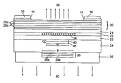
- FIG. 1 shows a first embodiment of the invention.
- the current is supplied through the lower p contact ( 25 ), which simultaneously operates as an integrated heat sink, and the n-contacts ( 10 ), which may optionally be applied to a highly doped contact layer ( 11 ).
- the light escapes upwards ( 50 ) while the heat is removed downwards ( 60 ) through the integrated heat sink ( 25 ), e.g., onto a copper housing.
- the active laser region ( 26 ) is situated within the active layer ( 22 ), which preferably consists of a braced multi-layer structure (Multi-quantum well: MQW structure).
- the lateral dimensions of the active laser region are determined by the flow of current through the structured tunnel contact or tunnel junction consisting of a highly p-doped layer ( 40 ) and a highly n-doped layer ( 41 ), which is laterally circular in structure, for example (diameter W), and by the lateral expansion of the current in the layer ( 23 ) and the charge carrier diffusion in the active layer ( 22 ).
- the vertical limit of the electrons and holes injected into the active region is provided by the n- and p-doped boundary layers ( 21 ) and ( 23 ), respectively.
- the mirror ( 20 ) produced epitaxially according to the prior art and consisting for example of a plurality (e.g., 36) of ⁇ / 4 pairs of layers of two semiconductor materials ( 20 a ) and ( 20 b ) with different refractive indices.
- the lower mirror ( 30 ) consists of several (e.g., 1.5 or 2.5) pairs of dielectric ⁇ / 4 pairs of layers ( 30 a ) and ( 30 b ), such as MgF2 ( 30 a ) and Si ( 30 b ), for example. Its reflectivity is additionally increased by the reflection on the lower interface with the integrated heat sink ( 25 ), particularly if the latter consists of highly reflective metals such as gold or silver.
- the tunnel contact In the vertical direction, the tunnel contact is placed in the minimum amount of the electromagnetic field so that there are no or only very negligible optical losses in the highly doped and absorbent layers ( 40 ) and ( 41 ). For the same reason the tunnel contact should be as thin as possible; favorable values for the total thickness D are 20 to 60 nm for 1.3 to 1.55 ⁇ m VCSEL.
- the second semiconductor layer ( 24 ) on the p side may be (highly) n-doped by virtue of the tunnel contact or may have a gradient in the n doping with lower doping adjacent to the layer ( 23 ) and higher doping on the underside towards the mirror ( 30 ) and the integrated heat sink ( 25 ).
- the layer ( 24 ) should preferably have good thermal conductivity in order to improve and expand the flow of heat from the active region (e.g., to a multiple of the diameter S), thus giving the advantage of reduced overall heating.
- the lateral dimension S of the dielectric mirror is preferably selected to be at least as great as the lateral dimension W of the tunnel contact. It is particularly useful if the dimension S is about 3–8 ⁇ m greater than W (typically 2–20 ⁇ m for 1.3 ⁇ m and 1.55 ⁇ m VCSELs), since the lateral expansion of the optical field, as a result of the wave guiding by the amplification and thermal lensing of the active laser region ( 26 ), is restricted to roughly the dimension of the active laser region.
- FIG. 2 shows a second embodiment of the invention.
- the manufacturing process is such that the structure of the tunnel contact is imaged in the epitaxy overgrowing into the surface of the layer ( 24 ). This results in increased lateral wave guiding which is aligned precisely, in self-adjusting manner, with the tunnel contact and the active region ( 26 ).
- the imaging of the tunnel contact may be widened or reduced, thus allowing, the lateral limits of the optical field to be influenced over a wide range.
- This method may be combined with the structural variants described below in order to optimize laser properties.
- FIG. 3 shows a third embodiment of the invention. It is clearly emphasized here that the application of an additional highly reflective metallic layer ( 30 c ) onto the dielectric mirror ( 30 ) as a whole can produce high reflectivity which in this embodiment does not depend on the properties of the integrated heat sink and contact layer ( 25 ).
- FIG. 4 shows a fourth embodiment of the invention.
- the contact resistance to the contact layer ( 25 ) on the p side can be reduced by lateral insertion of a highly n-doped intermediate contact layer ( 70 ).
- the layer ( 24 ) may consist of thermally highly conductive n-doped InP and the intermediate contact layer ( 70 ) may consist of highly n-doped InGaAs, which produces very low contact resistances.
- FIG. 5 shows a fifth embodiment of the invention in which both low-impedance contact by means of the intermediate contact layer ( 70 ) and also a good discharge of heat through the window ( 71 ) are made possible by the fact that an intermediate space is provided between the dielectric mirror ( 30 ) and the intermediate contact layer ( 70 ), through which the heat is able to flow away.
- the lateral width of the region ( 71 ) is therefore preferably greater than the thickness of the layer ( 24 ).
- FIG. 6 shows three process steps for producing a diffusion barrier according to a first embodiment.
- a diffusion barrier 601 is applied to a first area, while a second area 602 is masked.
- the diffusion barrier may consist of platinum (Pt), for example.
- Pt platinum
- a layer of titanium may be applied underneath the layer of platinum.
- a layer of gold may be applied to the layer of platinum.
- the diffusion barrier then consists of layers of Ti/Pt/Au.
- a dielectric mirror 603 is applied in the second region 602 .
- a certain overlap with the diffusion barrier 601 may be allowed at the points 605 , 606 .
- the advantage of this overlap is that a tight seal can be guaranteed between the dielectric mirror and the diffusion barrier so as to safely rule out any possibility of diffusion from the contact layer into the n-doped semiconductor layer.
- a layer of gold 604 is applied to the dielectric mirror 603 .
- FIG. 7 shows three process steps for the preparation of a diffusion barrier according to a second embodiment.
- the main difference from the process steps according to FIG. 6 is that, in a first process step (a), first of all a dielectric mirror is applied and in a second process step (b) the diffusion barrier 702 is then applied which may in turn consist of the sequence of layers Ti/Pt/Au mentioned above. Then, in a third step (c), a layer of gold 703 is applied to the dielectric mirror.
- the masking is precisely adjusted so as to prevent diffusion between the dielectric mirror and the n-doped semiconductor layer underneath it, as before.
- Table 1 lists some exemplary data for a semiconductor diode according to the invention, the numbers in the first column referring to the reference numerals in the figures.
Landscapes
- Physics & Mathematics (AREA)
- Condensed Matter Physics & Semiconductors (AREA)
- General Physics & Mathematics (AREA)
- Electromagnetism (AREA)
- Optics & Photonics (AREA)
- Semiconductor Lasers (AREA)
Applications Claiming Priority (3)
| Application Number | Priority Date | Filing Date | Title |
|---|---|---|---|
| DE10107349A DE10107349A1 (de) | 2001-02-15 | 2001-02-15 | Oberflächenemittierender Halbleiterlaser |
| DE10107349.6 | 2001-02-15 | ||
| PCT/EP2002/001656 WO2002065599A2 (de) | 2001-02-15 | 2002-02-15 | Oberflächenemittierender halbleiterlaser |
Publications (2)
| Publication Number | Publication Date |
|---|---|
| US20040179568A1 US20040179568A1 (en) | 2004-09-16 |
| US7170917B2 true US7170917B2 (en) | 2007-01-30 |
Family
ID=7674324
Family Applications (1)
| Application Number | Title | Priority Date | Filing Date |
|---|---|---|---|
| US10/468,183 Expired - Lifetime US7170917B2 (en) | 2001-02-15 | 2002-02-15 | Surface-emitting semiconductor laser |
Country Status (12)
| Country | Link |
|---|---|
| US (1) | US7170917B2 (enExample) |
| EP (1) | EP1366548B1 (enExample) |
| JP (1) | JP2004535058A (enExample) |
| KR (1) | KR100626891B1 (enExample) |
| CN (1) | CN1263207C (enExample) |
| AT (1) | ATE294457T1 (enExample) |
| CA (1) | CA2438341A1 (enExample) |
| DE (2) | DE10107349A1 (enExample) |
| DK (1) | DK1366548T3 (enExample) |
| ES (1) | ES2240725T3 (enExample) |
| IL (1) | IL157362A0 (enExample) |
| WO (1) | WO2002065599A2 (enExample) |
Cited By (3)
| Publication number | Priority date | Publication date | Assignee | Title |
|---|---|---|---|---|
| US20060249738A1 (en) * | 2003-10-16 | 2006-11-09 | Markus Ortsiefer | Surface-emitting semiconductor laser comprising a structured waveguide |
| US10033158B1 (en) | 2016-12-19 | 2018-07-24 | Osram Opto Semiconductors Gmbh | Semiconductor laser, laser assembly and method of making a semiconductor laser |
| CN114498285A (zh) * | 2022-01-24 | 2022-05-13 | 中国科学院半导体研究所 | 一种半导体激光器 |
Families Citing this family (16)
| Publication number | Priority date | Publication date | Assignee | Title |
|---|---|---|---|---|
| DE10107349A1 (de) | 2001-02-15 | 2002-08-29 | Markus-Christian Amann | Oberflächenemittierender Halbleiterlaser |
| DE10147888A1 (de) * | 2001-09-28 | 2003-04-24 | Osram Opto Semiconductors Gmbh | Optisch gepumpter vertikal emittierender Halbleiterlaser |
| DE10305079B4 (de) * | 2002-11-27 | 2005-04-28 | Vertilas Gmbh | Verfahren zur Herstellung eines vergrabenen Tunnelkontakts in einem oberflächenemittierenden Halbleiterlaser sowie oberflächenemittierender Halbleiterlaser |
| US6936486B2 (en) * | 2002-11-19 | 2005-08-30 | Jdsu Uniphase Corporation | Low voltage multi-junction vertical cavity surface emitting laser |
| JP2006508550A (ja) * | 2002-11-27 | 2006-03-09 | フェルティラス ゲーエムベーハー | 面発光型半導体レーザの埋込トンネル接合の製造方法 |
| US6870868B2 (en) * | 2003-02-18 | 2005-03-22 | Eastman Kodak Company | Organic laser having improved linearity |
| US7372886B2 (en) * | 2004-06-07 | 2008-05-13 | Avago Technologies Fiber Ip Pte Ltd | High thermal conductivity vertical cavity surface emitting laser (VCSEL) |
| JP2008198957A (ja) * | 2007-02-16 | 2008-08-28 | Hitachi Ltd | 半導体レーザ装置および光増幅装置 |
| JPWO2008114707A1 (ja) | 2007-03-22 | 2010-07-01 | 日本電気株式会社 | 面発光型半導体レーザ |
| JP2012119408A (ja) * | 2010-11-30 | 2012-06-21 | Nippon Telegr & Teleph Corp <Ntt> | 半導体素子、半導体光素子及び半導体集積素子 |
| KR20130132064A (ko) * | 2012-05-25 | 2013-12-04 | (주)파이버피아 | 수직 면발광 레이저다이오드 |
| CN106856296B (zh) * | 2016-12-27 | 2019-07-05 | 中国科学院半导体研究所 | 一种长波长垂直腔面发射激光器 |
| CN108927601A (zh) * | 2018-07-18 | 2018-12-04 | 张家港市顶峰激光科技有限公司 | 一种利用半导体激光束进行材料表面整平设备 |
| US11695093B2 (en) | 2018-11-21 | 2023-07-04 | Analog Devices, Inc. | Superlattice photodetector/light emitting diode |
| US12272924B2 (en) | 2022-12-12 | 2025-04-08 | Bandwidth10, LTD. | HCG tunable VCSEL system with ASIC for processing information and firmware |
| US12483003B2 (en) | 2022-12-12 | 2025-11-25 | Bandwidth10, LTD. | HCG tunable VCSEL with integrated detector in the sacrificial layer |
Citations (7)
| Publication number | Priority date | Publication date | Assignee | Title |
|---|---|---|---|---|
| EP0184117A2 (de) | 1984-12-03 | 1986-06-11 | Siemens Aktiengesellschaft | Strahlung erzeugende Halbleiterdiode mit einem kleinflächigen Kontakt mit grossflächigerem Oberflächenschutz |
| US5661075A (en) | 1995-02-06 | 1997-08-26 | Motorola | Method of making a VCSEL with passivation |
| WO1998007218A1 (en) | 1996-08-09 | 1998-02-19 | W.L. Gore & Associates, Inc. | Vertical cavity surface emitting laser with tunnel junction |
| US5831295A (en) * | 1995-12-01 | 1998-11-03 | Motorola, Inc. | Current confinement via defect generator and hetero-interface interaction |
| US5936266A (en) * | 1997-07-22 | 1999-08-10 | The Board Of Trustees Of The University Of Illinois | Semiconductor devices and methods with tunnel contact hole sources |
| US6052398A (en) | 1997-04-03 | 2000-04-18 | Alcatel | Surface emitting semiconductor laser |
| DE10107349A1 (de) | 2001-02-15 | 2002-08-29 | Markus-Christian Amann | Oberflächenemittierender Halbleiterlaser |
-
2001
- 2001-02-15 DE DE10107349A patent/DE10107349A1/de not_active Withdrawn
-
2002
- 2002-02-15 WO PCT/EP2002/001656 patent/WO2002065599A2/de not_active Ceased
- 2002-02-15 US US10/468,183 patent/US7170917B2/en not_active Expired - Lifetime
- 2002-02-15 DE DE50202912T patent/DE50202912D1/de not_active Expired - Lifetime
- 2002-02-15 IL IL15736202A patent/IL157362A0/xx unknown
- 2002-02-15 CN CNB028050193A patent/CN1263207C/zh not_active Expired - Fee Related
- 2002-02-15 EP EP02719854A patent/EP1366548B1/de not_active Expired - Lifetime
- 2002-02-15 JP JP2002564807A patent/JP2004535058A/ja active Pending
- 2002-02-15 CA CA002438341A patent/CA2438341A1/en not_active Abandoned
- 2002-02-15 KR KR1020037010705A patent/KR100626891B1/ko not_active Expired - Fee Related
- 2002-02-15 DK DK02719854T patent/DK1366548T3/da active
- 2002-02-15 ES ES02719854T patent/ES2240725T3/es not_active Expired - Lifetime
- 2002-02-15 AT AT02719854T patent/ATE294457T1/de not_active IP Right Cessation
Patent Citations (7)
| Publication number | Priority date | Publication date | Assignee | Title |
|---|---|---|---|---|
| EP0184117A2 (de) | 1984-12-03 | 1986-06-11 | Siemens Aktiengesellschaft | Strahlung erzeugende Halbleiterdiode mit einem kleinflächigen Kontakt mit grossflächigerem Oberflächenschutz |
| US5661075A (en) | 1995-02-06 | 1997-08-26 | Motorola | Method of making a VCSEL with passivation |
| US5831295A (en) * | 1995-12-01 | 1998-11-03 | Motorola, Inc. | Current confinement via defect generator and hetero-interface interaction |
| WO1998007218A1 (en) | 1996-08-09 | 1998-02-19 | W.L. Gore & Associates, Inc. | Vertical cavity surface emitting laser with tunnel junction |
| US6052398A (en) | 1997-04-03 | 2000-04-18 | Alcatel | Surface emitting semiconductor laser |
| US5936266A (en) * | 1997-07-22 | 1999-08-10 | The Board Of Trustees Of The University Of Illinois | Semiconductor devices and methods with tunnel contact hole sources |
| DE10107349A1 (de) | 2001-02-15 | 2002-08-29 | Markus-Christian Amann | Oberflächenemittierender Halbleiterlaser |
Non-Patent Citations (6)
| Title |
|---|
| Liau, Z.L., et al: "A Novel Technique For Gainasp/Inp Buried Heterostructure Laser Fabrication" Applied Physics Letters, American Institute of Physics, New York, US, p. 568-570, Apr. 1, 1982. |
| Nakagawa, S., et al.: "88° Continuous-Wave Operation Of Apertured, Intracavity Contacted, 1.55 Mum Vertical-Cavity Surface-Emitting Lasers" Applied Physics Letters, American Institute of Physics, New York, US, p. 1337-1339, Mar. 5, 2001. |
| Ortsiefer, M, et al.: "Low-Threshold Index-Guided 1.5 Mum Long-Wavelenght Vertical-Cavity Surface-Emitting Laser With High Efficiency", Applied Physics Letters, American Institute of Physics, New York, US, p. 2179-2181, Apr. 17, 2000. |
| Ortsiefer, M, et al: "90° C Continuous-Wave Operation Of 1.83-Mum Vertical-Cavity Surface-Emitting Lasers" IEEE Photonics Technology Letters, IEE Inc., New York, US, pp. 1435-1437, Nov. 2000. |
| Ortsiefer, M., et al: "Submilliamp Long-Wavelength InP-Based Vertical-Cavity Surface-Emitting Laser With Stable Linear Polarisation" Electronics Letters, IEE Stevenage, p. 1124-1126, Jun. 22, 2000. |
| Schraud, G, et al: "Substrateless Singlemode Vertical Cavity Surface-Emitting GaAs/GaALAs Laser Diode" Electronics Letters, IEE Stevenage, GB, pp. 238-239, Feb. 3, 1994. |
Cited By (5)
| Publication number | Priority date | Publication date | Assignee | Title |
|---|---|---|---|---|
| US20060249738A1 (en) * | 2003-10-16 | 2006-11-09 | Markus Ortsiefer | Surface-emitting semiconductor laser comprising a structured waveguide |
| US7700941B2 (en) * | 2003-10-16 | 2010-04-20 | Vertilas Gmbh | Surface-emitting semiconductor laser comprising a structured waveguide |
| US10033158B1 (en) | 2016-12-19 | 2018-07-24 | Osram Opto Semiconductors Gmbh | Semiconductor laser, laser assembly and method of making a semiconductor laser |
| CN114498285A (zh) * | 2022-01-24 | 2022-05-13 | 中国科学院半导体研究所 | 一种半导体激光器 |
| CN114498285B (zh) * | 2022-01-24 | 2024-02-06 | 中国科学院半导体研究所 | 一种半导体激光器 |
Also Published As
| Publication number | Publication date |
|---|---|
| WO2002065599A3 (de) | 2002-10-24 |
| CN1491468A (zh) | 2004-04-21 |
| JP2004535058A (ja) | 2004-11-18 |
| IL157362A0 (en) | 2004-02-19 |
| CN1263207C (zh) | 2006-07-05 |
| CA2438341A1 (en) | 2002-08-22 |
| EP1366548B1 (de) | 2005-04-27 |
| DE50202912D1 (de) | 2005-06-02 |
| ES2240725T3 (es) | 2005-10-16 |
| ATE294457T1 (de) | 2005-05-15 |
| WO2002065599A2 (de) | 2002-08-22 |
| KR100626891B1 (ko) | 2006-09-20 |
| KR20030084928A (ko) | 2003-11-01 |
| DK1366548T3 (da) | 2005-06-27 |
| DE10107349A1 (de) | 2002-08-29 |
| EP1366548A2 (de) | 2003-12-03 |
| US20040179568A1 (en) | 2004-09-16 |
Similar Documents
| Publication | Publication Date | Title |
|---|---|---|
| US7170917B2 (en) | Surface-emitting semiconductor laser | |
| US4943970A (en) | Surface emitting laser | |
| US5724376A (en) | Transparent substrate vertical cavity surface emitting lasers fabricated by semiconductor wafer bonding | |
| US4901327A (en) | Transverse injection surface emitting laser | |
| US6687281B2 (en) | Double intracavity contacted long-wavelength VCSELs | |
| EP1208622B1 (en) | Coupled cavity anti-guided vertical cavity surface emitting laser (vcsel) | |
| JPH10321952A (ja) | 表面放射半導体レーザ | |
| JPS61127192A (ja) | 表面放射発光装置 | |
| WO1992000610A1 (en) | Quantum well device with control of spontaneous photon emission, and method of manufacturing same | |
| JP2004146833A (ja) | 複数活性領域を備えた電気ポンピング式垂直共振器面発光レーザ | |
| US6904072B2 (en) | Vertical cavity surface emitting laser having a gain guide aperture interior to an oxide confinement layer | |
| JP2012505541A (ja) | 改善したモード選択度を持つ垂直キャビティ面発光レーザー | |
| JP2000196189A (ja) | 面発光型半導体レーザ | |
| GB2347559A (en) | Wafer bonded vertical cavity surface emitting lasers | |
| US20060126687A1 (en) | Method for producing a buried tunnel junction in a surface-emitting semiconductor laser | |
| US7376163B2 (en) | Method for producing a waveguide structure in a surface-emitting semiconductor laser and surface-emitting semiconductor laser | |
| US6977424B1 (en) | Electrically pumped semiconductor active region with a backward diode, for enhancing optical signals | |
| Chua et al. | Low-threshold InAlGaAs vertical-cavity surface-emitting laser arrays using transparent contacts | |
| JP2024070244A (ja) | 多接合底面発光型垂直キャビティ面発光レーザーおよびその製造方法 | |
| KR940010166B1 (ko) | 표면방출형 반도체 레이저 다이오드의 제조방법 | |
| JPS6395689A (ja) | 半導体発光装置 | |
| JPH03148892A (ja) | 面発光レーザ発振装置 | |
| JPS6212182A (ja) | 半導体レ−ザ |
Legal Events
| Date | Code | Title | Description |
|---|---|---|---|
| AS | Assignment |
Owner name: VERTILAS GMBH, GERMANY Free format text: ASSIGNMENT OF ASSIGNORS INTEREST;ASSIGNORS:AMANN, MARKUS-CHRISTIAN;ORTSIEFFER, MARKUS;REEL/FRAME:015352/0888 Effective date: 20040323 |
|
| STCF | Information on status: patent grant |
Free format text: PATENTED CASE |
|
| CC | Certificate of correction | ||
| FPAY | Fee payment |
Year of fee payment: 4 |
|
| FEPP | Fee payment procedure |
Free format text: PAT HOLDER CLAIMS SMALL ENTITY STATUS, ENTITY STATUS SET TO SMALL (ORIGINAL EVENT CODE: LTOS); ENTITY STATUS OF PATENT OWNER: SMALL ENTITY |
|
| FPAY | Fee payment |
Year of fee payment: 8 |
|
| MAFP | Maintenance fee payment |
Free format text: PAYMENT OF MAINTENANCE FEE, 12TH YR, SMALL ENTITY (ORIGINAL EVENT CODE: M2553) Year of fee payment: 12 |
|
| AS | Assignment |
Owner name: SOUND POINT AGENCY LLC, NEW YORK Free format text: SECURITY INTEREST;ASSIGNORS:LUMILEDS LLC;LUMILEDS HOLDING B.V.;REEL/FRAME:062299/0338 Effective date: 20221230 |