EP1366548B1 - Oberflächenemittierender halbleiterlaser - Google Patents
Oberflächenemittierender halbleiterlaser Download PDFInfo
- Publication number
- EP1366548B1 EP1366548B1 EP02719854A EP02719854A EP1366548B1 EP 1366548 B1 EP1366548 B1 EP 1366548B1 EP 02719854 A EP02719854 A EP 02719854A EP 02719854 A EP02719854 A EP 02719854A EP 1366548 B1 EP1366548 B1 EP 1366548B1
- Authority
- EP
- European Patent Office
- Prior art keywords
- layer
- diffusion barrier
- dielectric mirror
- contact
- active zone
- Prior art date
- Legal status (The legal status is an assumption and is not a legal conclusion. Google has not performed a legal analysis and makes no representation as to the accuracy of the status listed.)
- Expired - Lifetime
Links
- 239000004065 semiconductor Substances 0.000 title claims abstract description 80
- 238000009792 diffusion process Methods 0.000 claims abstract description 45
- 230000004888 barrier function Effects 0.000 claims abstract description 42
- 230000007704 transition Effects 0.000 claims abstract description 8
- 238000000034 method Methods 0.000 claims description 24
- BASFCYQUMIYNBI-UHFFFAOYSA-N platinum Chemical compound [Pt] BASFCYQUMIYNBI-UHFFFAOYSA-N 0.000 claims description 17
- 230000008569 process Effects 0.000 claims description 13
- 239000010936 titanium Substances 0.000 claims description 8
- 229910052697 platinum Inorganic materials 0.000 claims description 6
- 238000002310 reflectometry Methods 0.000 claims description 5
- RTAQQCXQSZGOHL-UHFFFAOYSA-N Titanium Chemical compound [Ti] RTAQQCXQSZGOHL-UHFFFAOYSA-N 0.000 claims description 4
- 229910052719 titanium Inorganic materials 0.000 claims description 4
- 239000002318 adhesion promoter Substances 0.000 claims 4
- 230000007774 longterm Effects 0.000 abstract description 4
- 239000010931 gold Substances 0.000 description 14
- PCHJSUWPFVWCPO-UHFFFAOYSA-N gold Chemical compound [Au] PCHJSUWPFVWCPO-UHFFFAOYSA-N 0.000 description 10
- 229910052737 gold Inorganic materials 0.000 description 10
- 239000000463 material Substances 0.000 description 8
- 238000004519 manufacturing process Methods 0.000 description 7
- 239000000243 solution Substances 0.000 description 7
- 230000003287 optical effect Effects 0.000 description 5
- 229910000530 Gallium indium arsenide Inorganic materials 0.000 description 4
- 230000008901 benefit Effects 0.000 description 4
- 229910052709 silver Inorganic materials 0.000 description 4
- 239000004332 silver Substances 0.000 description 4
- 239000013078 crystal Substances 0.000 description 3
- 238000000605 extraction Methods 0.000 description 3
- 230000017525 heat dissipation Effects 0.000 description 3
- 238000005215 recombination Methods 0.000 description 3
- 230000006798 recombination Effects 0.000 description 3
- 239000000758 substrate Substances 0.000 description 3
- 230000005641 tunneling Effects 0.000 description 3
- 229910001218 Gallium arsenide Inorganic materials 0.000 description 2
- 239000002019 doping agent Substances 0.000 description 2
- 230000002349 favourable effect Effects 0.000 description 2
- 238000002513 implantation Methods 0.000 description 2
- 238000002347 injection Methods 0.000 description 2
- 239000007924 injection Substances 0.000 description 2
- 229910052751 metal Inorganic materials 0.000 description 2
- 239000002184 metal Substances 0.000 description 2
- 230000006641 stabilisation Effects 0.000 description 2
- RYGMFSIKBFXOCR-UHFFFAOYSA-N Copper Chemical compound [Cu] RYGMFSIKBFXOCR-UHFFFAOYSA-N 0.000 description 1
- 229910000673 Indium arsenide Inorganic materials 0.000 description 1
- 208000012868 Overgrowth Diseases 0.000 description 1
- 239000000853 adhesive Substances 0.000 description 1
- 230000001070 adhesive effect Effects 0.000 description 1
- 230000015572 biosynthetic process Effects 0.000 description 1
- 230000000903 blocking effect Effects 0.000 description 1
- 239000002800 charge carrier Substances 0.000 description 1
- 239000003795 chemical substances by application Substances 0.000 description 1
- 230000001427 coherent effect Effects 0.000 description 1
- 229910052802 copper Inorganic materials 0.000 description 1
- 239000010949 copper Substances 0.000 description 1
- 230000001419 dependent effect Effects 0.000 description 1
- 230000000694 effects Effects 0.000 description 1
- 230000005672 electromagnetic field Effects 0.000 description 1
- 230000020169 heat generation Effects 0.000 description 1
- 238000010438 heat treatment Methods 0.000 description 1
- 230000006872 improvement Effects 0.000 description 1
- RPQDHPTXJYYUPQ-UHFFFAOYSA-N indium arsenide Chemical compound [In]#[As] RPQDHPTXJYYUPQ-UHFFFAOYSA-N 0.000 description 1
- 238000002955 isolation Methods 0.000 description 1
- 230000000873 masking effect Effects 0.000 description 1
- 150000002739 metals Chemical class 0.000 description 1
- 230000035699 permeability Effects 0.000 description 1
- 238000002360 preparation method Methods 0.000 description 1
- 230000002787 reinforcement Effects 0.000 description 1
- 230000003595 spectral effect Effects 0.000 description 1
- 238000011105 stabilization Methods 0.000 description 1
- 239000007858 starting material Substances 0.000 description 1
Images
Classifications
-
- H—ELECTRICITY
- H01—ELECTRIC ELEMENTS
- H01S—DEVICES USING THE PROCESS OF LIGHT AMPLIFICATION BY STIMULATED EMISSION OF RADIATION [LASER] TO AMPLIFY OR GENERATE LIGHT; DEVICES USING STIMULATED EMISSION OF ELECTROMAGNETIC RADIATION IN WAVE RANGES OTHER THAN OPTICAL
- H01S5/00—Semiconductor lasers
- H01S5/10—Construction or shape of the optical resonator, e.g. extended or external cavity, coupled cavities, bent-guide, varying width, thickness or composition of the active region
- H01S5/18—Surface-emitting [SE] lasers, e.g. having both horizontal and vertical cavities
- H01S5/183—Surface-emitting [SE] lasers, e.g. having both horizontal and vertical cavities having only vertical cavities, e.g. vertical cavity surface-emitting lasers [VCSEL]
- H01S5/18361—Structure of the reflectors, e.g. hybrid mirrors
- H01S5/18369—Structure of the reflectors, e.g. hybrid mirrors based on dielectric materials
-
- H—ELECTRICITY
- H01—ELECTRIC ELEMENTS
- H01S—DEVICES USING THE PROCESS OF LIGHT AMPLIFICATION BY STIMULATED EMISSION OF RADIATION [LASER] TO AMPLIFY OR GENERATE LIGHT; DEVICES USING STIMULATED EMISSION OF ELECTROMAGNETIC RADIATION IN WAVE RANGES OTHER THAN OPTICAL
- H01S5/00—Semiconductor lasers
- H01S5/04—Processes or apparatus for excitation, e.g. pumping, e.g. by electron beams
- H01S5/042—Electrical excitation ; Circuits therefor
- H01S5/0425—Electrodes, e.g. characterised by the structure
- H01S5/04252—Electrodes, e.g. characterised by the structure characterised by the material
-
- H—ELECTRICITY
- H01—ELECTRIC ELEMENTS
- H01S—DEVICES USING THE PROCESS OF LIGHT AMPLIFICATION BY STIMULATED EMISSION OF RADIATION [LASER] TO AMPLIFY OR GENERATE LIGHT; DEVICES USING STIMULATED EMISSION OF ELECTROMAGNETIC RADIATION IN WAVE RANGES OTHER THAN OPTICAL
- H01S5/00—Semiconductor lasers
- H01S5/02—Structural details or components not essential to laser action
- H01S5/0206—Substrates, e.g. growth, shape, material, removal or bonding
- H01S5/0217—Removal of the substrate
-
- H—ELECTRICITY
- H01—ELECTRIC ELEMENTS
- H01S—DEVICES USING THE PROCESS OF LIGHT AMPLIFICATION BY STIMULATED EMISSION OF RADIATION [LASER] TO AMPLIFY OR GENERATE LIGHT; DEVICES USING STIMULATED EMISSION OF ELECTROMAGNETIC RADIATION IN WAVE RANGES OTHER THAN OPTICAL
- H01S5/00—Semiconductor lasers
- H01S5/02—Structural details or components not essential to laser action
- H01S5/024—Arrangements for thermal management
- H01S5/02476—Heat spreaders, i.e. improving heat flow between laser chip and heat dissipating elements
-
- H—ELECTRICITY
- H01—ELECTRIC ELEMENTS
- H01S—DEVICES USING THE PROCESS OF LIGHT AMPLIFICATION BY STIMULATED EMISSION OF RADIATION [LASER] TO AMPLIFY OR GENERATE LIGHT; DEVICES USING STIMULATED EMISSION OF ELECTROMAGNETIC RADIATION IN WAVE RANGES OTHER THAN OPTICAL
- H01S5/00—Semiconductor lasers
- H01S5/04—Processes or apparatus for excitation, e.g. pumping, e.g. by electron beams
- H01S5/042—Electrical excitation ; Circuits therefor
- H01S5/0421—Electrical excitation ; Circuits therefor characterised by the semiconducting contacting layers
-
- H—ELECTRICITY
- H01—ELECTRIC ELEMENTS
- H01S—DEVICES USING THE PROCESS OF LIGHT AMPLIFICATION BY STIMULATED EMISSION OF RADIATION [LASER] TO AMPLIFY OR GENERATE LIGHT; DEVICES USING STIMULATED EMISSION OF ELECTROMAGNETIC RADIATION IN WAVE RANGES OTHER THAN OPTICAL
- H01S5/00—Semiconductor lasers
- H01S5/04—Processes or apparatus for excitation, e.g. pumping, e.g. by electron beams
- H01S5/042—Electrical excitation ; Circuits therefor
- H01S5/0425—Electrodes, e.g. characterised by the structure
- H01S5/04252—Electrodes, e.g. characterised by the structure characterised by the material
- H01S5/04253—Electrodes, e.g. characterised by the structure characterised by the material having specific optical properties, e.g. transparent electrodes
-
- H—ELECTRICITY
- H01—ELECTRIC ELEMENTS
- H01S—DEVICES USING THE PROCESS OF LIGHT AMPLIFICATION BY STIMULATED EMISSION OF RADIATION [LASER] TO AMPLIFY OR GENERATE LIGHT; DEVICES USING STIMULATED EMISSION OF ELECTROMAGNETIC RADIATION IN WAVE RANGES OTHER THAN OPTICAL
- H01S5/00—Semiconductor lasers
- H01S5/10—Construction or shape of the optical resonator, e.g. extended or external cavity, coupled cavities, bent-guide, varying width, thickness or composition of the active region
- H01S5/18—Surface-emitting [SE] lasers, e.g. having both horizontal and vertical cavities
- H01S5/183—Surface-emitting [SE] lasers, e.g. having both horizontal and vertical cavities having only vertical cavities, e.g. vertical cavity surface-emitting lasers [VCSEL]
- H01S5/18308—Surface-emitting [SE] lasers, e.g. having both horizontal and vertical cavities having only vertical cavities, e.g. vertical cavity surface-emitting lasers [VCSEL] having a special structure for lateral current or light confinement
-
- H—ELECTRICITY
- H01—ELECTRIC ELEMENTS
- H01S—DEVICES USING THE PROCESS OF LIGHT AMPLIFICATION BY STIMULATED EMISSION OF RADIATION [LASER] TO AMPLIFY OR GENERATE LIGHT; DEVICES USING STIMULATED EMISSION OF ELECTROMAGNETIC RADIATION IN WAVE RANGES OTHER THAN OPTICAL
- H01S5/00—Semiconductor lasers
- H01S5/10—Construction or shape of the optical resonator, e.g. extended or external cavity, coupled cavities, bent-guide, varying width, thickness or composition of the active region
- H01S5/18—Surface-emitting [SE] lasers, e.g. having both horizontal and vertical cavities
- H01S5/183—Surface-emitting [SE] lasers, e.g. having both horizontal and vertical cavities having only vertical cavities, e.g. vertical cavity surface-emitting lasers [VCSEL]
- H01S5/18361—Structure of the reflectors, e.g. hybrid mirrors
- H01S5/18375—Structure of the reflectors, e.g. hybrid mirrors based on metal reflectors
-
- H—ELECTRICITY
- H01—ELECTRIC ELEMENTS
- H01S—DEVICES USING THE PROCESS OF LIGHT AMPLIFICATION BY STIMULATED EMISSION OF RADIATION [LASER] TO AMPLIFY OR GENERATE LIGHT; DEVICES USING STIMULATED EMISSION OF ELECTROMAGNETIC RADIATION IN WAVE RANGES OTHER THAN OPTICAL
- H01S5/00—Semiconductor lasers
- H01S5/10—Construction or shape of the optical resonator, e.g. extended or external cavity, coupled cavities, bent-guide, varying width, thickness or composition of the active region
- H01S5/18—Surface-emitting [SE] lasers, e.g. having both horizontal and vertical cavities
- H01S5/183—Surface-emitting [SE] lasers, e.g. having both horizontal and vertical cavities having only vertical cavities, e.g. vertical cavity surface-emitting lasers [VCSEL]
- H01S5/18361—Structure of the reflectors, e.g. hybrid mirrors
- H01S5/18377—Structure of the reflectors, e.g. hybrid mirrors comprising layers of different kind of materials, e.g. combinations of semiconducting with dielectric or metallic layers
-
- H—ELECTRICITY
- H01—ELECTRIC ELEMENTS
- H01S—DEVICES USING THE PROCESS OF LIGHT AMPLIFICATION BY STIMULATED EMISSION OF RADIATION [LASER] TO AMPLIFY OR GENERATE LIGHT; DEVICES USING STIMULATED EMISSION OF ELECTROMAGNETIC RADIATION IN WAVE RANGES OTHER THAN OPTICAL
- H01S5/00—Semiconductor lasers
- H01S5/30—Structure or shape of the active region; Materials used for the active region
- H01S5/305—Structure or shape of the active region; Materials used for the active region characterised by the doping materials used in the laser structure
- H01S5/3072—Diffusion blocking layer, i.e. a special layer blocking diffusion of dopants
-
- H—ELECTRICITY
- H01—ELECTRIC ELEMENTS
- H01S—DEVICES USING THE PROCESS OF LIGHT AMPLIFICATION BY STIMULATED EMISSION OF RADIATION [LASER] TO AMPLIFY OR GENERATE LIGHT; DEVICES USING STIMULATED EMISSION OF ELECTROMAGNETIC RADIATION IN WAVE RANGES OTHER THAN OPTICAL
- H01S5/00—Semiconductor lasers
- H01S5/30—Structure or shape of the active region; Materials used for the active region
- H01S5/305—Structure or shape of the active region; Materials used for the active region characterised by the doping materials used in the laser structure
- H01S5/3095—Tunnel junction
Definitions
- the invention relates to a semiconductor laser of surface emitting type having a pn junction having active zone as well as a method for Production of a diffusion barrier in such a Semiconductor lasers.
- Semiconductor lasers are in principle one in the flow direction operated semiconductor diode, which stimulated by Emission coherent, spectral narrowband light generated and directed radiates.
- the for the laser process necessary population inversion is by a Current injection into the pn junction achieved.
- supporting measure can be a high doping of the Be provided starting material.
- the induced radiative recombination In the area of the pn junction, in which the electrons and holes are spatially be present adjacent, then the induced radiative recombination.
- the optical resonator is in the simplest case of two opposite, perpendicular to the pn junction formed by optical mirrors. In this design finds one Emission in the plane perpendicular to the current injection instead.
- VCSEL vertical-cavity surface-emitting laser diode
- US 6 052 398 is a semiconductor laser of Surface emitting type known, the one structured tunneling contact, wherein the resonator is formed by two semiconductor mirrors. This consists the problem that heat over one of the mirrors must be dissipated, usually from ternary or quaternary mixed crystals with correspondingly worse exist thermal conductivity.
- the US calls 6 052 398 also the use of a dielectric mirror on the p side of the active zone without looking for this Alternative solution to be called special benefits. In the In practice, this solution is not used because reflective contact layers (usually gold or Silver) into the adjacent semiconductor layers can diffuse, so that long-term stability is not guaranteed.
- EP-A 0 184 117 deals with an LED diode and a Process for their preparation.
- the diode has a on small area contact, where below the Contact lying semiconductor material that portion (for example, by proton implantation) high impedance made in the area outside the boundary of the Contact lies.
- a semiconductor layer structure applied, wherein to prevent diffusion from the usually made of gold contact in this Semiconductor layers, a barrier layer is applied extends laterally over the entire area of the diode.
- the layer thickness of the barrier layer would have to be so large be that for the wavelengths of this question here upcoming semiconductor laser would be impermeable while they sufficient permeability for the mentioned Proton implantation still granted.
- the object of the invention is a semiconductor laser to provide that under normal ambient temperatures to operate and a stable long-term behavior having.
- a semiconductor laser with the Characteristics of claim 1 solved include the features of the invention a Surface-emitting type semiconductor laser, comprising a pn-junction having active zone, with a first n-doped semiconductor layer on the n-side of the active zone, with a structured tunneling contact the p-side of the active zone, which has a conductive transition to a second n-doped semiconductor layer on the p-side the active zone forms, with a structured dielectric mirror, which is on the second n-doped Semiconductor layer is applied, with a Contact layer, which makes contact with the second n-doped Semiconductor layer forms where the dielectric mirror is not applied, and with a diffusion barrier between the contact layer and the second n-doped Semiconductor layer, wherein the dielectric mirror, the Diffusion barrier partially overlapped.
- the solution according to the invention is based on the knowledge that on the p-side of the active zone, the n-doped there Semiconductor layer with both a dielectric Mirror, as well as with a diffusion barrier a contact layer is completed.
- the contact layer forms a heat sink and thus allows an effective Heat dissipation.
- the diffusion barrier therefore prevents together with the dielectric mirror that components from the contact layer into the second n-doped Semiconductor layer diffuse and worst case Fall into the active zone and there the radiant Suppress recombination. This is for the Material selection of the heat sink free hand, so that total a thermally optimized structure of a semiconductor laser can be realized.
- An inventive method for applying a Diffusion barrier consists of the characteristics of the Patent claim 9, wherein in a first area on the second n-doped semiconductor layer, the diffusion barrier is applied, in which in a second area on the second n-type semiconductor layer is a dielectric Mirror is applied such that the dielectric Mirror partially overlaps the diffusion barrier and wherein the contact layer at least over the Diffusion barrier is applied.
- the dielectric Mirror an alternating sequence of binary layers to provide such that the binary layers in the middle a good lattice match to the adjacent layers exhibit.
- the binary layers alternating between InAs and GaAs with layer thicknesses of each 3nm so that the mean lattice spacing of the binary layers with the adjacent semiconductor layer matches.
- the Diffusion barrier is between the Diffusion barrier and the second semiconductor layer Adhesive provided.
- the Adhesion agent while a titanium layer and the Diffusion barrier of a platinum layer.
- a metallic Be provided end layer can be provided.
- the metallic terminating layer consistently also between the diffusion barrier and the Contact layer may be provided.
- the dielectric mirror is made, for example, of a plurality of ⁇ / 4 dielectric layer pairs, preferably formed of materials having a large difference in refractive index, such as MgF 2 and Si.
- the dielectric Mirror one opposite the semiconductor materials has lower thermal resistance, as a result directed heat conduction is achieved.
- the second n-doped the semiconductor layer can be made of an InP semiconductor, for example consist.
- the contact layer applied so thick is that it acts as a heat sink.
- the contact layer Preferably is applied the contact layer over the entire surface and covered also the dielectric mirror.
- the thickness of the Contact layer may be, for example 10 microns.
- the light extraction on the n-side of the active zone takes place.
- this is the substrate located on the n side of the active zone.
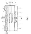
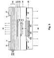
- Fig. 1 shows a first embodiment of the invention.
- the power supply via the lower p-contact (25), which also acts as an integrated heat sink, and the n-contacts (10), which are optional on a heavily doped Contact layer (11) may be applied.
- the n-contacts (10), which are optional on a heavily doped Contact layer (11) may be applied.
- the laser active Area (26) is inside the active layer (22), preferably made of a braced Multilayer structure exists (English: Multiquantumwell: MQW structure).
- the lateral dimensions of the laser-active Range is determined by the flow of current through the one highly p-doped layer (40) and a highly n-doped Layer (41) existing, laterally z.
- the epitaxially produced mirror (20) On the n-side there is the epitaxially produced mirror (20) according to the prior art, which consists for example of many (eg 36) ⁇ / 4-layer pairs of two semiconductor materials (20a) and (20b) with different refractive indices.
- the lower mirror (30) consists of several (eg 1.5 or 2.5) pairs of dielectric ⁇ / 4-layer pairs (30a) and (30b), such as. MgF 2 (30a) and Si (30b). Its reflectivity is additionally increased by the reflection at the lower interface to the integrated heat sink (25), especially if it consists of highly reflective metals such as gold or silver.
- the tunnel contact In the vertical direction, the tunnel contact is in a Minimum of the electromagnetic field, so no or negligible optical losses in the highly doped and absorbing layers (41) and (42) occur. For the same reason, the tunnel contact should be as thin as possible; favorable values for the total thickness D be 20 to 60nm for 1.3-1.55 ⁇ m VCSEL.
- the second p-sided Semiconductor layer (24) may be due to the Tunnel contact (high) n-doped or a gradient in the n-doping with lower dopants at the Border to the layer (23) and higher dopants at the Bottom to the mirror (30) and the integrated heat sink (25).
- the layer (24) should preferably have good thermal conductivity own to the heat flow from the active area too improve and expand (eg to a multiple of the Diameter S) which gives the advantage of a reduced Total heating results.
- the lateral Dimension S of the dielectric mirror is preferably at least as large as the lateral dimension W of Tunnel contact selected. It is particularly favorable, the Dimension S about 3-8 ⁇ m larger than W (typ. 2-20 ⁇ m at 1.3 ⁇ m and 1.55 ⁇ m VCSELn), since the lateral Extension of the optical field due to the waveguide through the reinforcement and the thermal lens effect (Thermal lensing) of the laser active region (26) on about the dimension of the laser-active region is limited.
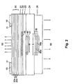
- Fig. 2 shows a second embodiment of the invention.
- the manufacturing process designed so that the structure of the tunnel contact at the epitaxial overgrowth in the layer surface of the Layer (24) maps. This creates a reinforced lateral waveguide, self-adjusting exactly to the tunnel contact and the active area (26) is aligned.
- the Illustration of the tunnel contact widened or reduced be, bringing the lateral boundary of the optical Fields can be influenced within wide limits.
- This method can be used to optimize the laser properties basically with the following Combine structural variants.
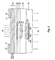
- Fig. 3 shows a third embodiment of the invention.
- an additional highly reflective metallic layer (30c) on the dielectric mirror (30) in total one high reflectivity can be achieved in this Not execution of the features of the integrated Heat sink and contact layer (25) depends.
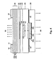
- Fig. 4 time a fourth embodiment of the invention.
- the p-side Contact resistance to the contact layer (25) by lateral Inserting a highly n-doped intermediate contact layer (70) be reduced.
- the layer (24) may consist of thermally well-conducting n-doped InP and the Intermediate contact layer (70) of highly n-doped InGaAs exist, which results in very low contact resistance.
- Fig. 5 shows a fifth embodiment of the Invention, in which both a low-resistance contact means the intermediate contact layer (70) as well as a good Heat dissipation through the window (71) is made possible by between the dielectric mirror (30) and the Intermediate contact layer (70) created a gap is, over which the heat can flow.
- the lateral Width of the region (71) is therefore preferably greater than the thickness of the layer (24).
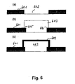
- Fig. 6 shows three process steps for the production of a Diffusion barrier according to one embodiment.
- a diffusion barrier 601 applied while a second area 602 is masked.
- the diffusion barrier can for example consist of platinum (Pt).
- Pt platinum
- a dielectric mirror 603 applied in the second area 602 .
- 606 can have a certain overlap with the diffusion barrier 601 are allowed.
- a third step (c) finally follows Applying a gold layer 604 to the dielectric Mirror 603.
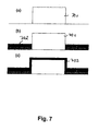
- Fig. 7 shows three process steps for the production of a Diffusion barrier according to one of the invention belonging example.
- a dielectric mirror is applied, while in a second process step (b) then the Applying the diffusion barrier 702 takes place, which in turn from the above-mentioned layer sequence Ti / Pt / Au can exist.
- a third process step (c) follows then again the application of a gold layer 703 on the dielectric mirror.
- the process sequence acc. Fig. 7 must be done an exact adjustment of the masking, so a diffusion between the dielectric mirror in the underneath n-doped semiconductor layer after is prevented before.
- Table 1 lists typical data for a semiconductor diode according to the invention, the numbers in the first column referring to the reference numbers in the figures.
- No. material Doping (cm -3 ) Thickness (nm) Diameter ( ⁇ m) comment 10 Ti: 10nm about 530 inside 55 Pt: 20nm outside 240 Au: 500nm 11 InGaAs n 5x10 19 100 inside 50 (lattice adjusted to InP) outside 250 20 20 a InGaAlAs (refractive index approx.
Landscapes
- Physics & Mathematics (AREA)
- Condensed Matter Physics & Semiconductors (AREA)
- General Physics & Mathematics (AREA)
- Electromagnetism (AREA)
- Optics & Photonics (AREA)
- Semiconductor Lasers (AREA)
Priority Applications (1)
| Application Number | Priority Date | Filing Date | Title |
|---|---|---|---|
| DK02719854T DK1366548T3 (da) | 2001-02-15 | 2002-02-15 | Overfladeemitterende halvlederlaser |
Applications Claiming Priority (3)
| Application Number | Priority Date | Filing Date | Title |
|---|---|---|---|
| DE10107349 | 2001-02-15 | ||
| DE10107349A DE10107349A1 (de) | 2001-02-15 | 2001-02-15 | Oberflächenemittierender Halbleiterlaser |
| PCT/EP2002/001656 WO2002065599A2 (de) | 2001-02-15 | 2002-02-15 | Oberflächenemittierender halbleiterlaser |
Publications (2)
| Publication Number | Publication Date |
|---|---|
| EP1366548A2 EP1366548A2 (de) | 2003-12-03 |
| EP1366548B1 true EP1366548B1 (de) | 2005-04-27 |
Family
ID=7674324
Family Applications (1)
| Application Number | Title | Priority Date | Filing Date |
|---|---|---|---|
| EP02719854A Expired - Lifetime EP1366548B1 (de) | 2001-02-15 | 2002-02-15 | Oberflächenemittierender halbleiterlaser |
Country Status (12)
| Country | Link |
|---|---|
| US (1) | US7170917B2 (enExample) |
| EP (1) | EP1366548B1 (enExample) |
| JP (1) | JP2004535058A (enExample) |
| KR (1) | KR100626891B1 (enExample) |
| CN (1) | CN1263207C (enExample) |
| AT (1) | ATE294457T1 (enExample) |
| CA (1) | CA2438341A1 (enExample) |
| DE (2) | DE10107349A1 (enExample) |
| DK (1) | DK1366548T3 (enExample) |
| ES (1) | ES2240725T3 (enExample) |
| IL (1) | IL157362A0 (enExample) |
| WO (1) | WO2002065599A2 (enExample) |
Families Citing this family (19)
| Publication number | Priority date | Publication date | Assignee | Title |
|---|---|---|---|---|
| DE10107349A1 (de) | 2001-02-15 | 2002-08-29 | Markus-Christian Amann | Oberflächenemittierender Halbleiterlaser |
| DE10147888A1 (de) * | 2001-09-28 | 2003-04-24 | Osram Opto Semiconductors Gmbh | Optisch gepumpter vertikal emittierender Halbleiterlaser |
| DE10305079B4 (de) * | 2002-11-27 | 2005-04-28 | Vertilas Gmbh | Verfahren zur Herstellung eines vergrabenen Tunnelkontakts in einem oberflächenemittierenden Halbleiterlaser sowie oberflächenemittierender Halbleiterlaser |
| US6936486B2 (en) * | 2002-11-19 | 2005-08-30 | Jdsu Uniphase Corporation | Low voltage multi-junction vertical cavity surface emitting laser |
| JP2006508550A (ja) * | 2002-11-27 | 2006-03-09 | フェルティラス ゲーエムベーハー | 面発光型半導体レーザの埋込トンネル接合の製造方法 |
| US6870868B2 (en) * | 2003-02-18 | 2005-03-22 | Eastman Kodak Company | Organic laser having improved linearity |
| DE10353960B4 (de) * | 2003-10-16 | 2006-03-23 | Vertilas Gmbh | Oberflächenemittierender Halbleiterlaser mit strukturiertem Wellenleiter |
| US7372886B2 (en) * | 2004-06-07 | 2008-05-13 | Avago Technologies Fiber Ip Pte Ltd | High thermal conductivity vertical cavity surface emitting laser (VCSEL) |
| JP2008198957A (ja) * | 2007-02-16 | 2008-08-28 | Hitachi Ltd | 半導体レーザ装置および光増幅装置 |
| JPWO2008114707A1 (ja) | 2007-03-22 | 2010-07-01 | 日本電気株式会社 | 面発光型半導体レーザ |
| JP2012119408A (ja) * | 2010-11-30 | 2012-06-21 | Nippon Telegr & Teleph Corp <Ntt> | 半導体素子、半導体光素子及び半導体集積素子 |
| KR20130132064A (ko) * | 2012-05-25 | 2013-12-04 | (주)파이버피아 | 수직 면발광 레이저다이오드 |
| US10033158B1 (en) | 2016-12-19 | 2018-07-24 | Osram Opto Semiconductors Gmbh | Semiconductor laser, laser assembly and method of making a semiconductor laser |
| CN106856296B (zh) * | 2016-12-27 | 2019-07-05 | 中国科学院半导体研究所 | 一种长波长垂直腔面发射激光器 |
| CN108927601A (zh) * | 2018-07-18 | 2018-12-04 | 张家港市顶峰激光科技有限公司 | 一种利用半导体激光束进行材料表面整平设备 |
| US11695093B2 (en) | 2018-11-21 | 2023-07-04 | Analog Devices, Inc. | Superlattice photodetector/light emitting diode |
| CN114498285B (zh) * | 2022-01-24 | 2024-02-06 | 中国科学院半导体研究所 | 一种半导体激光器 |
| US12272924B2 (en) | 2022-12-12 | 2025-04-08 | Bandwidth10, LTD. | HCG tunable VCSEL system with ASIC for processing information and firmware |
| US12483003B2 (en) | 2022-12-12 | 2025-11-25 | Bandwidth10, LTD. | HCG tunable VCSEL with integrated detector in the sacrificial layer |
Family Cites Families (7)
| Publication number | Priority date | Publication date | Assignee | Title |
|---|---|---|---|---|
| DE3444019A1 (de) | 1984-12-03 | 1986-06-05 | Siemens AG, 1000 Berlin und 8000 München | Strahlung erzeugende halbleiterdiode mit einem kleinflaechigen kontakt mit grossflaechigerem oberflaechenschutz |
| US5661075A (en) | 1995-02-06 | 1997-08-26 | Motorola | Method of making a VCSEL with passivation |
| US5831295A (en) * | 1995-12-01 | 1998-11-03 | Motorola, Inc. | Current confinement via defect generator and hetero-interface interaction |
| AU3600697A (en) | 1996-08-09 | 1998-03-06 | W.L. Gore & Associates, Inc. | Vertical cavity surface emitting laser with tunnel junction |
| FR2761822B1 (fr) | 1997-04-03 | 1999-05-07 | Alsthom Cge Alcatel | Laser semiconducteur a emission de surface |
| US5936266A (en) * | 1997-07-22 | 1999-08-10 | The Board Of Trustees Of The University Of Illinois | Semiconductor devices and methods with tunnel contact hole sources |
| DE10107349A1 (de) | 2001-02-15 | 2002-08-29 | Markus-Christian Amann | Oberflächenemittierender Halbleiterlaser |
-
2001
- 2001-02-15 DE DE10107349A patent/DE10107349A1/de not_active Withdrawn
-
2002
- 2002-02-15 WO PCT/EP2002/001656 patent/WO2002065599A2/de not_active Ceased
- 2002-02-15 US US10/468,183 patent/US7170917B2/en not_active Expired - Lifetime
- 2002-02-15 DE DE50202912T patent/DE50202912D1/de not_active Expired - Lifetime
- 2002-02-15 IL IL15736202A patent/IL157362A0/xx unknown
- 2002-02-15 CN CNB028050193A patent/CN1263207C/zh not_active Expired - Fee Related
- 2002-02-15 EP EP02719854A patent/EP1366548B1/de not_active Expired - Lifetime
- 2002-02-15 JP JP2002564807A patent/JP2004535058A/ja active Pending
- 2002-02-15 CA CA002438341A patent/CA2438341A1/en not_active Abandoned
- 2002-02-15 KR KR1020037010705A patent/KR100626891B1/ko not_active Expired - Fee Related
- 2002-02-15 DK DK02719854T patent/DK1366548T3/da active
- 2002-02-15 ES ES02719854T patent/ES2240725T3/es not_active Expired - Lifetime
- 2002-02-15 AT AT02719854T patent/ATE294457T1/de not_active IP Right Cessation
Also Published As
| Publication number | Publication date |
|---|---|
| WO2002065599A3 (de) | 2002-10-24 |
| CN1491468A (zh) | 2004-04-21 |
| JP2004535058A (ja) | 2004-11-18 |
| IL157362A0 (en) | 2004-02-19 |
| CN1263207C (zh) | 2006-07-05 |
| CA2438341A1 (en) | 2002-08-22 |
| DE50202912D1 (de) | 2005-06-02 |
| ES2240725T3 (es) | 2005-10-16 |
| ATE294457T1 (de) | 2005-05-15 |
| WO2002065599A2 (de) | 2002-08-22 |
| KR100626891B1 (ko) | 2006-09-20 |
| KR20030084928A (ko) | 2003-11-01 |
| DK1366548T3 (da) | 2005-06-27 |
| US7170917B2 (en) | 2007-01-30 |
| DE10107349A1 (de) | 2002-08-29 |
| EP1366548A2 (de) | 2003-12-03 |
| US20040179568A1 (en) | 2004-09-16 |
Similar Documents
| Publication | Publication Date | Title |
|---|---|---|
| EP1366548B1 (de) | Oberflächenemittierender halbleiterlaser | |
| DE69504276T2 (de) | Licht-emittierende Vorrichtung und Verfahren zu ihrer Herstellung | |
| DE102008014093B4 (de) | Kantenemittierender Halbleiterlaserchip mit zumindest einer Strombarriere | |
| DE69006087T2 (de) | Elektrisch gepumpter Laser mit senkrechtem Resonator. | |
| DE69214423T2 (de) | Verwendung einer Halbleiterstruktur als lichtemittierende Diode | |
| DE60220430T2 (de) | Halbleiterlaser auf der basis des effekts der kristallvermittelten photonenbandfiltration höherer moden der laserstrahlung und verfahren zu seiner herstellung | |
| DE69603566T2 (de) | Laser mit vertikalem resonator und stromblende | |
| DE3787769T2 (de) | Halbleiterlaservorrichtung. | |
| DE60107679T2 (de) | Oberflächenemittierender Laser mit vertikalem Resonator auf Indiumphosphid-Basis | |
| DE19646015A1 (de) | Oberflächen-emittierender Vertikalhohlraumlaser mit transparentem Substrat, hergestellt durch Halbleiter-Waferbonden | |
| DE69305058T2 (de) | Im blau-grünen Bereich emittierender Injektionslaser | |
| DE3220214A1 (de) | Lichtemittierende vorrichtung | |
| WO2011069769A2 (de) | Laserdiodenanordnung und verfahren zum herstellen einer laserdiodenanordnung | |
| DE69801342T2 (de) | Halbleiterlaser und dazugehöriges Herstellungsverfahren | |
| DE69324834T2 (de) | Oberflächenemittierende Laser mit Bragg-Reflektoren mit geringem Widerstand | |
| DE60222724T2 (de) | Halbleiterlaserelement | |
| DE19945134C2 (de) | Lichtemittierendes Halbleiterbauelement hoher ESD-Festigkeit und Verfahren zu seiner Herstellung | |
| DE10214568A1 (de) | Oberflächlich abstrahlendes Halbleiter-Laser Bauelement | |
| DE112020003385T5 (de) | Verfahren, System und Vorrichtung zur Unterdrückung von Moden höherer Ordnung | |
| DE10122063A1 (de) | Oberflächenemittierende Halbleiterlaservorrichtung | |
| WO2018219667A1 (de) | Halbleiterlaserdiode mit zwei resonatoren | |
| DE102022111977B4 (de) | Breitstreifen-Diodenlaser mit integriertem p-n-Tunnelübergang | |
| DE102004036963A1 (de) | Optisch gepumpte oberflächenemittierende Halbleiterlaser-Vorrichtung | |
| DE102005036820A1 (de) | Strahlungsemittierender Halbleiterkörper für einen vertikal emittierenden Laser und Verfahren zu dessen Herstellung | |
| EP4193430B1 (de) | Diodenlaser mit stromblende |
Legal Events
| Date | Code | Title | Description |
|---|---|---|---|
| PUAI | Public reference made under article 153(3) epc to a published international application that has entered the european phase |
Free format text: ORIGINAL CODE: 0009012 |
|
| 17P | Request for examination filed |
Effective date: 20030806 |
|
| AK | Designated contracting states |
Kind code of ref document: A2 Designated state(s): AT BE CH CY DE DK ES FI FR GB GR IE IT LI LU MC NL PT SE TR |
|
| AX | Request for extension of the european patent |
Extension state: AL LT LV MK RO SI |
|
| GRAP | Despatch of communication of intention to grant a patent |
Free format text: ORIGINAL CODE: EPIDOSNIGR1 |
|
| GRAS | Grant fee paid |
Free format text: ORIGINAL CODE: EPIDOSNIGR3 |
|
| GRAA | (expected) grant |
Free format text: ORIGINAL CODE: 0009210 |
|
| AK | Designated contracting states |
Kind code of ref document: B1 Designated state(s): AT BE CH CY DE DK ES FI FR GB GR IE IT LI LU MC NL PT SE TR |
|
| PG25 | Lapsed in a contracting state [announced via postgrant information from national office to epo] |
Ref country code: NL Free format text: LAPSE BECAUSE OF FAILURE TO SUBMIT A TRANSLATION OF THE DESCRIPTION OR TO PAY THE FEE WITHIN THE PRESCRIBED TIME-LIMIT Effective date: 20050427 |
|
| REG | Reference to a national code |
Ref country code: GB Ref legal event code: FG4D Free format text: NOT ENGLISH |
|
| REG | Reference to a national code |
Ref country code: CH Ref legal event code: EP |
|
| REG | Reference to a national code |
Ref country code: IE Ref legal event code: FG4D Free format text: LANGUAGE OF EP DOCUMENT: GERMAN |
|
| REF | Corresponds to: |
Ref document number: 50202912 Country of ref document: DE Date of ref document: 20050602 Kind code of ref document: P |
|
| REG | Reference to a national code |
Ref country code: CH Ref legal event code: NV Representative=s name: BRAUNPAT BRAUN EDER AG |
|
| REG | Reference to a national code |
Ref country code: DK Ref legal event code: T3 |
|
| GBT | Gb: translation of ep patent filed (gb section 77(6)(a)/1977) |
Effective date: 20050608 |
|
| PG25 | Lapsed in a contracting state [announced via postgrant information from national office to epo] |
Ref country code: GR Free format text: LAPSE BECAUSE OF FAILURE TO SUBMIT A TRANSLATION OF THE DESCRIPTION OR TO PAY THE FEE WITHIN THE PRESCRIBED TIME-LIMIT Effective date: 20050727 |
|
| REG | Reference to a national code |
Ref country code: SE Ref legal event code: TRGR |
|
| PG25 | Lapsed in a contracting state [announced via postgrant information from national office to epo] |
Ref country code: PT Free format text: LAPSE BECAUSE OF FAILURE TO SUBMIT A TRANSLATION OF THE DESCRIPTION OR TO PAY THE FEE WITHIN THE PRESCRIBED TIME-LIMIT Effective date: 20051010 |
|
| REG | Reference to a national code |
Ref country code: ES Ref legal event code: FG2A Ref document number: 2240725 Country of ref document: ES Kind code of ref document: T3 |
|
| NLV1 | Nl: lapsed or annulled due to failure to fulfill the requirements of art. 29p and 29m of the patents act | ||
| PGFP | Annual fee paid to national office [announced via postgrant information from national office to epo] |
Ref country code: TR Payment date: 20060130 Year of fee payment: 5 |
|
| PGFP | Annual fee paid to national office [announced via postgrant information from national office to epo] |
Ref country code: FI Payment date: 20060217 Year of fee payment: 5 |
|
| PGFP | Annual fee paid to national office [announced via postgrant information from national office to epo] |
Ref country code: AT Payment date: 20060220 Year of fee payment: 5 Ref country code: ES Payment date: 20060220 Year of fee payment: 5 Ref country code: SE Payment date: 20060220 Year of fee payment: 5 |
|
| PGFP | Annual fee paid to national office [announced via postgrant information from national office to epo] |
Ref country code: DK Payment date: 20060222 Year of fee payment: 5 |
|
| PGFP | Annual fee paid to national office [announced via postgrant information from national office to epo] |
Ref country code: IE Payment date: 20060223 Year of fee payment: 5 |
|
| PG25 | Lapsed in a contracting state [announced via postgrant information from national office to epo] |
Ref country code: LU Free format text: LAPSE BECAUSE OF NON-PAYMENT OF DUE FEES Effective date: 20060228 Ref country code: MC Free format text: LAPSE BECAUSE OF NON-PAYMENT OF DUE FEES Effective date: 20060228 Ref country code: BE Free format text: LAPSE BECAUSE OF NON-PAYMENT OF DUE FEES Effective date: 20060228 |
|
| PGFP | Annual fee paid to national office [announced via postgrant information from national office to epo] |
Ref country code: IT Payment date: 20060228 Year of fee payment: 5 |
|
| PLBE | No opposition filed within time limit |
Free format text: ORIGINAL CODE: 0009261 |
|
| STAA | Information on the status of an ep patent application or granted ep patent |
Free format text: STATUS: NO OPPOSITION FILED WITHIN TIME LIMIT |
|
| ET | Fr: translation filed | ||
| 26N | No opposition filed |
Effective date: 20060130 |
|
| PG25 | Lapsed in a contracting state [announced via postgrant information from national office to epo] |
Ref country code: FI Free format text: LAPSE BECAUSE OF NON-PAYMENT OF DUE FEES Effective date: 20070215 |
|
| PG25 | Lapsed in a contracting state [announced via postgrant information from national office to epo] |
Ref country code: SE Free format text: LAPSE BECAUSE OF NON-PAYMENT OF DUE FEES Effective date: 20070216 |
|
| REG | Reference to a national code |
Ref country code: DK Ref legal event code: EBP |
|
| EUG | Se: european patent has lapsed | ||
| PG25 | Lapsed in a contracting state [announced via postgrant information from national office to epo] |
Ref country code: AT Free format text: LAPSE BECAUSE OF NON-PAYMENT OF DUE FEES Effective date: 20070215 |
|
| REG | Reference to a national code |
Ref country code: IE Ref legal event code: MM4A |
|
| BERE | Be: lapsed |
Owner name: VERTILAS G.M.B.H. Effective date: 20060228 |
|
| PG25 | Lapsed in a contracting state [announced via postgrant information from national office to epo] |
Ref country code: DK Free format text: LAPSE BECAUSE OF NON-PAYMENT OF DUE FEES Effective date: 20070228 Ref country code: IE Free format text: LAPSE BECAUSE OF NON-PAYMENT OF DUE FEES Effective date: 20070215 |
|
| REG | Reference to a national code |
Ref country code: ES Ref legal event code: FD2A Effective date: 20070216 |
|
| PG25 | Lapsed in a contracting state [announced via postgrant information from national office to epo] |
Ref country code: ES Free format text: LAPSE BECAUSE OF NON-PAYMENT OF DUE FEES Effective date: 20070216 |
|
| PG25 | Lapsed in a contracting state [announced via postgrant information from national office to epo] |
Ref country code: CY Free format text: LAPSE BECAUSE OF FAILURE TO SUBMIT A TRANSLATION OF THE DESCRIPTION OR TO PAY THE FEE WITHIN THE PRESCRIBED TIME-LIMIT Effective date: 20050427 |
|
| PG25 | Lapsed in a contracting state [announced via postgrant information from national office to epo] |
Ref country code: IT Free format text: LAPSE BECAUSE OF NON-PAYMENT OF DUE FEES Effective date: 20070215 Ref country code: TR Free format text: LAPSE BECAUSE OF FAILURE TO SUBMIT A TRANSLATION OF THE DESCRIPTION OR TO PAY THE FEE WITHIN THE PRESCRIBED TIME-LIMIT Effective date: 20050427 |
|
| REG | Reference to a national code |
Ref country code: FR Ref legal event code: PLFP Year of fee payment: 15 |
|
| REG | Reference to a national code |
Ref country code: FR Ref legal event code: PLFP Year of fee payment: 16 |
|
| REG | Reference to a national code |
Ref country code: FR Ref legal event code: PLFP Year of fee payment: 17 |
|
| REG | Reference to a national code |
Ref country code: CH Ref legal event code: PCAR Free format text: NEW ADDRESS: HOLEESTRASSE 87, 4054 BASEL (CH) |
|
| PGFP | Annual fee paid to national office [announced via postgrant information from national office to epo] |
Ref country code: CH Payment date: 20210217 Year of fee payment: 20 Ref country code: FR Payment date: 20210216 Year of fee payment: 20 |
|
| REG | Reference to a national code |
Ref country code: DE Ref legal event code: R082 Ref document number: 50202912 Country of ref document: DE Representative=s name: DEHNSGERMANY PARTNERSCHAFT VON PATENTANWAELTEN, DE |
|
| PGFP | Annual fee paid to national office [announced via postgrant information from national office to epo] |
Ref country code: DE Payment date: 20210218 Year of fee payment: 20 Ref country code: GB Payment date: 20210218 Year of fee payment: 20 |
|
| REG | Reference to a national code |
Ref country code: CH Ref legal event code: PL Ref country code: DE Ref legal event code: R071 Ref document number: 50202912 Country of ref document: DE |
|
| REG | Reference to a national code |
Ref country code: GB Ref legal event code: PE20 Expiry date: 20220214 |
|
| PG25 | Lapsed in a contracting state [announced via postgrant information from national office to epo] |
Ref country code: GB Free format text: LAPSE BECAUSE OF EXPIRATION OF PROTECTION Effective date: 20220214 |