US6995375B2 - Split-electrode radiation detector free of sensibility variations and after-outputs - Google Patents
Split-electrode radiation detector free of sensibility variations and after-outputs Download PDFInfo
- Publication number
- US6995375B2 US6995375B2 US10/629,676 US62967603A US6995375B2 US 6995375 B2 US6995375 B2 US 6995375B2 US 62967603 A US62967603 A US 62967603A US 6995375 B2 US6995375 B2 US 6995375B2
- Authority
- US
- United States
- Prior art keywords
- light
- selenium
- radiation detector
- semiconductor
- radiation
- Prior art date
- Legal status (The legal status is an assumption and is not a legal conclusion. Google has not performed a legal analysis and makes no representation as to the accuracy of the status listed.)
- Expired - Fee Related
Links
Images


Classifications
-
- G—PHYSICS
- G01—MEASURING; TESTING
- G01T—MEASUREMENT OF NUCLEAR OR X-RADIATION
- G01T1/00—Measuring X-radiation, gamma radiation, corpuscular radiation, or cosmic radiation
- G01T1/16—Measuring radiation intensity
- G01T1/24—Measuring radiation intensity with semiconductor detectors
Definitions
- This invention relates to a radiation detector for measuring a spatial distribution of radiation in the medical, industrial, nuclear and other fields.
- a known radiation detector has a common electrode formed on one surface of a semiconductor sensitive to radiation, with a bias voltage applied to the common electrode, and a plurality of split electrodes formed on the other surface of the semiconductor. Incident radiation generates electric charges within the semiconductor, and these charges are fetched through the respective split electrodes as electric signals. In this way, the radiation detector detects a spatial distribution of incident radiation.
- Such radiation detectors may be manufactured in various ways which may, broadly, be classified into the following three methods.
- a semiconductor film is formed on a substrate having split electrodes formed thereon beforehand, and then a common electrode is formed on the semiconductor film.
- a semiconductor film is formed on a substrate having a common electrode formed thereon beforehand, and then split electrodes are formed on the semiconductor film.
- a common electrode is formed on one surface of a semiconductor crystal substrate, and split electrodes are formed on the other surface of the substrate.
- the detector manufactured by the first method has a substrate disposed on the split electrode side.
- the other two types of detectors generally, are also used by connecting the split electrodes to an electronic circuit board for processing signals. Since each of the above three types has a substrate disposed on the split electrode side, the conventional radiation detector generally detects radiation incident on the common electrode side.
- the conventional detector constructed as described above has the following drawbacks.
- the conventional radiation detector noted above has no electrodes for sweeping out the charges having been moved by an electric field to regions of space between the split electrodes.
- the charges generated by radiation tend to collect in those regions. Consequently, lines of electric force are distorted to vary an effective sensitive area, resulting in a sensitivity variation phenomenon.
- the charges having collected in the regions of space between the split electrodes are gradually swept out to cause an undesirable phenomenon of after-output.
- an amorphous selenium (a-Se) film and a common electrode are formed on a substrate having a plurality of split electrodes and thin film transistors (TFT), and signals are successively read by switching operation of the TFTs.
- a-Se amorphous selenium
- TFT thin film transistors
- a high bias must be applied to the a-Se in use, and the potential rise adjacent the split electrodes becomes high enough to influence the switching operation of the TFTs. This results in phenomena such as of slow reading operation, and causes sensibility variations or after-outputs.
- FIGS. 1 and 2 are sectional views schematically illustrating interior conditions of a conventional radiation detector.
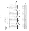
- FIG. 1A is a schematic view showing a state before an incidence of radiation. In this state, all lines of electric force run parallel inside a thick semiconductor film 51 . Where each split electrode 53 has a width “a” and a length “y” in the direction of depth, a sensitive area is “axy”.
- FIG. 1B is a schematic view showing a state occurring with an incidence of radiation. Of the charges (electrons and holes) generated in regions of space between the split electrodes 53 , the charges (e.g. holes in FIG. 1B ) moving toward the side having the split electrodes 53 are captured to stagnate (as at 55 ) adjacent surfaces of the thick semiconductor film 51 , in the absence of electrodes for sweeping out the holes.
- FIG. 2 shows a construction having an amorphous selenium (a-Se) film 65 and a common electrode 67 formed on a substrate 63 having a plurality of split electrodes 61 and thin film transistor (TFT) switches.
- the TFT switches are operable for successively reading signals.
- the amorphous selenium film has a thickness d.
- FIG. 2A which is a schematic view showing a state before an incidence of radiation, an electric potential adjacent the split electrodes 61 is sufficiently low. However, when an incidence of radiation takes place at a higher rate than the charge sweep-out, the charges collect adjacent the split electrodes 61 . This distorts the electric potential profile to raise the electric potential adjacent the split electrodes 61 as shown in FIG. 2B . Since a high bias must be applied to the amorphous selenium film in use, the potential rise becomes high enough to cause malfunctioning of the TFT switches. This results in phenomena such as of slow reading operation, and causes sensibility variations or after-outputs.
- This invention has been made having regard to the state of the art noted above, and its object is to provide a radiation detector having split electrodes and free from sensibility variations, which is achieved by stabilizing an electric field generated in the radiation detector by light irradiation.
- a radiation detector for detecting a spatial distribution of incident radiation comprising a radiation-sensitive semiconductor; a common electrode formed on one surface of the semiconductor for receiving a bias voltage; a plurality of split electrodes formed on the other surface of the semiconductor for outputting, as electric signals, charges generated within the semiconductor by the incident radiation; and a light irradiating mechanism for emitting light at least during a detection of the radiation.
- the radiation detector according to this invention has a light irradiating mechanism for emitting light to the split electrode side. This mechanism emits light during a radiation detecting operation.
- charges generated by the light i.e. holes where a positive bias is applied to the common electrode 9
- regions of space between the split electrodes 3 Consequently, lines of electric force are distorted, and each sensitive area is (a+b) ⁇ (y+z) from the beginning.
- FIG. 5 When an incidence of radiation takes place in this state, as shown in FIG. 5 , the charges moving toward the split electrodes 3 , of the charges generated in the regions of space between the split electrodes 3 , follow the lines of electric force to reach the split electrodes 3 .
- the light emission or irradiation herein includes all emission modes that produce the advantages of this invention, such as emitting light continuously or intermittently during a detection of the radiation.
- the light has a wavelength shorter than a wavelength corresponding to a band gap energy of the semiconductor used.
- the irradiating light Since the irradiating light has a wavelength shorter than a wavelength corresponding to the band gap energy of the semiconductor used, the irradiating light does not penetrate deep inside the semiconductor, but operates only in portions very close to the surface forming the split electrodes. The charges generated by the light collect only in limited regions very close to the surface forming the split electrodes, thereby reducing insensitive regions.
- the light has a wavelength shorter than a wavelength that halves a transmittance of the semiconductor used, and longer than a wavelength corresponding to a band gap energy of the semiconductor.
- the wavelength of the irradiating light is shorter than the wavelength that halves the transmittance and longer than the wavelength corresponding to the band gap energy of the semiconductor used, part of the irradiating light penetrates deep into the semiconductor to enlarge insensitive regions.
- the semiconductor is free from damage (generation of crystal defects) done by the irradiating light. No increase occurs in the dark current resulting from a charge detection by the irradiating light itself. Damaging of the semiconductor by the irradiating light is conspicuous with the amorphous semiconductor such as amorphous selenium (a-Se). This feature is effective particularly for the radiation detector using the amorphous semiconductor.
- a radiation detector for detecting a spatial distribution of incident radiation comprises a radiation-sensitive semiconductor; a common electrode formed on one surface of the semiconductor for receiving a bias voltage; a plurality of split electrodes formed on the other surface of the semiconductor for outputting, as electric signals, charges generated within the semiconductor by the incident radiation; a carrier selective intermediate layer formed at least between the semiconductor and the split electrodes; and a light irradiating mechanism for emitting light at least during a detection of the radiation.
- the radiation detector having an intermediate layer as noted above produces effects similar to those of the first aspect of the invention.
- the light has a wavelength shorter than a wavelength that halves the transmittance of the intermediate layer. It is more desirable that the light has a wavelength shorter than a wavelength that reduces the transmittance of the intermediate layer to 10%.
- the intermediate layer has more defects than the semiconductor layer and charges tend to collect in the intermediate layer, deflections of electric fields occur only in the intermediate layer.
- the emission of light from the side of split electrodes to the intermediate layer eliminates sensitivity variations and after-output due to the charges collected in the regions of the intermediate layer between the split electrodes.
- the light having a wavelength shorter than a wavelength that halves the transmittance of the intermediate layer a large part of the irradiating light is absorbed by the intermediate layer, thereby reducing the irradiating light reaching the semiconductor. This provides the effect of suppressing dark current in the semiconductor due to the irradiating light, besides suppressing dark current by means of the intermediate layer.
- the semiconductor comprises an amorphous material selected from non-dope selenium or non-dope selenium compound, selenium or selenium compound doped with As or Te, selenium doped with an alkali metal, a selenium compound doped an alkali metal, selenium doped with a halogen, a selenium compound doped with a halogen, and selenium or selenium compound doped with a combination of As, Te, an alkali metal and a halogen.
- an amorphous material selected from non-dope selenium or non-dope selenium compound, selenium or selenium compound doped with As or Te, selenium doped with an alkali metal, a halogen, a selenium compound doped with a halogen.
- the semiconductor comprises a polycrystalline material different from the intermediate layer and selected from compound semiconductors such as CdTe, CdZnTe, PbI2, HgI2, TlBr and GaAs, and the compound semiconductors doped with a halogen.
- compound semiconductors such as CdTe, CdZnTe, PbI2, HgI2, TlBr and GaAs, and the compound semiconductors doped with a halogen.
- the intermediate layer is provided in order to reduce dark current by using its carrier selectivity.
- the carrier selectivity is a property for remarkably differentiating the contribution to the charge transfer function between electrons and holes acting as charge transfer media (carriers) within the semiconductor.
- n-type semiconductors including, for example, polycrystals such as CeO 2 , CdS, CdSe, ZnSe and ZnS, and amorphous materials such as amorphous selenium doped with As or Te or alkali metals to lower the contribution of holes.
- Materials for increasing the contribution of holes are p-type semiconductors including polycrystals such as ZnTe, and amorphous materials such as amorphous selenium doped with halogen to lower the contribution of electrons.
- Sb 2 S 3 , CdTe, CdZnTe, PbI 2 and HgI2, TlBr, and non-dope amorphous selenium or selenium compound may increase the contribution of electrons or holes, depending on film-forming conditions.
- both the intermediate layer and semiconductor layer are formed of amorphous materials, the following combinations can be considered, for example.
- an amorphous material with a large contribution of holes is used for the intermediate layer adjacent the split electrodes. This inhibits entry of electrons from the split electrodes to reduce dark current.
- an intermediate layer with a large contribution of electrons may also be provided adjacent the common electrode. This will inhibit entry of holes from the common electrode, thereby further reducing dark current.
- an amorphous material with a large contribution of electrons is used for the intermediate layer adjacent the split electrodes. This inhibits entry of holes from the split electrodes to reduce dark current.
- an intermediate layer with a large contribution of holes may also be provided adjacent the common electrode. This will inhibit entry of electrons from the common electrode, thereby further reducing dark current.
- the semiconductor layer is an amorphous material and the intermediate layer a polycrystal, the following combinations are conceivable.
- an intermediate layer may also be provided adjacent the common electrode for further reducing dark current.
- an intermediate layer may also be provided adjacent the common electrode for further reducing dark current.
- the intermediate layer is formed on the surface of the semiconductor having the split electrodes, by using a material having a threshold wavelength of transmittance between a wavelength that halves a transmittance and a wavelength corresponding to a band gap energy of the semiconductor.
- the intermediate layer formed on the surface of the semiconductor having the split electrodes by using a material having a threshold wavelength of transmittance between a wavelength that halves a transmittance and a wavelength corresponding to a band gap energy of the semiconductor, has a filtering effect to produce the above effects without limiting the wavelength of irradiating light.
- the split electrodes are transparent or translucent to the irradiating light.
- the split electrodes are transparent or translucent, the light irradiates not only the regions of space between the split electrodes, but also electrode forming regions. Even when an incidence of radiation takes place at a higher rate than a charge sweep-out so that the charges once collect adjacent the split electrodes, the energy of the irradiating light excites the charges immediately again to give kinetic energy thereto. Consequently, the electric potential profile is not distorted, and no increase occurs with the potential adjacent the split electrodes. Thus, even with the a-Se film requiring application of a high bias voltage in use, the TFT switches can maintain a normal operation.
- FIG. 1 shows schematic views illustrating a first problem of a conventional radiation detector, in which FIG. 1A shows a state before an incidence of radiation, and FIG. 1B shows a state during an incidence of radiation;
- FIG. 2 shows schematic views illustrating a second problem of a conventional radiation detector, in which FIG. 2A shows a state before an incidence of radiation, and FIG. 2B shows a state during an incidence of radiation;
- FIG. 3 is a view in vertical section showing an outline of a radiation detector according to this invention.
- FIG. 4 is a schematic view showing a state before an incidence of radiation, for illustrating a first function of the radiation detector according to this invention
- FIG. 5 is a schematic view showing a state during an incidence of radiation, for illustrating the first function of the radiation detector according to this invention
- FIG. 6 is a schematic view showing a state during an irradiation with light having a wavelength shorter than a wavelength corresponding to a band gap, for illustrating the first function of the radiation detector according to this invention
- FIG. 7 is a view illustrating a second function of the radiation detector according to this invention.
- FIG. 8 is a timing chart showing an example of control of light irradiation during a detecting operation
- FIG. 9 is a timing chart showing another example of control of light irradiation during a detecting operation.
- FIG. 10 is a timing chart showing a further example of control of light irradiation during a detecting operation
- FIG. 11 is a view in vertical section showing an outline of an X-ray detector which is a modification of the embodiment according to this invention.
- FIG. 12 is an explanatory view showing that an intermediate layer has more defects than a thick semiconductor film, and tends to collect charges therein;
- FIG. 13 is a partly enlarged view in vertical section showing an example of light guide plate
- FIG. 14 is a graph showing transmittances of a-Se and Sb 2 S 3 thin films
- FIG. 15 is a graph showing, in enlargement, a rise portion of response characteristics in time of irradiation with lights of various wavelengths
- FIG. 16 is a graph showing, in enlargement, a fall portion of the response characteristics in time of irradiation with the lights of various wavelengths;
- FIG. 17 is an explanatory view showing charges collecting in both the thick semiconductor film and intermediate layer
- FIG. 18 is a graph for comparing characteristics of a testing X-ray detector according to the invention.
- FIG. 19 is another graph for comparing characteristics of the testing X-ray detector according to the invention.
- FIG. 3 is a view in vertical section showing an outline of the radiation detector.
- FIG. 4 is a schematic view showing a state before an incidence of radiation, for illustrating a first function of the radiation detector.
- FIG. 5 is a schematic view showing a state during an incidence of radiation.
- FIG. 6 is a schematic view showing a state during an irradiation with light having a wavelength shorter than a wavelength corresponding to a band gap.
- FIG. 7 is a view illustrating a second function of the radiation detector.
- the radiation detector in this embodiment includes a TFT substrate 5 having thin film transistor (TFT) switches, charge storage capacitors and split electrodes 3 formed on a transparent insulating substrate such as a glass substrate.
- a thick semiconductor film 7 of amorphous selenium (a-Se) is formed on the TFT substrate 5 , and a common electrode 9 for voltage application is formed on the upper surface of the thick a-Se semiconductor film 7 .
- the TFT substrate 5 has a planar light emitting plate 11 attached by a transparent adhesive to the back surface thereof adjacent the split electrodes 3 .
- the light emitting plate 11 has a green light emitting diode mounted therein and having a peak emission wavelength in the order of 570 nm.
- this planar light emitting plate 11 can emit light uniformly through the TFT substrate 5 to the surface of the thick a-Se semiconductor film 7 adjacent the split electrodes 3 .
- the above TFT substrate 5 and adhesive may be transparent only at the wavelength of the light emitted from the light emitting plate 11 .
- the irradiation by the light emitting plate 11 is continued at least while charges are read as electric signals by a signal processing circuit 13 and a gate driver 15 .
- the light emitting plate 11 corresponds to the light irradiating mechanism of this invention.
- the invention according to claim 2 or 3 may be implemented by selecting an emission wavelength of the light emitting diode elements in the light emitting plate 11 .
- a transmittance halving wavelength is 740 nm and a wavelength corresponding to 2.2 eV band gap energy is 560 nm.
- a blue light emitting diode having a peak emission wavelength in the order of 450 nm may be used to emit light of a wavelength shorter than the wavelength corresponding to the 2.2 eV band gap energy.
- the irradiating light does not penetrate deep inside the semiconductor, but only reaches shallow positions (referenced dp in FIG. 6 ). Since action takes place only in portions very close to the surface forming the split electrodes 3 , the charges generated by the light collect only in limited regions very close to the surface forming the split electrodes 3 , thereby reducing insensitive regions.
- the above planar light emitting plate 11 may be replaced with a cold cathode tube ( 25 ) and a phosphor as described hereinafter.
- light may be emitted with a wavelength shorter than the transmittance halving wavelength, and longer than the wavelength corresponding to the band gap energy.
- the wavelength of the irradiating light is shorter than the transmittance halving wavelength and longer than the wavelength corresponding to the band gap energy of the semiconductor used, part of the irradiating light penetrates deep into the semiconductor to enlarge insensitive regions.
- the semiconductor is free from damage (generation of crystal defects) done by the irradiating light. No increase occurs in the dark current resulting from a charge detection by the irradiating light itself. Damaging of the semiconductor by the irradiating light is conspicuous with the amorphous semiconductor such as amorphous selenium (a-Se).
- the construction set forth in claim 3 is effective particularly for the radiation detector using the amorphous semiconductor.
- the split electrodes 3 are in the form of transparent or translucent electrodes such as ITO, the light irradiates not only the regions of space between the split electrodes 3 , but also electrode forming regions (upper regions) through the split electrodes 3 . Even when an incidence of radiation takes place at a higher rate than a charge sweep-out so that the charges once collect adjacent the split electrodes 3 , as shown in FIG. 7 , the energy of the irradiating light excites the charges immediately again to give kinetic energy thereto. Consequently, the electric potential profile is not distorted, and no increase occurs with the potential adjacent the split electrodes. Thus, even with the a-Se film requiring application of a high bias voltage in use, the TFT switches 8 can maintain a normal operation.
- the split electrode 3 may be transparent only to the wavelength of the irradiating light.
- Amorphous materials include non-dope selenium or non-dope selenium compound, selenium or selenium compound doped with As or Te, selenium doped with an alkali metal such as Na, K or Li, a selenium compound doped an alkali metal, selenium doped with a halogen such as F or Cl, a selenium compound doped with a halogen such as F or Cl, and selenium or selenium compound doped with a combination of As, Te, an alkali metal such as Na, K or Li and a halogen such as F or Cl.
- the above materials doped with impurities have an advantage of excellent transport characteristics such as carrier mobility. Further, the amorphous materials may be prevented from crystallizing at high temperatures to realize an enhanced resistance to environment.
- Polycrystalline materials include compound semiconductors such as CdTe, CdZnTe, PbI 2 , HgI 2 , TlBr and GaAs, and the above compound semiconductors doped with a halogen such as F or Cl.
- the radiation detector may include an on/off switch 16 A operable by a photographer or the like, and a power source 16 B operable on an instruction from the on/off switch 16 A to supply electric power to the planar light emitting plate 11 for emitting light.
- a manual operation may be performed to emit light continuously or intermittently.
- the radiation detector may include a control unit 16 C for automatically controlling light emission by operating an on/off switch (not shown) mounted in the power source 16 B.
- a shutter film may be operated for mechanically cutting off irradiating light, for example.
- FIGS. 8 through 10 are timing charts showing examples of control of light irradiation during a detecting operation
- FIG. 8 refers.
- control unit 16 C While the control unit 16 C performs a detecting operation through the signal processing circuit 13 , radiation is emitted for two periods T 1 and T 2 in the meantime.
- the control unit 16 C operates the on/off switch in the power source 16 B to emit light continuously or intermittently. Particularly where light is emitted intermittently in a pulse shorter than a responsiveness of charge variations, an increase in dark current components by the light may be inhibited without spoiling the effect of charge collecting.
- FIG. 9 refers.
- the control unit 16 C emits radiation for two periods T 1 and T 2 during a detecting operation through the signal processing circuit 13 .
- the control unit 16 C turns on the on/off switch in the power source 16 B only for periods T 4 and T 5 corresponding to the radiation emitting periods T 1 and T 2 during the detecting operation.
- FIG. 10 refers.
- the control unit 16 C emits radiation for two periods T 1 and T 2 during a detecting operation through the signal processing circuit 13 .
- the control unit 16 C turns on the on/off switch in the power source 16 B only for periods T 6 and T 7 immediately following the radiation emitting periods T 1 and T 2 during the detecting operation.
- a control is made to emit light immediately after an incidence of radiation and until start of a next incidence.
- sensibility variations cannot be reduced but after-output can be reduced. Further, this control can inhibit an increase in dark current components by the light during the incidences of radiation.
- FIG. 11 is a view in vertical section showing an outline of an X-ray detector serving as the modification.
- this X-ray detector includes a TFT substrate 5 having thin film transistor (TFT) switches 17 , charge storage capacitors 19 and split electrodes 3 formed on a transparent insulating substrate such as a glass substrate.
- An intermediate layer 21 which is a thin film of antimony trisulfide (Sb 2 S 3 ) with a thickness of 1 ⁇ m, is formed on the TFT substrate 5 .
- a thick semiconductor film 7 of amorphous selenium (a-Se) is formed on the intermediate layer 21 , and a common electrode 9 for voltage application is formed on the upper surface of the thick a-Se semiconductor film 7 .
- the intermediate layer 21 herein has carrier selectivity, and has an effect of inhibiting dark current.
- the carrier selectivity is a property for remarkably differentiating the contribution to the charge transfer function between electrons and holes acting as charge transfer media (carriers) within the semiconductor.
- n-type semiconductors including, for example, polycrystals such as CeO 2 , CdS, CdSe, ZnSe and ZnS, alkali metals, and amorphous materials such as amorphous selenium doped with As or Te or alkali metals to lower the contribution of holes.
- p-type semiconductors including polycrystals such as ZnTe, and amorphous materials such as amorphous selenium doped with halogen to lower the contribution of electrons.
- Sb 2 S 3 , CdTe, CdZnTe, PbI 2 and HgI 2 , TlBr, and non-dope amorphous selenium or selenium compound may increase the contribution of electrons or holes, depending on film-forming conditions.
- the TFT substrate 5 has a light guide plate 23 attached by a transparent adhesive to the back surface thereof adjacent the split electrodes 3 .
- the light guide plate 23 is in the form of an acrylic plate having micromachined surfaces.
- a cold cathode tube 25 is attached to an end surface of the light guide plate 23 to act as a white light source.
- the light guide plate 23 and cold cathode tube 25 which correspond to the light irradiating mechanism and planar light emitting means of this invention, can, during a radiation detecting operation, emit light uniformly through the TFT substrate 5 to the surface of a-Se thick semiconductor film 7 adjacent the split electrodes 3 where the intermediate layer 21 is formed.
- the cold cathode tube 25 corresponds also to the linear light emitting means of this invention.
- the intermediate layer 21 has more defects than the thick semiconductor film 7 and charges A tend to collect in the intermediate layer 21 , deflections of electric fields occur only in the intermediate layer 21 .
- the intermediate layer 21 is provided adjacent the split electrodes 3 , the emission of light from the side of split electrodes 3 to the intermediate layer 21 eliminates sensitivity variations and after-output due to the charges collected in the regions of the intermediate layer 21 between the split electrodes 3 .
- An indirect light emitting device may be formed by combining the above cold cathode tube 25 and a phosphor that emits light of a preferred particular wavelength as described hereinafter.
- the cold cathode tube 25 field emission tube
- the gas discharge tube may be a plasma display panel (PDP) or field emission display panel (FEDP), for example.
- FIG. 13 is a partly enlarged view in vertical section showing an example of construction of the light guide plate.
- the light guide plate 23 includes, for example, a transparent plate 23 a having micromachined surfaces, a light diffusing sheet 23 b and a light reflecting sheet 23 c .
- the light diffusing sheet 23 b is applied to the surface of transparent plate 23 a opposed to the split electrodes 3
- the light reflecting sheet 23 c is applied to the other surface of transparent plate 23 a .
- the transparent plate 23 a may be a glass plate or acrylic plate, for example.
- the light reflecting sheet 23 c reflects the light from the light source to the transparent plate 23 a to promote use efficiency of the light.
- the light diffusing sheet 23 b diffuses the light to uniform the light emission.
- a large part of irradiating light may be emitted only to the intermediate layer 21 by using a wavelength shorter than a wavelength that halves the transmittance of the intermediate layer 21 .
- the light may be directed more concentratedly to the intermediate layer 21 by using a wavelength shorter than a wavelength that reduces the transmittance of the intermediate layer 21 to 10%.
- the light may be prevented from reaching the thick semiconductor film 7 . This eliminates adverse influences of an increase in dark current in the thick semiconductor film 7 due to the light irradiation.
- the wavelength that reduces the transmittance of the intermediate layer 21 to 10% is a wavelength of about 710 nm as seen from FIG. 14 , where amorphous selenium. (a-Se) is used as the intermediate layer 21 .
- This wavelength is about 660 nm where antimony trisulfide (Sb 2 S 3 ) film is used as the intermediate layer 21 .
- FIG. 15 is a graph showing, in enlargement, a rise portion of response characteristics in time of irradiation with lights of various wavelengths.
- FIG. 16 is a graph showing, in enlargement, a fall portion of the response characteristics in time of irradiation with the lights of various wavelengths.
- the red light shows low effects of reducing sensitivity variations and residual charges.
- infrared light referenced IR in the drawings
- a side effect of causing sensitivity to fall off at a rise time appears.
- a light of a long wavelength transmitted through the intermediate layer 21 not only fails to improve the situation but even has adverse influences.
- the intermediate layer 21 is formed of antimony trisulfide (Sb 2 S 3 ) at least, it is preferable to emit light of a wavelength shorter than 740 nm which is a transmittance halving wavelength.
- the blue light (referenced B in the drawings) and green light (referenced G in the drawings) with shorter wavelengths than the red light show outstanding effects of reducing sensitivity variations and residual charges.
- a light of short wavelength not transmitted through the intermediate layer 21 is preferable.
- the radiation detector in this embodiment and its modification apply a bias voltage to the common electrode 9 , and operate while the irradiating light is emitted.
- Charges (electrons and holes) generated in the thick semiconductor film 7 by incident radiation move toward the opposite electrodes.
- Charges induced by the movement of the charges (electrons and holes) are once stored in the charge storage capacitors 19 on the TFT substrate 5 connected through the split electrodes 3 .
- a gate driver 15 sends ON signals to turn on (connect) the thin film transistor (TFT) switches 17 . Then, the stored charges are successively outputted as radiation detection signals to the signal processing circuit 13 connected to the outside, thereby obtaining a two-dimensional image of the radiation.
- Amorphous materials include non-dope selenium or non-dope selenium compound, selenium or selenium compound doped with As or Te, selenium doped with an alkali metal such as Na, K or Li, selenium compound doped with an alkali metal, selenium doped with a halogen such as F or Cl, selenium compound doped with a halogen such as F or Cl, and selenium or selenium compound doped with a combination of an alkali metal such as As, Te, Na, K or Li, and a halogen such as F or Cl.
- the thick semiconductor film 7 should be formed of a material different from a material for the intermediate layer 21 .
- the intermediate layer 21 should be formed of a material different from a material for the thick semiconductor film 7 .
- both the intermediate layer 21 and thick semiconductor film 7 are formed of amorphous materials, the following combinations can be considered, for example.
- an amorphous material with a large contribution of holes is used for the intermediate layer 21 adjacent the split electrodes 3 . This inhibits entry of electrons from the split electrodes 3 to reduce dark current.
- an intermediate layer 21 with a large contribution of electrons may also be provided adjacent the common electrode 9 . This will inhibit entry of holes from the common electrode 9 , thereby further reducing dark current.
- an amorphous material with a large contribution of electrons is used for the intermediate layer 21 adjacent the split electrodes 3 . This inhibits entry of holes from the split electrodes 3 to reduce dark current.
- an intermediate layer 21 with a large contribution of holes may also be provided adjacent the common electrode 9 . This will inhibit entry of electrons from the common electrode 9 , thereby further reducing dark current.
- the thick semiconductor film 7 is an amorphous material and the intermediate layer 21 a polycrystal, the following combinations are conceivable.
- an intermediate layer 21 may also be provided adjacent the common electrode 9 for further reducing dark current.
- an intermediate layer 21 may also be provided adjacent the common electrode 9 for further reducing dark current.
- Polycrystalline materials suited for the intermediate layer 21 include compound semiconductors of Sb 2 S 3 , CeO 2 , CdS, CdSe, CdTe, CdZnTe, ZnSe, ZnTe, ZnS, PbI 2 , HgI 2 , TlBr and GaAs, these compound semiconductors doped with a halogen such as F or Cl, and a combination of these polycrystals forming multiple layers.
- the indirect light emitting device may be replaced with a direct light emitting device for directly emitting light of a particular wavelength.
- a direct light emitting device may be a light emitting diode, laser diode (LD) or electroluminescent device (EL).
- the above direct light emitting device may be arranged linearly to act as a linear light emitter, or may be arranged in a plane for use as the planer light emitting means of this invention. Furthermore, these direct light emitting devices may be formed directly on the TFT substrate 5 by double-sided device technique. This will realize a thin and compact mechanism relating to light irradiation.
- the intermediate layer 21 is provided, as shown in the schematic view of FIG. 17 , charges may collect in both the thick semiconductor film 7 and intermediate layer 21 . It is therefore necessary to emit light to both.
- the transmittance halving wavelength is 740 nm
- the wavelength corresponding to band gap energy 2.2 eV is 560 nm.
- the intermediate layer 21 may be formed by using a material having a threshold wavelength of transmittance of 560 nm to 740 nm.
- FIG. 14 is a graph showing transmittances of a-Se and Sb 2 S 3 films.
- the transmittance threshold wavelength of antimony trisulfide (Sb 2 S 3 ) film with a thickness of 1 ⁇ m is 580 nm
- the antimony trisulfide (Sb 2 S 3 ) film with a thickness of 1 ⁇ m may be formed between amorphous selenium and the split electrodes 3 . Then, the short wavelength components of 580 nm or less of the white light emerging from the cold cathode tube 25 are cut, whereby the energy of irradiating light becomes smaller than the band gap energy to avoid damage to the semiconductor by the irradiating light and an increase in dark current. It is necessary to select a material and thickness of the intermediate layer 21 according to the material used for the thick semiconductor film 7 .
- the radiation detector is free from sensitivity variations without causing damage due to irradiation and an increase in dark current.
- the intermediate layer 21 may be disposed directly under the common electrode 9 instead of being directly over the split electrodes 3 as in the foregoing example.
- the effects similar to those of the above construction may be produced by forming intermediate layers 21 directly under the common electrode 9 as well as directly over the split electrodes 3 . In this case, the two intermediate layers 21 need not be formed of the same material.
- a testing detector was fabricated as follows.
- the a-Se semiconductor layer 7 was formed with a thickness of 1 mm on the intermediate layer 21 , and then the common electrode 9 of Au film was formed with a thickness of 0.1 ⁇ m.
- a planar green light emitting diode is attached to the back surface of the TFT substrate 5 by a transparent adhesive.
- FIG. 18 shows output variations in time of emitting X-rays from an X-ray tube to the testing detector for four seconds with conditions of 55 kV tube voltage, 25 mA tube current, and 1 m distance. It will be seen that, when the light emitting diode emits no light, the detector is slow in response, and its output increases gradually, that is its sensitivity varies. When the light emitting diode emits light, the output rises almost instantly and remains constant during the X-ray irradiation. In time of non-emission from the light emitting diode, the output fails to exhibit a sharp stop upon cessation of the X-ray radiation, with a residual output continuing for one second or more.
- FIG. 19 shows output variations in time of emitting X-rays in an increased dose from the X-ray tube with the same 55 kV tube voltage and the tube current raised to a range of 50 mA to 80 mA.
- the detector shows a still slower response, and its output varies far in excess of the value accounted for by the electrode size and electrode intervals.
- peculiar residual curves appear after cessation of the X-ray radiation, which suggests malfunctioning of the TFT switches 17 .
- this phenomenon does not occur when the light emitting diode emits light.
- the output rises almost instantly and remains constant during the X-ray irradiation. Almost no residual output occurs after cessation of the X-ray irradiation.
- the light irradiating mechanism is attached to a lower position of the radiation detector. Where the split electrodes 3 of the radiation detector are located in an upper position, the light irradiating mechanism may be attached to the upper position of the radiation detector.
- the light irradiating mechanism in this invention may comprise a combination of a planer light emitting plate or a cold cathode tube and a power source, a combination of a cold cathode tube, a phosphor and a power source, a combination of these and a manual switch, a combination of these and a control unit, or in any other form that emits light.
Landscapes
- Physics & Mathematics (AREA)
- Health & Medical Sciences (AREA)
- Life Sciences & Earth Sciences (AREA)
- General Physics & Mathematics (AREA)
- High Energy & Nuclear Physics (AREA)
- Molecular Biology (AREA)
- Spectroscopy & Molecular Physics (AREA)
- Measurement Of Radiation (AREA)
- Light Receiving Elements (AREA)
- Solid State Image Pick-Up Elements (AREA)
Priority Applications (1)
| Application Number | Priority Date | Filing Date | Title |
|---|---|---|---|
| US11/241,931 US7034312B2 (en) | 2002-08-30 | 2005-10-04 | Radiation detector |
Applications Claiming Priority (4)
| Application Number | Priority Date | Filing Date | Title |
|---|---|---|---|
| JPJP2002-253819 | 2002-08-30 | ||
| JP2002253819 | 2002-08-30 | ||
| JPJP2003-57487 | 2003-03-05 | ||
| JP2003058487A JP4211435B2 (ja) | 2002-08-30 | 2003-03-05 | 放射線検出器 |
Related Child Applications (1)
| Application Number | Title | Priority Date | Filing Date |
|---|---|---|---|
| US11/241,931 Continuation US7034312B2 (en) | 2002-08-30 | 2005-10-04 | Radiation detector |
Publications (2)
| Publication Number | Publication Date |
|---|---|
| US20040079891A1 US20040079891A1 (en) | 2004-04-29 |
| US6995375B2 true US6995375B2 (en) | 2006-02-07 |
Family
ID=31497700
Family Applications (2)
| Application Number | Title | Priority Date | Filing Date |
|---|---|---|---|
| US10/629,676 Expired - Fee Related US6995375B2 (en) | 2002-08-30 | 2003-07-30 | Split-electrode radiation detector free of sensibility variations and after-outputs |
| US11/241,931 Expired - Fee Related US7034312B2 (en) | 2002-08-30 | 2005-10-04 | Radiation detector |
Family Applications After (1)
| Application Number | Title | Priority Date | Filing Date |
|---|---|---|---|
| US11/241,931 Expired - Fee Related US7034312B2 (en) | 2002-08-30 | 2005-10-04 | Radiation detector |
Country Status (7)
| Country | Link |
|---|---|
| US (2) | US6995375B2 (fr) |
| EP (1) | EP1394567B1 (fr) |
| JP (1) | JP4211435B2 (fr) |
| KR (1) | KR100582097B1 (fr) |
| CN (1) | CN1270390C (fr) |
| CA (1) | CA2438777A1 (fr) |
| DE (1) | DE60330633D1 (fr) |
Cited By (5)
| Publication number | Priority date | Publication date | Assignee | Title |
|---|---|---|---|---|
| US20050056829A1 (en) * | 2003-09-17 | 2005-03-17 | Green Michael C. | Reducing dark current of photoconductor using heterojunction that maintains high x-ray sensitivity |
| US20080203310A1 (en) * | 2007-01-19 | 2008-08-28 | Fujifilm Corporation | Radiation image detector |
| US20090159821A1 (en) * | 2007-12-21 | 2009-06-25 | Fujifilm Corporation | Radiation image detecting apparatus |
| US20090289170A1 (en) * | 2005-12-20 | 2009-11-26 | Canon Kabushiki Kaisha | Radiation detection apparatus and radiation detection system |
| US20120001201A1 (en) * | 2007-12-28 | 2012-01-05 | Fujifilm Corporation | Radiation image detection apparatus and manufacturing method of radiation image detector |
Families Citing this family (42)
| Publication number | Priority date | Publication date | Assignee | Title |
|---|---|---|---|---|
| JP3757946B2 (ja) * | 2003-03-18 | 2006-03-22 | 株式会社島津製作所 | 放射線撮像装置 |
| JP4269859B2 (ja) * | 2003-09-10 | 2009-05-27 | 株式会社島津製作所 | 放射線検出器 |
| CN102136502B (zh) * | 2004-03-31 | 2014-10-22 | 奥斯兰姆奥普托半导体有限责任公司 | 辐射探测器 |
| JP4254602B2 (ja) * | 2004-04-19 | 2009-04-15 | 株式会社島津製作所 | 二次元放射線検出器 |
| CN101048674A (zh) * | 2004-10-29 | 2007-10-03 | 株式会社岛津制作所 | 放射线检测器 |
| US7122803B2 (en) * | 2005-02-16 | 2006-10-17 | Hologic, Inc. | Amorphous selenium flat panel x-ray imager for tomosynthesis and static imaging |
| JP4622670B2 (ja) * | 2005-05-17 | 2011-02-02 | 株式会社島津製作所 | 2次元放射線検出器 |
| TW200712684A (en) * | 2005-09-30 | 2007-04-01 | Innolux Display Corp | Liquid crystal display module |
| US7795592B2 (en) | 2005-11-21 | 2010-09-14 | Fujifilm Corporation | Image detector and manufacturing method of the same |
| JP4762692B2 (ja) * | 2005-11-21 | 2011-08-31 | 富士フイルム株式会社 | 放射線画像検出器および放射線画像検出器の製造方法 |
| JP4834518B2 (ja) * | 2005-11-29 | 2011-12-14 | キヤノン株式会社 | 放射線撮像装置、その制御方法、及びそれを実行させるためのプログラムを記録した記録媒体 |
| JP5196739B2 (ja) * | 2006-06-09 | 2013-05-15 | キヤノン株式会社 | 放射線撮像装置及び放射線撮像システム |
| JP4992358B2 (ja) * | 2006-09-14 | 2012-08-08 | 株式会社島津製作所 | 電磁波検出器およびこれを用いた放射線撮影装置 |
| JP5049739B2 (ja) * | 2006-11-01 | 2012-10-17 | キヤノン株式会社 | 放射線撮像装置 |
| US7652258B2 (en) | 2007-01-08 | 2010-01-26 | Orbotech Medical Solutions Ltd. | Method, apparatus, and system of reducing polarization in radiation detectors |
| JP5455312B2 (ja) * | 2007-03-13 | 2014-03-26 | キヤノン株式会社 | 放射線撮像装置、その制御方法、及びプログラム |
| JP2008227346A (ja) * | 2007-03-15 | 2008-09-25 | Fujifilm Corp | 放射線検出装置 |
| JP2008244412A (ja) * | 2007-03-29 | 2008-10-09 | Fujifilm Corp | 放射線検出装置 |
| JP4862767B2 (ja) * | 2007-07-04 | 2012-01-25 | 株式会社島津製作所 | X線診断装置 |
| JP5007632B2 (ja) * | 2007-09-04 | 2012-08-22 | 株式会社島津製作所 | 放射線撮像装置 |
| US20100290047A1 (en) * | 2007-09-20 | 2010-11-18 | Novatrans Group Sa | Image Sensor Device and Method |
| CN101688919B (zh) * | 2007-10-23 | 2012-10-17 | 株式会社岛津制作所 | 光或放射线检测器及其制造方法 |
| KR20090102185A (ko) * | 2008-03-25 | 2009-09-30 | 삼성전자주식회사 | 엑스레이 검출기의 구동방법 및 이를 이용한 엑스레이검출기 |
| JP5197265B2 (ja) * | 2008-09-22 | 2013-05-15 | 富士フイルム株式会社 | 放射線撮影装置 |
| JP5377081B2 (ja) * | 2009-06-01 | 2013-12-25 | キヤノン株式会社 | 放射線撮影装置及びその制御方法 |
| KR101164653B1 (ko) | 2010-09-30 | 2012-07-11 | 주식회사 디알텍 | 방사선 검출기 및 방사선 검출 방법 |
| DE102012213494A1 (de) * | 2012-07-31 | 2014-02-06 | Siemens Aktiengesellschaft | Detektion von Röntgenstrahlung und Röntgendetektorsystem |
| DE102012213409B3 (de) * | 2012-07-31 | 2014-11-13 | Siemens Aktiengesellschaft | Röntgenstrahlungsdetektor, CT-System und Verfahren hierzu |
| DE102012213411B4 (de) | 2012-07-31 | 2018-11-29 | Siemens Healthcare Gmbh | Verfahren zur Detektion von Röntgenstrahlung |
| US9261609B2 (en) * | 2012-08-20 | 2016-02-16 | General Electric Company | Apparatus and methods for charge collection control in radiation detectors |
| JP6310471B2 (ja) * | 2012-11-09 | 2018-04-11 | コーニンクレッカ フィリップス エヌ ヴェKoninklijke Philips N.V. | 検出器結晶のためのサブバンド赤外照射 |
| JP6388608B2 (ja) * | 2013-03-01 | 2018-09-12 | コーニンクレッカ フィリップス エヌ ヴェKoninklijke Philips N.V. | 検出器、検出方法、投影データ生成システム、投影データ生成方法及びコンピュータプログラム |
| CN104218045A (zh) * | 2013-06-05 | 2014-12-17 | 朱兴华 | 碘化铅光电导层基数字x射线平板探测器 |
| JP2015181563A (ja) * | 2014-03-20 | 2015-10-22 | 株式会社島津製作所 | X線撮影装置 |
| US20150364052A1 (en) * | 2014-06-17 | 2015-12-17 | Stephen Brock Blankenship | Tactical injury simulating training device |
| CN107710021B (zh) * | 2015-07-09 | 2019-09-27 | 深圳帧观德芯科技有限公司 | 制作半导体x射线检测器的方法 |
| DE102015220793A1 (de) * | 2015-10-23 | 2017-04-27 | Siemens Healthcare Gmbh | Röntgendetektor und/oder Gammadetektor mit Lichtbias |
| DE102016210935B4 (de) * | 2016-06-20 | 2020-07-09 | Siemens Healthcare Gmbh | Röntgendetektor mit intransparenter Zwischenschicht |
| CN107153214B (zh) * | 2017-04-01 | 2019-06-07 | 西北核技术研究所 | 快时间响应半导体辐射探测器及其制作方法 |
| EP3422051A1 (fr) * | 2017-06-28 | 2019-01-02 | Koninklijke Philips N.V. | Détecteur de rayonnement à conversion directe |
| US10516068B1 (en) * | 2017-08-07 | 2019-12-24 | National Technology & Engineering Solutions Of Sandia, Llc | Thallium bromide (TIBr) semiconductors and devices with extended life apparatus, methods, and system |
| EP3852632B1 (fr) * | 2018-09-19 | 2024-08-07 | Shenzhen Xpectvision Technology Co., Ltd. | Détecteur de rayonnement à commande d'exposition automatique et procédé de commande d'exposition automatique |
Citations (7)
| Publication number | Priority date | Publication date | Assignee | Title |
|---|---|---|---|---|
| JPH099153A (ja) | 1995-06-07 | 1997-01-10 | E I Du Pont De Nemours & Co | 撮像パネルおよびその残留電荷を除去する方法 |
| JPH1085207A (ja) | 1996-08-05 | 1998-04-07 | Siemens Ag | X線診断装置 |
| US5937027A (en) | 1996-07-05 | 1999-08-10 | Commissariat A L'energie Atomique | Method and device for the taking of digital images with control and optimization of the exposure time of the object to X or γ radiation |
| US20010025938A1 (en) | 2000-03-22 | 2001-10-04 | Shinji Imai | Image storage medium and method of manufacturing the same |
| JP2002040144A (ja) | 2000-07-28 | 2002-02-06 | Canon Inc | 光電変換装置並びに光電変換デバイス、像情報処理システム及びその駆動方法 |
| WO2002034135A1 (fr) | 2000-10-25 | 2002-05-02 | Hitachi Medical Corporation | Dispositif de diagnostic a images radiologiques |
| US6600157B2 (en) * | 2000-06-27 | 2003-07-29 | Canon Kabushiki Kaisha | Semiconductor device, and radiation detection device and radiation detection system having same |
Family Cites Families (1)
| Publication number | Priority date | Publication date | Assignee | Title |
|---|---|---|---|---|
| US6194727B1 (en) * | 1998-07-06 | 2001-02-27 | Direct Radiography Corp. | Direct radiographic imaging panel having a dielectric layer with an adjusted time constant |
-
2003
- 2003-03-05 JP JP2003058487A patent/JP4211435B2/ja not_active Expired - Lifetime
- 2003-07-28 EP EP03017081A patent/EP1394567B1/fr not_active Expired - Lifetime
- 2003-07-28 DE DE60330633T patent/DE60330633D1/de not_active Expired - Lifetime
- 2003-07-30 US US10/629,676 patent/US6995375B2/en not_active Expired - Fee Related
- 2003-08-12 CN CNB031278566A patent/CN1270390C/zh not_active Expired - Fee Related
- 2003-08-26 KR KR1020030059010A patent/KR100582097B1/ko not_active IP Right Cessation
- 2003-08-29 CA CA002438777A patent/CA2438777A1/fr not_active Abandoned
-
2005
- 2005-10-04 US US11/241,931 patent/US7034312B2/en not_active Expired - Fee Related
Patent Citations (8)
| Publication number | Priority date | Publication date | Assignee | Title |
|---|---|---|---|---|
| JPH099153A (ja) | 1995-06-07 | 1997-01-10 | E I Du Pont De Nemours & Co | 撮像パネルおよびその残留電荷を除去する方法 |
| US5937027A (en) | 1996-07-05 | 1999-08-10 | Commissariat A L'energie Atomique | Method and device for the taking of digital images with control and optimization of the exposure time of the object to X or γ radiation |
| JPH1085207A (ja) | 1996-08-05 | 1998-04-07 | Siemens Ag | X線診断装置 |
| US20010025938A1 (en) | 2000-03-22 | 2001-10-04 | Shinji Imai | Image storage medium and method of manufacturing the same |
| US6600157B2 (en) * | 2000-06-27 | 2003-07-29 | Canon Kabushiki Kaisha | Semiconductor device, and radiation detection device and radiation detection system having same |
| JP2002040144A (ja) | 2000-07-28 | 2002-02-06 | Canon Inc | 光電変換装置並びに光電変換デバイス、像情報処理システム及びその駆動方法 |
| WO2002034135A1 (fr) | 2000-10-25 | 2002-05-02 | Hitachi Medical Corporation | Dispositif de diagnostic a images radiologiques |
| US20040022352A1 (en) | 2000-10-25 | 2004-02-05 | Katsumi Suzuki | X-ray image diagnosis apparatus |
Non-Patent Citations (1)
| Title |
|---|
| European Search Report, Application No.: 03017081.5-2213 PCT/, dated Jul. 20, 2005. |
Cited By (9)
| Publication number | Priority date | Publication date | Assignee | Title |
|---|---|---|---|---|
| US20050056829A1 (en) * | 2003-09-17 | 2005-03-17 | Green Michael C. | Reducing dark current of photoconductor using heterojunction that maintains high x-ray sensitivity |
| US20090289170A1 (en) * | 2005-12-20 | 2009-11-26 | Canon Kabushiki Kaisha | Radiation detection apparatus and radiation detection system |
| US7952058B2 (en) | 2005-12-20 | 2011-05-31 | Canon Kabushiki Kaisha | Radiation detection apparatus and radiation detection system having a light source located to reduce dark current |
| US20080203310A1 (en) * | 2007-01-19 | 2008-08-28 | Fujifilm Corporation | Radiation image detector |
| US7560700B2 (en) | 2007-01-19 | 2009-07-14 | Fujifilm Corporation | Radiation image detector |
| US20090159821A1 (en) * | 2007-12-21 | 2009-06-25 | Fujifilm Corporation | Radiation image detecting apparatus |
| US7652277B2 (en) | 2007-12-21 | 2010-01-26 | Fujifilm Corporation | Radiation image detecting apparatus |
| US20120001201A1 (en) * | 2007-12-28 | 2012-01-05 | Fujifilm Corporation | Radiation image detection apparatus and manufacturing method of radiation image detector |
| US8350207B2 (en) * | 2007-12-28 | 2013-01-08 | Fujifilm Corporation | Radiation image detection apparatus and manufacturing method of radiation image detector with substrate side charge transport layer |
Also Published As
| Publication number | Publication date |
|---|---|
| EP1394567A2 (fr) | 2004-03-03 |
| DE60330633D1 (de) | 2010-02-04 |
| CA2438777A1 (fr) | 2004-02-29 |
| EP1394567A3 (fr) | 2005-08-31 |
| JP4211435B2 (ja) | 2009-01-21 |
| KR100582097B1 (ko) | 2006-05-22 |
| CN1270390C (zh) | 2006-08-16 |
| US20040079891A1 (en) | 2004-04-29 |
| JP2004146769A (ja) | 2004-05-20 |
| EP1394567B1 (fr) | 2009-12-23 |
| CN1484321A (zh) | 2004-03-24 |
| US7034312B2 (en) | 2006-04-25 |
| US20060027757A1 (en) | 2006-02-09 |
| KR20040019930A (ko) | 2004-03-06 |
Similar Documents
| Publication | Publication Date | Title |
|---|---|---|
| US6995375B2 (en) | Split-electrode radiation detector free of sensibility variations and after-outputs | |
| JP3757946B2 (ja) | 放射線撮像装置 | |
| US7777167B2 (en) | Radiation imaging apparatus and radiation imaging system having a light source with light for calibration of conversion elements | |
| US5698858A (en) | Solid-state image intensifier and x-ray examination apparatus comprising a solid-state image intensifier | |
| US8530246B2 (en) | Method for controlling threshold voltage of semiconductor element | |
| JP2007155662A (ja) | 放射線検出装置及びそれを用いた放射線撮像システム | |
| US20060289769A1 (en) | Electromagnetic radiation detecting apparatus, radiation detecting apparatus, radiation detecting system and laser processing method | |
| KR102499097B1 (ko) | 전자기 방사선 검출 장치 | |
| JP2018085387A (ja) | 放射線検出器 | |
| US20100078559A1 (en) | Infra-red light stimulated high-flux semiconductor x-ray and gamma-ray radiation detector | |
| US6723995B2 (en) | Direct conversion flat panel X-ray detector with automatic cancellation of ghost images | |
| JP2007527987A (ja) | X線検出器素子 | |
| KR101711715B1 (ko) | X선 검출기 및 x선 측정 방법 | |
| US20100078558A1 (en) | Infra-red light stimulated cdZnTe spectroscopic semiconductor x-ray and gamma-ray radiation detector | |
| CN110070814B (zh) | Oled显示面板及其光衰减检测方法、显示装置 | |
| Risticj | The digital flat-panel x-ray detectors | |
| WO2017134896A1 (fr) | Procédé de fabrication de dispositif d'acquisition d'image radiographique | |
| JP2756463B2 (ja) | 赤外線イメージセンサ | |
| WO2012137425A1 (fr) | Détecteur de rayons x | |
| Scheuermann | Development of Avalanche Amorphous Selenium for X-Ray Detectors | |
| JPH11190774A (ja) | X線撮像装置 |
Legal Events
| Date | Code | Title | Description |
|---|---|---|---|
| AS | Assignment |
Owner name: SHIMADZU CORPORATION, JAPAN Free format text: ASSIGNMENT OF ASSIGNORS INTEREST;ASSIGNORS:SATO, KENJI;SATO, TOSHIYUKI;REEL/FRAME:014365/0648 Effective date: 20030630 |
|
| FEPP | Fee payment procedure |
Free format text: PAYOR NUMBER ASSIGNED (ORIGINAL EVENT CODE: ASPN); ENTITY STATUS OF PATENT OWNER: LARGE ENTITY |
|
| FPAY | Fee payment |
Year of fee payment: 4 |
|
| FPAY | Fee payment |
Year of fee payment: 8 |
|
| FEPP | Fee payment procedure |
Free format text: MAINTENANCE FEE REMINDER MAILED (ORIGINAL EVENT CODE: REM.) |
|
| LAPS | Lapse for failure to pay maintenance fees |
Free format text: PATENT EXPIRED FOR FAILURE TO PAY MAINTENANCE FEES (ORIGINAL EVENT CODE: EXP.) |
|
| STCH | Information on status: patent discontinuation |
Free format text: PATENT EXPIRED DUE TO NONPAYMENT OF MAINTENANCE FEES UNDER 37 CFR 1.362 |
|
| FP | Lapsed due to failure to pay maintenance fee |
Effective date: 20180207 |