US6987410B2 - Clock recovery circuit and communication device - Google Patents
Clock recovery circuit and communication device Download PDFInfo
- Publication number
- US6987410B2 US6987410B2 US10/835,253 US83525304A US6987410B2 US 6987410 B2 US6987410 B2 US 6987410B2 US 83525304 A US83525304 A US 83525304A US 6987410 B2 US6987410 B2 US 6987410B2
- Authority
- US
- United States
- Prior art keywords
- variable delay
- timing
- circuit
- clock signal
- plural stages
- Prior art date
- Legal status (The legal status is an assumption and is not a legal conclusion. Google has not performed a legal analysis and makes no representation as to the accuracy of the status listed.)
- Expired - Fee Related
Links
- 238000011084 recovery Methods 0.000 title claims abstract description 53
- 238000004891 communication Methods 0.000 title claims description 23
- 230000003111 delayed effect Effects 0.000 claims abstract description 90
- 238000005070 sampling Methods 0.000 claims abstract description 90
- 239000000872 buffer Substances 0.000 claims description 20
- 230000008859 change Effects 0.000 claims description 20
- 230000003071 parasitic effect Effects 0.000 claims description 5
- 238000012545 processing Methods 0.000 claims description 4
- 238000012360 testing method Methods 0.000 description 55
- 230000004044 response Effects 0.000 description 14
- 230000005540 biological transmission Effects 0.000 description 13
- 230000001934 delay Effects 0.000 description 13
- 230000007613 environmental effect Effects 0.000 description 6
- 238000000034 method Methods 0.000 description 6
- 230000008569 process Effects 0.000 description 6
- 230000001276 controlling effect Effects 0.000 description 4
- 238000001514 detection method Methods 0.000 description 4
- 101000693269 Homo sapiens Sphingosine 1-phosphate receptor 3 Proteins 0.000 description 3
- 102100025747 Sphingosine 1-phosphate receptor 3 Human genes 0.000 description 3
- 238000005259 measurement Methods 0.000 description 3
- 101001021281 Homo sapiens Protein HEXIM1 Proteins 0.000 description 2
- 101000693265 Homo sapiens Sphingosine 1-phosphate receptor 1 Proteins 0.000 description 2
- 102000004137 Lysophosphatidic Acid Receptors Human genes 0.000 description 2
- 108090000642 Lysophosphatidic Acid Receptors Proteins 0.000 description 2
- 102100025750 Sphingosine 1-phosphate receptor 1 Human genes 0.000 description 2
- 230000008901 benefit Effects 0.000 description 2
- 230000003247 decreasing effect Effects 0.000 description 2
- 238000003708 edge detection Methods 0.000 description 2
- 230000001419 dependent effect Effects 0.000 description 1
- 230000001915 proofreading effect Effects 0.000 description 1
- 230000001105 regulatory effect Effects 0.000 description 1
- 230000000630 rising effect Effects 0.000 description 1
- 238000006467 substitution reaction Methods 0.000 description 1
- YDLQKLWVKKFPII-UHFFFAOYSA-N timiperone Chemical compound C1=CC(F)=CC=C1C(=O)CCCN1CCC(N2C(NC3=CC=CC=C32)=S)CC1 YDLQKLWVKKFPII-UHFFFAOYSA-N 0.000 description 1
- 229950000809 timiperone Drugs 0.000 description 1
Images


Classifications
-
- H—ELECTRICITY
- H03—ELECTRONIC CIRCUITRY
- H03K—PULSE TECHNIQUE
- H03K5/00—Manipulating of pulses not covered by one of the other main groups of this subclass
- H03K5/01—Shaping pulses
-
- G—PHYSICS
- G01—MEASURING; TESTING
- G01R—MEASURING ELECTRIC VARIABLES; MEASURING MAGNETIC VARIABLES
- G01R31/00—Arrangements for testing electric properties; Arrangements for locating electric faults; Arrangements for electrical testing characterised by what is being tested not provided for elsewhere
- G01R31/28—Testing of electronic circuits, e.g. by signal tracer
- G01R31/317—Testing of digital circuits
- G01R31/3181—Functional testing
- G01R31/319—Tester hardware, i.e. output processing circuits
- G01R31/31917—Stimuli generation or application of test patterns to the device under test [DUT]
- G01R31/31922—Timing generation or clock distribution
-
- H—ELECTRICITY
- H03—ELECTRONIC CIRCUITRY
- H03K—PULSE TECHNIQUE
- H03K5/00—Manipulating of pulses not covered by one of the other main groups of this subclass
- H03K5/13—Arrangements having a single output and transforming input signals into pulses delivered at desired time intervals
- H03K5/135—Arrangements having a single output and transforming input signals into pulses delivered at desired time intervals by the use of time reference signals, e.g. clock signals
-
- H—ELECTRICITY
- H03—ELECTRONIC CIRCUITRY
- H03L—AUTOMATIC CONTROL, STARTING, SYNCHRONISATION OR STABILISATION OF GENERATORS OF ELECTRONIC OSCILLATIONS OR PULSES
- H03L7/00—Automatic control of frequency or phase; Synchronisation
- H03L7/06—Automatic control of frequency or phase; Synchronisation using a reference signal applied to a frequency- or phase-locked loop
- H03L7/08—Details of the phase-locked loop
- H03L7/0805—Details of the phase-locked loop the loop being adapted to provide an additional control signal for use outside the loop
-
- H—ELECTRICITY
- H03—ELECTRONIC CIRCUITRY
- H03L—AUTOMATIC CONTROL, STARTING, SYNCHRONISATION OR STABILISATION OF GENERATORS OF ELECTRONIC OSCILLATIONS OR PULSES
- H03L7/00—Automatic control of frequency or phase; Synchronisation
- H03L7/06—Automatic control of frequency or phase; Synchronisation using a reference signal applied to a frequency- or phase-locked loop
- H03L7/08—Details of the phase-locked loop
- H03L7/081—Details of the phase-locked loop provided with an additional controlled phase shifter
- H03L7/0812—Details of the phase-locked loop provided with an additional controlled phase shifter and where no voltage or current controlled oscillator is used
- H03L7/0816—Details of the phase-locked loop provided with an additional controlled phase shifter and where no voltage or current controlled oscillator is used the controlled phase shifter and the frequency- or phase-detection arrangement being connected to a common input
-
- H—ELECTRICITY
- H04—ELECTRIC COMMUNICATION TECHNIQUE
- H04L—TRANSMISSION OF DIGITAL INFORMATION, e.g. TELEGRAPHIC COMMUNICATION
- H04L1/00—Arrangements for detecting or preventing errors in the information received
- H04L1/20—Arrangements for detecting or preventing errors in the information received using signal quality detector
- H04L1/205—Arrangements for detecting or preventing errors in the information received using signal quality detector jitter monitoring
-
- H—ELECTRICITY
- H04—ELECTRIC COMMUNICATION TECHNIQUE
- H04L—TRANSMISSION OF DIGITAL INFORMATION, e.g. TELEGRAPHIC COMMUNICATION
- H04L1/00—Arrangements for detecting or preventing errors in the information received
- H04L1/24—Testing correct operation
-
- H—ELECTRICITY
- H04—ELECTRIC COMMUNICATION TECHNIQUE
- H04L—TRANSMISSION OF DIGITAL INFORMATION, e.g. TELEGRAPHIC COMMUNICATION
- H04L7/00—Arrangements for synchronising receiver with transmitter
- H04L7/0016—Arrangements for synchronising receiver with transmitter correction of synchronization errors
- H04L7/0033—Correction by delay
- H04L7/0037—Delay of clock signal
-
- H—ELECTRICITY
- H04—ELECTRIC COMMUNICATION TECHNIQUE
- H04L—TRANSMISSION OF DIGITAL INFORMATION, e.g. TELEGRAPHIC COMMUNICATION
- H04L7/00—Arrangements for synchronising receiver with transmitter
- H04L7/02—Speed or phase control by the received code signals, the signals containing no special synchronisation information
-
- H—ELECTRICITY
- H03—ELECTRONIC CIRCUITRY
- H03K—PULSE TECHNIQUE
- H03K5/00—Manipulating of pulses not covered by one of the other main groups of this subclass
- H03K2005/00013—Delay, i.e. output pulse is delayed after input pulse and pulse length of output pulse is dependent on pulse length of input pulse
- H03K2005/00019—Variable delay
- H03K2005/00026—Variable delay controlled by an analog electrical signal, e.g. obtained after conversion by a D/A converter
-
- H—ELECTRICITY
- H04—ELECTRIC COMMUNICATION TECHNIQUE
- H04L—TRANSMISSION OF DIGITAL INFORMATION, e.g. TELEGRAPHIC COMMUNICATION
- H04L7/00—Arrangements for synchronising receiver with transmitter
- H04L7/0008—Synchronisation information channels, e.g. clock distribution lines
-
- H—ELECTRICITY
- H04—ELECTRIC COMMUNICATION TECHNIQUE
- H04L—TRANSMISSION OF DIGITAL INFORMATION, e.g. TELEGRAPHIC COMMUNICATION
- H04L7/00—Arrangements for synchronising receiver with transmitter
- H04L7/0016—Arrangements for synchronising receiver with transmitter correction of synchronization errors
- H04L7/0033—Correction by delay
- H04L7/0041—Delay of data signal
Definitions
- the present invention relates to a clock recovery circuit and a communication device. More particularly, the present invention relates to a clock recovery circuit for adjusting the timing of a clock signal against a data signal and a communication device provided with the clock recovery circuit.
- a communication LSI employs a clock recovery circuit for adjusting the phase of a clock signal to retrieve a data signal.
- Such clock recovery circuit compares the phases of the data signal and the clock signal and adjusts the phase of the clock signal using a variable delay circuit.
- a conventional variable delay circuit is configured with a rough delay circuit whose resolution is low and variable amount is large, a fine delay circuit whose resolution is high and variable amount is the same as the rough delay circuit and a fine delay circuit for compensating the change of the propagation delay time due to the change of the noise or the environmental conditions in real time.
- VCO voltage controlled oscillator
- a clock recovery circuit for adjusting timing of a clock signal to a data signal includes plural stages of first variable delay elements coupled in series for sequentially delaying the data signal by a first delay amount, plural stages of second variable delay elements coupled in series for sequentially delaying the clock signal generated by a reference clock generating circuit as much as a second delay amount which is larger than the first delay amount, a plurality of timing comparators for sampling each of a plurality of the data signals delayed by each of the plural stages of first variable delay elements with the clock signal delayed by the second variable delay elements whose stages are respectively the same as the plural stages of first variable delay elements, a plurality of EOR circuits for performing exclusive OR operation respectively on sets of a plurality of the sampling results, a pair of sampling results by each of pairs of the sequential timing comparators being taken as one of the sets of a plurality of the sampling results, a timing judging unit for judging the timing of the clock signal generated by the reference clock generating circuit corresponding to the data signal based on an operation result of
- the timing judging unit may judge the timing of the clock signal generated by the reference clock generating circuit corresponding to the data signal by detecting timing of the clock signal as an edge of the data signal, when one of the timing comparators receiving the clock signal samples the pair of sampling results, the pair of sampling results being used by one of the plurality of EOR circuits performing exclusive OR operation, the one of the EOR circuits outputting a logic value which indicates that the pair of sampling results are different from each other.
- the plurality of timing comparators may include a first timing comparator group, which is a set of the plurality of timing comparators for sampling the data signal based on the clock signal, whose time delayed is a first delay time or less, and a second timing comparator group, which is a set of the plurality of the timing comparators for sampling the data signal based on the clock signal, whose time delayed is a second delay time or more
- the plurality of EOR circuits may include a first EOR circuit group which is a set of the plurality of EOR circuits using sampling results of the plurality of timing comparators for exclusive OR operation, the plurality of timing comparators being included by the first timing comparator group and a second EOR circuit group which is a set of the plurality of EOR circuits using sampling results of the plurality of timing comparators for exclusive OR operation, the plurality of timing comparators being included by the second timing comparator group
- the timing judging unit may include a first OR circuit for performing OR operation on operation results of the plurality of EOR circuits included by the
- the plurality of timing comparators may further include a third timing comparator group, which is a set of the plurality of timing comparators for sampling the data signal based on the clock signal, whose time delayed is larger than the first delay time and smaller than the second delay time
- the plurality of EOR circuits may further include a third EOR circuit group which is a set of the plurality of EOR circuits used for exclusive OR operation on sampling results of the plurality of timing comparators included by the third timing comparator group
- the timing judging unit may further include a third OR circuit for performing OR operation on operation results of the plurality of EOR circuits included by the third EOR circuit group
- the recovery variable delay circuit may not change a delay amount of the clock signal generated by the reference clock generating circuit, if the third OR circuit outputs a logical value “1”.
- the timing judging unit may further include a counter for counting a number of times each of the first and second OR circuits outputs the logic value “1”, if each of the plurality of timing comparators performs sampling operation a plurality of times on each of the plurality of data signals at timing of each of the plurality of clock signals, while each of the plurality of EOR circuits performs exclusive OR operation a plurality of times and each of the first and second OR circuits performs OR operation a plurality of times, and the recovery variable delay circuit may change a delay amount of the clock signal generated by the reference clock generating circuit based on a count value of the counter.
- the clock recovery circuit may further include plural stages of third variable delay elements coupled in series for sequentially delaying the clock signal generated by the reference clock generating circuit, the plural stages of third variable delay elements having substantially the same delay characteristics as the plural stages of first variable delay elements, a fourth variable delay element coupled in parallel to the plural stages of third variable delay elements for delaying the clock signal generated by the reference clock generating circuit, a phase comparator for comparing a phase of the clock signal delayed by the plural stages of third variable delay elements with a phase of the clock signal delayed by the fourth variable delay element, and a first delay amount control unit for controlling delay amounts of the plural stages of third variable delay elements and the plural stages of first variable delay elements based on a comparison result of the phase comparator in order that the phase of the clock signal delayed by the plural stages of third variable delay elements and the phase of the data signal delayed by the plural stages of first variable delay elements are substantially the same as a phase of the clock signal delayed by the fourth variable delay element after predetermined cycles.
- the clock recovery circuit may further include plural stages of fifth variable delay elements coupled in series for sequentially delaying the clock signal generated by the reference clock generating circuit, the plural stages of third variable delay elements having substantially the same delay characteristics as the plural stages of first variable delay elements, a sixth variable delay element coupled in parallel to the plural stages of fifth variable delay elements for delaying the clock signal generated by the reference clock generating circuit, a phase comparator for comparing a phase of the clock signal delayed by the plural stages of fifth variable delay elements and a phase of the clock signal delayed by the sixth variable delay element, and a second delay amount control unit for controlling delay amounts of the plural stages of fifth variable delay elements and the plural stages of second variable delay elements based on a comparison result of the phase comparator in order that the phase of the clock signal delayed by the plural stages of fifth variable delay elements and the phase of the data signal delayed by the plural stages of second variable delay elements are substantially the same as a phase of the clock signal delayed by the sixth variable delay element after predetermined cycles.
- Each of the plurality of timing comparators may include a dynamic D flip-flop circuit for latching and outputting the data signal received from the first variable delay circuit using parasitic capacitance thereof based on the clock signal received by the corresponding timing comparator, a buffer for delaying the clock signal received by the corresponding timing comparator as much as a predetermined time, and a D flip-flop circuit for latching and outputting an output signal outputted by the dynamic D flip-flop circuit based on the clock signal delayed by the buffer.
- a communication device for synchronously processing a data signal with a clock signal includes a reference clock generating circuit for generating the clock signal, a clock recovery circuit for adjusting timing of the clock signal to the data signal, and a reception terminal logic circuit for synchronously processing the data signal with the clock signal.
- the clock recovery circuit includes plural stages of first variable delay elements coupled in series for sequentially delaying the data signal by a first delay amount, plural stages of second variable delay elements coupled in series for sequentially delaying the clock signal generated by a reference clock generating circuit as much as a second delay amount which is larger than the first delay amount, a plurality of timing comparators for sampling each of a plurality of the data signals delayed by each of the plural stages of first variable delay elements with the clock signal delayed by the second variable delay elements whose stages are respectively the same as the plural stages of first variable delay elements, a plurality of EOR circuits for performing exclusive OR operation respectively on sets of a plurality of the sampling results, a pair of sampling results by each of pairs of the sequential timing comparators being taken as one of the sets of a plurality of the sampling results, a timing judging unit for judging the timing of the clock signal generated by the reference clock generating circuit corresponding to the data signal based on an operation result of each of the plurality of EOR circuits, and are covery variable delay circuit for delaying the clock signal
- FIG. 1 shows an example of the configuration of a timing comparator.
- FIG. 2 shows an example of the configuration of a dynamic D flip-flop circuit.
- FIG. 3 shows an example of the configuration of a positive feedback D flip-flop circuit.
- FIG. 4 shows an example of the configuration of a variable delay circuit.
- FIG. 5 shows an example of the configuration of a variable delay circuit.
- FIG. 6 shows an example of the configuration of a phase comparator.
- FIG. 7 shows an example of the configuration of a testing apparatus.
- FIG. 8 shows an example of the configuration of a comparing unit.
- FIG. 9 shows an example of the configuration of a testing apparatus.
- FIG. 10 shows an example of the configuration of a signal characteristic detecting unit.
- FIG. 11 shows an example of the phase detection operation by a signal characteristic detecting unit.
- FIG. 12 shows an example of the configuration of the signal characteristic detecting unit.
- FIG. 13 shows an example of the edge detection operation by the signal characteristic detecting unit.
- FIG. 14 shows an example of the configuration of the signal characteristic detecting unit.
- FIG. 15 shows an example of the jitter measurement operation by the signal characteristic detecting unit.
- FIG. 16 shows an example of the jitter measurement operation by the signal characteristic detecting unit.
- FIG. 17 shows an example of the configuration of communication devices.
- FIG. 18 shows an example of the configuration of a clock recovery circuit.
- FIG. 19 shows an example of the configuration of the clock recovery circuit.
- FIG. 1 shows an example of the configuration of a timing comparator 100 according to this invention.
- the timing comparator 100 includes a dynamic D flip-flop circuit 102 , a buffer 104 and a positive feedback D flip-flop circuit 106 , and samples and outputs a data signal (D) by a clock signal (CK).
- the dynamic D flip-flop circuit 102 latches and outputs the data signal (D) by its parasitic capacitance based on the clock signal (CK) received by the timing comparator 100 and supplies it to the positive feedback D flip-flop circuit 106 .
- the buffer 104 delays the clock signal (CK) received by the timing comparator 100 by a predetermined time and supplies it to the positive feedback D flip-flop circuit 106 .
- the positive feedback D flip-flop circuit 106 latches and outputs the output signal outputted by the dynamic D flip-flop circuit 102 based on the clock signal (CK) delayed by the buffer 104 using its positive feedback circuit.
- the buffer 104 preferably delays the clock signal (CK) more than the hold time of the positive feedback D flip-flop circuit 106 .
- the positive feedback D flip-flop circuit 106 is an example of the D flip-flop circuit of this invention.
- the timing comparator 100 includes the buffer 104 , whereby it can allow the dynamic D flip-flop circuit 102 and the positive feedback D flip-flop circuit 106 not to perform a pipeline process but to operate as a delay line. In other words, the dynamic D flip-flop circuit 102 and the positive feedback D flip-flop circuit 106 can operate with the same clock signal.
- FIG. 2 shows an example of the configuration of the dynamic D flip-flop circuit 102 .
- the dynamic D flip-flop circuit 102 includes a first analog switch 200 , a first inverter 202 , a second analog switch 204 , and a second inverter 206 .
- the first analog switch 200 performs an on/off control based on the clock signal (CK) received by the timing comparator 100 .
- the first inverter 202 inverts and outputs the signal passing through the first analog switch 200 .
- the second analog switch 204 is coupled to the next stage of the first inverter 202 and performs the on/off control inverse to the on/off control of the first analog switch 200 based on the clock signal (CK) received by the timing comparator 100 .
- the second inverter 206 inverts and outputs the signal passing through the second analog switch 204 .
- the first and second analog switches 200 and 204 are analog switches using P-channel/N-channel transistors and perform switching operation by CKP whose phase is the same as CK and CKN whose phase is inverse to it.
- the first and second inverters 202 and 206 are CMOS inverters.
- the dynamic D flip-flop circuit 102 configures a sample-and-hold circuit by the analog switches, the first and second analog switches 200 and 204 , and the parasitic capacitance such as the gate capacitance and the wiring capacitance of the first and second inverters 202 and 206 .
- the dynamic D flip-flop circuit 102 does not include a loop circuit, its logic output becomes an intermediate level between “H” and “L” levels unless the electric charge is sufficient.
- the phase width to output the intermediate level is extremely small, and the width of the hysteresis is extremely small.
- FIG. 3 shows an example of the configuration of the positive feedback D flip-flop circuit 106 .
- the positive feedback D flip-flop circuit 106 includes a third analog switch 300 , a third inverter 302 , a fourth analog switch 304 , a fourth inverter 306 , a fifth inverter 308 , a fifth analog switch 310 , a sixth inverter 312 , and a sixth analog switch 314 .
- the third analog switch 300 performs an on/off control based on the clock signal (CK) delayed by the buffer 104 .
- the third inverter 302 inverts and outputs the signal passing through the third analog switch 300 .
- the fourth analog switch 304 is coupled to the next stage of the third inverter 302 , and performs the on/off control inverse to the on/off control of the third analog switch 300 based on the clock signal (CK) delayed by the buffer 104 .
- the fourth inverter 306 inverts and outputs the signal passing through the fourth analog switch 304 .
- the fifth inverter 308 inverts and outputs the signal passing through the third analog switch 302 .
- the fifth analog switch 310 which is coupled to the next stage of the fifth inverter 308 , performs the on/off control inverse to the on/off control of the third analog switch 300 based on the clock signal (CK) delayed by the buffer 104 and supplies the passing signal to the third inverter 302 .
- the sixth inverter 312 inverts and outputs the signal passing through the fourth analog switch 306 .
- the sixth analog switch 314 which is coupled to the next stage of the sixth inverter 312 , performs the on/off control inverse to the on/off control of the fourth analog switch 304 based on the clock signal (CK) delayed by the buffer 104 and supplies the passing signal to the fourth inverter 306 .
- the third, fourth, fifth and sixth analog switches 300 , 304 , 310 and 314 are analog switches using P-channel/N-channel transistors and perform switching operation by CKP whose phase is the same as CK and CKN whose phase is inverse to it.
- the third, fourth, fifth and sixth inverters 302 , 306 , 308 and 312 are CMOS inverters.
- the positive feedback D flip-flop circuit 106 holds the output of the third analog switch 300 by the loop circuit which consists of the third and fifth inverters 302 and 308 and the fifth analog switch 310 , while holding the output of the fourth analog switch 304 which consists of the fourth and sixth inverters 306 and 312 and the sixth analog switch 314 .
- the positive feedback D flip-flop circuit 106 amplifies and outputs the signal by its positive feedback circuit. Accordingly, if the data signal (D) of an intermediate level is inputted from the dynamic D flip-flop circuit 102 , hysteresis occurs. However, the width of the hysteresis is such that the logic output of the dynamic D flip-flop circuit 102 becomes the intermediate level, so it is extremely small. Therefore, according to the timing comparator 100 related to this invention, the logic output of an intermediate level is not outputted, and thus the time required until the phase is locked can be reduced, so it is possible to correspond to a higher frequency band.
- FIG. 4 shows an example of the configuration of a variable delay circuit 400 according to this invention.
- the variable delay circuit 400 is a DLL (Delay Lock Loop) circuit and delays and outputs a reference clock signal by a designated time.
- the variable delay circuit 400 includes plural stages of variable delay elements 402 , a selector 403 , a variable delay element 404 , a phase comparator 406 , and a delay amount control unit 408 .
- the delay amount control unit 408 includes a counter 410 and a DAC 412 .
- the plural stages of variable delay elements 402 which are coupled in series sequentially delay the reference clock signal and supply it to the selector 403 .
- the selector 403 selects one reference clock signal among a plurality of reference clock signals or data signals outputted by the plural stages of variable delay elements 402 in a reciprocally independent manner and supplies it to the phase comparator 406 , while selecting one reference clock signal among a plurality of reference clock signals or data signals outputted by the plural stages of variable delay elements 402 and supplying it out of the variable delay circuit 400 .
- the variable delay element 404 which is coupled in parallel to the plural stages of variable delay elements 402 delays the reference clock signal.
- phase comparator 406 compares the phase of the reference clock signal delayed by the plural stages of variable delay elements 402 , supplied from the selector 403 , with the phase of the reference clock signal delayed by the variable delay element 404 .
- the delay amount control unit 408 controls the delay amount of each of the plural stages of variable delay elements 402 based on the comparison result of the phase comparator 406 in order that the phase of the reference clock signal delayed by the plural stages of variable delay elements 402 , supplied from the selector 403 , is approximately the same as the phase of the reference clock signal delayed by the variable delay element 404 for each of predetermined cycles.
- the phase comparator 406 outputs a flag signal that indicates whether the phase of the reference clock signal delayed by the plural stages of variable delay elements 402 is early or late relatively to the phase of the reference clock signal delayed by the variable delay element 404 .
- the counter 410 increases the count value if the flag signal outputted from the phase comparator 406 indicates that the phase of the reference clock signal delayed by the plural stages of variable delay elements 402 is early, whereas decreasing the count value if the flag signal indicates that it is late.
- the DAC 412 supplies a bias signal to control the delay amounts for the plural stages of variable delay elements 402 based on the count value of the counter 410 .
- variable delay circuit 400 since the variable amounts of the propagation delay time of the plural stages of variable delay elements 402 caused by the change of processes or the environmental change such as voltage or temperature can be assigned to the lock range of the DLL, each of the variable delay elements 402 has its variable amount as much as (the delay amount of the variable delay element 404 ))/(the number of the stages of the variable delay elements 402 used in the DLL), and thus it is possible to absorb the deviation of the propagation delay time of the plural stages of variable delay elements 402 caused by the change of processes or the environmental change such as voltage or temperature. Further, the width of the period of the reference clock signal which can be delayed can be increased, and even if the period of the reference clock signal changes, it is possible to easily correspond to such situation simply by the process of software without correcting any circuits.
- FIG. 5 shows an example of the configuration of a variable delay circuit 500 according to this invention.
- the variable delay circuit 500 includes a DLL circuit which is an example of the variable delay circuit 400 shown in FIG. 4 and delays the data signal by a predetermined time and outputs it.
- the variable delay circuit 500 includes plural stages of variable delay elements 502 and a selector 504 in addition to the configuration elements of the variable delay circuit 400 shown in FIG. 4 .
- the plural stages of variable delay elements 502 which have approximately the same delay characteristics as the plural stages of variable delay elements 402 are coupled in series and sequentially delay the data signal. By decreasing the number of the stages of the variable delay elements 402 to such a limit as the number of the stages required for the delay time as much as the period of the reference clock signal, the circuit size can be reduced. And the selector 504 selects one of the data signals outputted by the plural stages of variable delay elements 502 and outputs it out of the variable delay circuit 500 .
- the delay amount control unit 408 controls the delay amount of each of the plural stages of variable delay elements 402 based on the comparison result of the phase comparator 406 in order that the phase of the reference clock signal delayed by the plural stages of variable delay elements 402 is approximately equal to the phase of the reference clock signal delayed by the variable delay element 404 after predetermined cycles, while controlling the delay amount of each of the plural stages of variable delay elements 402 in order that the phase of the reference clock signal delayed by the plural stages of variable delay elements 502 is approximately equal to the phase of the reference clock signal delayed by the variable delay element 404 after predetermined cycles.
- the delay amount control unit 408 controls the delay amount by supplying a first control signal to each of the plural stages of variable delay elements 402 , whereas controlling the delay amount by supplying a second control signal uniquely determined from the first control signal to each of the plural stages of variable delay elements 502 .
- the delay amount control unit 408 may control the plural stages of variable delay elements 402 and the plural stages of variable delay elements 502 to have approximately the same delay amount by supplying the first control signal to each of the plural stages of variable delay elements 402 where as supplying the second control signal which is the same as the first control signal to each of the plural stages of variable delay elements 502 .
- FIG. 6 shows an example of the configuration of a phase comparator 406 .
- the phase comparator 406 includes a dynamic D flip-flop circuit 600 and a positive feedback D flip-flop circuit 602 .
- the dynamic D flip-flop circuit 600 latches and outputs the reference clock signal delayed by the plural stages of variable delay elements 402 by its parasitic capacitance based on the reference clock signal delayed by the variable delay element 404 .
- the positive feedback D flip-flop circuit 602 latches and outputs the output signal outputted by the dynamic D flip-flop circuit 600 by its positive feedback circuit based on the reference clock signal delayed by the variable delay element 404 .
- the dynamic D flip-flop circuit 600 has the same configuration and function as the dynamic D flip-flop circuit 102 shown in FIG. 2
- the positive feedback D flip-flop circuit 602 has the same configuration and function as the positive feedback D flip-flop circuit 106 shown in FIG. 3 , so they will not be described.
- FIG. 7 shows an example of the configuration of the testing apparatus 700 according to a first exemplary embodiment of this invention.
- the testing apparatus 700 includes a pattern generator 702 , a waveform formatting unit 704 , a timing generator 706 , a reference clock generator 708 , a timing generator 710 , a comparing unit 712 , and a judging unit 704 .
- the pattern generator 702 generates the data signal to be supplied to the device under test 716 and supplies it to the waveform formatting unit 704 .
- the reference clock generator 708 generates an expected value signal required to judge the quality of the device under test 716 and supplies it to the judging unit 704 .
- the timing generator 706 generates a strobe signal that indicates the timing at which the waveform formatting unit 704 should supply the data signal to the device under test 716 based on the reference clock signal generated by the reference clock generator 708 .
- the timing generator 710 generates a strobe signal that indicates the timing at which the comparing unit 712 should sample the data signal outputted from the device under test 716 based on the reference clock signal generated by the reference clock generator 708 .
- the waveform formatting unit 704 formats the waveform of the data signal generated by the pattern generator 702 and supplies the data signal to the device under test 716 based on the strobe signal generated by the timing generator 706 .
- the device under test 716 outputs the data signal in response to the data signal supplied.
- the comparing unit 712 samples the data signal outputted from the device under test 716 by the strobe signal generated by the timing generator 710 .
- the judging unit 714 judges the quality of the device under test 716 by comparing the sampling result of the comparing unit 702 with the expected value signal generated by the pattern generator 702 .
- FIG. 8 shows an example of the configuration of the comparing unit 712 .
- the comparing unit 712 includes an H-side level comparator 800 , an H-side timing comparator 802 , an L-side level comparator 804 , and an L-side timing comparator 806 .
- the H-side level comparator 800 compares the data signal outputted from the device under test 716 with an H-side threshold value (VOH) and outputs the comparison result (SH).
- VH H-side threshold value
- the H-side level comparator 800 outputs a logic value “0” if the data signal outputted from the device under test 716 is larger than the H-side threshold value (VOH), whereas outputting a logic value “1” if the data signal outputted from the device under test 716 is smaller than the H-side threshold value (VOH).
- the L-side level comparator 804 compares the data signal outputted from the device under test 716 with an L-side threshold value (VOL) and outputs the comparison result (SL).
- the L-side level comparator 804 outputs the logic value “0” if the data signal outputted from the device under test 716 is smaller than the L-side threshold value (VOL), whereas outputting the logic value “1” if the data signal outputted from the device under test 716 is larger than the L-side threshold value (VOL).
- the H-side timing comparator 802 samples the comparison result (SH) of the H-side level comparator 800 with an H-side strobe signal (STRBH) generated by the timing generator 710 and outputs the sampling result to the judging unit 714 .
- the L-side timing comparator 80 samples the comparison result (SL) of the L-side level comparator 804 with an L-side strobe signal (STRBL) generated by the timing generator 710 and outputs the sampling result to the judging unit 714 .
- the H-side and L-side timing comparators 802 and 806 have the same configuration and function as the timing comparator 100 shown in FIG. 1 , so they will be described. Since the H-side and L-side timing comparators 802 and 806 have the same configuration and function as the timing comparator 100 shown in FIG. 1 , it is possible to sample the data signal outputted from the device under test 716 with high precision, and thus the device under test 716 can be accurately tested.
- FIG. 9 shows an example of the configuration of a testing apparatus 900 according to a second exemplary embodiment of this invention.
- the testing apparatus 900 includes a pattern generator 902 , a waveform formatting unit 904 , a timing generator 906 , a reference clock generator 908 , a timing generator 910 , a signal characteristic detecting unit 912 , and a judging unit 914 .
- the pattern generator 902 generates a data signal to be supplied to a device under test 916 and supplies it to the waveform formatting unit 904 .
- the reference clock generator 908 generates an expected value signal required to judge the quality of the device under test 916 and supplies it to the judging unit 914 .
- the reference clock generator 908 generates the reference clock signal and supplies it to the timing generator 906 , the timing generator 910 and the signal characteristic detecting unit 912 .
- the timing generator 906 generates a strobe signal that indicates the timing at which the waveform formatting unit 904 should supply the data signal to the device under test 916 based on the reference clock signal generated by the reference clock generator 908 .
- the timing generator 910 generates a strobe signal that indicates the timing at which the signal characteristic detecting unit 912 should sample the data signal outputted from the device under test 916 based on the reference clock signal generated by the reference clock generator 908 .
- the waveform formatting unit 904 formats the wave form of the data signal generated by the pattern generator 902 and supplies the data signal to the device under test 916 based on the strobe signal generated by the timing generator 906 .
- the device under test 916 outputs the data signal in response to the data signal supplied.
- the signal characteristic detecting unit 912 samples the data signal outputted from the device under test 916 by the strobe signal generated by the timing generator 910 and detects the signal characteristics of the data signal outputted from the device under test 916 .
- the judging unit 914 judges the quality of the device under test 916 by comparing the detection result of the signal characteristic detecting unit 912 with the expected value signal generated by the pattern generator 902 .
- FIG. 10 shows an example of the configuration of the signal characteristic detecting unit 912 .
- the signal characteristic detecting unit 912 includes plural stages of variable delay elements 1000 , a selector 1002 , a variable delay element 1004 , a phase comparator 1006 , a delay amount control unit 1007 , plural stages of variable delay elements 1012 , a plurality of timing comparators 1014 , plural stages of variable delay elements 1016 , plural stages of variable delay elements 1018 , a selector 1020 , a variable delay element 1022 , a phase comparator 1024 , and a delay amount control unit 1025 .
- the delay amount control unit 1007 includes a counter 1008 and a DAC 1010
- the delay amount control unit 1025 includes a counter 1026 and a DAC 1028
- the signal characteristic detecting unit 912 is an example of the data sampling apparatus of this invention.
- the plural stages of variable delay elements 1012 which are coupled in series sequentially delay the data signal outputted from the device under test 916 by a delay amount T. And the plural stages of variable delay elements 1016 which are coupled in series sequentially delay the strobe signal outputted from the timing generator 910 by a delay amount T+ ⁇ t which is larger than the delay amount T.
- the plurality of timing comparators 1014 sample each of a plurality of the data signals, whose delay amounts are different, delayed by each of the plural stages of variable delay elements 1012 by the strobe signal delayed by the variable delay elements 1016 whose stage is the same as each of the plural stages of variable delay elements 1012 .
- the signal characteristic detecting unit 912 detects the phase of the data signal outputted from the device under test 916 based on the sampling result by each of the plurality of timing comparators 1014 .
- each of the plurality of timing comparators 1014 which has the same configuration and function as the timing comparator 100 shown in FIG. 1 , samples each of the plurality of data signals (D 0 , D 1 , D 2 , . . . Dn ⁇ 1, Dn), whose delay amounts are different, by each of the plurality of strobe signals C 0 , C 1 , C 2 , . . . Cn ⁇ 1, Cn), whose delay amounts are different, and outputs the sampling result (Q 0 , Q 1 , Q 2 , . . . Qn ⁇ 1, Qn).
- the timing comparators 1014 with the same proofreading and function as the timing comparator 100 shown in FIG. 1 , it is possible to correspond to a higher frequency band and to reduce the skew at the rising or falling edge of the sampling signal.
- variable delay elements 1000 which are coupled in series sequentially delay the reference clock signal outputted by the reference clock generator 908 and supply it to the selector 1002 .
- the plural stages of variable delay elements 1000 have approximately the same characteristics as the plural stages of variable delay elements 1012 .
- the selector 1002 selects one reference clock signal among a plurality of reference clock signals or data signals outputted by the plural stages of variable delay elements 1000 and supplies it to the phase comparator 1006 .
- the variable delay element 1004 which is coupled in series to the plural stages of variable delay elements 1000 delays the reference clock signal outputted by the reference clock generator 908 as much as the delay amount predetermined and supplies it to the phase comparator 1006 .
- the phase comparator 1006 compares the phase of the reference clock signal delayed by the plural stages of variable delay elements 1000 , supplied from the selector 1002 , with the phase of the reference clock signal delayed by the variable delay element 1004 .
- the delay amount control unit 1007 controls the delay amounts of the plural stages of variable delay elements 1000 and the delay amounts of the plural stages of variable delay elements 1012 based on the comparison result of the phase comparator 1006 in order that the phase of the reference clock signal delayed by the plural stages of variable delay elements 1000 , supplied from the selector 1002 , and the phase of the data signal delayed by the plural stages of variable delay elements 1012 are approximately equal to the phase of the reference clock signal delayed by the variable delay element 1004 after predetermined cycles.
- variable delay elements 1018 which are coupled in series sequentially delay the reference clock signal outputted by the reference clock generator 908 and supply it to the selector 1020 . Further, the plural stages of variable delay elements 1018 have the same delay characteristics as the plural stages of variable delay elements 1016 . And the selector 1020 selects one of the reference clock signals outputted by the plural stages of variable delay elements 1018 and supplies it to the phase comparator 1024 . And the variable delay element 1022 which is coupled in parallel to the plural stages of variable delay elements 1018 delays the reference clock signal outputted by the reference clock generator 908 as much as the delay amount predetermined and supplies it to the phase comparator 1024 .
- the phase comparator 1024 compares the phase of the reference clock signal delayed by the plural stages of variable delay elements 1018 , supplied from the selector 1020 , with the phase of the reference clock signal delayed by the variable delay element 1022 .
- the delay amount control unit 1025 controls the delay amounts of the plural stages of variable delay elements 1018 and the delay amounts of the plural stages of variable delay elements 1016 based on the comparison result of the phase comparator 1024 in order that the phase of the reference clock signal delayed by the plural stages of variable delay elements 1018 , supplied from the selector 1020 , and the phase of the data signal delayed by the plural stages of variable delay elements 1016 are approximately equal to the phase of the reference clock signal delayed by the variable delay element 1022 after predetermined cycles.
- each of the variable delay elements 1000 , the selector 1002 , the variable delay element 1004 , the phase comparator 1006 , the delay amount control unit 1007 , the counter 1008 , the DAC 1010 , and the variable delay elements 1012 has the same configuration and function as each of the variable delay elements 402 , the selector 403 , the variable delay element 404 , the phase comparator 406 , the delay amount control unit 408 , the counter 410 , the DAC 412 , and the variable delay elements 502 shown in FIG. 5 .
- each of the variable delay elements 1018 , the selector 1020 , the variable delay element 1022 , the phase comparator 1024 , the delay amount control unit 1025 , the counter 1026 , the DAC 1028 , and the variable delay elements 1016 has the same configuration and function as each of the variable delay elements 402 , the selector 403 , the variable delay element 404 , the phase comparator 406 , the delay amount control unit 408 , the counter 410 , the DAC 412 , and the variable delay elements 502 shown in FIG. 5 and functions as a multi-strobe generating circuit for generating a plurality of strobe signals whose delay times are different.
- FIG. 11 shows an example of the phase detection operation by the signal characteristic detecting unit 912 .
- FIG. 11( a ) shows the input and output signals of a plurality of timing comparators 1014 .
- FIG. 11( b ) shows the outline of the phase detection operation.
- the timing comparator 1014 of the first stage samples the data signal (D 0 ) outputted from the device under test 916 by the strobe signal (C 0 ), whose phase is earlier than the change point of the data signal (D 0 ) as much as Tofs, generated by the timing generator 910 and outputs the sampling result (Q 0 ).
- the sampling result (Q 0 ) is “L”.
- the timing comparator 1014 of the second stage samples the data signal (D 1 ), which results from delaying the data signal (D 0 ) as much as the delay amount T by the variable delay element 1012 of the first stage, by the strobe signal (C 1 ), which results from delaying the strobe signal (C 0 ) as much as the delay amount T+ ⁇ t by the variable delay element 1016 of the first stage, and outputs the sampling result (Q 1 ).
- the sampling result (Q 1 ) is “L”.
- the timing comparator 1014 of the third stage samples the data signal (D 2 ), which results from further delaying the data signal (D 1 ) as much as the delay amount T by the variable delay element 1012 of the second stage, by the strobe signal (C 2 ), which results from further delaying the strobe signal (C 1 ) as much as the delay amount T+ ⁇ t by the variable delay element 1016 of the second stage, and outputs the sampling result (Q 2 ).
- the sampling result (Q 2 ) is “L”.
- the plurality of timing comparators 1014 sample the plurality of data signals (D 0 , D 1 , D 2 , . . . Dn ⁇ 1, Dn) by the plurality of strobe signal (C 0 , C 1 , C 2 , . . . Cn ⁇ 1, Cn) respectively and output the sampling results (Q 0 , Q 1 , Q 2 , . . . Qn ⁇ 1, Qn).
- the timing comparator 1014 of the n-th stage samples the data signal (Dn), which results from delaying the data signal (Dn ⁇ 1) as much as the delay amount T by the variable delay element 1012 of the n-th stage, by the strobe signal (Cn), which results from delaying the strobe signal (Cn ⁇ 1) as much as the delay amount T+ ⁇ t by the variable delay element 1016 of the n-th stage, and outputs the sampling result (Qn).
- the sampling result (Q 2 ) is “H”.
- the judging unit 914 retrieves the sampling results (Q 0 , Q 1 , Q 2 , . . . Qn ⁇ 1, Qn) of the plurality of timing comparators 1014 and plots them, so that it can realize the same function of detecting the change point of the data signal by supplying a plurality of strobe signals (C 0 , C 1 , C 2 , . . . Cn ⁇ 1, Cn) over the change point of the data signal outputted from the device under test 916 and sampling the data signal by each of the plurality of strobe signals (C 0 , C 1 , C 2 , . . . Cn ⁇ 1, Cn) as shown in FIG. 11( b ).
- the testing apparatus 700 related to this embodiment since the phase of the data signal can be detected by the test process of one pass, i.e. simply by outputting the data signal to the device under test 916 once, it is possible to perform the test of the device under test 916 in extremely short time.
- FIG. 12 shows an example of the configuration of the signal characteristic detecting unit 912 .
- the signal characteristic detecting unit 912 includes a plurality of EOR circuits 1200 in addition to the configuration elements shown in FIG. 10 .
- the plurality of EOR circuits 1200 take a set of two sampling results of each of pairs of the sequential timing comparators 1014 and perform exclusive OR operation on the sets of sampling results respectively.
- the EOR circuit 1200 of the first stage performs exclusive OR operation on the sampling result (Q 0 ) of the timing comparator 1014 of the first stage and the sampling result (Q 1 ) of the timing comparator 1014 of the second stage and outputs the operation result (EDG 1 ).
- the EOR circuit 1200 of the second stage performs exclusive OR operation on the sampling result (Q 1 ) of the timing comparator 1014 of the second stage and the sampling result (Q 2 ) of the timing comparator 1014 of the third stage and outputs the operation result (EDG 2 ).
- the EOR circuit 1200 of the third stage performs exclusive OR operation on the sampling result (Q 2 ) of the timing comparator 1014 of the third stage and the sampling result (Q 3 ) of the timing comparator 1014 of the fourth stage and outputs the operation result (EDG 3 ).
- the EOR circuit 1200 of the n-th stage performs exclusive OR operation on the sampling result (Qn ⁇ 1) of the timing comparator 1014 of the n-th stage and the sampling result (Qn) of the timing comparator 1014 of the n+1-th stage and outputs the operation result (EDGn).
- the plurality of EOR circuits 1200 may be other circuits except the EOR circuits if they are to output a logic value that indicates whether the pair of sampling results are different from each other or not.
- FIG. 13 shows an example of the edge detection operation by the signal characteristic detecting unit 912 .
- the signal characteristic detecting unit 912 detects the timing of the strobe signal in response to one of the EOR circuits 1200 , which outputs the logic value indicating that a pair of sampling results are different from each other among the plurality of EOR circuits 1200 , as the edge of the data signal. In other words, it detects the timing of the strobe signal, when the timing comparators 1014 sample the pair of sampling results used by the EOR circuit 1200 , which outputs the logic value indicating that the pair of sampling results are different from each other, to perform exclusive OR operation, as the edge of the data signal outputted from the device under test 916 .
- the sampling results (Q 0 , Q 1 and Q 2 ) of the timing comparators 1014 of the first to third stages are “L” and the sampling results (Q 3 , Q 4 , Q 5 , Q 6 . . . ) of the timing comparators 1014 of the fourth stage and later are “H”
- the operation result (EDG 3 ) of the EOR circuit 1200 of the third stage which performs exclusive OR operation on the sampling result (Q 2 ) of the timing comparator 1014 of the third stage and the sampling result (Q 3 ) of the timing comparator 1014 of the fourth stage, is “H”, i.e. the pair of sampling results are different from each other.
- the signal characteristic detecting unit 912 of this embodiment detects the timing of the strobe signal (C 3 ) taken by the timing comparator 1014 of the fourth stage as the edge of the data signal. According to the testing apparatus 700 related to this embodiment, since the edge of the data signal outputted from the device under test 916 can be detected by a hardware circuit, it is possible to perform the test of the device under test 916 in extremely short time.
- FIG. 14 shows an example of the configuration of the signal characteristic detecting unit 912 .
- the signal characteristic detecting unit 912 includes a counter 1400 , a plurality of counters 1402 , a plurality of buffers 1404 , a plurality of AND circuits 1406 , and a counter control circuit 1408 in addition to the configuration elements of FIGS. 10 and 12 .
- the counter 1400 counts the strobe signal (CO) generated by the timing generator 910 and supplies the count value to the counter control circuit 1408 .
- each of the plurality of counters 1402 counts the number of times each of the plurality of EOR circuits 1200 outputs the logic value that indicates the pair of sampling results are different from each other, if each of the plurality of timing comparators 1014 performs sampling operation a plurality of times on each of the plurality of data signals at the timing of each of the plurality of strobe signals so that each of the plurality of EOR circuits 1200 performs exclusive OR operation a plurality of times.
- the signal characteristic detecting unit 912 measures the jitter of the data signal outputted by the device under test 916 based on the count value of the plurality of the counter 1402 .
- each of the plurality of buffers 1404 delays each of the plurality of strobe signals (C 1 , C 2 , C 3 , . . . Cn ⁇ 1, Cn) outputted from each of the plural stages of variable delay elements 1016 and supplies it to the plurality of AND circuits 1406 .
- Each of the plurality of buffers 1404 preferably delays each of the plurality of strobe signals (C 1 , C 2 , C 3 , . . . Cn ⁇ 1, Cn) more than the hold time of each of the plurality of counters 1402 . Accordingly, the plurality of timing comparators 101 and the plurality of counters 1402 can operate as a delay line.
- Each of the plurality of AND circuits 1406 performs exclusive OR operation on the plurality of operation results (EDG 1 , EDG 2 , EDG 3 , . . . EDGn ⁇ 1, EDGn) respectively outputted by the plurality of EOR circuits 1200 and the plurality of strobe signals (C 1 , C 2 , . . . Cn ⁇ 1, Cn) respectively delayed by the plurality of buffers 1404 and supplies the operation result to the plurality of counters 1402 .
- Each of the plurality of counters 1402 increases the count value in order that the count value corresponds to each of the plurality of strobe signals, which indicates the timing of the edge of the data signal outputted from the device under test 916 , based on the operation result outputted from each of the plurality of AND circuits 1406 .
- the counter control circuit 1408 supplies a counter control signal to force the plurality of counters 1402 to count to the plurality of counters 1402 , and if the counter 1400 has counted the strobe signal (C 0 ) such that the count value amounts to a predetermined parameter, it supplies a counter control signal to force the plurality of counters 1402 to stop counting to the plurality of counters 1402 .
- FIGS. 15 and 16 show an example of the jitter measurement operation by the signal characteristic detecting unit 912 .
- FIG. 16( a ) shows the relation between each of the plurality of counters 1402 and the count value of the plurality of counters 1402 .
- FIG. 16( b ) shows the relation between the timing of the plurality of strobe signals and the frequency of the occurrence of the edge of the data signal.
- the plurality of timing comparators 1014 sample each of the plurality of data signals outputted from the device under test 916 by the plurality of strobe signals, while the plurality of EOR circuits 1200 perform exclusive OR operation on the sampling results of the timing comparators 1014 and detect and output the edge of the data signal outputted from the device under test 916 .
- the plurality of counters 1402 count the operation results of the plurality of EOR circuits 1200 in response to the plurality of data signals, e.g. M pieces of data signals based on the counter control signal outputted by the counter control circuit 1408 .
- the graph as shown in FIG. 16( a ) can be obtained.
- the plurality of counters 1402 correspond to the plurality of strobe signals respectively. Accordingly, in the graph shown in FIG. 16 , by replacing each of the plurality of counters 1402 with the timing of the plurality of strobe signals and replacing the count value of each of the plurality of counters 1402 with the frequency of the occurrence of the edge, a histogram graph of the phase of the data signal in response to the strobe signal can be obtained as shown in FIG. 16( b ). Accordingly, the jitter of the data signal outputted from the device under test 916 can be measured.
- the edge of the data signal generated at the timing of each of the plurality of strobe signals whose phases are different can be counted at the timing of each of the plurality of strobe signals.
- the testing apparatus 700 related to this embodiment since the jitter of the data signal outputted from the device under test 916 can be measured by a hardware circuit, it is possible to perform the test of the device under test 916 in extremely short time.
- FIG. 17 shows an example of the configuration of communication devices 1700 and 1702 according to a third exemplary embodiment of this invention.
- the communication device 1700 is an LSI of a transmission terminal (TX) for performing high speed data transmission.
- the communication device 1702 is an LSI of a reception terminal (RX) for performing high speed data transmission.
- the communication device 1700 transmits data to the communication device 1702 via the transmission line 1704 , whereas the communication device 1702 receives the data from the communication device 1700 via the transmission line 1704 .
- the communication device 1700 includes a transmission terminal logic circuit 1706 , a transmission terminal PLL circuit 1708 , and a flip-flop circuit 1710 .
- the transmission terminal logic circuit 1706 generates a data signal and supplies it to the flip-flop circuit 1710 .
- the transmission terminal PLL circuit 1708 generates a clock signal and supplies it to the flip-flop circuit 1710 .
- the flip-flop circuit 1710 synchronously transmits the data signal generated by the transmission terminal logic circuit 1706 to the communication device 1702 with the clock signal generated by the transmission terminal PLL circuit 1708 .
- the communication device 1702 includes a flip-flop circuit 1712 , a reception terminal logic circuit 1714 , a clock recovery circuit 1716 , and a reception terminal PLL circuit 1718 .
- the reception terminal PLL circuit 1718 is an example of the reference clock generating circuit of this invention.
- the reception terminal PLL circuit 1718 generates a clock signal and supplies it to the clock recovery circuit 1716 .
- the clock recovery circuit 1716 receives the data signal transmitted from the communication device 1700 , adjusts the timing of the clock signal generated by the reception terminal PLL circuit 1718 in response to the data signal and supplies it to the flip-flop circuit 1712 .
- the flip-flop circuit 1712 synchronizes the data signal transmitted from the communication device 1700 with the clock signal generated by the clock recovery circuit 1716 and supplies it to the reception terminal logic circuit 1714 .
- the reception terminal logic circuit 1714 synchronously deals with the data signal transmitted from the communication device 1700 with the clock signal generated by the clock recovery circuit 1716 .
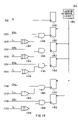
- FIGS. 18 and 19 show an example of the configuration of the clock recovery circuit 1716 .
- the clock recovery circuit 1716 includes plural stages of variable delay elements 1800 , a selector 1802 , a variable delay element 1804 , a phase comparator 1806 , a delay amount control unit 1808 , plural stages of variable delay elements 1814 , a plurality of timing comparators 1816 , plural stages of variable delay elements 1818 , plural stages of variable delay elements 1820 , a selector 1822 , a variable delay element 1824 , a phase comparator 1826 , and a delay amount control unit 1828 .
- the delay amount control unit 1808 includes a counter 1810 and a DAC 1812
- the delay amount control unit 1828 includes a counter 1830 and a DAC 1832 .
- the plural stages of variable delay elements 1814 which are coupled in series sequentially delay a data signal transmitted from the communication device 1700 by a delay amount T.
- the plural stages of variable delay elements 1818 which are coupled in series sequentially delay a clock signal generated by a reception terminal PLL circuit 1718 and delayed by a recovery variable delay circuit 1900 as much as a delay amount T+ ⁇ t which is larger than the delay amount T.
- the plurality of timing comparators 1816 sample each of the plurality of data signals delayed by each of the plural stages of variable delay elements 1814 by the clock signal delayed by the variable delay element 1818 whose stage is the same as each of the plural stages of variable delay elements 1814 .
- each of the plurality of timing comparators 1816 which has the same configuration and function of the timing comparator 100 , samples each of the plurality of data signals (D 0 , D 1 , D 2 , . . . Dn ⁇ 1, Dn) whose delay amounts are different by each of the plurality of clock signals (C 0 , C 1 , C 2 , . . . Cn ⁇ 1, Cn) whose delay amounts are different and outputs the sampling results (Q 0 , Q 1 , Q 2 , . . . Qn ⁇ 1, Qn).
- variable delay elements 1800 which are coupled in series sequentially delay the clock signal generated by the reception terminal PLL circuit 1718 and supply it to the selector 1802 . Further, the plural stages of variable delay elements 1800 have approximately the same delay characteristics as the plural stages of variable delay elements 1814 . And the selector 1802 selects one of the clock signals outputted by the plural stages of variable delay elements 1800 and supplies it to the phase comparator 1806 . And the variable delay element 1804 which is coupled in parallel to the plural stages of variable delay elements 1800 delays the clock signal generated by the reception terminal PLL circuit 1718 as much as a predetermined delay amount and supplies it to the phase comparator 1806 .
- the phase comparator 1806 compares the phase of the clock signal delayed by the plural stages of variable delay elements 1800 , supplied from the selector 1802 , with the phase of the clock signal delayed by the variable delay element 1804 .
- the delay amount control unit 1808 controls the delay amounts of the plural stages of variable delay elements 1800 and the delay amounts of the plural stages of variable delay elements 1814 based on the comparison result of the phase comparator 1806 in order that the phase of the clock signal delayed by the plural stages of variable delay elements 1800 , supplied from the selector 1802 , and the phase of the data signal delayed by the plural stages of variable delay elements 1814 are approximately equal to the phase of the clock signal delayed by the variable delay element 1804 after predetermined cycles.
- variable delay elements 1820 which are coupled in series sequentially delay the clock signal generated by the reception terminal PLL circuit 1718 and supply it to the selector 1822 . Further, the plural stages of variable delay elements 1820 have approximately the same delay characteristics as the plural stages of variable delay elements 1818 .
- the selector 1822 selects one of the clock signals outputted by the plural stages of variable delay elements 1820 and supplies it to the phase comparator 1826 .
- the variable delay element 1824 which is coupled in parallel to the plural stages of variable delay elements 1820 delays the clock signal generated by the reception terminal PLL circuit 1718 as much as a predetermined delay amount and supplies it to the phase comparator 1826 .
- the phase comparator 1826 compares the phase of the clock signal delayed by the plural stages of variable delay elements 1818 supplied from the selector 1822 with the phase of the clock signal delayed by the variable delay element 1824 .
- the delay amount control unit 1828 controls the delay amounts of the plural stages of variable delay elements 1818 and the delay amounts of the plural stages of variable delay elements 1820 based on the comparison result of the phase comparator 1826 in order that the phase of the clock signal delayed by the plural stages of variable delay elements 1818 , supplied from the selector 1822 , and the phase of the data signal delayed by the plural stages of variable delay elements 1820 are approximately equal to the phase of the clock signal delayed by the variable delay element 1824 after predetermined cycles.
- each of the variable delay elements 1800 , the selector 1802 , the variable delay element 1804 , the phase comparator 1806 , the delay amount control unit 1808 , the counter 1810 , the DAC 1812 , and the variable delay elements 1814 has the same configuration and function as the variable delay elements 402 , the selector 403 , the variable delay element 404 , the phase comparator 406 , the delay amount control unit 408 , the counter 410 , the DAC 412 , and the variable delay elements 502 shown in FIG. 5 .
- the clock recovery circuit 1716 includes a recovery variable delay circuit 1900 , a plurality of EOR circuits 1902 , and a timing judging unit 1903 .
- the plurality of EOR circuits 1902 take a set of two sampling results of each of pairs of the sequential timing comparators 1816 and perform exclusive OR operation on the sets of sampling results respectively.
- the timing judging unit 1903 judges the timing of the clock signal generated by the reception terminal PLL circuit 1718 and delayed by the recovery variable delay circuit 1900 in response to the data signal based on the operation result of each of the plurality of EOR circuits 1902 .
- the timing judging unit 1903 judges the timing of the clock signal generated by the reception terminal PLL circuit 1718 delayed by the recovery variable delay circuit 1900 in response to the data signal by detecting the timing of the clock signal, when the timing comparators 1816 sample the pair of sampling results used by the EOR circuit 1902 , which outputs the logic value indicating that the pair of sampling results are different from each other, to perform exclusive OR operation, as the edge of the data signal.
- the recovery variable delay circuit 1900 delays the clock signal generated by the reception terminal PLL circuit 1718 and supplies it to the flip-flop circuit 1712 based on the judgment result of the timing judging unit 1903 .
- the plurality of EOR circuits 1902 have the same configuration and function as the plurality of EOR circuits 1200 shown in FIG. 12 .
- the timing judging unit 1903 includes a plurality of flip-flop circuits 1904 , a buffer 1906 , a first OR circuit 1908 , a third OR circuit 1910 , a FIFO circuit 1914 , a second OR circuit 1912 , and a counter 1916 .
- the buffer 1906 delays the clock signal outputted by the variable delay element 1814 of the last stage and supplies it to each of the plurality of flip-flop circuits 1904 .
- the flip-flop circuit 1904 supplies the operation results of the plurality of EOR circuits 1902 to the first OR circuit 1908 , the third OR circuit 1910 , or the second OR circuit 1912 .
- the plurality of timing comparators 1816 include a first timing comparator group which is a set of the plurality of timing comparators 1816 for sampling the data signal based on the clock signal where the time delayed by the variable delay elements 1818 is a first delay time or less, a second timing comparator group which is a set of the plurality of timing comparators 1816 for sampling the data signal based on the clock signal where the time delayed by the variable delay elements 1818 is a second delay time or more, and a third timing comparator group which is a set of the plurality of timing comparators 1816 for sampling the data signal based on the clock signal where the time delayed by the variable delay elements 1818 is larger than the first delay time and smaller than the second delay time.
- the plurality of EOR circuits 1902 include a first EOR circuit group which is a set of the plurality of EOR circuits 1902 used for exclusive OR operation on the sampling results of the plurality of timing comparators 1816 included in the first timing comparator group, a second EOR circuit group which is a set of the plurality of EOR circuits 1902 used for exclusive OR operation on the sampling results of the plurality of timing comparators 1816 included in the second timing comparator group, and a third EOR circuit group which is a set of the plurality of EOR circuits 1902 used for exclusive OR operation on the sampling results of the plurality of timing comparators 1816 included in the third timing comparator group.
- the first OR circuit 1908 performs OR operation on the operation results of the plurality of EOR circuits 1902 included in the first EOR circuit group and supplies the result to the FIFO circuit 1914 .
- the third OR circuit 1910 performs OR operation on the operation results of the plurality of EOR circuits 1902 included in the second EOR circuit group and supplies the result to the FIFO circuit 1914 .
- the second OR circuit 1912 performs OR operation on the operation results of the plurality of EOR circuits 1902 included in the third EOR circuit group and supplies the result to the FIFO circuit 1914 .
- the first OR circuit 1908 if the edge of the data signal in response to the clock signal is earlier than the first timing, the first OR circuit 1908 outputs a logic value “1”, the third OR circuit 1910 outputs a logic value “0”, and the second OR circuit 1912 outputs a logic value “0”. And if the edge of the data signal in response to the clock signal is later than the first timing and earlier than the second timing, the first OR circuit 1908 outputs the logic value “0”, the third OR circuit 1910 outputs the logic value “1”, and the second OR circuit 1912 outputs the logic value “0”.
- the first OR circuit 1908 outputs the logic value “0”
- the third OR circuit 1910 outputs the logic value “0”
- the second OR circuit 1912 outputs the logic value “1”.
- the FIFO circuit 1914 synchronously enters the logic values outputted the first, third and second OR circuits 1908 , 1910 and 1912 with the clock signal delayed by the buffer 1906 , whereas synchronously retrieving them with the clock signal generated by the reception terminal PLL circuit 1718 and supplying them to the counter 1916 .
- the counter 1916 synchronously counts the number of times each of the first, third and second OR circuits 1908 , 1910 and 1912 outputs the logic value “1” with the clock signal generated by the reception terminal PLL circuit 1718 , if each of the plurality of timing comparators 1816 performs sampling operation a plurality of times on each of the plurality of data signals by each of the plurality of clock signals and each of the plurality of EOR circuits 1902 performs exclusive OR operation so that each of the first, third and second OR circuits 1908 , 1910 and 1912 performs OR operation a plurality of times.
- the recovery variable delay circuit 1900 changes the delay amount of the clock signal generated by the reception terminal PLL circuit 1718 based on the outputs of the first, third and second OR circuits 1908 , 1910 and 1912 , i.e. the count value of the counter 1916 . Particularly, the recovery variable delay circuit 1900 makes the delay amount of the clock signal larger if the first OR circuit 1908 outputs the logic value “1”, does not change the delay amount of the clock signal if the third OR circuit 1910 outputs the logic value “1”, and makes the delay amount of the clock signal smaller if the second OR circuit 1912 outputs the logic value “1”.
- the recovery variable delay circuit 1900 may make the delay amount of the clock signal large if the first OR circuit 1908 outputs the logic value “1”, not change the delay amount of the clock signal if the third OR circuit 1910 outputs the logic value “1”, and make the delay amount of the clock signal small if the second OR circuit 1912 outputs the logic value “1”.
- the recovery variable delay circuit 1900 adjusts the phase of the clock signal in response to the data signal in the above way and performs calibration by BIST (Built In Self Test) or automatic follow-up in order that the phase of the clock signal is near the center of the eye-opening of the data signal.
- the phase of the clock signal in response to the data signal can be accurately detected, and further the phase of the clock signal in response to the data signal is followed up, so that the phase of the clock signal can be adjusted in real time. Therefore, according to the communication device 1702 related to this embodiment, even if the phase of the clock signal is changed by the noise or the change of the environmental conditions and further the eye-opening of the data signal becomes small by such cause as the high frequency loss of the transmission line 1704 , the phase of the clock signal can be automatically regulated near the center of the eye-opening of the data signal, and thereby extremely stable data transmission can be realized.
Landscapes
- Engineering & Computer Science (AREA)
- Computer Networks & Wireless Communication (AREA)
- Signal Processing (AREA)
- Physics & Mathematics (AREA)
- Nonlinear Science (AREA)
- General Engineering & Computer Science (AREA)
- General Physics & Mathematics (AREA)
- Quality & Reliability (AREA)
- Manipulation Of Pulses (AREA)
- Synchronisation In Digital Transmission Systems (AREA)
- Stabilization Of Oscillater, Synchronisation, Frequency Synthesizers (AREA)
Applications Claiming Priority (2)
| Application Number | Priority Date | Filing Date | Title |
|---|---|---|---|
| JP2003-391456 | 2003-11-20 | ||
| JP2003391456 | 2003-11-20 |
Publications (2)
| Publication Number | Publication Date |
|---|---|
| US20050110544A1 US20050110544A1 (en) | 2005-05-26 |
| US6987410B2 true US6987410B2 (en) | 2006-01-17 |
Family
ID=34587483
Family Applications (1)
| Application Number | Title | Priority Date | Filing Date |
|---|---|---|---|
| US10/835,253 Expired - Fee Related US6987410B2 (en) | 2003-11-20 | 2004-04-29 | Clock recovery circuit and communication device |
Country Status (6)
| Country | Link |
|---|---|
| US (1) | US6987410B2 (ja) |
| JP (1) | JP4416737B2 (ja) |
| KR (1) | KR101062493B1 (ja) |
| CN (1) | CN100581095C (ja) |
| DE (1) | DE112004002222T5 (ja) |
| WO (1) | WO2005050904A1 (ja) |
Cited By (6)
| Publication number | Priority date | Publication date | Assignee | Title |
|---|---|---|---|---|
| US20050206417A1 (en) * | 2002-06-19 | 2005-09-22 | Dominique Morche | Delay-locked loop |
| US20050254569A1 (en) * | 2004-05-14 | 2005-11-17 | Afshin Momtaz | System and method for generating equalization coefficients |
| US20080048740A1 (en) * | 2006-07-13 | 2008-02-28 | Yu-Pin Chou | Method and apparatus for generating clock signal |
| US20080150507A1 (en) * | 2006-12-21 | 2008-06-26 | Rohm Co., Ltd. | Switching Regulator |
| US20090096439A1 (en) * | 2007-10-10 | 2009-04-16 | Faraday Technology Corp. | Built-in jitter measurement circuit |
| US11316655B2 (en) * | 2019-11-12 | 2022-04-26 | Samsung Electronics Co., Ltd. | Device and method with wireless communication |
Families Citing this family (21)
| Publication number | Priority date | Publication date | Assignee | Title |
|---|---|---|---|---|
| DE10157437B4 (de) * | 2001-11-23 | 2007-04-26 | Infineon Technologies Ag | Schaltungsanordnung zur Takt- und Datenrückgewinnung aus einem Empfangssignal |
| JP4457074B2 (ja) * | 2003-11-20 | 2010-04-28 | 株式会社アドバンテスト | タイミングコンパレータ、データサンプリング装置、及び試験装置 |
| CA2564679C (en) * | 2004-03-22 | 2015-06-23 | Osiris Therapeutics, Inc. | Mesenchymal stem cells and uses therefor |
| US7171321B2 (en) | 2004-08-20 | 2007-01-30 | Rambus Inc. | Individual data line strobe-offset control in memory systems |
| US7543172B2 (en) | 2004-12-21 | 2009-06-02 | Rambus Inc. | Strobe masking in a signaling system having multiple clock domains |
| US7688672B2 (en) * | 2005-03-14 | 2010-03-30 | Rambus Inc. | Self-timed interface for strobe-based systems |
| JP4536610B2 (ja) * | 2005-07-07 | 2010-09-01 | 株式会社アドバンテスト | 半導体試験装置 |
| JP4928097B2 (ja) * | 2005-07-29 | 2012-05-09 | 株式会社アドバンテスト | タイミング発生器及び半導体試験装置 |
| JP4657053B2 (ja) * | 2005-07-29 | 2011-03-23 | 株式会社アドバンテスト | タイミング発生器及び半導体試験装置 |
| US8121237B2 (en) | 2006-03-16 | 2012-02-21 | Rambus Inc. | Signaling system with adaptive timing calibration |
| US7501905B2 (en) * | 2006-12-13 | 2009-03-10 | Advantest Corporation | Oscillator circuit, PLL circuit, semiconductor chip, and test apparatus |
| WO2008087821A1 (ja) * | 2007-01-15 | 2008-07-24 | Nec Corporation | 回線品質監視の方法およびその回路 |
| KR101081545B1 (ko) | 2007-03-29 | 2011-11-08 | 가부시키가이샤 어드밴티스트 | 복조 장치, 시험장치 및 전자 디바이스 |
| JP2010028342A (ja) * | 2008-07-17 | 2010-02-04 | Sanyo Electric Co Ltd | Dll回路 |
| US8761207B2 (en) | 2009-04-30 | 2014-06-24 | Centurylink Intellectual Property Llc | System and method for advanced adaptive pseudowire |
| CN103973299A (zh) * | 2013-01-29 | 2014-08-06 | 奇景光电股份有限公司 | 数据及时钟恢复装置 |
| KR102087437B1 (ko) * | 2013-06-17 | 2020-03-10 | 에스케이하이닉스 주식회사 | 수신장치를 포함하는 반도체시스템 |
| US9401799B2 (en) * | 2014-08-04 | 2016-07-26 | Stmicroelectronics S.R.L. | Synchronization method, and corresponding device and integrated circuit |
| US10291214B2 (en) | 2017-03-01 | 2019-05-14 | Analog Devices Global Unlimited Company | Feedforward phase noise compensation |
| CN110309588B (zh) * | 2019-06-28 | 2023-05-12 | 西安紫光国芯半导体有限公司 | 一种信号眼图变化模拟装置 |
| CN115328849B (zh) * | 2022-08-10 | 2023-10-03 | 苏州迅芯微电子有限公司 | 一种用于数据发送和接收的芯片组合结构 |
Citations (7)
| Publication number | Priority date | Publication date | Assignee | Title |
|---|---|---|---|---|
| JPH05110550A (ja) | 1991-10-16 | 1993-04-30 | Fujitsu Ltd | スキユーキヤンセル方式 |
| US5430773A (en) * | 1990-07-11 | 1995-07-04 | Bull, S.A. | Data sampling apparatus, and resultant digital data transmission system |
| US5590154A (en) * | 1995-06-26 | 1996-12-31 | Motorola, Inc. | Equalizer circuit and a method for equalizing a continuous signal |
| JPH09224020A (ja) | 1996-02-16 | 1997-08-26 | Nec Eng Ltd | 入力位相差調整回路 |
| JPH1188310A (ja) | 1997-07-15 | 1999-03-30 | Nec Corp | データとクロックの位相調整回路 |
| WO2003036796A1 (fr) | 2001-10-19 | 2003-05-01 | Advantest Corporation | Circuit en boucle a phase asservie, circuit en boucle a retard de phase, generateur de synchronisation, instrument d'essai a semi-conducteurs et circuit integre a semi-conducteurs |
| US6757327B1 (en) * | 2000-10-02 | 2004-06-29 | Lsi Logic Corporation | Serial data communication receiver having adaptive termination resistors |
-
2004
- 2004-04-28 JP JP2005515546A patent/JP4416737B2/ja not_active Expired - Fee Related
- 2004-04-28 KR KR1020067012205A patent/KR101062493B1/ko not_active IP Right Cessation
- 2004-04-28 DE DE112004002222T patent/DE112004002222T5/de not_active Withdrawn
- 2004-04-28 CN CN200480034306A patent/CN100581095C/zh not_active Expired - Fee Related
- 2004-04-28 WO PCT/JP2004/005666 patent/WO2005050904A1/ja active Application Filing
- 2004-04-29 US US10/835,253 patent/US6987410B2/en not_active Expired - Fee Related
Patent Citations (7)
| Publication number | Priority date | Publication date | Assignee | Title |
|---|---|---|---|---|
| US5430773A (en) * | 1990-07-11 | 1995-07-04 | Bull, S.A. | Data sampling apparatus, and resultant digital data transmission system |
| JPH05110550A (ja) | 1991-10-16 | 1993-04-30 | Fujitsu Ltd | スキユーキヤンセル方式 |
| US5590154A (en) * | 1995-06-26 | 1996-12-31 | Motorola, Inc. | Equalizer circuit and a method for equalizing a continuous signal |
| JPH09224020A (ja) | 1996-02-16 | 1997-08-26 | Nec Eng Ltd | 入力位相差調整回路 |
| JPH1188310A (ja) | 1997-07-15 | 1999-03-30 | Nec Corp | データとクロックの位相調整回路 |
| US6757327B1 (en) * | 2000-10-02 | 2004-06-29 | Lsi Logic Corporation | Serial data communication receiver having adaptive termination resistors |
| WO2003036796A1 (fr) | 2001-10-19 | 2003-05-01 | Advantest Corporation | Circuit en boucle a phase asservie, circuit en boucle a retard de phase, generateur de synchronisation, instrument d'essai a semi-conducteurs et circuit integre a semi-conducteurs |
Non-Patent Citations (3)
| Title |
|---|
| Patent Abstracts of Japan publication No. 05-110550, publication date Apr. 30, 1993 (1 page). |
| Patent Abstracts of Japan publication No. 09-224020, publication dated Aug. 26, 1997 (1 page). |
| Patent Abstracts of Japan publication No. 11-088310, publication date Mar. 30, 1999 (1 page). |
Cited By (9)
| Publication number | Priority date | Publication date | Assignee | Title |
|---|---|---|---|---|
| US20050206417A1 (en) * | 2002-06-19 | 2005-09-22 | Dominique Morche | Delay-locked loop |
| US7391244B2 (en) * | 2002-06-19 | 2008-06-24 | Commissariat A L'energie Atomique | Delay-locked loop |
| US20050254569A1 (en) * | 2004-05-14 | 2005-11-17 | Afshin Momtaz | System and method for generating equalization coefficients |
| US20080048740A1 (en) * | 2006-07-13 | 2008-02-28 | Yu-Pin Chou | Method and apparatus for generating clock signal |
| US20080150507A1 (en) * | 2006-12-21 | 2008-06-26 | Rohm Co., Ltd. | Switching Regulator |
| US7548049B2 (en) * | 2006-12-21 | 2009-06-16 | Rohm Co., Ltd. | Switching regulator |
| US20090096439A1 (en) * | 2007-10-10 | 2009-04-16 | Faraday Technology Corp. | Built-in jitter measurement circuit |
| US7912166B2 (en) * | 2007-10-10 | 2011-03-22 | Faraday Technology Corp. | Built-in jitter measurement circuit |
| US11316655B2 (en) * | 2019-11-12 | 2022-04-26 | Samsung Electronics Co., Ltd. | Device and method with wireless communication |
Also Published As
| Publication number | Publication date |
|---|---|
| JP4416737B2 (ja) | 2010-02-17 |
| CN1883153A (zh) | 2006-12-20 |
| US20050110544A1 (en) | 2005-05-26 |
| CN100581095C (zh) | 2010-01-13 |
| KR20060131789A (ko) | 2006-12-20 |
| DE112004002222T5 (de) | 2006-10-19 |
| KR101062493B1 (ko) | 2011-09-05 |
| WO2005050904A1 (ja) | 2005-06-02 |
| JPWO2005050904A1 (ja) | 2007-06-14 |
Similar Documents
| Publication | Publication Date | Title |
|---|---|---|
| US6987410B2 (en) | Clock recovery circuit and communication device | |
| US7071746B2 (en) | Variable delay circuit | |
| US7034723B2 (en) | Timing comparator, data sampling apparatus, and testing apparatus | |
| US6748549B1 (en) | Clocking an I/O buffer, having a selectable phase difference from the system clock, to and from a remote I/O buffer clocked in phase with the system clock | |
| US5663991A (en) | Integrated circuit chip having built-in self measurement for PLL jitter and phase error | |
| US7978109B1 (en) | Output apparatus and test apparatus | |
| US8270225B2 (en) | Data receiving circuit | |
| US5459402A (en) | Delay time measuring circuit | |
| US7773667B2 (en) | Pseudo asynchronous serializer deserializer (SERDES) testing | |
| US7945404B2 (en) | Clock jitter measurement circuit and integrated circuit having the same | |
| US7519844B2 (en) | PVT drift compensation | |
| US20110169501A1 (en) | Delay circuit | |
| US7168020B2 (en) | Circuit and method for testing embedded phase-locked loop circuit | |
| US10983164B2 (en) | Test apparatus | |
| US6282680B1 (en) | Semiconductor device | |
| US8055969B2 (en) | Multi-strobe circuit | |
| US7449931B2 (en) | Duty ratio adjustment | |
| US20100060323A1 (en) | Test circuit and test method | |
| US20080033678A1 (en) | Method and apparatus for testing delay lines | |
| US7855582B2 (en) | Device and method for detecting a timing of an edge of a signal with respect to a predefined edge of a periodic signal |
Legal Events
| Date | Code | Title | Description |
|---|---|---|---|
| AS | Assignment |
Owner name: ADVANTEST CORPORATION, JAPAN Free format text: ASSIGNMENT OF ASSIGNORS INTEREST;ASSIGNORS:SUDA, MASAKATSU;SUDOU, SATOSHI;OKAYASU, TOSHIYUKI;REEL/FRAME:016085/0619;SIGNING DATES FROM 20040929 TO 20041004 |
|
| FEPP | Fee payment procedure |
Free format text: PAYOR NUMBER ASSIGNED (ORIGINAL EVENT CODE: ASPN); ENTITY STATUS OF PATENT OWNER: LARGE ENTITY |
|
| FPAY | Fee payment |
Year of fee payment: 4 |
|
| FPAY | Fee payment |
Year of fee payment: 8 |
|
| FEPP | Fee payment procedure |
Free format text: MAINTENANCE FEE REMINDER MAILED (ORIGINAL EVENT CODE: REM.) |
|
| LAPS | Lapse for failure to pay maintenance fees |
Free format text: PATENT EXPIRED FOR FAILURE TO PAY MAINTENANCE FEES (ORIGINAL EVENT CODE: EXP.) |
|
| STCH | Information on status: patent discontinuation |
Free format text: PATENT EXPIRED DUE TO NONPAYMENT OF MAINTENANCE FEES UNDER 37 CFR 1.362 |
|
| FP | Lapsed due to failure to pay maintenance fee |
Effective date: 20180117 |