US6886076B1 - Semiconductor integrated circuit device having connection pads for superposing expansion memory - Google Patents
Semiconductor integrated circuit device having connection pads for superposing expansion memory Download PDFInfo
- Publication number
- US6886076B1 US6886076B1 US09/497,121 US49712100A US6886076B1 US 6886076 B1 US6886076 B1 US 6886076B1 US 49712100 A US49712100 A US 49712100A US 6886076 B1 US6886076 B1 US 6886076B1
- Authority
- US
- United States
- Prior art keywords
- integrated circuit
- chip
- memory
- pads
- semiconductor integrated
- Prior art date
- Legal status (The legal status is an assumption and is not a legal conclusion. Google has not performed a legal analysis and makes no representation as to the accuracy of the status listed.)
- Expired - Fee Related
Links
Images


Classifications
-
- G—PHYSICS
- G11—INFORMATION STORAGE
- G11C—STATIC STORES
- G11C5/00—Details of stores covered by group G11C11/00
- G11C5/06—Arrangements for interconnecting storage elements electrically, e.g. by wiring
-
- H—ELECTRICITY
- H10—SEMICONDUCTOR DEVICES; ELECTRIC SOLID-STATE DEVICES NOT OTHERWISE PROVIDED FOR
- H10B—ELECTRONIC MEMORY DEVICES
- H10B20/00—Read-only memory [ROM] devices
- H10B20/27—ROM only
-
- H—ELECTRICITY
- H10—SEMICONDUCTOR DEVICES; ELECTRIC SOLID-STATE DEVICES NOT OTHERWISE PROVIDED FOR
- H10P—GENERIC PROCESSES OR APPARATUS FOR THE MANUFACTURE OR TREATMENT OF DEVICES COVERED BY CLASS H10
- H10P74/00—Testing or measuring during manufacture or treatment of wafers, substrates or devices
- H10P74/23—Testing or measuring during manufacture or treatment of wafers, substrates or devices characterised by multiple measurements, corrections, marking or sorting processes
- H10P74/232—Testing or measuring during manufacture or treatment of wafers, substrates or devices characterised by multiple measurements, corrections, marking or sorting processes comprising connection or disconnection of parts of a device in response to a measurement
-
- H—ELECTRICITY
- H10—SEMICONDUCTOR DEVICES; ELECTRIC SOLID-STATE DEVICES NOT OTHERWISE PROVIDED FOR
- H10W—GENERIC PACKAGES, INTERCONNECTIONS, CONNECTORS OR OTHER CONSTRUCTIONAL DETAILS OF DEVICES COVERED BY CLASS H10
- H10W90/00—Package configurations
-
- H—ELECTRICITY
- H10—SEMICONDUCTOR DEVICES; ELECTRIC SOLID-STATE DEVICES NOT OTHERWISE PROVIDED FOR
- H10W—GENERIC PACKAGES, INTERCONNECTIONS, CONNECTORS OR OTHER CONSTRUCTIONAL DETAILS OF DEVICES COVERED BY CLASS H10
- H10W72/00—Interconnections or connectors in packages
- H10W72/01—Manufacture or treatment
-
- H—ELECTRICITY
- H10—SEMICONDUCTOR DEVICES; ELECTRIC SOLID-STATE DEVICES NOT OTHERWISE PROVIDED FOR
- H10W—GENERIC PACKAGES, INTERCONNECTIONS, CONNECTORS OR OTHER CONSTRUCTIONAL DETAILS OF DEVICES COVERED BY CLASS H10
- H10W72/00—Interconnections or connectors in packages
- H10W72/50—Bond wires
- H10W72/541—Dispositions of bond wires
- H10W72/547—Dispositions of multiple bond wires
- H10W72/5473—Dispositions of multiple bond wires multiple bond wires connected to a common bond pad
-
- H—ELECTRICITY
- H10—SEMICONDUCTOR DEVICES; ELECTRIC SOLID-STATE DEVICES NOT OTHERWISE PROVIDED FOR
- H10W—GENERIC PACKAGES, INTERCONNECTIONS, CONNECTORS OR OTHER CONSTRUCTIONAL DETAILS OF DEVICES COVERED BY CLASS H10
- H10W72/00—Interconnections or connectors in packages
- H10W72/90—Bond pads, in general
- H10W72/931—Shapes of bond pads
- H10W72/932—Plan-view shape, i.e. in top view
-
- H—ELECTRICITY
- H10—SEMICONDUCTOR DEVICES; ELECTRIC SOLID-STATE DEVICES NOT OTHERWISE PROVIDED FOR
- H10W—GENERIC PACKAGES, INTERCONNECTIONS, CONNECTORS OR OTHER CONSTRUCTIONAL DETAILS OF DEVICES COVERED BY CLASS H10
- H10W90/00—Package configurations
- H10W90/20—Configurations of stacked chips
- H10W90/284—Configurations of stacked chips characterised by structural arrangements for measuring or testing
-
- H—ELECTRICITY
- H10—SEMICONDUCTOR DEVICES; ELECTRIC SOLID-STATE DEVICES NOT OTHERWISE PROVIDED FOR
- H10W—GENERIC PACKAGES, INTERCONNECTIONS, CONNECTORS OR OTHER CONSTRUCTIONAL DETAILS OF DEVICES COVERED BY CLASS H10
- H10W90/00—Package configurations
- H10W90/701—Package configurations characterised by the relative positions of pads or connectors relative to package parts
- H10W90/751—Package configurations characterised by the relative positions of pads or connectors relative to package parts of bond wires
- H10W90/752—Package configurations characterised by the relative positions of pads or connectors relative to package parts of bond wires between stacked chips
-
- H—ELECTRICITY
- H10—SEMICONDUCTOR DEVICES; ELECTRIC SOLID-STATE DEVICES NOT OTHERWISE PROVIDED FOR
- H10W—GENERIC PACKAGES, INTERCONNECTIONS, CONNECTORS OR OTHER CONSTRUCTIONAL DETAILS OF DEVICES COVERED BY CLASS H10
- H10W90/00—Package configurations
- H10W90/701—Package configurations characterised by the relative positions of pads or connectors relative to package parts
- H10W90/751—Package configurations characterised by the relative positions of pads or connectors relative to package parts of bond wires
- H10W90/754—Package configurations characterised by the relative positions of pads or connectors relative to package parts of bond wires between a chip and a stacked insulating package substrate, interposer or RDL
Definitions
- the present invention relates to expansion of memory in a semiconductor integrated circuit device (hereinafter referred to as an “IC”) incorporating memory.
- IC semiconductor integrated circuit device
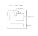
- a conventional IC 30 incorporating memory is composed of a ROM block 31 and other blocks, and, within the IC 30 , the input/output terminals of the ROM block 31 are connected to the other blocks by way of metal conductors 32 .
- the input/output signals to and from the ROM block 31 do not directly appear outside the IC 30 .
- a typical example of such an IC incorporating memory is a microcomputer, which is usually used to control another system.
- a microcomputer which is usually used to control another system.
- programs and data are stored in the ROM and RAM, respectively, incorporated therein.
- the capacity of each type of memory is set to the minimum required by the system in order to minimize the chip cost.
- household electric appliances nowadays tend to undergo frequent renewal or redesigning, with their functions improved or expanded on every such occasion to meet consumers' needs.
- Such functional improvement or expansion of a household electric appliance is usually achieved by rewriting the programs stored in the ROM of the microcomputer built in its control system.
- Japanese Laid-Open Patent Application No. H3-268450 discloses a method of relieving defective blocks in an IC by superposing an auxiliary IC thereon. This method helps avoid making the chip size of the IC or the system board larger. However, this method involves cutting the conductors connecting the defective blocks of the IC to the inside of the IC and keeping the outputs from the defective blocks from appearing outside the IC, and thus, although quite naturally with defective blocks, some blocks are wastefully left unusable.
- An object of the present invention is to provide an IC whose memory capacity can be increased without increasing the chip size thereof when more memory is needed due to an improvement or the like of the functions of a system.
- a semiconductor integrated circuit device i.e. an IC
- This structure makes it possible to select and use only the memory built in the IC as long as it has the desired capacity.
- an expansion memory is added in such a way that either the built-in or expansion memory is selectively used. This makes expansion of memory easy. Since the IC is provided with connection pads, the expansion memory can easily be added thereto.
- the expansion memory may be superposed on the IC, with the connection pads electrically connected to the external connection pads of the expansion memory. Superposing the expansion memory on the IC helps avoid making the chip size larger.
- the above-described IC may be further provided with a disconnecting means for electrically disconnecting the connection pads provided inside the IC from the built-in memory block in accordance with the type of the signal of the switching means for switching between the select signal and the non-select signal.
- the connection pads are prone to cause parasitic capacitance. Electrically disconnecting the connection pads from the built-in memory block helps prevent the influence of such parasitic capacitance when the memory block is being selected.
- the above-described IC may be so designed that addition or modification of a program, if required in a system incorporating the IC, can be achieved by superposing thereon the expansion memory having a program to be added or a modified program stored therein. This helps reduce the modification of the programs stored in the IC to, for example, modifying jump addresses and the like, and thus makes efficient addition or modification of a program possible.
- the above-described IC may be so designed that addition or modification of a program, if required in a system incorporating the IC, can be achieved by simply adding or modifying a program in the expansion memory. This eliminates the need to modify the programs stored in the IC, and thus makes highly efficient addition or modification of a program possible.
- the above-described IC may be further provided with a disconnecting means for electrically disconnecting the connection pads from the built-in memory block when the expansion memory is not superposed on the IC or when the expansion memory is not being selected.
- the connection pads are prone to cause parasitic capacitance, and therefore disconnecting them from the memory block when the expansion memory is not used helps prevent the influence of parasitic capacitance when the built-in memory block is used.
- the expansion memory may have its power pad and ground pad individually connected directly to the power pin and ground pin of a lead frame by way of wires. This structure permits electric power to be supplied directly from the lead frame to the expansion memory, and thus makes it easy to secure the current capacity required by the expansion memory.
- the expansion memory may be provided with pads that are dedicated to the wires laid to achieve direct connection to the power pin and ground pin of the lead frame. Bonding more than one wire to a single pad makes the bonding operation difficult and tends to damage the pad. By contrast, if dedicated pads re provided, wires can be bonded thereto easily without damaging the pads.
- FIG. 1 is a diagram schematically showing the structure of the mother chip of the IC of a first embodiment of the invention
- FIGS. 2A and 2B are diagrams showing an example of the positional relationship between the pads of the mother chip and the pads of the daughter chip in the IC of the first embodiment
- FIG. 3 is a perspective view showing how the daughter chip is superposed on the mother chip in the example shown in FIGS. 2A and 2B ;
- FIG. 4 is a side view showing the daughter chip superposed on the mother chip in the example shown in FIGS. 2A and 2B ;
- FIGS. 5A and 5B are diagrams showing another example of the positional relationship between the pads of the mother chip and the pads of the daughter chip in the IC of the first embodiment
- FIG. 6 is a perspective view showing how the daughter chip is superposed on the mother chip in the example shown in FIGS. 5A and 5B ;
- FIG. 7 is a side view showing the daughter chip superposed on the mother chip in the example shown in FIGS. 5A and 5B ;
- FIG. 8 is a diagram schematically showing the structure related to the control of the ROM block provided on the mother chip and the memory provided on the daughter chip;
- FIG. 9 is a diagram showing an example of how connection to the supplied power and the ground level is achieved when the IC of the first embodiment is formed into an end product;
- FIG. 10 is a diagram showing another example of how connection to the supplied power and the ground level is achieved when the IC of the first embodiment is formed into an end product;
- FIG. 11 is a diagram schematically showing the structure of the IC of a second embodiment of the invention.
- FIG. 12 is a diagram showing an example of the configuration of the switch circuits provided in the mother chip in the second embodiment.
- FIG. 13 is a diagram schematically showing the structure of a conventional IC.
- FIG. 1 shows the IC of a first embodiment of the invention.
- This IC is designed to allow an expansion memory to be superposed thereon at a later time.
- the IC will be referred to as the mother chip and the expansion memory as the daughter chip.
- the mother chip 10 is, like the conventional IC 30 shown in FIG. 13 , composed of a ROM block 11 and other blocks. However, in this embodiment, the input/output terminals of the ROM block 11 are connected to the other blocks within the mother chip 10 by way of metal conductors 12 each having a pad hereon.
- the conductors 12 include those for transferring input signals such as addresses and clocks from the other blocks to the ROM block 11 , those for transferring output signals such as program codes and data from the ROM block 11 to the other blocks, and others.
- the mother chip 10 is composed of greatly varies depending on its use, but it is invariably provided with conductors 12 each having a pad thereon irrespective of what types of blocks it is composed of.
- conductors 12 each having a pad thereon irrespective of what types of blocks it is composed of.
- the pads of the conductors 12 are used to electrically connect the daughter chip to the mother chip 10 .
- FIGS. 2A and 2B show an example of the positions of the pads 13 provided on the conductors 12 that are connected to the ROM block 11 within the mother chip 10 and the positions of the input/output pads 15 provided on the daughter chip 14 .
- the pads 15 of the daughter chip 14 are connected to the input/output terminals of the memory formed inside the chip.
- the daughter chip 14 has roughly the same size (area) as the ROM block 11 .
- the pads 13 are provided near the portion of the surface of the mother chip 10 where the ROM block 11 is formed.
- the pads 15 are provided near the edge of the surface of the daughter chip 14 .
- FIG. 3 shows how the daughter chip 14 is superposed on the mother chip 10 in this example.
- FIG. 4 shows a side view of the daughter chip 14 thus superposed on the mother chip 10 .
- the daughter chip 14 is superposed on and fixed, with an adhesive or the like, to the surface of the portion of the mother chip 10 where the ROM block 11 is provided, with the surface of the daughter chip 14 on which the pads 15 are provided facing opposite the mother chip 10 .
- the pads 13 are connected to the corresponding ones of the pads 15 individually by way of wires 16 .
- FIGS. 5A and 5B show another example of the positions of the pads 13 of the mother chip 10 and the positions of the pads 15 of the daughter chip 14 .
- the daughter chip 14 is made somewhat larger than the ROM block 11 .
- the pads 13 are provided near the portion of the surface of the mother chip 10 where the ROM block 11 is formed.
- the pads 15 are provided near the edge of the surface of the daughter chip 14 .
- FIG. 6 shows how the daughter chip 14 is superposed on the mother chip 10 in this example.
- FIG. 7 shows a side view of the daughter chip 14 thus superposed on the mother chip 10 .
- the daughter chip 14 is superposed above a region 17 that completely encloses the portion of the surface of the mother chip 10 where the ROM block 11 is provided, with the surface of the daughter chip 14 on which the pads 15 are provided facing the mother chip 10 .
- the pads 13 of the mother chip 10 are connected to the pads 15 of the daughter chip 14 by way of solder bumps 18 that are previously provided on the pads 13 .
- the pads 15 of the daughter chip 14 need to be so arranged as to be mirror-symmetrical with the pads 13 of the mother chip 10 .
- This superposition method requires no pads or wires on the surface of the daughter chip 14 after superposition, and thus allows another chip larger than the daughter chip 14 to be superposed further thereon.
- the daughter chip 14 here does not necessarily have to be made larger than the ROM block 11 so as to cover the ROM block 11 completely.
- FIG. 8 shows the structure related to the control of the ROM block 11 provided on the mother chip 10 and the memory provided on the daughter chip 14 .
- the mother chip 10 is provided with a select signal generating circuit 20 , a ROM block select signal line 21 , a ROM block select signal input pad 22 , a daughter chip select signal line 23 , and a daughter chip select signal output pad 24 .
- the daughter chip 14 is provided with a daughter chip select signal input pad 25 .
- the daughter chip select signal output pad 24 of the mother chip 10 is electrically connected to the daughter chip select signal input pad 25 of the daughter chip 14 . This connection is achieved in the same manner as the connection between the pads 13 and 15 .
- the select signal generating circuit 20 generates a ROM block select signal or selecting the ROM block 11 and a daughter chip select signal for selecting the daughter chip 14 on the basis of the memory addresses allocated individually to those two portions of ROM.
- the ROM block select signal generated by the select signal generating circuit 20 is fed, by way of the ROM block select signal line 21 and via the ROM block select signal input pad 22 , to the inside of the ROM block 11 . This brings the ROM block 11 into a state in which it can be accessed for input/output operations, i.e. an enabled state.
- the daughter chip select signal generated by the select signal generating circuit 20 is fed, by way of the daughter chip select signal line 23 , via the daughter chip select signal output pad 24 , and via the daughter chip select signal input pad 25 , to the inside of the daughter chip. This brings the daughter chip 14 into an enabled state.
- the ROM block 11 and the daughter chip 14 may be selected either exclusively or simultaneously. Exclusive selection is achieved by bringing the daughter chip select signal into a non-select state when the ROM block select signal is brought into a select state and bringing the ROM block select signal into a non-select state when the daughter chip select signal is brought into a select state. Whichever of the ROM block 11 and the daughter chip 14 receives its select signal in a non-select state is brought into a disabled state in which it cannot be accessed for input/output operations. Exclusive selection is suitable to read continuously from either of the ROM block 11 and the daughter chip 14 . On the other hand, simultaneous selection is suitable to read alternately from the ROM block 11 and the daughter chip 14 .
- FIG. 9 shows an example of how connection to the supplied power and the ground level is achieved when the IC having the daughter chip 14 superposed on the mother chip 10 is packaged so as to be formed into an end product.
- the mother chip 10 is die-bonded to an island (not shown) of a lead frame having various input/output pins including a power pin 29 a and a ground pin 29 b , and is then sealed in resin.
- the power pin 29 a is connected to a power source that supplies electric power to the IC as an end product, and the ground pin 29 b is connected to a ground level.
- the mother chip 10 is provided with a power pad 26 a and a ground pad 26 b .
- the power pad 26 a and the ground pad 26 b are connected, by way of wires 28 a and 28 b , to the power pin 29 a and the ground pin 29 b , respectively.
- All of the circuits formed on the mother chip 10 including the ROM block 11 operate from the electric power supplied via the power pad 26 a .
- the mother chip 10 is also provided with pads 26 c and 26 d that are, within the mother chip 10 , connected to the power pad 26 a and the ground pad 26 b.
- the daughter chip 14 is provided with a power pad 27 a and a ground pad 27 b .
- the power pad 27 a and the ground pad 27 b are connected, by way of wires 28 c and 28 d , to the pads 26 c and 26 d , respectively, of the mother chip 10 .
- the power pad 27 a and the ground pad 27 b are connected also, by way of wires 28 e and 28 f , to the power pin 29 a and the ground pin 29 b , respectively.
- the daughter chip 14 is connected to the power pin 29 a and the ground pin 29 b both indirectly, i.e. through the mother chip 10 , and directly, independently of the mother chip 10 .
- the daughter chip 14 operates from the electric power supplied via the power pad 27 a.
- Connecting the daughter chip 14 to the power pin 29 a and the ground pin 29 b through the mother chip 10 makes it easy to test the operation of the IC as a whole before packaging.
- connecting the daughter chip 14 directly to the power pin 29 a and the ground pin 29 b helps secure the current capacity required when the IC is used as an end product. It is also possible to connect the daughter chip 14 to the power pin 29 a and the ground pin 29 b only through the mother chip 10 ; in that case, to secure the required current capacity, within the mother chip 10 , the conductor connecting the power pad 26 a to the pad 26 c and the conductor connecting the ground pad 26 b to the pad 26 d need to be made accordingly thick and wide.
- FIG. 10 shows another example of how the mother chip 10 and the daughter chip 14 are connected to the power pin 29 a and the ground pin 29 b .
- another pair of a power pad 27 c and a ground pad 27 d is provided on the daughter chip 14 , and the wires 28 e and 28 f here are connected to the power pad 27 c and the ground pad 27 d .
- the power pads 27 a and 27 c are connected to each other, and the ground pads 27 b and 27 d are connected to each other.
- connection methods described above are applicable also to packaging in which an IC is mounted on an insulating substrate having conductors connected to a supplied power and a ground level.
- FIG. 11 shows the IC of a second embodiment of the invention.
- This IC has a structure similar to that of the IC of the first embodiment. Accordingly, such elements as are found in both embodiments are identified with the same reference numerals, and overlapping descriptions will not be repeated.
- the pads 13 are so formed as to be separate from the metal conductors 12 , and the metal conductors 12 are connected to the pads 13 individually through switch circuits 18 .
- the switch circuits 18 are either in a conducting state or in a non-conducting state at a time, and their states are switched by the daughter chip select signal mentioned previously. When the switch circuits 18 are in a conducting state, the metal conductors 12 are electrically connected to the pads 13 ; when the switch circuits 18 are in a non-conducting state, the metal conductors 12 are electrically disconnected from the pads 13 .
- FIG. 12 shows an example of the configuration of the switch circuits 18 .
- the switch circuits 18 are each composed of a p-channel transistor 18 p , an n-channel transistor 18 n , and an inverter 18 j .
- the transistors 18 p and 18 n have their sources connected together and have their drains connected together, with one node 18 a connected to one of the metal conductors 12 and the other node 18 b connected to one of the pads 13 .
- the n-channel transistor 18 n has its gate connected directly to the daughter chip select signal line 23
- the p-channel transistor 18 p has its gate connected through the inverter 18 j to the daughter chip select signal line 23 .
- the daughter chip select signal When the daughter chip select signal is at a high level, which indicates that it is in a selected state, a high level is fed to the n-channel transistor 18 n and a low level is fed to the p-channel transistor 18 p . This brings both of these transistors 18 n and 18 p into a conducting state and thereby causes the metal conductor 12 to be connected to the pad 13 .
- the daughter chip select signal is at a low level, which indicates that it is in a non-selected state
- a low level is fed to the n-channel transistor 18 n and a high level is fed to the p-channel transistor 18 p .
- the select signal generating circuit 20 which generates the daughter chip select signal and the ROM block select signal, is built as a part of an interface circuit 19 that performs read operations with respect to the ROM block 11 and the daughter chip 14 .
- the select signal generating circuit 20 brings the daughter chip select signal into a selected or non-selected state in accordance with whether the interface circuit 19 performs read operations with respect to the daughter chip 14 or not.
- the select signal generating circuit 20 keeps the daughter chip select signal in a non-selected state all the time.
- the pads 13 are connected to the metal conductors 12 only when the daughter chip 14 is superposed on the mother chip 10 and in addition the daughter chip 14 is selected. Since the pads 13 have appreciable areas, they are prone to cause parasitic capacitance. However, by electrically disconnecting the pads 13 from the metal conductors 12 , it is possible to prevent the influence of such parasitic capacitance on the input/output signals to and from the ROM block. That is, it is possible to prevent delay or waveform rounding in the input/output signals to and from the ROM block. This permits the IC to offer sufficiently high reliability.
Landscapes
- Dram (AREA)
- Semiconductor Memories (AREA)
Applications Claiming Priority (2)
| Application Number | Priority Date | Filing Date | Title |
|---|---|---|---|
| JP12154199 | 1999-04-28 | ||
| JP2000010025A JP3669889B2 (ja) | 1999-04-28 | 2000-01-13 | 半導体集積回路装置 |
Publications (1)
| Publication Number | Publication Date |
|---|---|
| US6886076B1 true US6886076B1 (en) | 2005-04-26 |
Family
ID=26458885
Family Applications (1)
| Application Number | Title | Priority Date | Filing Date |
|---|---|---|---|
| US09/497,121 Expired - Fee Related US6886076B1 (en) | 1999-04-28 | 2000-02-03 | Semiconductor integrated circuit device having connection pads for superposing expansion memory |
Country Status (2)
| Country | Link |
|---|---|
| US (1) | US6886076B1 (ja) |
| JP (1) | JP3669889B2 (ja) |
Cited By (5)
| Publication number | Priority date | Publication date | Assignee | Title |
|---|---|---|---|---|
| CN100547784C (zh) * | 2005-12-16 | 2009-10-07 | 晨星半导体股份有限公司 | 多芯片封装结构的内连线 |
| US20130026656A1 (en) * | 2009-04-27 | 2013-01-31 | Kim Hye-Jin | Semiconductor packages and electronic systems including the same |
| CN103229293A (zh) * | 2010-10-19 | 2013-07-31 | Nepes株式会社 | 半导体芯片封装、半导体模块及其制造方法 |
| US8981574B2 (en) | 2012-12-20 | 2015-03-17 | Samsung Electronics Co., Ltd. | Semiconductor package |
| US9823846B2 (en) | 2014-08-20 | 2017-11-21 | Qualcomm Incorporated | Systems and methods for expanding memory for a system on chip |
Families Citing this family (4)
| Publication number | Priority date | Publication date | Assignee | Title |
|---|---|---|---|---|
| JP3737333B2 (ja) | 2000-03-17 | 2006-01-18 | 沖電気工業株式会社 | 半導体装置 |
| JP4054200B2 (ja) | 2002-02-19 | 2008-02-27 | 松下電器産業株式会社 | 半導体記憶装置 |
| JP4649827B2 (ja) * | 2003-09-26 | 2011-03-16 | セイコーエプソン株式会社 | 液体噴射装置およびその製造方法 |
| JP4808979B2 (ja) * | 2005-03-18 | 2011-11-02 | 株式会社リコー | マルチチップ型半導体装置及びその製造方法 |
Citations (8)
| Publication number | Priority date | Publication date | Assignee | Title |
|---|---|---|---|---|
| US3753235A (en) * | 1971-08-18 | 1973-08-14 | Ibm | Monolithic memory module redundancy scheme using prewired substrates |
| JPH03268450A (ja) | 1990-03-19 | 1991-11-29 | Fujitsu Ltd | ウエハースケールの欠陥ic救済方法 |
| US5214570A (en) * | 1992-04-03 | 1993-05-25 | Clearpoint Research Corporation | Compact memory module |
| US5514907A (en) * | 1995-03-21 | 1996-05-07 | Simple Technology Incorporated | Apparatus for stacking semiconductor chips |
| US5677877A (en) * | 1995-05-25 | 1997-10-14 | Samsung Electronics Co., Ltd. | Integrated circuit chips with multiplexed input/output pads and methods of operating same |
| US6026039A (en) * | 1997-12-20 | 2000-02-15 | Samsung Electronics Co., Ltd. | Parallel test circuit for semiconductor memory |
| US6043430A (en) * | 1997-03-14 | 2000-03-28 | Lg Semicon Co., Ltd. | Bottom lead semiconductor chip package |
| US6233157B1 (en) * | 1998-11-07 | 2001-05-15 | Hyundai Electronics Industries Co., Ltd. | Printed circuit board and method for wiring signal lines on the same |
-
2000
- 2000-01-13 JP JP2000010025A patent/JP3669889B2/ja not_active Expired - Fee Related
- 2000-02-03 US US09/497,121 patent/US6886076B1/en not_active Expired - Fee Related
Patent Citations (8)
| Publication number | Priority date | Publication date | Assignee | Title |
|---|---|---|---|---|
| US3753235A (en) * | 1971-08-18 | 1973-08-14 | Ibm | Monolithic memory module redundancy scheme using prewired substrates |
| JPH03268450A (ja) | 1990-03-19 | 1991-11-29 | Fujitsu Ltd | ウエハースケールの欠陥ic救済方法 |
| US5214570A (en) * | 1992-04-03 | 1993-05-25 | Clearpoint Research Corporation | Compact memory module |
| US5514907A (en) * | 1995-03-21 | 1996-05-07 | Simple Technology Incorporated | Apparatus for stacking semiconductor chips |
| US5677877A (en) * | 1995-05-25 | 1997-10-14 | Samsung Electronics Co., Ltd. | Integrated circuit chips with multiplexed input/output pads and methods of operating same |
| US6043430A (en) * | 1997-03-14 | 2000-03-28 | Lg Semicon Co., Ltd. | Bottom lead semiconductor chip package |
| US6026039A (en) * | 1997-12-20 | 2000-02-15 | Samsung Electronics Co., Ltd. | Parallel test circuit for semiconductor memory |
| US6233157B1 (en) * | 1998-11-07 | 2001-05-15 | Hyundai Electronics Industries Co., Ltd. | Printed circuit board and method for wiring signal lines on the same |
Cited By (11)
| Publication number | Priority date | Publication date | Assignee | Title |
|---|---|---|---|---|
| CN100547784C (zh) * | 2005-12-16 | 2009-10-07 | 晨星半导体股份有限公司 | 多芯片封装结构的内连线 |
| US20130026656A1 (en) * | 2009-04-27 | 2013-01-31 | Kim Hye-Jin | Semiconductor packages and electronic systems including the same |
| US8643193B2 (en) * | 2009-04-27 | 2014-02-04 | Samsung Electronics Co., Ltd. | Semiconductor packages and electronic systems including the same |
| US8901749B2 (en) | 2009-04-27 | 2014-12-02 | Samsung Electronics Co., Ltd. | Semiconductor packages and electronic systems including the same |
| CN103229293A (zh) * | 2010-10-19 | 2013-07-31 | Nepes株式会社 | 半导体芯片封装、半导体模块及其制造方法 |
| US20130241042A1 (en) * | 2010-10-19 | 2013-09-19 | Nepes Corporation | Semiconductor chip package, semiconductor module, and method for manufacturing same |
| US9006872B2 (en) * | 2010-10-19 | 2015-04-14 | Nepes Corporation | Semiconductor chip package having via hole and semiconductor module thereof |
| CN103229293B (zh) * | 2010-10-19 | 2016-05-18 | Nepes株式会社 | 半导体芯片封装、半导体模块及其制造方法 |
| US8981574B2 (en) | 2012-12-20 | 2015-03-17 | Samsung Electronics Co., Ltd. | Semiconductor package |
| US9633973B2 (en) | 2012-12-20 | 2017-04-25 | Samsung Electronics Co., Ltd. | Semiconductor package |
| US9823846B2 (en) | 2014-08-20 | 2017-11-21 | Qualcomm Incorporated | Systems and methods for expanding memory for a system on chip |
Also Published As
| Publication number | Publication date |
|---|---|
| JP3669889B2 (ja) | 2005-07-13 |
| JP2001015680A (ja) | 2001-01-19 |
Similar Documents
| Publication | Publication Date | Title |
|---|---|---|
| JP2605687B2 (ja) | 半導体装置 | |
| US5646451A (en) | Multifunctional chip wire bonds | |
| US6417721B2 (en) | Device and method for limiting the extent to which circuits in integrated circuit dice electrically load bond pads and other circuit nodes in the dice | |
| US20050024093A1 (en) | Communication device for a logic circuit | |
| US6886076B1 (en) | Semiconductor integrated circuit device having connection pads for superposing expansion memory | |
| US10387690B2 (en) | Integrated power supply scheme for powering memory card host interface | |
| US20010035568A1 (en) | Lead frame for a semiconductor chip package, semiconductor chip package incorporating multiple integrated circuit chips, and method of fabricating a semiconductor chip package with multiple integrated circuit chips | |
| JP2007184650A (ja) | プログラム可能な電子処理装置用のマウント | |
| US5898225A (en) | Lead frame bonding power distribution systems | |
| US6560157B2 (en) | Semiconductor device | |
| US20030193349A1 (en) | Semiconductor integrated circuit | |
| EP0855742A1 (en) | Semiconductor integrated circuit device produced from master slice and having operation mode easily changeable after selection on master slice | |
| JP2885456B2 (ja) | 集積回路用の給電ピン配置 | |
| US6453421B1 (en) | Processor system with power supply selection mechanism | |
| WO2006011292A1 (ja) | 半導体装置 | |
| KR100594142B1 (ko) | 분리된 전원 링을 가지는 저전력 반도체 칩과 그 제조 및제어방법 | |
| KR100416920B1 (ko) | 본딩패드옵션을구비한집적회로및본딩패드옵션을실행하는방법 | |
| KR19990023594A (ko) | 반도체 소자 및 그 테스트 및 동작 방법 | |
| US6822921B2 (en) | Semiconductor device having semiconductor memory | |
| KR100452326B1 (ko) | 반도체 메모리장치의 동작전압 모드 선택 방법 | |
| US6603219B2 (en) | Semiconductor integrated circuit | |
| JPH11111913A (ja) | 機能変更可能な半導体装置 | |
| JP3447553B2 (ja) | 半導体パッケ−ジ | |
| KR20010065148A (ko) | 입력 모드 선택 회로 | |
| US6936911B1 (en) | Semiconductor integrated circuit device |
Legal Events
| Date | Code | Title | Description |
|---|---|---|---|
| AS | Assignment |
Owner name: SHARP KABUSHIKI KAISHA, JAPAN Free format text: ASSIGNMENT OF ASSIGNORS INTEREST;ASSIGNORS:ISODONO, KOJI;SAITO, HITOSHI;TANAKA, TOYOHIKO;AND OTHERS;REEL/FRAME:010548/0340 Effective date: 20000114 |
|
| FEPP | Fee payment procedure |
Free format text: PAYOR NUMBER ASSIGNED (ORIGINAL EVENT CODE: ASPN); ENTITY STATUS OF PATENT OWNER: LARGE ENTITY |
|
| FPAY | Fee payment |
Year of fee payment: 4 |
|
| FPAY | Fee payment |
Year of fee payment: 8 |
|
| REMI | Maintenance fee reminder mailed | ||
| LAPS | Lapse for failure to pay maintenance fees | ||
| STCH | Information on status: patent discontinuation |
Free format text: PATENT EXPIRED DUE TO NONPAYMENT OF MAINTENANCE FEES UNDER 37 CFR 1.362 |
|
| FP | Lapsed due to failure to pay maintenance fee |
Effective date: 20170426 |