US6548962B1 - Gas discharge panel - Google Patents
Gas discharge panel Download PDFInfo
- Publication number
- US6548962B1 US6548962B1 US09/485,469 US48546900A US6548962B1 US 6548962 B1 US6548962 B1 US 6548962B1 US 48546900 A US48546900 A US 48546900A US 6548962 B1 US6548962 B1 US 6548962B1
- Authority
- US
- United States
- Prior art keywords
- discharge
- gap width
- gas
- electrode
- pair
- Prior art date
- Legal status (The legal status is an assumption and is not a legal conclusion. Google has not performed a legal analysis and makes no representation as to the accuracy of the status listed.)
- Expired - Fee Related
Links
Images


Classifications
-
- H—ELECTRICITY
- H01—ELECTRIC ELEMENTS
- H01J—ELECTRIC DISCHARGE TUBES OR DISCHARGE LAMPS
- H01J11/00—Gas-filled discharge tubes with alternating current induction of the discharge, e.g. alternating current plasma display panels [AC-PDP]; Gas-filled discharge tubes without any main electrode inside the vessel; Gas-filled discharge tubes with at least one main electrode outside the vessel
- H01J11/20—Constructional details
- H01J11/22—Electrodes, e.g. special shape, material or configuration
-
- H—ELECTRICITY
- H01—ELECTRIC ELEMENTS
- H01J—ELECTRIC DISCHARGE TUBES OR DISCHARGE LAMPS
- H01J11/00—Gas-filled discharge tubes with alternating current induction of the discharge, e.g. alternating current plasma display panels [AC-PDP]; Gas-filled discharge tubes without any main electrode inside the vessel; Gas-filled discharge tubes with at least one main electrode outside the vessel
- H01J11/10—AC-PDPs with at least one main electrode being out of contact with the plasma
- H01J11/12—AC-PDPs with at least one main electrode being out of contact with the plasma with main electrodes provided on both sides of the discharge space
-
- H—ELECTRICITY
- H01—ELECTRIC ELEMENTS
- H01J—ELECTRIC DISCHARGE TUBES OR DISCHARGE LAMPS
- H01J11/00—Gas-filled discharge tubes with alternating current induction of the discharge, e.g. alternating current plasma display panels [AC-PDP]; Gas-filled discharge tubes without any main electrode inside the vessel; Gas-filled discharge tubes with at least one main electrode outside the vessel
- H01J11/20—Constructional details
- H01J11/22—Electrodes, e.g. special shape, material or configuration
- H01J11/24—Sustain electrodes or scan electrodes
-
- H—ELECTRICITY
- H01—ELECTRIC ELEMENTS
- H01J—ELECTRIC DISCHARGE TUBES OR DISCHARGE LAMPS
- H01J11/00—Gas-filled discharge tubes with alternating current induction of the discharge, e.g. alternating current plasma display panels [AC-PDP]; Gas-filled discharge tubes without any main electrode inside the vessel; Gas-filled discharge tubes with at least one main electrode outside the vessel
- H01J11/20—Constructional details
- H01J11/22—Electrodes, e.g. special shape, material or configuration
- H01J11/30—Floating electrodes
-
- H—ELECTRICITY
- H01—ELECTRIC ELEMENTS
- H01J—ELECTRIC DISCHARGE TUBES OR DISCHARGE LAMPS
- H01J11/00—Gas-filled discharge tubes with alternating current induction of the discharge, e.g. alternating current plasma display panels [AC-PDP]; Gas-filled discharge tubes without any main electrode inside the vessel; Gas-filled discharge tubes with at least one main electrode outside the vessel
- H01J11/20—Constructional details
- H01J11/22—Electrodes, e.g. special shape, material or configuration
- H01J11/32—Disposition of the electrodes
-
- H—ELECTRICITY
- H01—ELECTRIC ELEMENTS
- H01J—ELECTRIC DISCHARGE TUBES OR DISCHARGE LAMPS
- H01J2211/00—Plasma display panels with alternate current induction of the discharge, e.g. AC-PDPs
- H01J2211/20—Constructional details
- H01J2211/22—Electrodes
- H01J2211/24—Sustain electrodes or scan electrodes
- H01J2211/245—Shape, e.g. cross section or pattern
-
- H—ELECTRICITY
- H01—ELECTRIC ELEMENTS
- H01J—ELECTRIC DISCHARGE TUBES OR DISCHARGE LAMPS
- H01J2211/00—Plasma display panels with alternate current induction of the discharge, e.g. AC-PDPs
- H01J2211/20—Constructional details
- H01J2211/22—Electrodes
- H01J2211/32—Disposition of the electrodes
- H01J2211/323—Mutual disposition of electrodes
Definitions
- the present invention relates to a gas discharge panel used for a display device or the like. More particularly, the present invention relates to a PDP.
- CTR Cathode Ray Tube
- LCD Liquid Crystal Display
- PDP Plasma Display Panel
- CRTs have been widely used as TV displays and excel in resolution and picture quality.
- the depth and weight increase as the screen size increases. Solution of this problem is a key to the production of large-screen CRTs. Therefore, it is considered that producing CRTs having a large screen size exceeding 40 inch is difficult.
- LCDs have found wide spread use as monitors for computers due to excellent characteristics such as smaller power consumption, size, and weight than CRTs.
- large-screen LCDs have such technical problems to be solved as faint images and disordered gray-scale levels or color gradations which are caused because LCDs themselves do not emit light when displaying images.
- a defect of narrow viewing angles which is unique to LCDs, must be cleared in order to achieve large-screen LCDs.
- PDPs unlike CRTs or LCDs, PDPs have an advantage that large-screen PDPs can be achieved with relatively small weights. Also, PDPs have a merit that they consume smaller electricity in spite of the driving method in which PDPs themselves emit light for displaying images. Therefore, at the present time when next-generation displays are sought for, large-screen gas discharge panels such as PDPs are especially studied and developed eagerly. Gas discharge panels with a 50-inch or more screen have already been developed.
- DC Direct Current
- AC Alternating Current
- the technique for restricting power consumption by improving the discharge efficiency has room for refinement in discharge panels such as PDPs.
- a gas discharge panel in which a plurality of cells filled with a discharge gas are arranged as a matrix between a pair of opposed plates, and in which a pair of display electrodes on a surface of one of the pair of opposed plates extend across a plurality of cells in the direction of rows, where a gap between the pair of display electrodes has a first discharge gap width and a second discharge gap width larger than the first discharge gap width.
- the first discharge gap width is determined from approximately the minimum discharge start voltage in a Paschen's curve which shows a relationship between product p ⁇ d and discharge start voltage
- the second discharge gap width is determined from the maximum discharge efficiency in a discharge efficiency curve which shows a relationship between the product p ⁇ d and discharge efficiency, where p represents discharge gas pressure and d represents discharge gap width.
- the above gas discharge panel may take the following specific forms: one of the pair of display electrodes is branched into a first electrode prong and a second electrode prong, the other of the pair of display electrodes is positionally between the first electrode prong and the second electrode prong, a gap width between the first electrode prong and the other display electrode is the first discharge gap width, and a gap width between the second electrode prong and the other display electrode is the second discharge gap width; or each of the pair of display electrodes is branched into a plurality of electrode prongs, a predetermined electrode prong of one of the pair of display electrodes is positionally between a first electrode prong and a second electrode prong of the other of the pair of display electrodes, a gap width between the first electrode prong and the predetermined electrode prong is the first discharge gap width, and a gap width between the second electrode prong and the predetermined electrode prong is the second discharge gap width.
- the above gas discharge panel may take the following form: a gap between the pair of display electrodes has a plurality of gap widths in a direction perpendicular to a surface of the gas discharge panel, the plurality of gap widths including the first discharge gap width and the second discharge gap width.
- the above construction facilitates the formation of the first discharge gap width and the second discharge gap width in a limited space. This is advantageous in producing highly minute cells.
- the above gas discharge panel may take the following form: at least one of facing sides of the pair of display electrodes has one or more projections per cell, the first discharge gap width being formed between the one or more projections and the other of the pair of display electrodes, and the second discharge gap width being formed between the other of the pair of display electrodes and the at least one of facing sides of the pair of display electrodes at portions other than the one or more projections.
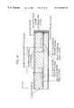
- FIG. 1 is a partial, cross sectional perspective view of the PDP of Embodiment 1.
- FIG. 2 is a top plan view showing a display electrode disposition pattern of the PDP of Embodiment 1.
- FIG. 3 is a top plan view showing a display electrode disposition pattern of a variation of Embodiment 1.
- FIG. 4 is a partial, cross sectional perspective view of the PDP of Embodiment 2.
- FIG. 5 is a partial, cross sectional view of display electrodes and their periphery of the PDP of Embodiment 2.
- FIG. 6 is a partial, cross sectional view of display electrodes and their periphery of a variation of Embodiment 2.
- FIG. 7 is a partial, cross sectional view of display electrodes.and their periphery of a variation of Embodiment 2.
- FIG. 8 is a partial, cross sectional view of display electrodes and their periphery of a variation of Embodiment 2.
- FIG. 9 is a partial, cross sectional view of display electrodes and their periphery of a variation of Embodiment 2.
- FIG. 10 is a partial, cross sectional view of display electrodes and their periphery of a variation of Embodiment 2.
- FIG. 11 is a partial, cross sectional perspective view of the PDP of Embodiment 3.
- FIG. 12 is a top plan view showing a display electrode disposition pattern of the PDP of Embodiment 3.
- FIG. 13 is a top plan view showing a display electrode disposition pattern of a variation of Embodiment 3.
- FIG. 14 is a top plan view showing a display electrode disposition pattern of a variation of Embodiment 3.
- FIG. 15 is a top plan view showing a display electrode disposition pattern of the PDP of Embodiment 4.
- FIG. 16 is a cross sectional view of display electrodes and their periphery of the PDP of Embodiment 4.
- FIG. 17 is a cross sectional view of display electrodes and their periphery of a variation of Embodiment 4.
- FIG. 18 is a cross sectional view of display electrodes and their periphery of the PDP of Embodiment 5.
- FIG. 19 is a graph showing changes with time of applied current and applied voltage when resistance of display electrodes is low.
- FIG. 20 is a graph showing changes with time of applied current and applied voltage when resistance of display electrodes is high.
- FIG. 21 is a cross sectional view of display electrodes and their periphery of a variation of Embodiment 5.
- FIG. 22 is a top plan view showing a display electrode disposition pattern of a variation of Embodiment 5.
- FIGS. 23A, 23 B, and 23 C are graphs showing characteristics (Paschen's curve) of discharge start voltage vs. Product p ⁇ d.
- FIG. 23A shows the Paschen's curve when the percentage of Xe in the discharge gas is 5%.
- FIG. 23B shows the Paschen's curve when the percentage of Xe in the discharge gas is 10%.
- FIG. 23C shows the Paschen's curve when the percentage of Xe in the discharge gas is 2%.
- FIGS. 24A, 24 B, and 24 C are graphs showing characteristics (discharge efficiency curve) of discharge efficiency vs. Product pad.
- FIG. 24A shows the discharge efficiency curve when the percentage of Xe in the discharge gas is 5%.
- FIG. 24B shows the discharge efficiency curve when the percentage of Xe in the discharge gas is 10%.
- FIG. 24C shows the discharge efficiency curve when the perceentage of Xe in the discharge gas is 2%.
- FIG. 1 is a partial, cross sectional perspective view of the AC surface-discharge type PDP of Embodiment 1.
- the thickness of the PDP goes along the direction of z, the xy plane is parallel to the surface of the PDP.
- the PDP is mainly provided with a front panel 20 and a back panel 26 .
- a front panel glass 21 which is a substrate of the front panel 20 , is made of soda-lime glass.
- a pair of fork-shaped display electrodes 22 and 23 (X electrode 22 and Y electrode 23 ) is disposed on a surface of the front panel glass 21 facing the back panel 26 , the display electrodes extending in the direction of x.
- the X electrode 22 has prongs X 1 and X 2 ;
- the Y electrode 23 has prongs Y 1 , Y 2 , and Y 3 .
- the prongs of the display electrodes 22 and 23 are alternately arranged in the direction of y in the order of Y 1 , X 1 , Y 2 , X 2 , and Y 3 .
- the X electrode 22 operates as a scanning electrode during an address discharge.
- the general view of the display electrodes 22 and 23 will be described later.
- the surface of the front panel 20 on which the display electrodes 22 and 23 are disposed is coated with a dielectric layer 24 made of lead oxide base glass. This mean that the display electrodes 22 and 23 are embedded in the dielectric layer 24 .
- An outer surface of the dielectric layer 24 is coated with a protection layer 25 made of magnesium oxide (MgO).
- a back panel glass 27 which is a substrate of the back panel 26 , is manufactured in the same way as the front panel glass 21 .
- a plurality of address electrodes 28 are disposed on a surface of the back panel glass 27 facing the front panel 20 , the address electrodes 28 extending in the direction of y. With a certain distance in the direction of z, the address electrodes 28 and the display electrodes 22 and 23 form a latticelike electrode disposition patten, when viewed from above.
- a dielectric membrane 29 made of the same material as the dielectric layer 24 is formed on the surface of the back panel glass 27 .
- the address electrodes 28 is coated with the dielectric membrane 29 .
- a plurality of barrier ribs 30 are formed along the direction of y on an outer surface of the dielectric membrane 29 , where each of the barrier ribs 30 has a certain height and a certain thickness, and the barrier ribs 30 and the address electrodes 28 are formed. Sides of the ribs 30 and the bottom of the space between the ribs 30 on the dielectric membrane 29 are coated with phosphor layers 31 to 33 corresponding to red, green, and blue.
- the protection layer 25 of the front panel 20 and the top of the barrier ribs 30 of the back panel 26 are bonded together with a sealing glass.
- Each space partitioned by the plurality of barrier ribs 30 is filled with a discharge gas including a rare gas, rendering each space a swath of discharge space 38 extending along the direction of y.
- Each area of the discharge space 38 intersecting with a pair of display electrodes 22 and 23 (in Embodiment 1, electrode prongs X 1 , X 2 , Y 1 , Y 2 , and Y 3 ) is called a cell.
- Cells 11 to 14 are examples of such cells and will be described later.
- the cells 11 , . . . as a whole form a matrix with rows in the x direction and columns in the y direction. It is possible for the present PDP to perform a matrix display by allowing each cell 11 , . . . to emit light as required.
- each of the electrodes 22 , 23 , 28 electricity is supplied to each of the electrodes 22 , 23 , 28 to establish two kinds of discharges: an address discharge in which electricity is supplied to space between the address electrode 28 and either of the X electrode 22 or the Y electrode 23 to control ON/OFF of light emission for each of the cells 11 , . . . ; and a sustain discharge (surface discharge) in which electricity is supplied to space between each pair of the X electrode 22 and the Y electrode 23 .
- FIG. 2 is a top plan view showing a display electrode disposition pattern of the present PDP viewed from above in the direction of z.
- the barrier ribs 30 are omitted from the drawing for simplification.
- Each area of the discharge space 38 encircled with a dotted line is cell 11 , 12 , 13 , or 14 .
- the electrode prongs Y 1 , X 1 , Y 2 , X 2 , and Y 3 (Y′ 1 , X′ 1 , Y′ 2 , X′ 2 , and Y′ 3 ) disposed in this order and corresponding to the cell 11 (cell 12 ) are each approximately 20 ⁇ m in width.
- the discharge gap width between the electrode prongs is either of the following two values:
- a first.discharge gap width 39 of approximately 20 ⁇ m such as a gap width between prongs X 1 and Y 2 and a gap width between prongs Y 2 and X 2 (a gap width between prongs Y′ 1 and X′ 1 and a gap width between prongs Y′ 2 and X′ 2 ).
- the first discharge gap width 39 is set in order to restrict the discharge start voltage to a lower value than conventional techniques.
- a second discharge gap width 40 of approximately 40 ⁇ m such as a gap width between prongs Y 1 and X 1 and a gap width between prongs X 2 and Y 3 (a gap width between prongs Y′ 1 and X′ 1 and a gap width between prongs X′ 2 and Y′ 3 ).
- the second discharge gap width 40 is set in order to secure a high light emission efficiency after the discharge start.
- a gap width 35 between the two cells 11 and 12 (cells 13 and 14 ) adjoining in the y direction and a gap width between prongs Y 3 and Y′ 1 of the Y electrodes are each set to approximately 120 ⁇ m.
- the surface discharge (initial discharge) starts in a space having the first discharge gap width 39 .
- the discharge start voltage is lower than conventional techniques. This effectively restricts the power consumption of the PDP at the initial discharge.
- the PDP of the present embodiment performs the initial discharge and the sustain discharge using the discharge gap widths between the prongs X 1 , . . . properly in correspondence to each discharge.
- more Y electrode prongs are provided than X electrode prongs in the dielectric layer 24 .
- three Y electrode prongs Y 1 , Y 2 , and Y 3 and two X electrode prongs X 1 and X 2 are disposed in the cell 11 , the Y electrode prongs exceeding the X electrode prongs by one in the number. This prevents a cross talk from occurring between the prong X 2 of the cell 11 and the prong Y′ 1 of the adjacent cell 12 , for example. That is to say, the X electrode 22 , which also acts as a scanning electrode, is protected by the Y electrode 23 .
- the PDP with the above construction is manufactured as follows.
- the fork-shaped display electrodes 22 and 23 respectively having prongs X 1 and X 2 and Y 1 , Y 2 , and Y 3 are formed on a surface of the front panel glass 21 which is made of soda-lime glass and being approximately 2 mm in thickness, the display electrodes 22 and 23 being made of an electrically conductive, silver base material.
- a known method such as the screen printing method or the photo-etching method can be used to produce the fork-shaped display electrodes 22 and 23 .
- the dielectric layer 24 is then formed by applying a paste of lead base glass to the surface of display electrodes 22 and 23 as a whole so as to form a coat approximately 20 ⁇ m to 30 ⁇ m in thickness, and by baking the formed coat.
- the front panel 20 is complete after the protection layer 25 approximately 1 ⁇ m in thickness made of magnesium oxide (MgO) is formed on the dielectric layer 24 with the vapor deposition or CVD (chemical vapor deposition) method.
- MgO magnesium oxide
- the address electrodes 28 approximately 5 ⁇ m in thickness are formed by applying an electrically conductive, silver base material on a surface of the back panel glass 27 in stripes with a certain pitch with the screen printing method, the back panel glass 27 being made of soda-lime glass and approximately 2 mm in thickness.
- the PDP is manufactured for a 40-inch-class high definition TV.
- the distance between adjoining address electrodes 28 is set to approximately 0.2 mm or less.
- the dielectric membrane 29 is then formed by applying a paste of lead base glass to the surface of the back panel glass 27 as a whole, on which the address electrodes 28 have been formed, to form a coat of approximately 20 cm to 30 ⁇ m in thickness, and by baking the coat.
- the barrier ribs 30 made of the same lead base glass as the dielectric membrane 29 and approximately 100 ⁇ m in height are then formed between each pair of adjoining address electrodes 28 .
- the barrier ribs 30 are formed, for example, by repeatedly coating a paste of the lead base glass with the screen printing method and baking the coated paste.
- the phosphor layers 31 , 32 , and 33 are formed on sides of the barrier ribs 30 and the exposed surface of the dielectric membrane 29 between the barrier ribs 30 by applying phosphor ink for each of the three colors, red, green, and blue thereto, and drying and baking the applied ink.
- the back panel 26 is completed with the above step.
- soda-lime glass which is introduced as the material of the front panel glass 21 and the back panel glass 27 , may be replaced with other materials.
- the dielectric layer 24 and the protection layer 25 may be made of materials other than the specific ones described above. This is the same for the display electrodes 22 and 23 , and for example, other materials may be selected to achieve excellent transparency of the display electrodes 22 and 23 . In this way, it is possible to select various materials in a possible range for each embodiment.
- the front panel 20 completed as above is bonded to the back panel 26 with the sealing glass. Gas is released from the discharge space to produce a high vacuum (8 ⁇ 10 ⁇ 7 Torr), then the discharge space is filled with a Ne—Xe(5%) base discharge gas through the application of a certain pressure (in this example, 2000 Torr). This completes the PDP.
- the description of the production of PDP will be mainly composed of characteristics of the display electrodes since most of the PDP production procedure is common to these embodiments except the shape and construction of the display electrodes.
- each Y electrode has three prongs and each X electrode has two prongs in the cell 11 , . . . as an example of a combination of (n+1) Y electrode prongs and n X electrode prongs, where n represents a natural number. Accordingly, each Y electrode may have two prongs and each X electrode may have one prong, for example.
- the present invention is not limited to this arrangement of the prongs. The present invention is achieved by any other combinations of prongs in which two types of gap widths, the first discharge gap width and the second discharge gap width, are secured for each of the cells 11 , . . .
- the prongs are arranged so as not to cause a cross talk between adjoining cells (e.g., cell 11 and cell 12 ).
- adjoining cells e.g., cell 11 and cell 12 .
- a gap width 35 between the cells 11 and 12 adjoining in the y direction is set to approximately 120 ⁇ m.
- the light emission efficiency will also be improved by disposing additional electrode prongs toward the boundary between the cells 11 and 12 .
- the gap width 35 between the cells 11 and 12 may be removed if there is no risk of generating a cross talk which is caused, for example, when electrode prongs with different polarities are disposed to adjoin across the boundary between the cells 11 and 12 .
- the present embodiment shows an example in which the X electrode prong and the Y electrode prong have the same width.
- the X electrode prongs may be 1.5 to 3 times wider than Y electrode prongs. With this arrangement, the X electrode prongs function as scanning electrodes excellently and enough capacitance for address discharge is secured.
- Typical AC surface-discharge type PDPs are supplied with electricity during the discharge period by applying several to several tens of pulses to the display electrodes.
- an electrode prong e.g., electrode prong Y 2 or Y′ 2
- an electrode prong directly associated with the initial discharge may be wired independent of the other electrode prongs (e.g., electrode prongs Y 1 and Y 3 , or Y′ 1 and Y′ 3 ) associated with the sustain discharge, and first several pulses in the discharge period may be applied to the electrode prong directly associated with the initial discharge so that the electricity is supplied, and the succeeding pulses may be applied to the electrode prongs associated with the sustain discharge.
- discharge is established at the first discharge gap width only at an initial stage in the discharge period when there is a small number of charged particles (priming charged particles) in the discharge space, and no discharge is established at the first discharge gap width in the subsequent stage. This improves the light emission efficiency.
- FIG. 3 which is a top plan view of a display electrode disposition pattern
- Y electrode prongs Y 3 and Y′ 1 are extended in width to near the boundary between cells 11 and 12 .
- This increases the discharge area of the prongs Y 3 and Y′ 1 and provides a large-scale sustain discharge.
- the contrast at PDP actuation improves if a black layer made of a metal such as black aluminum or black zinc is formed on a surface of the front panel glass 20 on which the electrode prongs Y 3 and Y′ 1 have been formed. This is because the black layer prevents the display electrodes 22 and 23 from reflecting light and becoming prominent on the screen as white objects.
- Such a black layer can also be applied to the display electrodes of the PDPs in the other embodiments.
- FIG. 4 is a partial, cross sectional perspective view of the AC surface-discharge type PDP of Embodiment 2.
- This PDP has almost the same construction as Embodiment 1 except that the display electrodes 22 and 23 are stacked in the direction of thickness (z) instead of having prongs.
- each of the X electrode 22 and Y electrode 23 is composed of two layers, first layers 221 and 231 and second layers 222 and 232 , respectively stacked in the z direction.
- the second layers 222 and 232 have shorter width than the first layers 221 and 231 .
- This construction provides a discharge gap having a plurality of widths between the display electrodes 22 and 23 . That is to say, in the present embodiment, the gap between the Y electrode first layer 231 and X electrode first layer 221 has a first discharge gap width 43 ; and a gap between the Y electrode second layer 232 and X electrode second layer 222 has a second discharge gap width 44 .
- the first layers 221 and 231 are approximately 40 ⁇ m to 80 ⁇ m in width and approximately 300 nm or less in thickness; the second layers 222 and 232 are approximately 20 ⁇ m in width and approximately 500 nm to 5000 nm (5 ⁇ m) in thickness.
- the first discharge gap width 43 and the second discharge gap width 44 are set to approximately 20 ⁇ m and approximately 40 ⁇ m, respectively, as in Embodiment 1.
- the display electrodes 22 and 23 of the present construction are formed by repeatedly performing the screen printing to form a stack of layers and baking the formed layers.
- the initial discharge is established in a space having the first discharge gap width 43 at the discharge start voltage
- the sustain discharge is established in a space having the second discharge gap width 44 at the discharge sustain voltage.
- the same effects as Embodiment 1 are obtained by the different voltages.
- the gap between a pair of display electrodes 22 and 23 has two discharge gap widths, the first discharge gap width 43 and the second discharge gap width 44 . This construction relatively reduces the space for the gaps 43 and 44 and can be achieved even with highly minute cells.
- the second layers 222 and 232 are wider than the first layers 221 and 231 .
- the first and second layers may have the same width, and be stacked with a certain amount of displacement so that the first and second discharge gap widths are created.
- the display electrodes is not limited to such a two-layer construction, but various constructions are possible in which the discharge gap between a pair of display electrodes 22 and 23 has a plurality of discharge gap widths including the first discharge gap width and the second discharge gap width in the z direction.
- the first discharge gap width 45 and the second discharge gap width 46 may be created between a pair of display electrodes 22 and 23 by disposing the X electrode 22 having a one-layer construction and the Y electrode 23 composed of two layers: the first layer 233 and the second layer 234 .
- the first layer 221 and the second layer 222 of the X electrode 22 may be separated in the z direction with the dielectric layer 24 in between.
- This construction provides a second discharge gap width 48 between the second layer 234 and the second layer 222 .
- the X electrode 22 operates excellently since the amount of capacitance around the X electrode 22 increases.
- Another discharge gap width, or a first discharge gap width 47 is secured between the first layers 221 and 233 .
- the display electrodes 22 and 23 may have other constructions other than the above two-layer construction.
- the X electrode 22 and the Y electrode 23 may be shaped into triangles in cross section respectively having slanting sides 223 and 224 and slanting sides 235 and 236 so that the shortest gap width between facing slanting sides 223 and 235 matches the first discharge gap width 49 and the distance between the tops of the X electrode 22 and the Y electrode 23 matches the second discharge gap width 50 .
- This construction a number of discharge gap widths associated with the sustain discharge are created, except the first discharge gap width 49 . This improves the discharge efficiency.
- the display electrodes with this construction can also be formed by repeatedly performing the screen printing to form a plurality of layers, and baking the formed layers.
- the facing slanting sides 223 and 235 may be replaced with curved sides 225 and 237 .
- the first discharge gap width 53 is secured while the width associated with the sustain discharge between the facing sides including the second discharge gap width 52 increases as a whole.
- the display electrodes 22 and 23 may be formed into other shapes with simpler methods.
- the display electrodes 22 and 23 may respectively have cut surfaces 227 and 239 which are formed first by forming ordinary display electrodes 22 and 23 having rectangular shapes in cross section, then cutting corners of the rectangular display electrodes.
- the amount of cut is adjusted so that the shortest gap width between facing cut surfaces 227 and 239 and the gap width between the facing sides 226 and 238 each match the first discharge gap width 53 and the longest gap width matches the second discharge gap width 54 .
- the cut surfaces 227 and 239 are formed first by forming the X electrode 22 and the Y electrode 23 , and cutting corners of the electrodes 22 and 23 with the known, over-etching method.
- a plurality of gap widths are secured between a pair of display electrodes along the direction of thickness (direction of z).
- the gap between each pair of display electrodes has a plurality of discharge gap widths including the first and second discharge gap widths along the plane of the front panel 20 (xy plane).
- FIG. 11 which is a partial, cross sectional perspective view of the AC surface-discharge type PDP of Embodiment 3
- a pair of display electrodes 22 and 23 (each being approximately 20 ⁇ m in width) is formed, each being a single layer.
- FIG. 12 which is a top plan view of a display electrode disposition pattern
- a pair of facing triangular projections 228 and 240 (each being approximately 10 ⁇ m in height) lies in the inner area of each of cells 11 and 13 , where the X electrode 22 and the Y electrode 23 respectively have projections 228 and 240 .
- a first discharge gap width 55 is secured between tips of the projections 228 and 240 ; a second discharge gap width 56 is secured between portions of the pair of display electrodes 22 and 23 other than the projections 228 and 240 . Note that in FIG. 12, the projections 228 and 240 are illustrated larger than their actual size for clarity's sake.
- the electricity supply when the electricity supply is started by, applying pulses to the display electrodes 22 and 23 during the discharge period, first, the electricity concentrates and the initial discharge is established at the discharge start voltage in a space between the tips of the projections 228 and 240 , namely, in a space having the first discharge gap width 55 .
- the discharge start voltage is effectively reduced and the initial discharge is actively established.
- discharge gap widths other than the first discharge gap width 55 between the tips of the projections 228 and 240 are used for the sustain discharge.
- the sustain discharge is performed on an enough scale at the discharge gap having a plurality of widths including the second discharge gap width 56 .
- the present embodiment especially has an advantage that the display electrodes having the projections 228 and 240 can be manufactured without difficulty by patterning such display electrodes at a time using the screen printing method. This contributes reduction in the manufacturing costs.
- tips of a pair of projections 228 and 240 of a pair of display electrodes 22 and 23 face to each other.
- the projections may be formed on only one of the display electrodes 22 and 23 .
- the projections 229 are formed only on the X electrode 22 so that the gap between the tip of the projections 229 and the opposing display electrode (the Y electrode 23 ) has the first discharge gap width 57 and that the gap between portions other than the projections of the display electrodes 22 and 23 has the second discharge gap width 58 between.
- the shape of the projection is not limited to triangle.
- parabola-shaped projections 241 and 260 may be used so that the first discharge gap width 59 and the second discharge gap width 60 are obtained.
- tips of a pair of projections of a pair of display electrodes 22 and 23 are aligned to oppose each other.
- the positions of the tips may be displaced and the projections may be larger than the half of the second discharge gap width in height (that is, double height of the projection may be larger than the second discharge gap width), and the shortest gap width between a pair of projections may be set as the first discharge gap width.
- the number of projections may be increased in accordance with the cell size, or certain projections may have different shapes.
- the PDP of the present embodiment has the same construction as that shown in the cross sectional perspective view FIG. 11 except that as shown in FIG. 15 being a top plan view of the PDP's electrode disposition pattern, a pair of the X electrode 22 and the Y electrode 23 are disposed in parallel to oppose each other in each of the cells 11 and 13 , and an intermediate electrode 61 is disposed almost at the center of each of the cells 11 and 13 , where the intermediate electrodes 61 are each as large as can be inserted in an inner area of the cells 11 and 13 , and are made of an electrically insulated conductive material.
- FIG. 16 is a cross sectional view of the present PDP.
- the display electrodes 22 and 23 are approximately 5 ⁇ m in thickness and approximately 20 ⁇ m in width.
- the intermediate electrode 61 a rectangular solid located midway between the electrodes 22 and 23 , is approximately 5 ⁇ m in thickness (in the z direction), approximately 20 ⁇ m in width (in the y direction), and approximately 20 ⁇ m in length (in the x direction).
- a sum of a gap width 621 between the intermediate electrode 61 and the Y electrode 23 and a gap width 622 between the X electrode 22 and the intermediate electrode 61 (10 ⁇ m+10 ⁇ m) constitutes a first discharge gap width 62 ; and a gap width between a pair of display electrodes 22 and 23 constitutes a second discharge gap width 63 (approximately 40 ⁇ m).
- the distance between a bottom 611 of the intermediate electrode 61 and the surface of the front panel glass 20 is set to be approximately equivalent to the height of the X electrode 22 and the Y electrode 23 (i.e., the distance between an upper surface 261 of the X electrode 22 or an upper surface 242 of the Y electrode 23 and the surface of the front panel glass 20 ) so that the intermediate electrode 61 does not block the discharge gap between a pair of opposed X electrode 22 and Y electrode 23 .
- the intermediate electrode 61 can be produced with the screen printing method in a manner similar to that for the display electrodes 22 and 23 .
- the initial discharge established as above is followed by sustain discharge established in a space having the second discharge gap 63 .
- this sustain discharge discharge is established in a broad area between the display electrodes 22 and 23 .
- the sustain discharge is performed on an enough scale. This contributes to the improvement of the light emission efficiency of the PDP.
- the distance between a bottom 611 of the intermediate electrode 61 and the surface of the front panel glass 20 is set to be approximately equivalent to the height of the X electrode 22 and the Y electrode 23 (i.e., the distance between an upper surface 261 of the X electrode 22 or an upper surface 242 of the Y electrode 23 and the surface of the front panel glass 20 ).
- This arrangement is made so that the intermediate electrode 61 does not block the discharge gap between a pair of opposed X electrode 22 and Y electrode 23 .
- the intermediate electrode 61 may be enough thinner than the display electrodes 22 and 23 to secure the second discharge gap width 63 .
- the intermediate electrode should be disposed at around the center of a pair of display electrodes. There is a risk of increasing the discharge start voltage if the intermediate electrode is significantly deviated from the center position.
- the shape of the intermediate electrode is not limited to a rectangular solid, but may be ellipsoid whose longitudinal axis is parallel to the x direction, for example.
- the size of the intermediate electrode is not limited to that disclosed in the present embodiment. However, to prevent the occurrence of a cross talk between cells adjoining in the x direction, it is desirable that the intermediate electrode has an enough size to be apart from the barrier ribs 30 for a certain extent.
- FIG. 18 is a partial, cross sectional view of display electrodes and their periphery of the PDP of the present embodiment.
- the construction of the present PDP is almost the same as the two-layer construction of Embodiment 2 except that the first layers of the display electrodes are made of a material having higher resistance than the second layers. With this construction, it is difficult for the discharge established in a space having the first discharge gap width to affect the sustain discharge after the initial discharge. As a result, the discharge efficiency is further improved. This will be described in detail.
- charging and discharging the display electrodes are alternately performed repeatedly, with a certain time period for each of the charging and discharging.
- the time required for charging or discharging load-carrying capacity of a gas discharge panel is typically in a range of approximately several tens nano-seconds to one micro-seconds, although the time value slightly changes depending on load-carrying capacity of the gas discharge panel and a driving circuit.
- the display electrodes have a resistance equal to or more than a predetermined value, it takes a longer time for charging. This increases the time for starting discharge and reduces the time for sustaining the discharge.
- FIGS. 19 and 20 respectively show changes in voltage and current over time for a low electric resistance (approximately 10 ⁇ ) or less) and for a high electric resistance (approximately 120 ⁇ ).
- the phases of the voltage and current almost match in a charge period before the first discharge is established (period 1 ) regardless of the level of the electric resistance.
- the discharge having been established in a pair of display electrodes in the dielectric layer reaches the sustain discharge in discharge space (in the present embodiment, such a discharge is referred to as a space discharge)
- the current flow suddenly decreases when the electric resistance is high. This lengthens the time for charging.
- the space discharge is sustained longer with high electric resistance than with low electric resistance.
- FIG. 20 shows that in a period after the space discharge starts (period 2 ), the phases of the voltage waveform and the current waveform are more deviated from each other and the number of peaks is less than in the period 2 of FIG. 19 .
- a material of a high resistance value is used for an area which is to be used only for the initial discharge when the discharge is to be established actively; and a material of a low resistance value is used for an area which is to be used for the sustain discharge when the sustain discharge is to be established after the initial discharge.
- each of the first layers 261 and 242 is formed using an electrically conductive oxide with high resistance (approximately several tens k ⁇ / ⁇ ) which mainly contains Ca and/or Mg.
- the initial discharge is established in a space having the first discharge gap width 64 only at an initial stage of the discharge period.
- the discharge is actively established in a space having the second discharge gap width 65 between the second layers 222 and 232 with low resistance.
- the sustain discharge is established excellently.
- the sustain discharge in a space having the second discharge gap width 65 between the second layers 222 and 232 is far easier to be established than the initial discharge in a space having the first discharge gap width 64 between the first layers 261 and 241 .
- the above resistance can be adjusted by changing the amount of oxygen contained in the electrically conductive oxide.
- other materials of high resistance may be used, such as thin ITO.
- a resistance 243 is disposed between the first layer 231 and the second layer 232 of the Y electrode 23 , and electric current is passed through the Y electrode 23 from the second layer 232 , as shown in FIG. 21, a cross-sectional view of the PDP.
- FIG. 22 Another variation is shown in FIG. 22 .
- display electrodes and their periphery of the PDP has the same construction as Embodiment 3 except that resistance 262 are inserted under the bottom of the projections 260 . In this way, projections may be used to provide the first and second discharge gap widths.
- the present invention is characterized by the first discharge gap width and the second discharge gap width formed between a plurality of display electrodes.
- the discharge gas and the discharge gap width are related to each other as product p ⁇ d, where p represents a filling gas pressure (Torr) and d represents a discharge gap width (cm) (refer to “Electric Display Device”, Ohm Company, 1984, pp113-114). Therefore, first, a plot of discharge start voltages Vf vs. product p ⁇ d and a plot of discharge efficiency (relative value) vs. product p ⁇ d are created. Appropriate ranges of product p ⁇ d are then selected from the plots. From the selected ranges of product p ⁇ d, the percentage of Xe in the discharge gas is determined. The discharge gap width is also determined from the selected ranges of product p ⁇ d.
- AC surface-discharge type PDP models (three types of PDP model respectively having: 40 ⁇ m, 60 ⁇ m, and 90 ⁇ m of discharge gap widths between a pair of display electrodes) with the same driving method as the PDP of the present invention is placed in a vacuum chamber.
- An arrangement is made so that the PDP model can be driven from outside the vacuum chamber through an aging circuit (pulses to be applied are set to 20 kHz).
- a gas cylinder is connected from outside to the vacuum chamber via a gate valve so that the discharge gas can be enclosed into the vacuum chamber at a certain pressure at proper times.
- discharge sustain voltages Vm Applied voltages measured when the light vanished after the applied voltage had gradually been decreased after the discharge had become the sustain discharge were recorded as the discharge sustain voltages Vm. Relative-values of discharge efficiency were calculated using each discharge sustain voltage Vm, and with the relative values of discharge efficiency on the vertical axis and the product p ⁇ d on the horizontal axis, a functional curve (discharge efficiency curve) showing a relationship between the relative value and the product p ⁇ d was obtained. Each discharge efficiency value was calculated using Formula 1 shown below, where Vm represents discharge sustain voltage, I discharge current, L luminance, and S light emission area.
- the Paschen's curve is a downward curve, and the discharge efficiency curve is an upward curve. These curves have peaks respectively being the minimum value Vf min of the discharge start voltage and the maximum value of the discharge efficiency.
- Two product p ⁇ d values are determined from the above two kinds of peaks. Then, a proper range of the product p ⁇ d for manufacturing an actual PDP is determined from the two product p ⁇ d values. Accordingly, a point to be checked first in determining the product p ⁇ d is how clearly the peaks are detected from the curves.
- the Paschen's curve and the discharge efficiency curve with the above shapes are obtained when discharge gases other than the Ne—Xe base discharge gas are used. Also, it is known that the above two curves are obtained in terms of, for example, partial pressure (P xe ) for the Xe gas in the discharge gas when a discharge gas containing a plurality of elements such as the Ne—Xe base gas.
- FIGS. 23A, 23 B, and 23 C show the Paschen's curve.
- FIGS. 24A, 24 B, and 24 C show the discharge efficiency curve.
- FIGS. A, B, and C of these figures respectively correspond to cases where the percentage of Xe in the discharge gas is 5%, 10%, and 2%.
- a relatively acute curve is included in the range of 1 to 5 (Torr ⁇ cm) of product p ⁇ d determined from a range including Vf min . It is also noted that a clear peak is in the range of 2 to 4 (Torr ⁇ cm). The range of the product p ⁇ d determined from the peak may be narrowed to 2.5 to 3.5 (Torr ⁇ cm). In addition, the discharge start voltage Vf is lower than 200 V in a region around the peak.
- a similarly shaped curve is shown in the Paschen's curve in FIG. 23B when the percentage of Xe in the discharge gas is 10%. However, in this case, a range of product p ⁇ d with smaller values (approximately 1 to 3 Torr ⁇ cm) is determined from the peak.
- Ne—Xe base discharge gas appropriate percentages of Xe in the Ne—Xe base discharge gas are 5% and 10%.
- 5% or 10% of Xe is selected.
- Many of generally used Ne—Xe base discharge gases contain approximately 5% of Xe. Accordingly, it is considered that a discharge gas containing 5% of Xe is most appropriate in manufacturing the PDP of the present embodiment.
- product p ⁇ d suitable for the minimum value Vf min of the discharge start voltage Vf (and the first discharge gap width) can be arranged in the following order of desirableness in accordance with the ranges determined from approximately the peak of the Paschen's curve.
- the product p ⁇ d can be represented by p xe ⁇ d product by replacing p with partial pressure p xe of the Xe gas in the discharge gas.
- product p ⁇ d suitable for the discharge efficiency (and the second discharge gap width) can be arranged in the following order of desirableness in accordance with the ranges determined from approximately the peak of the discharge efficiency curve.
- the product p ⁇ d is represented by p xe ⁇ d product
- the p xe ⁇ d products are arranged in the following order of desirableness.
- the product p ⁇ d suitable for the discharge start voltage is set to 4, and the product p ⁇ d suitable for the discharge efficiency is set to 8. More specifically, the discharge gas pressure p is set to 2000 Torr, then based on this value, the first discharge gap width is set to 20 ⁇ m (20 ⁇ 10 ⁇ 4 cm), and the second discharge gap width is set to 40 ⁇ m (40 ⁇ 10 ⁇ 4 cm).
- the present invention improves the light emission efficiency and obtains excellent discharge efficiency by securing discharge gap widths in accordance with the initial discharge and sustain discharge in a gas discharge panel such as a PDP.
Landscapes
- Engineering & Computer Science (AREA)
- Physics & Mathematics (AREA)
- Plasma & Fusion (AREA)
- Chemical & Material Sciences (AREA)
- Materials Engineering (AREA)
- Gas-Filled Discharge Tubes (AREA)
Applications Claiming Priority (3)
| Application Number | Priority Date | Filing Date | Title |
|---|---|---|---|
| JP9-222213 | 1997-08-19 | ||
| JP22221397 | 1997-08-19 | ||
| PCT/JP1998/003654 WO1999009579A1 (fr) | 1997-08-19 | 1998-08-18 | Panneau d'affichage a decharge gazeuse |
Publications (1)
| Publication Number | Publication Date |
|---|---|
| US6548962B1 true US6548962B1 (en) | 2003-04-15 |
Family
ID=16778914
Family Applications (1)
| Application Number | Title | Priority Date | Filing Date |
|---|---|---|---|
| US09/485,469 Expired - Fee Related US6548962B1 (en) | 1997-08-19 | 1998-08-18 | Gas discharge panel |
Country Status (6)
| Country | Link |
|---|---|
| US (1) | US6548962B1 (zh) |
| EP (4) | EP1024516B1 (zh) |
| KR (1) | KR100573047B1 (zh) |
| CN (2) | CN1165938C (zh) |
| DE (2) | DE69841377D1 (zh) |
| WO (1) | WO1999009579A1 (zh) |
Cited By (18)
| Publication number | Priority date | Publication date | Assignee | Title |
|---|---|---|---|---|
| US20030146713A1 (en) * | 2000-01-25 | 2003-08-07 | Nobuaki Nagao | Gas discharge panel |
| US20040150317A1 (en) * | 2002-12-31 | 2004-08-05 | Lg.Philips Lcd Co., Ltd. | Flat-type fluorescent lamp device and method of fabricating the same |
| US20040207572A1 (en) * | 2000-09-29 | 2004-10-21 | Fujitsu Hitachi Plasma Display Limited | Plasma display apparatus |
| US20050057160A1 (en) * | 2003-08-02 | 2005-03-17 | Samsung Electronics Co., Ltd. | Plasma lamp |
| US20050077823A1 (en) * | 2003-10-09 | 2005-04-14 | Song Young-Hwa | Plasma display panel |
| US20050242723A1 (en) * | 2004-05-01 | 2005-11-03 | Hun-Suk Yoo | Plasma display panel |
| US20060001374A1 (en) * | 2004-06-18 | 2006-01-05 | Jung-Suk Song | Plasma display panel |
| US20060038490A1 (en) * | 2004-04-22 | 2006-02-23 | The Board Of Trustees Of The University Of Illinois | Microplasma devices excited by interdigitated electrodes |
| US20060082319A1 (en) * | 2004-10-04 | 2006-04-20 | Eden J Gary | Metal/dielectric multilayer microdischarge devices and arrays |
| US20060087238A1 (en) * | 2004-10-25 | 2006-04-27 | Jae-Ik Kwon | Plasma display panel |
| US20060108939A1 (en) * | 2004-11-25 | 2006-05-25 | Kang Tae-Kyoung | Plasma display panel, plasma display device including the same and driving method therefor |
| US20060145613A1 (en) * | 2004-12-31 | 2006-07-06 | Kim Hong T | Plasma display apparatus |
| US20060170356A1 (en) * | 2005-02-01 | 2006-08-03 | Lg Electronics Inc. | Plasma display panel |
| US20060170621A1 (en) * | 2005-01-13 | 2006-08-03 | Fujitsu Hitachi Plasma Display Limited | Plasma display device and method of driving the same |
| US20070040497A1 (en) * | 2005-08-16 | 2007-02-22 | Jeong-Doo Yi | Plasma display panel |
| US20080221591A1 (en) * | 2007-02-20 | 2008-09-11 | Board Of Regents Of The University Of Nebraska | Methods, systems, and devices for surgical visualization and device manipulation |
| US7477017B2 (en) | 2005-01-25 | 2009-01-13 | The Board Of Trustees Of The University Of Illinois | AC-excited microcavity discharge device and method |
| US20110089827A1 (en) * | 2008-05-19 | 2011-04-21 | Panasonic Corporation | Plasma display panel |
Families Citing this family (14)
| Publication number | Priority date | Publication date | Assignee | Title |
|---|---|---|---|---|
| JP2001110324A (ja) * | 1999-10-12 | 2001-04-20 | Sony Corp | プラズマ表示装置 |
| CN1319868A (zh) * | 2000-01-26 | 2001-10-31 | 松下电器产业株式会社 | 消耗功率抑制效果良好的面放电型显示器件 |
| US7133005B2 (en) | 2000-07-05 | 2006-11-07 | Lg Electronics Inc. | Plasma display panel and method and apparatus for driving the same |
| JP3958918B2 (ja) * | 2000-07-24 | 2007-08-15 | パイオニア株式会社 | プラズマディスプレイパネル及びその製造方法 |
| EP1178512A3 (en) * | 2000-07-31 | 2007-11-21 | LG Electronics, Inc. | Flat plasma display panel with independent trigger and controlled sustaining electrodes |
| WO2002058095A1 (en) * | 2001-01-17 | 2002-07-25 | Matsushita Electric Industrial Co., Ltd. | Plasma display panel and its manufacturing method |
| DE10118531A1 (de) * | 2001-04-14 | 2002-10-17 | Philips Corp Intellectual Pty | Plasmabildschirm vom Oberflächenentladungstyp |
| CN1306549C (zh) * | 2003-12-01 | 2007-03-21 | 中华映管股份有限公司 | 具有双放电中心的等离子体显示板及维持放电波形的方法 |
| KR100747257B1 (ko) * | 2004-12-16 | 2007-08-07 | 엘지전자 주식회사 | 플라즈마 디스플레이 패널 |
| KR100717782B1 (ko) * | 2005-04-06 | 2007-05-11 | 삼성에스디아이 주식회사 | 플라즈마 디스플레이 패널 |
| KR100658723B1 (ko) | 2005-08-01 | 2006-12-15 | 삼성에스디아이 주식회사 | 플라즈마 디스플레이 패널 |
| EP1758143A3 (en) * | 2005-08-23 | 2009-08-26 | Advanced PDP Development Center Corporation | Plasma display panel |
| CN101740285B (zh) * | 2008-11-12 | 2013-03-27 | 四川世纪双虹显示器件有限公司 | 等离子显示屏及其前基板透明电极结构 |
| CN101764010A (zh) * | 2009-08-05 | 2010-06-30 | 四川虹欧显示器件有限公司 | 用于等离子显示器上基板的汇流电极 |
Citations (23)
| Publication number | Priority date | Publication date | Assignee | Title |
|---|---|---|---|---|
| US3716742A (en) * | 1970-03-03 | 1973-02-13 | Fujitsu Ltd | Display device utilization gas discharge |
| US3845241A (en) * | 1973-02-02 | 1974-10-29 | Zenith Radio Corp | Television display panel having gas discharge cathodo-luminescent elements |
| JPS5359367A (en) | 1976-11-10 | 1978-05-29 | Hitachi Ltd | Formation of electron beam resist image |
| US4684849A (en) * | 1984-04-18 | 1987-08-04 | Fujitsu Limited | Method for driving a gas discharge display panel |
| JPS63149053A (ja) | 1986-07-01 | 1988-06-21 | Nippon Steel Corp | 異形断面をもつ金属または合金薄帯の製造方法 |
| JPH02168533A (ja) | 1988-12-21 | 1990-06-28 | T T T:Kk | 面放電型表示装置 |
| JPH02201846A (ja) | 1988-12-31 | 1990-08-10 | Samsung Electron Devices Co Ltd | プラズマ表示素子及びこの駆動方法 |
| JPH0355746A (ja) | 1989-06-23 | 1991-03-11 | Thomson Tubes Electron | 限定された放電領域を有するプラズマディスプレイパネル |
| US5068890A (en) | 1986-10-22 | 1991-11-26 | Nilssen Ole K | Combined signal and electrical power distribution system |
| JPH042029A (ja) | 1990-04-18 | 1992-01-07 | Nec Corp | 面放電型放電表示装置 |
| JPH044542A (ja) | 1990-04-20 | 1992-01-09 | Nec Corp | プラズマディスプレイパネル及びその駆動方法 |
| US5371437A (en) * | 1991-11-29 | 1994-12-06 | Technology Trade And Transfer Corporation | Discharge tube for display device |
| JPH07288087A (ja) | 1994-02-23 | 1995-10-31 | Pioneer Electron Corp | プラズマディスプレイパネル |
| JPH0822772A (ja) | 1994-07-08 | 1996-01-23 | Pioneer Electron Corp | 面放電型プラズマディスプレイ装置 |
| JPH08306318A (ja) | 1995-05-02 | 1996-11-22 | Nec Corp | プラズマディスプレイパネル及びその駆動方法 |
| EP0782167A2 (en) | 1995-12-28 | 1997-07-02 | Pioneer Electronic Corporation | Surface discharge AC plasma display apparatus and driving method therefor |
| JPH09306367A (ja) | 1996-02-26 | 1997-11-28 | Toshiba Corp | プラズマディスプレイ、プラズマ液晶ディスプレイ及びそれらの製造方法 |
| US5757131A (en) * | 1995-08-11 | 1998-05-26 | Nec Corporation | Color plasma display panel and fabricating method |
| US5777436A (en) * | 1994-05-25 | 1998-07-07 | Spectron Corporation Of America, L.L.C. | Gas discharge flat-panel display and method for making the same |
| JPH10199427A (ja) | 1997-01-16 | 1998-07-31 | Hitachi Ltd | 表示用放電管とその駆動方法 |
| US5789862A (en) * | 1996-06-07 | 1998-08-04 | Nec Corporation | Surface discharge AC plasma display panel |
| WO1998044532A1 (en) | 1997-03-28 | 1998-10-08 | Orion Electric Co. Ltd. | A plasma display panel of alternating current with a surface discharge and a method of driving of it |
| EP0936655A2 (en) | 1998-02-16 | 1999-08-18 | Sony Corporation | Planar type plasma discharge display device |
Family Cites Families (7)
| Publication number | Priority date | Publication date | Assignee | Title |
|---|---|---|---|---|
| JPS5636039Y2 (zh) * | 1976-10-21 | 1981-08-25 | ||
| JPS59146021A (ja) * | 1983-02-08 | 1984-08-21 | Fujitsu Ltd | 表示装置 |
| JPS63149053U (zh) * | 1987-03-20 | 1988-09-30 | ||
| JPH09134675A (ja) * | 1994-09-07 | 1997-05-20 | Hitachi Ltd | ガス放電型表示パネルおよびその製造方法 |
| JP2581465B2 (ja) * | 1994-09-28 | 1997-02-12 | 日本電気株式会社 | プラズマディスプレイパネルとその駆動方法 |
| DE4446187C1 (de) * | 1994-12-23 | 1996-02-29 | Grundig Emv | Plasmaanzeige |
| KR100398781B1 (ko) * | 1997-08-14 | 2003-09-19 | 마츠시타 덴끼 산교 가부시키가이샤 | 가스 방전 패널 및 가스 발광 디바이스 |
-
1998
- 1998-08-18 US US09/485,469 patent/US6548962B1/en not_active Expired - Fee Related
- 1998-08-18 CN CNB988103095A patent/CN1165938C/zh not_active Expired - Fee Related
- 1998-08-18 DE DE69841377T patent/DE69841377D1/de not_active Expired - Lifetime
- 1998-08-18 CN CN2003101046926A patent/CN1525517B/zh not_active Expired - Fee Related
- 1998-08-18 EP EP98937849A patent/EP1024516B1/en not_active Expired - Lifetime
- 1998-08-18 EP EP05077926A patent/EP1703535A3/en not_active Withdrawn
- 1998-08-18 KR KR1020007001594A patent/KR100573047B1/ko not_active IP Right Cessation
- 1998-08-18 DE DE69836143T patent/DE69836143T2/de not_active Expired - Lifetime
- 1998-08-18 WO PCT/JP1998/003654 patent/WO1999009579A1/ja active IP Right Grant
- 1998-08-18 EP EP05077927A patent/EP1667193A3/en not_active Withdrawn
- 1998-08-18 EP EP03024518A patent/EP1398814B1/en not_active Expired - Lifetime
Patent Citations (26)
| Publication number | Priority date | Publication date | Assignee | Title |
|---|---|---|---|---|
| US3716742A (en) * | 1970-03-03 | 1973-02-13 | Fujitsu Ltd | Display device utilization gas discharge |
| US3845241A (en) * | 1973-02-02 | 1974-10-29 | Zenith Radio Corp | Television display panel having gas discharge cathodo-luminescent elements |
| JPS5359367A (en) | 1976-11-10 | 1978-05-29 | Hitachi Ltd | Formation of electron beam resist image |
| US4684849A (en) * | 1984-04-18 | 1987-08-04 | Fujitsu Limited | Method for driving a gas discharge display panel |
| JPS63149053A (ja) | 1986-07-01 | 1988-06-21 | Nippon Steel Corp | 異形断面をもつ金属または合金薄帯の製造方法 |
| US5068890A (en) | 1986-10-22 | 1991-11-26 | Nilssen Ole K | Combined signal and electrical power distribution system |
| JPH02168533A (ja) | 1988-12-21 | 1990-06-28 | T T T:Kk | 面放電型表示装置 |
| JPH02201846A (ja) | 1988-12-31 | 1990-08-10 | Samsung Electron Devices Co Ltd | プラズマ表示素子及びこの駆動方法 |
| US5001392A (en) | 1988-12-31 | 1991-03-19 | Samsung Electronic Devices, Ltd. | Plasma display device |
| JPH0355746A (ja) | 1989-06-23 | 1991-03-11 | Thomson Tubes Electron | 限定された放電領域を有するプラズマディスプレイパネル |
| JPH042029A (ja) | 1990-04-18 | 1992-01-07 | Nec Corp | 面放電型放電表示装置 |
| JPH044542A (ja) | 1990-04-20 | 1992-01-09 | Nec Corp | プラズマディスプレイパネル及びその駆動方法 |
| US5371437A (en) * | 1991-11-29 | 1994-12-06 | Technology Trade And Transfer Corporation | Discharge tube for display device |
| US5587624A (en) | 1994-02-23 | 1996-12-24 | Pioneer Electronic Corporation | Plasma display panel |
| JPH07288087A (ja) | 1994-02-23 | 1995-10-31 | Pioneer Electron Corp | プラズマディスプレイパネル |
| US5777436A (en) * | 1994-05-25 | 1998-07-07 | Spectron Corporation Of America, L.L.C. | Gas discharge flat-panel display and method for making the same |
| JPH0822772A (ja) | 1994-07-08 | 1996-01-23 | Pioneer Electron Corp | 面放電型プラズマディスプレイ装置 |
| US5640068A (en) | 1994-07-08 | 1997-06-17 | Pioneer Electronic Corporation | Surface discharge plasma display |
| JPH08306318A (ja) | 1995-05-02 | 1996-11-22 | Nec Corp | プラズマディスプレイパネル及びその駆動方法 |
| US5757131A (en) * | 1995-08-11 | 1998-05-26 | Nec Corporation | Color plasma display panel and fabricating method |
| EP0782167A2 (en) | 1995-12-28 | 1997-07-02 | Pioneer Electronic Corporation | Surface discharge AC plasma display apparatus and driving method therefor |
| JPH09306367A (ja) | 1996-02-26 | 1997-11-28 | Toshiba Corp | プラズマディスプレイ、プラズマ液晶ディスプレイ及びそれらの製造方法 |
| US5789862A (en) * | 1996-06-07 | 1998-08-04 | Nec Corporation | Surface discharge AC plasma display panel |
| JPH10199427A (ja) | 1997-01-16 | 1998-07-31 | Hitachi Ltd | 表示用放電管とその駆動方法 |
| WO1998044532A1 (en) | 1997-03-28 | 1998-10-08 | Orion Electric Co. Ltd. | A plasma display panel of alternating current with a surface discharge and a method of driving of it |
| EP0936655A2 (en) | 1998-02-16 | 1999-08-18 | Sony Corporation | Planar type plasma discharge display device |
Cited By (34)
| Publication number | Priority date | Publication date | Assignee | Title |
|---|---|---|---|---|
| US6707259B2 (en) * | 2000-01-25 | 2004-03-16 | Matsushita Electric Industrial Co., Ltd. | Gas discharge panel |
| US20030146713A1 (en) * | 2000-01-25 | 2003-08-07 | Nobuaki Nagao | Gas discharge panel |
| US20040207572A1 (en) * | 2000-09-29 | 2004-10-21 | Fujitsu Hitachi Plasma Display Limited | Plasma display apparatus |
| US7227516B2 (en) * | 2000-09-29 | 2007-06-05 | Fujitsu Hitachi Plasma Display Limited | Plasma display apparatus |
| US7183704B2 (en) * | 2002-12-31 | 2007-02-27 | Lg.Philips Lcd Co., Ltd. | Flat-type fluorescent lamp device and method of fabricating the same |
| US20040150317A1 (en) * | 2002-12-31 | 2004-08-05 | Lg.Philips Lcd Co., Ltd. | Flat-type fluorescent lamp device and method of fabricating the same |
| US7341497B2 (en) | 2002-12-31 | 2008-03-11 | Lg.Philips Lcd Co., Ltd. | Flat-type fluorescent lamp device and method of fabricating the same |
| US20070108884A1 (en) * | 2002-12-31 | 2007-05-17 | Lg Philips Lcd Co., Ltd. | Flat-type fluorescent lamp device and method of fabricating the same |
| US20050057160A1 (en) * | 2003-08-02 | 2005-03-17 | Samsung Electronics Co., Ltd. | Plasma lamp |
| US20050077823A1 (en) * | 2003-10-09 | 2005-04-14 | Song Young-Hwa | Plasma display panel |
| US7394198B2 (en) * | 2003-10-09 | 2008-07-01 | Samsung Sdi Co., Ltd. | Plasma display panel provided with electrodes having thickness variation from a display area to a non-display area |
| US20060038490A1 (en) * | 2004-04-22 | 2006-02-23 | The Board Of Trustees Of The University Of Illinois | Microplasma devices excited by interdigitated electrodes |
| US7511426B2 (en) * | 2004-04-22 | 2009-03-31 | The Board Of Trustees Of The University Of Illinois | Microplasma devices excited by interdigitated electrodes |
| US20050242723A1 (en) * | 2004-05-01 | 2005-11-03 | Hun-Suk Yoo | Plasma display panel |
| US20070063651A1 (en) * | 2004-05-01 | 2007-03-22 | Hun-Suk Yoo | Plasma display panel |
| US7196470B2 (en) * | 2004-05-01 | 2007-03-27 | Samsung Sdi Co., Ltd. | Plasma display panel having sustain electrode arrangement |
| US20060001374A1 (en) * | 2004-06-18 | 2006-01-05 | Jung-Suk Song | Plasma display panel |
| US7573202B2 (en) | 2004-10-04 | 2009-08-11 | The Board Of Trustees Of The University Of Illinois | Metal/dielectric multilayer microdischarge devices and arrays |
| US20060082319A1 (en) * | 2004-10-04 | 2006-04-20 | Eden J Gary | Metal/dielectric multilayer microdischarge devices and arrays |
| US20060087238A1 (en) * | 2004-10-25 | 2006-04-27 | Jae-Ik Kwon | Plasma display panel |
| WO2006052509A2 (en) * | 2004-11-08 | 2006-05-18 | The Board Of Trustees Of The University Of Illinois | Microplasma devices having first and second substrates |
| WO2006052509A3 (en) * | 2004-11-08 | 2007-11-15 | Univ Illinois | Microplasma devices having first and second substrates |
| KR101154140B1 (ko) | 2004-11-08 | 2012-06-13 | 더 보오드 오브 트러스티스 오브 더 유니버시티 오브 일리노이즈 | 제1 기판 및 제2 기판을 구비하는 마이크로 플라즈마디바이스 |
| US20060108939A1 (en) * | 2004-11-25 | 2006-05-25 | Kang Tae-Kyoung | Plasma display panel, plasma display device including the same and driving method therefor |
| US20060145613A1 (en) * | 2004-12-31 | 2006-07-06 | Kim Hong T | Plasma display apparatus |
| US20060170621A1 (en) * | 2005-01-13 | 2006-08-03 | Fujitsu Hitachi Plasma Display Limited | Plasma display device and method of driving the same |
| US8098218B2 (en) | 2005-01-13 | 2012-01-17 | Fujitsu Hitachi Plasma Display Limited | Plasma display device and method of driving the same |
| US7477017B2 (en) | 2005-01-25 | 2009-01-13 | The Board Of Trustees Of The University Of Illinois | AC-excited microcavity discharge device and method |
| US20060170356A1 (en) * | 2005-02-01 | 2006-08-03 | Lg Electronics Inc. | Plasma display panel |
| US7800306B2 (en) * | 2005-02-01 | 2010-09-21 | Lg Electronics Inc. | Plasma display panel having varying distance between electrode pairs |
| US7663308B2 (en) * | 2005-08-16 | 2010-02-16 | Samsung Sdi Co., Ltd. | Plasma display panel |
| US20070040497A1 (en) * | 2005-08-16 | 2007-02-22 | Jeong-Doo Yi | Plasma display panel |
| US20080221591A1 (en) * | 2007-02-20 | 2008-09-11 | Board Of Regents Of The University Of Nebraska | Methods, systems, and devices for surgical visualization and device manipulation |
| US20110089827A1 (en) * | 2008-05-19 | 2011-04-21 | Panasonic Corporation | Plasma display panel |
Also Published As
| Publication number | Publication date |
|---|---|
| KR20010022986A (ko) | 2001-03-26 |
| EP1398814A2 (en) | 2004-03-17 |
| EP1024516A1 (en) | 2000-08-02 |
| EP1024516B1 (en) | 2006-10-11 |
| DE69836143D1 (de) | 2006-11-23 |
| DE69836143T2 (de) | 2007-08-16 |
| DE69841377D1 (de) | 2010-01-21 |
| CN1165938C (zh) | 2004-09-08 |
| EP1667193A3 (en) | 2007-11-07 |
| EP1398814A3 (en) | 2007-11-07 |
| CN1276913A (zh) | 2000-12-13 |
| EP1398814B1 (en) | 2009-12-09 |
| EP1703535A2 (en) | 2006-09-20 |
| CN1525517B (zh) | 2010-04-21 |
| EP1667193A2 (en) | 2006-06-07 |
| EP1024516A4 (en) | 2001-05-23 |
| WO1999009579A1 (fr) | 1999-02-25 |
| KR100573047B1 (ko) | 2006-04-25 |
| CN1525517A (zh) | 2004-09-01 |
| EP1703535A3 (en) | 2007-11-07 |
Similar Documents
| Publication | Publication Date | Title |
|---|---|---|
| US6548962B1 (en) | Gas discharge panel | |
| US7256550B2 (en) | Plasma display panel | |
| JP3466092B2 (ja) | ガス放電パネル | |
| US7145291B2 (en) | Plasma display panel | |
| US7535177B2 (en) | Plasma display panel having electrodes arranged within barrier ribs | |
| US6603266B1 (en) | Flat-panel display | |
| US7034443B2 (en) | Plasma display panel | |
| US7449836B2 (en) | Plasma display panel (pdp) having first, second, third and address electrodes | |
| JP3992089B2 (ja) | ガス放電パネル | |
| KR100538323B1 (ko) | 플라즈마 디스플레이 패널 | |
| US20090146568A1 (en) | Plasma display panel | |
| JP3460596B2 (ja) | プラズマディスプレイパネル | |
| US20080042564A1 (en) | Plasma display panel | |
| JP3984558B2 (ja) | ガス放電パネル | |
| JP3984559B2 (ja) | ガス放電パネル | |
| US7420328B2 (en) | Plasma display panel design that compensates for differing surface potential of colored fluorescent material | |
| US7576495B2 (en) | Plasma display panel | |
| KR100704515B1 (ko) | 질소를 함유하는 방전 가스를 사용한 플라즈마 디스플레이패널 | |
| KR100545072B1 (ko) | 가스방전패널 | |
| KR100587676B1 (ko) | 플라즈마 표시 패널 | |
| US20050255781A1 (en) | Aging method for plasma display panel | |
| US20050258754A1 (en) | Plasma display panel | |
| KR100561121B1 (ko) | 고 휘도 효율을 갖는 교류형 플라즈마 디스플레이 패널, 장치 및 그 구동 방법 | |
| JP2006515951A (ja) | 一定の幅をもつコプレーナ電極を有するプラズマ表示パネル | |
| JP2003282006A (ja) | ガス放電パネル |
Legal Events
| Date | Code | Title | Description |
|---|---|---|---|
| AS | Assignment |
Owner name: MATSUSHITA ELECTRIC INDUSTRIAL CO., LTD., JAPAN Free format text: ASSIGNMENT OF ASSIGNORS INTEREST;ASSIGNORS:SHIOKAWA, AKIRA;MURAI, RYUICHI;TANAKA, HIROYOSHI;AND OTHERS;REEL/FRAME:010750/0595 Effective date: 20000125 |
|
| FEPP | Fee payment procedure |
Free format text: PAYOR NUMBER ASSIGNED (ORIGINAL EVENT CODE: ASPN); ENTITY STATUS OF PATENT OWNER: LARGE ENTITY |
|
| FPAY | Fee payment |
Year of fee payment: 4 |
|
| FPAY | Fee payment |
Year of fee payment: 8 |
|
| REMI | Maintenance fee reminder mailed | ||
| LAPS | Lapse for failure to pay maintenance fees | ||
| STCH | Information on status: patent discontinuation |
Free format text: PATENT EXPIRED DUE TO NONPAYMENT OF MAINTENANCE FEES UNDER 37 CFR 1.362 |
|
| FP | Lapsed due to failure to pay maintenance fee |
Effective date: 20150415 |