US6528348B2 - Semiconductor device having protruding electrodes higher than a sealed portion - Google Patents
Semiconductor device having protruding electrodes higher than a sealed portion Download PDFInfo
- Publication number
- US6528348B2 US6528348B2 US10/076,580 US7658002A US6528348B2 US 6528348 B2 US6528348 B2 US 6528348B2 US 7658002 A US7658002 A US 7658002A US 6528348 B2 US6528348 B2 US 6528348B2
- Authority
- US
- United States
- Prior art keywords
- semiconductor
- semiconductor device
- flux
- interposer
- semiconductor devices
- Prior art date
- Legal status (The legal status is an assumption and is not a legal conclusion. Google has not performed a legal analysis and makes no representation as to the accuracy of the status listed.)
- Expired - Lifetime
Links
Images


Classifications
-
- H—ELECTRICITY
- H10—SEMICONDUCTOR DEVICES; ELECTRIC SOLID-STATE DEVICES NOT OTHERWISE PROVIDED FOR
- H10W—GENERIC PACKAGES, INTERCONNECTIONS, CONNECTORS OR OTHER CONSTRUCTIONAL DETAILS OF DEVICES COVERED BY CLASS H10
- H10W90/00—Package configurations
-
- H—ELECTRICITY
- H10—SEMICONDUCTOR DEVICES; ELECTRIC SOLID-STATE DEVICES NOT OTHERWISE PROVIDED FOR
- H10W—GENERIC PACKAGES, INTERCONNECTIONS, CONNECTORS OR OTHER CONSTRUCTIONAL DETAILS OF DEVICES COVERED BY CLASS H10
- H10W70/00—Package substrates; Interposers; Redistribution layers [RDL]
- H10W70/60—Insulating or insulated package substrates; Interposers; Redistribution layers
- H10W70/611—Insulating or insulated package substrates; Interposers; Redistribution layers for connecting multiple chips together
-
- H—ELECTRICITY
- H10—SEMICONDUCTOR DEVICES; ELECTRIC SOLID-STATE DEVICES NOT OTHERWISE PROVIDED FOR
- H10W—GENERIC PACKAGES, INTERCONNECTIONS, CONNECTORS OR OTHER CONSTRUCTIONAL DETAILS OF DEVICES COVERED BY CLASS H10
- H10W90/00—Package configurations
- H10W90/701—Package configurations characterised by the relative positions of pads or connectors relative to package parts
-
- H—ELECTRICITY
- H10—SEMICONDUCTOR DEVICES; ELECTRIC SOLID-STATE DEVICES NOT OTHERWISE PROVIDED FOR
- H10W—GENERIC PACKAGES, INTERCONNECTIONS, CONNECTORS OR OTHER CONSTRUCTIONAL DETAILS OF DEVICES COVERED BY CLASS H10
- H10W46/00—Marks applied to devices, e.g. for alignment or identification
-
- H—ELECTRICITY
- H10—SEMICONDUCTOR DEVICES; ELECTRIC SOLID-STATE DEVICES NOT OTHERWISE PROVIDED FOR
- H10W—GENERIC PACKAGES, INTERCONNECTIONS, CONNECTORS OR OTHER CONSTRUCTIONAL DETAILS OF DEVICES COVERED BY CLASS H10
- H10W70/00—Package substrates; Interposers; Redistribution layers [RDL]
- H10W70/60—Insulating or insulated package substrates; Interposers; Redistribution layers
- H10W70/62—Insulating or insulated package substrates; Interposers; Redistribution layers characterised by their interconnections
- H10W70/65—Shapes or dispositions of interconnections
- H10W70/654—Top-view layouts
- H10W70/655—Fan-out layouts
-
- H—ELECTRICITY
- H10—SEMICONDUCTOR DEVICES; ELECTRIC SOLID-STATE DEVICES NOT OTHERWISE PROVIDED FOR
- H10W—GENERIC PACKAGES, INTERCONNECTIONS, CONNECTORS OR OTHER CONSTRUCTIONAL DETAILS OF DEVICES COVERED BY CLASS H10
- H10W72/00—Interconnections or connectors in packages
- H10W72/50—Bond wires
- H10W72/551—Materials of bond wires
- H10W72/552—Materials of bond wires comprising metals or metalloids, e.g. silver
- H10W72/5522—Materials of bond wires comprising metals or metalloids, e.g. silver comprising gold [Au]
-
- H—ELECTRICITY
- H10—SEMICONDUCTOR DEVICES; ELECTRIC SOLID-STATE DEVICES NOT OTHERWISE PROVIDED FOR
- H10W—GENERIC PACKAGES, INTERCONNECTIONS, CONNECTORS OR OTHER CONSTRUCTIONAL DETAILS OF DEVICES COVERED BY CLASS H10
- H10W72/00—Interconnections or connectors in packages
- H10W72/851—Dispositions of multiple connectors or interconnections
- H10W72/874—On different surfaces
- H10W72/884—Die-attach connectors and bond wires
-
- H—ELECTRICITY
- H10—SEMICONDUCTOR DEVICES; ELECTRIC SOLID-STATE DEVICES NOT OTHERWISE PROVIDED FOR
- H10W—GENERIC PACKAGES, INTERCONNECTIONS, CONNECTORS OR OTHER CONSTRUCTIONAL DETAILS OF DEVICES COVERED BY CLASS H10
- H10W72/00—Interconnections or connectors in packages
- H10W72/90—Bond pads, in general
- H10W72/921—Structures or relative sizes of bond pads
- H10W72/922—Bond pads being integral with underlying chip-level interconnections
-
- H—ELECTRICITY
- H10—SEMICONDUCTOR DEVICES; ELECTRIC SOLID-STATE DEVICES NOT OTHERWISE PROVIDED FOR
- H10W—GENERIC PACKAGES, INTERCONNECTIONS, CONNECTORS OR OTHER CONSTRUCTIONAL DETAILS OF DEVICES COVERED BY CLASS H10
- H10W72/00—Interconnections or connectors in packages
- H10W72/90—Bond pads, in general
- H10W72/921—Structures or relative sizes of bond pads
- H10W72/923—Bond pads having multiple stacked layers
-
- H—ELECTRICITY
- H10—SEMICONDUCTOR DEVICES; ELECTRIC SOLID-STATE DEVICES NOT OTHERWISE PROVIDED FOR
- H10W—GENERIC PACKAGES, INTERCONNECTIONS, CONNECTORS OR OTHER CONSTRUCTIONAL DETAILS OF DEVICES COVERED BY CLASS H10
- H10W72/00—Interconnections or connectors in packages
- H10W72/90—Bond pads, in general
- H10W72/941—Dispositions of bond pads
- H10W72/9415—Dispositions of bond pads relative to the surface, e.g. recessed, protruding
-
- H—ELECTRICITY
- H10—SEMICONDUCTOR DEVICES; ELECTRIC SOLID-STATE DEVICES NOT OTHERWISE PROVIDED FOR
- H10W—GENERIC PACKAGES, INTERCONNECTIONS, CONNECTORS OR OTHER CONSTRUCTIONAL DETAILS OF DEVICES COVERED BY CLASS H10
- H10W72/00—Interconnections or connectors in packages
- H10W72/90—Bond pads, in general
- H10W72/941—Dispositions of bond pads
- H10W72/944—Dispositions of multiple bond pads
- H10W72/9445—Top-view layouts, e.g. mirror arrays
-
- H—ELECTRICITY
- H10—SEMICONDUCTOR DEVICES; ELECTRIC SOLID-STATE DEVICES NOT OTHERWISE PROVIDED FOR
- H10W—GENERIC PACKAGES, INTERCONNECTIONS, CONNECTORS OR OTHER CONSTRUCTIONAL DETAILS OF DEVICES COVERED BY CLASS H10
- H10W74/00—Encapsulations, e.g. protective coatings
-
- H—ELECTRICITY
- H10—SEMICONDUCTOR DEVICES; ELECTRIC SOLID-STATE DEVICES NOT OTHERWISE PROVIDED FOR
- H10W—GENERIC PACKAGES, INTERCONNECTIONS, CONNECTORS OR OTHER CONSTRUCTIONAL DETAILS OF DEVICES COVERED BY CLASS H10
- H10W74/00—Encapsulations, e.g. protective coatings
- H10W74/10—Encapsulations, e.g. protective coatings characterised by their shape or disposition
- H10W74/15—Encapsulations, e.g. protective coatings characterised by their shape or disposition on active surfaces of flip-chip devices, e.g. underfills
-
- H—ELECTRICITY
- H10—SEMICONDUCTOR DEVICES; ELECTRIC SOLID-STATE DEVICES NOT OTHERWISE PROVIDED FOR
- H10W—GENERIC PACKAGES, INTERCONNECTIONS, CONNECTORS OR OTHER CONSTRUCTIONAL DETAILS OF DEVICES COVERED BY CLASS H10
- H10W90/00—Package configurations
- H10W90/20—Configurations of stacked chips
-
- H—ELECTRICITY
- H10—SEMICONDUCTOR DEVICES; ELECTRIC SOLID-STATE DEVICES NOT OTHERWISE PROVIDED FOR
- H10W—GENERIC PACKAGES, INTERCONNECTIONS, CONNECTORS OR OTHER CONSTRUCTIONAL DETAILS OF DEVICES COVERED BY CLASS H10
- H10W90/00—Package configurations
- H10W90/20—Configurations of stacked chips
- H10W90/291—Configurations of stacked chips characterised by containers, encapsulations, or other housings for the stacked chips
-
- H—ELECTRICITY
- H10—SEMICONDUCTOR DEVICES; ELECTRIC SOLID-STATE DEVICES NOT OTHERWISE PROVIDED FOR
- H10W—GENERIC PACKAGES, INTERCONNECTIONS, CONNECTORS OR OTHER CONSTRUCTIONAL DETAILS OF DEVICES COVERED BY CLASS H10
- H10W90/00—Package configurations
- H10W90/20—Configurations of stacked chips
- H10W90/297—Configurations of stacked chips characterised by the through-semiconductor vias [TSVs] in the stacked chips
-
- H—ELECTRICITY
- H10—SEMICONDUCTOR DEVICES; ELECTRIC SOLID-STATE DEVICES NOT OTHERWISE PROVIDED FOR
- H10W—GENERIC PACKAGES, INTERCONNECTIONS, CONNECTORS OR OTHER CONSTRUCTIONAL DETAILS OF DEVICES COVERED BY CLASS H10
- H10W90/00—Package configurations
- H10W90/701—Package configurations characterised by the relative positions of pads or connectors relative to package parts
- H10W90/721—Package configurations characterised by the relative positions of pads or connectors relative to package parts of bump connectors
- H10W90/722—Package configurations characterised by the relative positions of pads or connectors relative to package parts of bump connectors between stacked chips
-
- H—ELECTRICITY
- H10—SEMICONDUCTOR DEVICES; ELECTRIC SOLID-STATE DEVICES NOT OTHERWISE PROVIDED FOR
- H10W—GENERIC PACKAGES, INTERCONNECTIONS, CONNECTORS OR OTHER CONSTRUCTIONAL DETAILS OF DEVICES COVERED BY CLASS H10
- H10W90/00—Package configurations
- H10W90/701—Package configurations characterised by the relative positions of pads or connectors relative to package parts
- H10W90/721—Package configurations characterised by the relative positions of pads or connectors relative to package parts of bump connectors
- H10W90/724—Package configurations characterised by the relative positions of pads or connectors relative to package parts of bump connectors between a chip and a stacked insulating package substrate, interposer or RDL
-
- H—ELECTRICITY
- H10—SEMICONDUCTOR DEVICES; ELECTRIC SOLID-STATE DEVICES NOT OTHERWISE PROVIDED FOR
- H10W—GENERIC PACKAGES, INTERCONNECTIONS, CONNECTORS OR OTHER CONSTRUCTIONAL DETAILS OF DEVICES COVERED BY CLASS H10
- H10W90/00—Package configurations
- H10W90/701—Package configurations characterised by the relative positions of pads or connectors relative to package parts
- H10W90/731—Package configurations characterised by the relative positions of pads or connectors relative to package parts of die-attach connectors
- H10W90/732—Package configurations characterised by the relative positions of pads or connectors relative to package parts of die-attach connectors between stacked chips
-
- H—ELECTRICITY
- H10—SEMICONDUCTOR DEVICES; ELECTRIC SOLID-STATE DEVICES NOT OTHERWISE PROVIDED FOR
- H10W—GENERIC PACKAGES, INTERCONNECTIONS, CONNECTORS OR OTHER CONSTRUCTIONAL DETAILS OF DEVICES COVERED BY CLASS H10
- H10W90/00—Package configurations
- H10W90/701—Package configurations characterised by the relative positions of pads or connectors relative to package parts
- H10W90/731—Package configurations characterised by the relative positions of pads or connectors relative to package parts of die-attach connectors
- H10W90/734—Package configurations characterised by the relative positions of pads or connectors relative to package parts of die-attach connectors between a chip and a stacked insulating package substrate, interposer or RDL
-
- H—ELECTRICITY
- H10—SEMICONDUCTOR DEVICES; ELECTRIC SOLID-STATE DEVICES NOT OTHERWISE PROVIDED FOR
- H10W—GENERIC PACKAGES, INTERCONNECTIONS, CONNECTORS OR OTHER CONSTRUCTIONAL DETAILS OF DEVICES COVERED BY CLASS H10
- H10W90/00—Package configurations
- H10W90/701—Package configurations characterised by the relative positions of pads or connectors relative to package parts
- H10W90/751—Package configurations characterised by the relative positions of pads or connectors relative to package parts of bond wires
- H10W90/754—Package configurations characterised by the relative positions of pads or connectors relative to package parts of bond wires between a chip and a stacked insulating package substrate, interposer or RDL
Definitions
- the present invention generally relates to semiconductor devices and, more particularly, to a semiconductor device suitable for forming a three-dimensional structure in which a plurality of semiconductor devices are provided in a stacked state.
- a fan-out type package is popular among those packages.
- a semiconductor chip is mounted on a redistribution substrate (generally referred to as an interposer) and external connection terminals are arranged around the semiconductor chip.
- FIG. 1 is a cross-sectional view of a conventional fan-out type semiconductor device.
- a semiconductor chip 3 is mounted on an interposer 1 that is formed of a polyimide substrate or a glass-epoxy substrate.
- the semiconductor chip 3 is encapsulated by a seal resin 2 .
- the semiconductor chip 3 is fixed to the interposer 1 by a die-bonding material 6 in a face-up state in which a circuit forming surface of the semiconductor chip 3 faces upward.
- Bonding pads 5 and ball pads 8 are formed on the upper surface of the interposer 1 , and the bonding pads 5 are connected to the respective ball pads 8 by wiring patterns.
- Electrodes of the semiconductor chip 3 are connected to the respective bonding pads 5 by gold (Au) wires 4 .
- the surface of the semiconductor chip 3 on which the semiconductor chip 3 is mounted is encapsulated by the seal resin 2 such as epoxy resin so as to protect the semiconductor chip 3 , the Au wires 4 , the bonding pads 5 and the ball pads 8 .
- VIA holes 9 are formed in the interposer 1 at positions corresponding to the ball pads 8 so that the ball pads 5 are exposed in the VIA holes 9 .
- Solder balls 7 are provided on the bonding pads 5 serving as bottoms of the VIA holes 9 opening on the lower surface of the interposer 1 . Accordingly, the semiconductor chip 3 is electrically connected to the solder balls 7 serving as external connection terminals via the interposer 1 .
- the solder balls 7 protrude from the lower surface of the interposer 1 .
- FIG. 2 is a cross-sectional view of a CSP type semiconductor device in which a semiconductor chip is mounted by a flip-chip mounting method.
- parts that are the same as the parts shown in FIG. 1 are given the same reference numerals, and descriptions thereof will be omitted.
- the semiconductor chip 3 is mounted on the interposer 1 by a flip-chip mounting method in a face-down state in which the circuit forming surface of the semiconductor chip 3 faces the interposer 1 . That is, the semiconductor chip 3 has a connection bumps 12 , which are connected to the bonding pads 5 .
- An under fill material 11 is filled between the semiconductor chip 3 and the interposer 1 so that the semiconductor chip 3 is fixed to the interposer 1 by the under fill material 11 .
- through holes (VIA holes) 9 are provided in the interposer 1 , and the solder balls 7 protrude from the lower surface of the interposer 1 .
- the mounting area of the package including the semiconductor chip is reduced so that the package size is reduced to almost the size of the semiconductor chip. Accordingly, the reduction in the two-dimensional size of the package is considered to be almost the limit.
- the reduction in size of the semiconductor devices must A be directed to the three-dimensional scheme. That is, in order to reduce the size of the semiconductor devices, consideration must be given on not only how to reduce a mounting area but also how to reduce a mounting volume.
- a more specific object of the present invention is to provide a semiconductor device which can directly connect to another semiconductor device in a stacked arrangement so that a plurality of the semiconductor devices can be mounted on a mounting board in a three-dimensional structure by stacking one on another.
- a semiconductor device comprising: a first semiconductor element; a redistribution substrate having a first surface and a second surface opposite to the first surface, the first semiconductor element being mounted on the first surface; a plurality of electrode pads arranged on the first surface of the redistribution substrate; the electrode pads being electrically connected to the first semiconductor element; a plurality of protruding electrodes provided on the respective electrode pads; and a plurality of through holes extending from the second surface of the redistribution substrate to the respective electrode pads, wherein the first semiconductor element is encapsulated by a seal material, and a height of each of the protruding electrodes from the first surface is larger than a height of a sealed portion of the first semiconductor element from the second surface.
- the through holes are formed in the redistribution substrate such as an interposer so that the back side of the electrode pads are exposed on the bottom of the respective through holes.
- each of the protruding electrodes is higher than the sealed portion of the first semiconductor element, when two semiconductor devices are stacked one on another, the sealed portion of the upper semiconductor device can be accommodated in a space between the redistribution substrates of the upper and lower semiconductor devices while the protruding electrodes of the upper semiconductor device are bonded to the electrode pads of the lower semiconductor device through the through holes of the redistribution substrate of the lower semiconductor device.
- the distance between the upper semiconductor device and the lower semiconductor device can be defined only by the protruding electrodes of the upper semiconductor device being bonded to the electrode pads of the lower semiconductor device.
- the stacked structure of the semiconductor devices can be achieved in a simple structure.
- the electrode pads can be freely positioned around the first semiconductor element on the first surface of the redistribution substrate by forming wiring patterns on the first surface under the first semiconductor element.
- a semiconductor device comprising: a first semiconductor element; a redistribution substrate having a first surface and a second surface opposite to the first surface, the first semiconductor element being mounted on the first surface; a plurality of electrode pads arranged on the first surface of the redistribution substrate, the electrode pads being electrically connected to the first semiconductor element; a plurality of through holes extending from the second surface of the redistribution substrate to the respective electrode pads; and a plurality of protruding electrodes formed on the respective electrode pads through the respective through holes, wherein the first semiconductor element is encapsulated by a seal material, and a height of each of the protruding electrodes from the second surface is larger than a height of a sealed portion of the first semiconductor element from the electrode pads.
- the through holes are formed in the redistribution substrate such as an interposer so that the back side of the electrode pads are exposed on the bottom of the respective through holes and the protruding electrodes are formed on the respective electrode pads though the through holes.
- the sealed portion of the lower semiconductor device can be accommodated in a space between the redistribution substrates of the upper and lower semiconductor devices while the protruding electrodes of the upper semiconductor device are bonded to the electrode pads of the lower semiconductor device.
- the distance between the upper semiconductor device and the lower semiconductor device can be defined only by the protruding electrodes of the upper semiconductor device being bonded to the electrode pads of the lower semiconductor device.
- the stacked structure of the semiconductor devices can be achieved in a simple structure.
- the electrode pads can be freely positioned around the first semiconductor element on the first surface of the redistribution substrate by forming wiring patterns on the first surface under the first semiconductor element.
- a semiconductor device comprising: first and second semiconductor elements; a redistribution substrate having a first surface and a second surface opposite to the first surface, the first semiconductor element mounted on the first surface and the second semiconductor element mounted on the second surface; a plurality of first electrode pads arranged on the first surface of the redistribution substrate, the first electrode pads being electrically connected to the first semiconductor element; a plurality of second electrode pads arranged on the second surface of the redistribution substrate, the second electrode pads being electrically connected to the second semiconductor element; a plurality of via holes electrically connecting the first electrode pads to the respective second electrode pads; a plurality of protruding electrodes provided to the first electrode pads, wherein the first and second semiconductor elements are individually encapsulated by a seal material, and a height of each of the protruding electrodes from the first surface is larger than a height of a sealed portion of the first semiconductor element.
- the semiconductor elements are mounted on both sides of the redistribution substrate, and also the electrode pads are formed on both sides of the redistribution substrate.
- the protruding electrodes are formed on the electrode pads on one side of the redistribution substrate, and the electrode pads on one side of the redistribution substrate are electrically connected to the respective electrode pads on the opposite side of the redistribution substrate. Accordingly, a semiconductor device having protruding electrodes each of which is higher than the sealed portion formed on the side where the electrode pads are not provided can be stacked on the semiconductor device according to the present invention from the side where the protruding electrodes are not provided. Thereby, a stacked structure of the semiconductor devices can be achieved in a simple structure.
- a method for manufacturing a semiconductor device comprising first and second semiconductor elements and a redistribution substrate having a first surface and a second surface opposite to the first surface, the first semiconductor element mounted on the first surface and the second semiconductor element mounted on the second surface, the method comprising the steps of: mounting the first semiconductor device on the first surface of the redistribution substrate; placing the redistribution substrate on a jig after turning over the redistribution substrate, the jig having a depression in which the first semiconductor element is accommodated, the jig also having a buffer member supporting the first semiconductor element in the depression; and mounting the second semiconductor element on the second surface of the redistribution substrate.
- the other one of the semiconductor elements when mounting semiconductor elements on both sides of the redistribution substrate after one of the semiconductor elements is mounted on one side of the redistribution substrate, the other one of the semiconductor elements can be mounted while the one of the semiconductor elements is supported from underneath. Accordingly, the semiconductor elements can be positively mounted on both sides of the redistribution substrate.
- a method for stacking a plurality of semiconductor devices each of which comprises: a redistribution substrate; a semiconductor element mounted on the redistribution substrate and protected by a package; a plurality of protruding electrodes arranged on the redistribution substrate; and a plurality of electrode pads provided on a surface opposite to a surface on which the protruding electrodes are provided so that the electrode pads are opposite to the respective protruding electrodes, wherein the semiconductor devices are stacked by connecting the protruding electrodes of one of the semiconductor devices to the electrode pads of one of the semiconductor devices located on an upper side, the method comprising the steps of: placing each semiconductor device so that the protruding electrodes face upward; and applying flux to the protruding electrodes by using a transfer head carrying the flux in a shape corresponding to an arrangement of the protruding electrodes so that the flux is applied only to the protruding electrodes.
- the flux is applied to the protruding electrodes by the transfer head. Since the transfer head has the flux applying part having a configuration corresponding to an area where the protruding electrode are arranged, an appropriate amount of the flux can be applied only to the protruding electrodes. Thereby, the adjacent protruding electrodes and the adjacent electrode pads can be prevented from being short circuited when a reflow process is performed.
- a method for stacking a plurality of semiconductor devices each of which comprises: a redistribution substrate; a semiconductor element mounted on the redistribution substrate and protected by a package; a plurality of protruding electrodes on the redistribution substrate; and a plurality of electrode pads provided on a surface opposite to a surface on which the protruding electrodes are provided so that the electrode pads are opposite to the respective protruding electrodes, wherein the semiconductor devices are stacked by connecting the protruding electrodes of one of the semiconductor devices to the electrode pads of one of the semiconductor devices located on an upper side, the method comprising the steps of: conveying each semiconductor device to a flux applying position at which a flux applying member is located in a state in which the protruding electrodes of the semiconductor device face downward, the flux applying member having a flux filling part corresponding to an area in which the protruding electrodes are arranged; and applying flux to the protruding electrodes by putting the pro
- the protruding electrodes are put into the flux filled in the flux filling part having a configuration corresponding to an area where the protruding electrodes are arranged. Accordingly, an appropriate amount of the flux can be applied only to the protruding electrodes. Thus, the adjacent protruding electrodes and the adjacent electrode pads can be prevented from being short circuited when a reflow process is performed. Additionally, the semiconductor device is stored, after being manufactured, in a state in which the protruding electrodes face downward, there is no need to turn over the semiconductor device, thereby simplifying the process of applying the flux to the protruding electrodes.
- FIG. 1 is a cross-sectional view of a conventional fan-out type semiconductor device
- FIG. 2 is a cross-sectional view of a CSP type semiconductor device in which a semiconductor chip is mounted by a flip-chip mounting method;
- FIG. 3 is a cross-sectional view of a semiconductor device according to a first embodiment of the present invention.
- FIG. 4 is a cross-sectional view of a semiconductor device according to the first embodiment of the present invention in which a semiconductor chip is mounted by a flip chip mounting method;
- FIG. 5 is a plan view of an interposer shown in FIG. 3 for explaining positional relationship between bonding pads and ball pads;
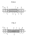
- FIG. 6 is a cross-sectional view of a stacked structure in which two semiconductor devices are stacked each of which has a semiconductor chip connected to an interposer by the wire bonding method as shown in FIG. 3;
- FIG. 7 is a cross-sectional view of a stacked structure in which two semiconductor devices are stacked each of which has a semiconductor chip connected to an interposer by the flip chip bonding method as shown in FIG. 4;
- FIG. 8 is a cross-sectional view of a part of an example of a part of a stacked structure of the semiconductor devices shown in FIG. 4 :
- FIG. 9 is a cross-sectional view of an example of a part of a stacked structure of the semiconductor devices shown in FIG. 4;
- FIG. 10 is a cross-sectional view of a part of a stacked structure of the semiconductor devices according to the present embodiment in which the number of electrodes of an upper semiconductor device is larger than the number of electrodes of a lower semiconductor device;
- FIG. 11 is a cross sectional view of a ball pad having a convex upper surface
- FIG. 12 a cross-sectional view of a semiconductor device according to the second embodiment of the present invention in which a semiconductor chip is mounted by a wire bonding method
- FIG. 13 is a cross-sectional view of a semiconductor device according to the second embodiment of the present invention in which a semiconductor chip is mounted by a flip chip mounting method;
- FIG. 14 is a cross-sectional view of a stacked structure in which two semiconductor devices are stacked each of which has a semiconductor chip connected to the interposer by the wire bonding method as shown in FIG. 12;
- FIG. 15 is a cross-sectional view of a stacked structure in which two semiconductor devices are stacked each of which has a semiconductor chip connected to the interposer by the flip chip bonding method as shown in FIG. 13;
- FIG. 16 is a cross-sectional view of a semiconductor device according to the third embodiment of the present invention in which two semiconductor chips are provided in a stacked relationship and the lower semiconductor chip is connected by a wire bonding method;
- FIG. 17 is a cross-sectional view of a semiconductor device according to the third embodiment of the present invention in which two semiconductor chips are provided in a stacked relationship and the lower semiconductor chip is connected by a flip chip bonding method;
- FIG. 18 is a cross-sectional view of a semiconductor device according to a fourth embodiment of the present invention.
- FIG. 19 is a cross-sectional view of a semiconductor device according to a fifth embodiment of the present invention.
- FIG. 20 is a cross-sectional view of a variation of the semiconductor device according to the fifth embodiment of the present invention.
- FIGS. 21A and 21B are illustrations showing the stacked structures of variations of the semiconductor devices shown in FIGS. 19 and 20;
- FIG. 22 is an illustration showing a process of mounting semiconductor chips to an interposer
- FIG. 23 is an illustration showing a process of bonding a semiconductor chip by a wire bonding method to the interposer having another semiconductor chip mounted thereon;
- FIG. 24A is a side view of the interposer for explaining a method to eliminate a problem caused by the warp of the interposer;
- FIG. 24B is a plan view of the interposer shown in FIG. 24A;
- FIG. 25 is a cross-sectional view of a mold die for encapsulation
- FIG. 26 is a plan view of an interior of the mold die shown in FIG. 25;
- FIG. 27 is an illustration for explaining a cutting process for cutting the interposer
- FIG. 28 is an illustration of the semiconductor device according to the fifth embodiment of the present invention in a state in which the semiconductor device is mounted on a substrate;
- FIG. 29 is an illustration of a semiconductor device having resist layers (insulating layers) provided along the boundary of the seal resin;
- FIG. 30 is an illustration of a stacked structure of semiconductor devices in which a resist layer is used for positioning the semiconductor devices
- FIG. 31 is an illustration of stacked structures in which two semiconductor chips are stacked.
- FIG. 32 is an illustration of stacked structures in which three semiconductor chips are stacked.
- FIG. 33 is an illustration of stacked structures in which four semiconductor chips are stacked.
- FIG. 34 is a perspective view of parts of a stacking apparatus used for stacking the semiconductor devices shown in FIG. 3;
- FIG. 35 is a side view of a semiconductor device placed on a carrier stage
- FIG. 36 is a perspective view of a flux supply unit and a transfer head
- FIG. 37 is a perspective view of a carrier stage and the transfer head
- FIG. 38 is a perspective view of the transfer head viewed from a bottom side
- FIGS. 39A is a cross-sectional view of a part of the transfer head having a flux applying part having a flat surface
- FIG. 39B is a cross-sectional view of a part of the transfer head having a flux applying part having a tapered surface
- FIG. 39C is a cross-sectional view of a part of the transfer head having a flux applying part having a concave surface
- FIG. 40 is a side view of the semiconductor device whose solder balls are-provided with flux
- FIG. 41 is a perspective view of the semiconductor devices placed on a package supply table
- FIG. 42 is a perspective view of a camera unit recognizing positions of the semiconductor devices
- FIG. 43 is a perspective view showing a stack head stacking the semiconductor devices
- FIG. 44 is a side view of the semiconductor devices in a stacked state
- FIG. 45 is an illustration for explaining a method of shaping a solder ball
- FIG. 46 is a cross-sectional view of a positioning jig for positioning the semiconductor devices.
- FIG. 47 is a cross-sectional view of the positioning jig fixed by clip members
- FIG. 48 is a perspective view of parts of a stacking apparatus used for stacking the semiconductor devices.
- FIG. 49 is a side view of the semiconductor device attached to a carrier stage
- FIG. 50 is a perspective view of the flux applying part having a flux filing groove
- FIG. 51 is a perspective view showing the semiconductor devices placed on the package supply table and picked up by the stack head;
- FIG. 52 is a perspective view of the flux applying part and the stack head for explaining a process for applying flux to the semiconductor device
- FIG. 53 is a perspective view of a camera unit recognizing positions of the semiconductor devices
- FIG. 54 is a perspective view showing a stack head stacking the semiconductor devices.
- FIG. 55 is a side view of the semiconductor devices in a stacked state.
- FIG. 3 is a cross-sectional view of a semiconductor device 40 according to the first embodiment of the present invention.
- the semiconductor device 40 is a fan-out type semiconductor chip in which a semiconductor chip 3 is wire bonded.
- the semiconductor chip 3 is mounted on the wiring surface of the interposer 1 , which is a oneside wiring substrate.
- the interposer 1 is formed of an organic material substrate such as a polyamide tap substrate, a glass-epoxy substrate or a polycarbonate substrate.
- the semiconductor chip 3 is fixed to the interposer 1 by the die bonding material 11 .
- the semiconductor chip 3 is wire bonded by the Au wires 4 to the bonding pads 5 formed on the interposer 1 . That is, semiconductor chip 3 is electrically connected to the bonding pads 5 by the Au wires 4 .
- the bonding pads 5 are connected to the ball pads 8 by wiring patterns.
- the surface of the ball pads 8 are covered by a solder resist 10 except for portions to be provided with the solder balls 7 .
- the solder balls 7 are provided to the ball pads 8 on the side of the surface on which the semiconductor chip 3 in mounted.
- the through holes (VIA holes) 9 are formed in the interposer so that the through holes 9 extends trough the interposer 1 from the surface opposite to the surface on which the semiconductor chip 3 is mounted to the back surfaces of the ball pads 8 . Accordingly,the back surfaces of the ball pads 8 are exposed within the respective through holes 9 .
- the size of each of the through holes 9 is set so that an exposed area of each of the ball pad 8 is sufficient to connect the solder ball 7 .
- the solder balls 7 can be provided onto the ball mounting areas of the ball pads 8 . That is, the solder balls 7 are arranged around the semiconductor chip 3 on the surface of the interposer on which the semiconductor chip 3 is mounted.
- the semiconductor chip 3 is a type of a small thickness so that the height of the seal resin 2 from the ball pads 8 is smaller than the height of the solder balls from the ball pads 8 . That is, the solder balls 7 are set higher than the seal resin 2 so that a semiconductor device having the same structure can be easily mounted on the semiconductor device 40 .
- it is effective to use a liquefied resin for the encapsulation.
- use of a vacuum printing apparatus may also effective to achieve a lower and uniform height of the seal resin 2 .
- FIG. 4 is a cross-sectional view of a semiconductor device according to the first embodiment of the present invention in which the semiconductor chip 3 is mounted by a flip chip mounting method.
- parts that are the same as the parts shown in FIG. 3 are given the same reference numerals, and descriptions thereof will be omitted.
- the height of the seal resin 2 can be further reduced than that shown in FIG. 3 by mounting the semiconductor chip 3 by a flip chip mounting method. That is, electric connection between the semiconductor chip 3 and the interposer 1 is achieved by protruding electrodes 12 provided to the semiconductor chip 3 instead of the Au wires 4 so as to reduce the height of the seal resin 2 .
- the protruding electrodes 12 can be Au bumps or solder bumps.
- the under fill material 11 is filled between the semiconductor chip 3 and the interposer 1 so as to reinforce the connection between the protruding electrodes 12 and the bonding pads 5 . If the under fill material 11 is applied after the formation of the solder balls 7 , the under fill material 11 can be supplied to an area where the solder balls 7 are connected to the ball pads 8 , which results in reinforcing the connection of the solder balls 7 . Thereby, a reliable secondary mounting in which the semiconductor device is mounted to a mounting substrate can be achieved.
- the semiconductor device shown in FIG. 4 is a so-called over-mold type in which the entire semiconductor chip 3 is encapsulated by the seal resin 2 .
- the encapsulation by the seal resin 2 can be omitted. Accordingly, the height which must be smaller than the height of the solder balls 7 can be further reduced. In this case, the height corresponds to the height of the semiconductor chip 3 .
- the semiconductor devices shown in FIGS. 3 and 4 can be manufactured at a low cost by using the interposer having wiring patterns on the single side thereof. Additionally, there is no need to apply plating to an inner surface of each of the through holes 9 , and fine wiring can be achieved.
- FIG. 5 is a plan view of the interposer shown in FIG. 3 for explaining positional relationship between the bonding pads 5 and the ball pads 8 .
- the interposer 1 used for the semiconductor devices according to the present embodiment can be provided with wiring patterns in an area facing the semiconductor chip 3 . Accordingly, the positional relationship between the bonding pads 5 and the ball pads 8 can be freely set, resulting in an effective arrangement of the bonding pads 5 and the ball pads 8 in a small area.
- the interposer 1 may be formed by a tape substrate so as to connect the semiconductor chip 3 to the interposer 1 by a tape automated bonding (TAB) method.
- TAB tape automated bonding
- FIG. 6 is a cross-sectional view of a stacked structure of semiconductor devices in which two semiconductor devices are stacked each of which has a semiconductor chip connected to the interposer by the wire bonding method as shown in FIG. 3 .
- FIG. 7 is a cross-sectional view of a stacked structure of semiconductor devices in which two semiconductor devices are stacked each of which has a semiconductor chip connected to the interposer by the flip chip bonding method as shown in FIG. 4 .
- parts that are the same as the parts shown in FIGS. 3 and 4 are given the same reference numerals, and descriptions thereof will be omitted.
- the solder balls 7 provided in the upper semiconductor device are connected to the ball pads 8 of the lower semiconductor device via the through holes 9 provided in the lower semiconductor device. Since the height of the solder balls 7 is larger than the height of the seal resin 2 , the distance between the interposers 1 of the upper semiconductor device and the lower semiconductor device can be maintained larger than the height of the seal resin 2 by the solder balls 7 . Accordingly, the semiconductor chip 3 of the upper semiconductor device is accommodated in a space formed between the interposers 1 of the lower and-upper semiconductor devices.
- the above-mentioned stacked structure of the semiconductor devices can be achieved by merely connecting the solder balls 7 of the upper semiconductor device to the ball pads 8 of the lower semiconductor device by placing the upper semiconductor device to the lower semiconductor device. Accordingly, the stacked structure can be achieved by a simple operation. Additionally, since the solder balls 7 of the upper semiconductor device are positioned within the respective through holes 9 formed in the interposer 1 of the lower semiconductor device, the upper semiconductor device is automatically positioned relative to the lower semiconductor device.
- FIG. 8 is a cross-sectional view of a semiconductor device that is a variation of the semiconductor device according to the first embodiment of the present invention.
- parts that are the same as the parts shown in FIG. 6 are given the same reference numerals, and descriptions thereof will be omitted.
- each of the through holes 9 is formed in a conical shape so that the opening area is larger than-the bottom.
- the solder balls 7 are easily lead to the center of the through holes 9 , resulting in easy positioning of the upper semiconductor device relative to the lower semiconductor device.
- the shape of each of the through holes 9 is not limited to the conical shape, and the each of the through holes 9 may be tapered or an open end of each of the though holes 9 may be chamfered.
- the size of the land on the mounting substrate be less than 1.5 times the size of the through hole 9 . More preferably, the size of the land is equal to the size of the though hole 9 . In such a case, the connecting areas of the solder ball are equalized, thereby preventing the solder being attracted to one side or preventing the stress being generated in the solder after mounting. Additionally, if a solder ball having a high melting point is used for the solder balls 7 of the upper semiconductor device, the solder balls 7 in the stacked structure are prevented from being remelted when the stacked structure is mounted to a mounting board. Thus, a reliable secondary mounting can be achieved.
- the solder balls 7 are not connected to the interposer 1 of the uppermost semiconductor device. Accordingly, there is no need to provide the through holes 9 in the interposer 1 of the uppermost semiconductor device as shown in FIG. 9, which may reduce the manufacturing cost of the semiconductor devices.
- the interposer 1 of the uppermost semiconductor device has through holes 9 , an electrical connection can be made with the semiconductor devices though the through holes 9 , thereby a semiconductor test such as a conductance test can be easily performed.
- FIG. 10 is a cross-sectional view of a part of a stacked structure of the semiconductor devices according to the present embodiment in which the number of electrodes of the upper semiconductor device is larger than the number of electrodes of the lower semiconductor device.
- parts that are the same as the parts shown in FIG. 6 are given the same reference numerals, and descriptions thereof will be omitted.
- an interposer 1 A of the upper semiconductor device is larger than the interposer 1 of the lower semiconductor device so as to provide a ball pad 8 A to the elongated part of the interposer 1 A in addition to the ball pads 8 .
- a solder ball 7 A is provided to the ball pad 8 A arranged on the periphery of the interposer 1 A of the upper semiconductor device. The solder ball 7 A is not connected to the lower semiconductor device, and is larger than the solder ball 7 .
- the height of the solder ball 7 A is larger than the height of the solder balls 7 so that the lower end of the solder ball 7 A reaches the lower end of each of the solder balls 7 .
- the upper semiconductor device can be directly connected to a mounting board such as a motherboard through the solder ball 7 A without routing the lower semiconductor device.
- the semiconductor chip provided in the upper semiconductor device can be a different size than the semiconductor chip provided in the lower semiconductor device.
- various semiconductor devices can be provided in the stacked structure according to the present invention.
- FIG. 11 is a cross-sectional view of an example of a ball pads in the though hole in the semiconductor devices according to the first embodiment of the present invention.
- the ball pad 8 B shown in FIG. 11 has a convex upper surface to which the solder ball 7 of the upper semiconductor device is connected.
- the contact area between the ball pad 8 B and the solder ball 7 is increased, resulting in a reliable connection of the solder ball 7 to the ball pad 8 B.
- the semiconductor chips provided in the semiconductor devices in the stacked structure may be the same kind of chip or different kinds of chips.
- FIG. 12 is a cross-sectional view of a semiconductor device according to the second embodiment of the present invention in which a semiconductor chip is mounted by a wire bonding method.
- FIG. 13 is a cross-sectional view of a semiconductor device according to the second embodiment of the present invention in which a semiconductor chip is mounted by a flip chip mounting method.
- parts that are the same as the parts shown in FIGS. 3 and 4 are given the same reference numerals, and descriptions thereof will be omitted.
- the pars of the semiconductor device according to the second embodiment of the present invention are basically the same as the parts of the semiconductor device according to the above-mentioned first embodiment, and, thus, descriptions will be give of only the differences therebetween.
- the solder balls 7 are provided on the side of the semiconductor chip 3 , that is, on the side of the wiring patterns. Additionally, the height of the seal resin is smaller than the solder balls 7 . Accordingly, the semiconductor chip 3 and the solder balls are provided on the same side of the interposer 1 , and the through holes 9 are provided on the opposite side of the interposer 1 .
- the solder balls 7 are provided on the side opposite to the side of the interposer 1 on which the semiconductor chip 3 is mounted. That is, the solder balls 7 are formed on the ball pads 8 exposed in the through holes 9 . Accordingly, the solder balls 7 protrude from the surface opposite to the surface on which the semiconductor chip 3 is mounted.
- the height of the seal resin 2 is smaller than the height of the solder balls 7 . That is, since the height of the solder balls 7 is larger than the height of the seal resin 2 , the seal resin 2 can be accommodated in a space between the interposers of the upper and lower semiconductor devices when the semiconductor devices according to the present embodiment are stacked as described later.
- the interposer 1 may be formed by a tape substrate so as to connect the semiconductor chip 3 to the interposer 1 by a tape automated.bonding (TAB) method.
- TAB tape automated.bonding
- FIG. 14 is a cross-sectional view of a stacked structure in which two semiconductor devices are stacked each of which has a semiconductor chip connected to the interposer by the wire bonding method as shown in FIG. 12 .
- FIG. 15 is a cross-sectional view of a stacked structure in which two semiconductor devices are stacked each of which has a semiconductor chip connected to the interposer by the flip chip bonding method as shown in FIG. 13 .
- parts that are the same as the parts shown in FIGS. 12 and 13 are given the same reference numerals, and descriptions thereof will be omitted.
- the solder balls 7 provided in the upper semiconductor device are connected to the ball pads 8 of the lower semiconductor device via the through holes 9 provided in the upper semiconductor device. Since the height of the solder balls 7 is larger than the height of the seal resin 2 , the distance between the interposers 1 of the upper semiconductor device and the lower semiconductor device can be maintained larger than the height of the seal resin 2 by the solder balls 7 . Accordingly, the semiconductor chip 3 of the lower semiconductor device is accommodated in a space formed between the interposers 1 of the lower and upper semiconductor devices.
- the above-mentioned stacked structure of the semiconductor devices can be achieved by merely connecting the solder balls 7 of the upper semiconductor device to the ball pads 8 of the lower semiconductor device by placing the upper semiconductor device to the lower semiconductor device. Accordingly, the stacked structure of the semiconductor devices can be achieved by a simple operation.
- the semiconductor chips provided in the semiconductor devices in the stacked structure may be the same kind of chip or different kinds of chips. Additionally, although two semiconductor devices are stacked in the above-mentioned embodiment, more than three semiconductor chips can be stacked in the same manner.
- FIG. 16 is a cross-sectional view of a semiconductor device according to the third embodiment of the present invention in which two semiconductor chips are provided in a stacked relationship and the lower semiconductor chip is connected by a wire bonding method.
- FIG. 17 is a cross-sectional view of a semiconductor device according to the third embodiment of the present invention in which two semiconductor chips are provided in a stacked relationship and the lower semiconductor chip is connected by a flip chip bonding method.
- parts that are the same as the parts shown in FIGS. 3 and 4 are given the same reference numerals, and descriptions thereof will be omitted.
- the semiconductor device according to the third embodiment of the present invention has the same structure as the semiconductor device according to the first embodiment of the present invention except for an additional semiconductor chip 3 A mounted on the semiconductor chip 3 .
- the semiconductor chip 3 A is encapsulated by the seal resin 2 together with the semiconductor chip 3 .
- the semiconductor chip 3 A smaller than the semiconductor chip 3 is stacked on the semiconductor chip 3 via a buffer material 13 interposed therebetween. Both the semiconductor chip 3 and the semiconductor chip 3 A are connected to the bonding pads 5 of the interposer 1 by the Au wires 4 , and are encapsulated by the seal resin 2 . Similar to the semiconductor device according to the first embodiment of the present invention, the height of the seal resin 2 is set to be smaller than the height of the solder balls 7 B. Accordingly, a plurality of semiconductor devices according to the present embodiment can also be connected in a stacked relationship.
- the semiconductor chip 3 is connected to the interposer 1 by a flip chip bonding method.
- Other structures are the same as the semiconductor device shown in FIG. 16 .
- the semiconductor chip 3 may be connected by a TAB method. Additionally, two semiconductor chips are stacked in the semiconductor devices shown in FIGS. 16 and 17, more than three semiconductor chips may be stacked and encapsulated by the seal resin 2 if the height of the solder ball 7 B can be larger than the seal resin 2 .
- FIG. 18 is a cross-sectional view of a semiconductor device according to the fourth embodiment of the present invention.
- parts that are the same as the parts shown in FIG. 12 are given the same reference numerals, and descriptions thereof will be omitted.
- the semiconductor device according to the fourth embodiment of the present invention has the same structure as the semiconductor device according to the second embodiment of the present invention except for an additional semiconductor chip 3 A mounted on the semiconductor chip 3 .
- the semiconductor chip 3 A is encapsulated by the seal resin 2 together with the semiconductor chip 3 .
- the semiconductor chip 3 A smaller than the semiconductor chip 3 is stacked on the semiconductor chip 3 via a buffer material 13 interposed therebetween. Both the semiconductor chip 3 and the semiconductor chip 3 A are connected to the bonding pads 5 of the interposer 1 by the Au wires 4 , and are encapsulated by the seal resin 2 . Similar to the semiconductor device according to the second embodiment of the present invention, the height of the seal resin 2 is set to be smaller than the height of the solder balls 7 B. Accordingly, a plurality of semiconductor devices according to the present embodiment can also be connected in a stacked relationship.
- the semiconductor chip 3 is connected to the interposer 1 by a wire bonding method.
- the semiconductor chip 3 may be connected to the interposer 1 by a flip chip bonding method.
- the semiconductor chip 3 may be connected by a TAB method.
- two semiconductor chips are stacked in the semiconductor devices shown in FIG. 18, more than three semiconductor chips may be stacked and encapsulated by the seal resin 2 if the height of the solder ball 7 B can be larger than the seal resin 2 .
- FIG. 19 is a cross-sectional view of a semiconductor device according to the fifth embodiment of the present invention.
- parts that are the same as the parts shown in FIG. 3 are given the same reference numerals, and descriptions thereof will be omitted.
- an interposer 21 is used.
- the interposer 21 has wining patterns on both sides. Accordingly, the bonding pads 5 and the ball pads 8 are provided on each side of the interposer 21 , and the semiconductor chip 3 is mounted on each side of the interposer 21 and is encapsulated by the seal resin 2 .
- the ball pads 8 or the bonding pads 5 formed on one side of the interposer 21 are electrically connected to the ball pads 8 or the bonding pads 5 formed on the opposite side of the interposer 21 via VIA holes 22 .
- the VIA holes extend through the interposer 21 , and the inner wall are of the VIA holes 22 are plated so as to electrically connect the ball pads 8 or the bonding pads 5 formed on both sides of the interposer 21 .
- Solder balls 7 C are provided on the ball pads formed on one of the sides of the interposer 21 .
- the height of the solder balls 7 C is more than twice the height of the seal resin 2 so that a plurality of semiconductor chips can be stacked. That is, when the semiconductor devices according to the present embodiment are connected in a stacked state, the solder balls 7 C of the upper semiconductor device are connected to the ball pads 8 of the lower semiconductor device.
- the seal resin 2 of the upper semiconductor device and the seal resin 2 of the lower semiconductor device are situated between the interposer 21 of the upper semiconductor device and the interposer 21 of the lower semiconductor device. Accordingly, the height of the solder balls 7 C must be twice the height of the seal resin 2 .
- the lowermost semiconductor device among a plurality of semiconductor devices which are stacked one on another is not necessarily provided with the solder balls 7 C having a large size. That is, the lowermost semiconductor device can be provided with the solder balls 7 having a height larger than the height of the seal resin 2 of the lower semiconductor device.
- the semiconductor chip of the semiconductor device according to the present embodiment may be connected to the interposer by a flip chip bonding method or a TAB method.
- FIGS. 21A and 21B are illustrations showing the stacked structures of variations of the semiconductor devices shown in FIGS. 19 and 20.
- portions other than the portion in which the bonding wires (Au wires) 4 are encapsulated are set to be lower than the seal resin 2 .
- the position of the semiconductor chip 3 of the upper semiconductor device is offset from the position of the semiconductor chip 3 of the lower semiconductor device so that the portions of the encapsulated bonding wire of the upper and lower semiconductor devices do not overlap with each other. That is, the height of the stacked structure is reduced by reducing the distance between the interposer of the upper and lower semiconductor devices by offsetting the encapsulated bonding wire portions since the portions of the bonding wire are the highest portion in the encapsulated potions.
- positioning of the semiconductor devices relative to each other can be performed by fitting the encapsulated bonding wire portion of one semiconductor device to the encapsulated bonding wire portion of the other semiconductor device.
- FIG. 22 is an illustration of a process of mounting semiconductor chips to the interposer 21 .
- semiconductor chips 3 - 1 and 3 - 2 are mounted on each sides of the interposer 21 , respectively. Accordingly, for example, when mounting the semiconductor chip 3 - 1 onto the side of the interposer 21 opposite to the side on which the semiconductor chip 3 - 2 is mounted, the interposer 21 is tuned over and placed on a jig 21 as shown in FIG. 22 . Since the semiconductor chip 3 - 2 is mounted on the lower side of the interposer 21 , the jig has a m recessed portion to accommodate the semiconductor chip 3 - 2 .
- a damper material 31 is provided under the semiconductor chip 3 - 2 so as to support the semiconductor chip 3 - 2 so that interposer 21 is prevented from warping due to a load applied to the semiconductor chip 3 - 1 when mounting the semiconductor chip 3 - 1 to the interposer 21 .
- the damper material 31 be made of an elastic material having a heat resistance such as NBR, silicon rubber or fluorocarbon rubber.
- FIG. 23 is an illustration showing a process of bonding the semiconductor chip 3 - 1 by a wire bonding method to the interposer 21 having the semiconductor chip 3 - 2 mounted thereon.
- a load is applied to the interposer 21 by a wire bonder. Since the interposer 21 is made of a thin substrate, the interposer 21 may warp when a load is applied to the interposer in a state in which only the periphery of the interposer 21 is supported. That is, the center portion of the interposer 21 is depressed downward, which may result in incomplete bonding.
- the wire bonding portions of the upper semiconductor device are offset from the wire bonding portions of the lower semiconductor device. More specifically, the bonding positions of the lower semiconductor chip 3 - 2 are located inside of the bonding positions of the upper semiconductor chip 3 - 1 so that the bonding portions of the interposer 21 are supported by the upper surface of the jig 30 as shown in FIG. 23 when bonding the upper semiconductor chip 3 - 1 , thereby receiving the load of the wire bonder by the jig 30 . Therefore, the interposer 21 does not warp when the upper semiconductor chip 3 - 1 is bonded to the interposer 21 .
- FIG. 24A is a side view of the interposer for explaining a method to eliminate a problem caused by the warp of the interposer.
- FIG. 24B is a plan view of the interposer shown in FIG. 24 A.
- pressing members 32 are pressed against the interposer 21 at portions where the wire bonding is not applied. That is, the interposer 21 is intentionally warped so that a certain level of tension force is generated in the interposer 21 .
- the interposer 21 does not warp further. Thereby, the wire bonding can be normally performed.
- a supporting member may be provided under the interposer 21 at portions where the pressing members 32 are pressed so that the interposer 21 is held between the pressing members 32 and the supporting member.
- FIG. 25 is a cross-sectional view of a mold die for encapsulation.
- FIG. 26 is a plan view of an interior of the mold die shown in FIG. 25 .
- the interposer 21 shown in FIG. 25 has a size sufficient for mounting three semiconductor chips on one side thereof, and further has a portion extending toward a runner 34 of the mold die 33 A, 33 B. Accordingly, in order to inject a seal resin to both sides of the interposer 21 , a runner and gate must be provided to-each of the upper and lower mold dies 33 A and 33 B.
- the runner 34 is provided to only the upper mold die 33 A and an opening 21 a is provided to the interposer 21 at a position near the gates 35 A and 35 B so that the seal resin is introduced into both the upper and lower sides of the interposer 21 . That is, a part of the seal resin injected from the runner 34 of the upper mold die 33 A is introduced into the lower side of the interposer 21 through the opening 21 a . The seal resin introduced into both the upper side and the lower side is injected into both the upper and lower mold dies 33 A and 33 B through the gates 35 A and 35 B. respectively, at the same speed. Accordingly, the semiconductor chips mounted on both sides of the interposer 21 can be encapsulated at the same time with a simple structure.
- the size of the interposer must be large, which may results in warp of the interposer 21 within the mold dies 33 A and 33 B.
- warp preventing pins 36 are provided to the mold dies 33 A and 33 B. The warp preventing pins 36 protrude from the inner surface of each of the upper and lower mold dies 33 A and 33 B so as to contact with the interposer 21 from both sides. Accordingly, the interposer 21 is supported by the warp preventing pins 36 so that the interposer 21 is prevented from warping.
- portions indicated by reference numeral 23 in FIG. 26 are portions to which the warp preventing pins 23 contact.
- each of the warp preventing pins 23 be tapered so as to prevent the warp preventing pins 23 from contacting the bonding wires. Additionally, the warp preventing pins 23 are not always provided to both the upper and lower mold dies 33 A and 33 B, and the warp preventing pins 23 may be provided only to the lower mold die 33 B so as to prevent the interposer 21 form warping due to its own weight.
- the thus-formed semiconductor devices are divided into individual semiconductor devices after unnecessary gate burrs are removed.
- the cutting is performed while the semiconductor devices are fixed to an adhesive tape such as a UV tape which can be easily removed.
- an adhesive tape such as a UV tape which can be easily removed.
- the seal resin is provided to both sides of the interposer 21 , the UV tape adheres only to the seal resin and does not adhere to the interposer 21 .
- a portion of the UV tape 37 corresponding to the seal resin 2 is the cut out so that the UV tape 37 can adhere to the interposer 21 , thereby achieving a stable cutting operation.
- portions of the interposer 21 protruding from the seal resin 2 are cut out by punching or laser cutting before cutting the seal resin 2 , and the seal resin 2 is solely cut in the cutting process by adhering the UV tape 37 to only the seal resin 2 .
- the portions of the interposer 21 to be previously removed may be provided with a partially cut line so as to facilitate the removal of the portions of the interposer 21 .
- FIG. 28 is an illustration of the semiconductor device according to the fifth embodiment of the present invention in a state in which the semiconductor device is mounted on a substrate 38 .
- the semiconductor device can be mounted onto the substrate 38 such as a motherboard in a stable state by providing a buffer material 39 between the lower seal resin and the substrate 38 .
- the buffer material 39 has a function to dump an external force applied to the semiconductor device: a function to fix the semiconductor device to the substrate 38 ; and a function to release heat generated in the semiconductor device to the substrate.
- the buffer material 39 shown in FIG. 28 can be applied to a semiconductor chip in which a semiconductor chip is encapsulated on the lower side of the interposer.
- FIG. 29 is an illustration of a semiconductor device having resist layers (insulating layers) provided along the boundary of the seal resin 2 .
- a part where the semiconductor chip is mounted is not provided with the resist layer 10 A, and the resist layer 10 A is provided only to a part where the solder balls 7 are provided.
- the resist layers 10 A are present along the parting lines between the interposer 21 and each of the upper and lower mold dies, and formation of burrs is prevented by the elasticity of the resist layers 10 A.
- the resist layers 10 A reinforce the interposer 21 , which prevents the interposer 21 from warping. Since the resist layers 10 A are not provided in parts where the semiconductor chips are mounted, the height of the semiconductor device can be reduced by the thickness of the resist layers 10 A.
- the semiconductor device according to the fifth embodiment of the present invention is shown in FIG. 29, the structure of the resist layers 10 A can be applicable to the semiconductor devices according to other embodiments of the present invention.
- FIG. 30 is an illustration of a stacked structure of semiconductor devices in which the resist layer is used for positioning the semiconductor devices.
- the resist layer 10 B is not provided to a part where the real resin is provided but provided to a position where the seal resin 2 of the upper semiconductor device is positioned by the resist layer 10 B of the lower semiconductor deice when the semiconductor devices are stacked.
- FIGS. 31 through 33 are illustrations for explaining various stacked structures of semiconductor devices according to the above-mentioned embodiments.
- FIG. 31 is an illustration of a stacked structure in which two semiconductor chips are stacked;
- FIG. 32 is an illustration of a stacked structure in which three semiconductor chips are stacked;
- FIG. 33 is an illustration of a stacked structure in which four semiconductor chips are stacked.
- the number of semiconductor chips is indicated in the leftmost column, and the stacked structures are shown in the second column.
- the number of interposers included in each of the stacked structures is indicated in the third column.
- a type of external terminals is indicated in the fourth and fifth columns. That is, a mounting method applicable to each of the stacked structures is indicated in the fourth and fifth columns.
- a circle ( ⁇ ) indicates that a BGA (ball grid array) is applicable, and a cross (x) indicates that the BGA is not applicable.
- a circle ( ⁇ ) indicates that an LGA (land grid array) is applicable, and a cross (x) indicates that the LGA is not applicable.
- the sixth trough eighth columns indicate a method applicable to connection of the semiconductor chips provided in each of the stacked structures. That is, in the sixth column, a circle ( ⁇ ) indicates that the semiconductor chip can be connected by a wire bonding method, and a cross (x) indicates that the semiconductor chip cannot be connected by the wire bonding method. In the seventh column, a circle ( ⁇ ) indicates that the semiconductor chip can be connected by a flip chip bonding method, and a cross (x) indicates that the semiconductor chip cannot be connected by the flip chip bonding method. In the eighth column, a circle ( ⁇ ) indicates that the semiconductor chip can be connected by a TAB (tape automated bonding) method, and a cross (x) indicates that the semiconductor chip cannot be connected by the TAB method.
- TAB tape automated bonding
- the ninth and tenth columns indicate kinds of semiconductor chips which can be combined in each of the stacked structures. That is, in the ninth column, a circle ( ⁇ ) indicates that the same kind of semiconductor chips can be combined, and a cross (x) indicates that the same kind of semiconductor chips cannot be combined. In the tenth column, a circle ( ⁇ ) indicates that different kinds of semiconductor chips can be combined, and a cross (x) indicates that different kinds of semiconductor devices cannot be combined.
- FIGS. 31 through 33 A description will now be given of a method for stacking the semiconductor devices in the stacked structures shown in FIGS. 31 through 33. In the following description, it is assumed that the semiconductor devices 40 described with reference to FIG. 3 are stacked.
- FIG. 34 is a perspective view of parts of a stacking apparatus used for stacking the semiconductor devices 40 .
- the stacking apparatus shown in FIG. 34 comprises a package supply table 41 , a stack head 42 , a flux supply unit 43 A, a transfer head 44 A and a camera unit 45 .
- the package supply table 41 is used for temporarily place the semiconductor devices 40 which are manufactured by the aforementioned method. That is, in this embodiment, each of the semiconductor devices 40 is placed on the package supply table 41 so that the solder balls 7 face upward.
- the semiconductor devices 40 after being manufactured are conveyed to the stacking apparatus by being accommodated in a conveying tray.
- the semiconductor chips 40 are accommodated in the conveying tray in a state in which the solder balls face downward so as to protect the solder balls 7 .
- the semiconductor chips 40 taken out of the conveying tray are turned upside down and are placed on the package supply table 41 .
- the stack head 42 are movable in three-dimensional directions by a moving apparatus (not shown in the figure) such as a robot. Additionally, an end of the stack head 42 is provided with a suctioning head unit 47 , which is connected to a suctioning apparatus so that the semiconductor chips 40 can be held by suction.
- the flux supply unit 43 A applies a flux 50 to the transfer head 44 A.
- the flux supply unit 43 A has a cylindrical shape, and a top surface thereof has a flat surface having high flatness.
- the flux 50 is squeezed by a squeegee 48 so as to be a predetermined uniform thickness after being applied to the top surface of the flux supply unit 43 A.
- the thickness of the flux 50 can be set to an arbitrary thickness by adjusting a clearance between the squeegee 48 and the flux supply unit 43 A.
- the transfer head 44 A is movable in three-dimensional directions by a moving apparatus (not shown in the figure) such as a robot.
- the flux 50 is transferred from the flux supply unit 43 A to the transfer head 44 A by the lower end of the transfer head 44 A being pressed against the flux 50 provided to the flux supply unit 43 A.
- the camera unit 45 has a camera 51 taking a picture of an upper portion and a camera 52 taking a picture of a lower portion.
- the camera unit 45 is used for positioning each of the semiconductor devices 40 as described later.
- the lower semiconductor device is indicated by reference numeral 40 A
- the upper semiconductor device is indicated by reference numeral 40 B.
- the semiconductor devices are indicated by reference numeral 40 .
- the camera unit 45 comprises the upper camera 45 and the lower camera 52 in an integral form so that, when the semiconductor devices 40 are stacked, an image of the upper semiconductor device 40 B located above and an image of the lower semiconductor device 40 A located under can be simultaneously taken. Accordingly, there is no need to turn over the camera unit as is in a camera unit having a single camera, which results in an efficient positioning of the semiconductor devices 40 .
- one of the semiconductor device 40 A is attached first to a carrier stage 46 A.
- the carrier stage 46 A is a base table when the semiconductor devices 40 A and 40 B are stacked.
- FIG. 35 is a side view of the semiconductor device 40 A placed on the carrier stage 46 A.
- the carrier stage 46 A is provided with attaching groove 49 A used for positioning the semiconductor device 40 A.
- the stack head 42 conveys one of the semiconductor devices 40 from the package supply table 41 to the carrier stage 46 A, and places the semiconductor device 40 within the attaching groove 49 A.
- the semiconductor devices 40 are placed on the package supply table 41 in a state in which the solder balls 7 face upward. Additionally, the stack head 42 holds the semiconductor device 40 by suctioning the surface of the seal resin 2 of the semiconductor device 40 . Accordingly, in a state in which the semiconductor device 40 is attached on the carrier stage 46 A, the semiconductor device 40 is positioned so that solder balls 7 face upward.
- the flux 50 is applied to the transfer. head 44 A.
- the application of the flux 50 can be performed at the same time the semiconductor device 40 A is conveyed.
- the transfer head 44 A is pressed against the flux supply unit 43 A on which the flux 50 is applied as shown in FIG. 36 .
- the flux 50 had been applied to the flux supply unit 43 A with a predetermined uniform thickness. Accordingly, the flux 50 can be applied to the transfer head 44 A by simply pressing the transfer head 44 A against the flux supply unit 43 A.
- the transfer head 44 A having the flux 50 is moved to the carrier stage 46 A. Then, the transfer head 44 A is pressed against the semiconductor device 40 A attached to the carrier stage 46 A. As mentioned above, the semiconductor device 40 A is positioned on the carrier stage 46 A so that the solder balls 7 faces upward. Accordingly, the flux 50 on the transfer head 44 A is transferred onto the solder balls 7 when the transfer head 44 A is pressed against the semiconductor device 40 A.
- the flux 50 on the transfer head 44 A is transferred only to the solder balls 7 , and does not adhere to other parts of the semiconductor device 40 A. A description will new be give of the reason.
- FIG. 38 is a perspective view of the transfer head viewed from the bottom thereof.
- the bottom of the transfer head 44 A is pressed against the flux supply unit 43 A and the semiconductor device 40 A.
- the bottom of the transfer head 44 A is provided with a depression 53 so that the protruding portion surrounding the depression 53 is formed as a flux applying part 54 A.
- the position of the flux applying part 54 A corresponds to the position of the solder balls 7 on the semiconductor device 40 A. Additionally, the position of the depression 53 corresponds to the position of the seal resin 2 of the semiconductor device 40 A. Accordingly, when the bottom of the transfer head 44 A is pressed against the flux supply unit 43 A, the flux 50 adheres only to the flux applying part 54 A, and does not adhere to the interior of the depression 53 .
- the transfer head 44 A having the flux 59 is pressed against the semiconductor device 40 A, the flux 50 is transferred onto only the solder balls 7 as shown in FIG. 40 . Additionally, when the transfer head 44 A is pressed against the semiconductor device 40 A, the seal resin 2 is opposite to the depression 53 of the transfer head 44 A. Accordingly, the flux 50 is prevented from being mistakenly applied to the seal resin 2 .
- a staking process for stacking the semiconductor devices 40 A and 40 B and a reflow process for connecting the solder balls to the ball pads 8 of the semiconductor device 40 B are performed.
- a conductive metal such as solder included in the flux 50 is melted, and a short circuit may occur between adjacent solder balls or adjacent ball pads.
- the flux 50 is applied only to the solder balls 7 , adjacent solder balls or and the adjacent ball pads are prevented from being short circuited, achieving an improved reliability.
- the amount of the flux 50 transferred onto the solder balls 7 is insufficient, a oxidation film may be formed on the solder balls 7 , and incomplete connection may occur between the solder balls 7 and the respective ball pads 8 . It should be noted that the flux 50 has a function to prevent the solder balls 7 from being oxidized during a heating process.
- FIGS. 39A is a cross-sectional view of a part of the transfer head 44 A provided with the flux applying part 54 A having a flat surface 54 A.
- the amount of the flux 50 is not as large as that shown in FIGS. 39B and 39C.
- FIG. 39B is a cross-sectional view of a part of the transfer head 44 A provided with a flux applying part 54 B having a tapered surface.
- FIG. 39C is a cross-sectional view of a part of the transfer head 44 A provided with the flux applying part 54 C having a spherical surface.
- the stack head 42 moves to a position above the package supply table 41 , and then moves down so as to pick up another semiconductor device 40 as the semiconductor device 40 B to be stacked on the semiconductor device 40 A.
- the camera unit 45 moves to a position above the carrier stage 46 A. At this time, the camera unit 45 moves to a position where the lower camera 52 is opposite to the semiconductor device 40 A attached to the carrier stage 46 A.
- the stack head 42 holds and conveys the semiconductor device 40 B to a position opposite to the upper camera 51 of the camera unit 45 .
- the semiconductor device 40 A is positioned on the lower side and the semiconductor device 40 B is positioned on the upper side with the camera unit 45 located therebetween.
- the upper camera 51 can recognize the positions of the ball pads 8 of the semiconductor device 40 B
- the lower camera 52 can recognize the positions of the solder balls 7 of the semiconductor device 40 A.
- the stack head After the recognition of the positions of the ball pads 8 and the solder balls 7 , the stack head places the semiconductor device 40 B on the semiconductor device 40 A so that the ball pads 8 of the semiconductor device 40 B contacts the respective solder balls 7 of the semiconductor device 40 A. Thereby, the semiconductor devices 40 A and 40 B are arranged in the stacked state as shown in FIG. 44 . In this state, since the flux 50 is transferred on the upper portion of each of the solder balls 7 , the flux 50 does not exist between the seal resin 2 of the lower semiconductor device 40 A and the interposer 1 of the upper semiconductor device 40 B.
- the semiconductor devices 40 A and 40 B are temporarily connected to each other by the flux 50 between the solder balls 7 of the semiconductor device 40 A and the ball pads 8 of the semiconductor device 40 B.
- the semiconductor devices 40 A and 40 B are fixed to each other by bonding the solder balls 7 to the ball pads 8 by placing the carrier stage 46 A in a reflow furnace in a state in which the semiconductor devices 40 A and 40 B are stacked.
- FIGS. 45 through 48 are illustrations for explaining variations of the above-mentioned method for stacking semiconductor devices.
- the solder balls 7 are shaped simultaneously with the transfer of the flux 50 to the solder balls 7 . There is dispersion in the size of the solder balls. If the dispersion is large, the solder balls having a larger diameter can be bonded, but the solder balls having a small diameter cannot be bonded.
- the solder balls 7 are leveled by using a transfer head 44 D.
- the transfer had 44 D is made of hard stainless steel.
- the solder balls 7 are pressed by the transfer head 44 D being moved downward when the flux 50 is being transferred onto the solder balls 7 .
- a flat shaped part 7 A is formed in the upper portion of the solder balls 7 . That is, the height of each of the solder balls 7 can be equalized by leveling the solder balls 7 by the transfer head 44 D, thereby preventing occurrence of incomplete connection when the semiconductor devices are stacked.
- the transfer characteristic of the flux 50 is also improved. Further, since the leveling is performed simultaneously with the transfer of the flux 50 , the above-mentioned effects can be achieved without increasing the number of processes for stacking the semiconductor devices.
- each of the semiconductor devices 40 A and 40 B is positioned by using a positioning jig 55 .
- the positioning jig 55 comprises positioning members 55 A, 55 B and 55 C.
- the positioning jigs 55 A, 55 B and 55 C are fixed relative to each other in a stacked arrangement by positioning pins and positioning holes (not shown in the figure).
- the positioning member 55 A is for positioning the semiconductor device 40 A by a positioning opening 59 A formed therein. That is, the positioning opening 59 A accommodates the semiconductor device 40 A.
- the positioning member 55 B is for positioning the semiconductor device 40 B by a positioning opening 59 B formed therein. That is, the positioning opening 59 B accommodates the semiconductor device 40 B in an accurate position relative to the semiconductor device 40 A accommodated in the positioning opening 59 A of the positioning member 55 A.
- the positioning member 55 C is provided on the positioning member 55 B.
- An opening 56 is formed in the positioning member 55 B so that the flux applying part 54 A of the transfer head 44 E can be inserted into the opening 56 .
- each of the semiconductor devices 40 A and 40 B can be accurately positioned relative to each other.
- the semiconductor device 40 A and the semiconductor device 40 B do not move relative to each other during the stacking process, thereby preventing the flux 50 form adhering to portions other than solder balls 7 .
- the positioning jig 55 shown in FIG. 46 is fixed by a clip members 57 so that the semiconductor devices 40 A and 40 B are subjected to a reflow process in a state in which the semiconductor devices 40 A and 40 B are accommodated in the positioning jig 55 that is clipped by the clip members 57 .
- the semiconductor devices 40 A and 40 B are accurately positioned to each other by the positioning jig 55 , and are subjected to the reflow process in a state in which the semiconductor devices 40 A and 40 B are temporarily connected to each other by the flux 50 .
- the relative positions of the semiconductor devices 40 A and 40 B can be maintained while the flux 50 is melted.
- a heating method for connecting the solder balls 7 to the ball pads 8 is not limited to the reflow process, and a block heater method, a laser method or hot-air method can be used.
- FIG. 48 is a perspective view of parts of a stacking apparatus used for stacking the semiconductor devices 40 in the present embodiment.
- parts that are the same as the parts shown in FIG. 34 are given the same reference numerals, and descriptions thereof will be omitted.
- the stacking apparatus shown in FIG. 48 comprises a package supply table 41 , a stack head 42 , a flux supply unit 43 B and a camera unit 45 .
- the stacking apparatus shown in FIG. 48 does not have the transfer head 44 A provided in the stacking apparatus shown in FIG. 34, and, thereby, the structure of the stacking apparatus is simplified.
- the package supply table 41 has the same structure as that shown in FIG. 34 . However, in this embodiment, each of the semiconductor devices 40 is placed on the package supply table 41 in a state in which the solder balls 7 face the package supply table 41 . As mentioned above, the semiconductor devices. 40 are accommodated in the convey tray with the solder balls 7 facing downward.
- each of the semiconductor devices 40 can be placed on the package supply table 41 without being turned over, and, thereby, the semiconductor devices can be easily transferred from the convey tray to the package supply table 41 . Additionally, when the stack head 42 picks up the semiconductor device 40 on the package supply table 41 , the solder balls 7 of the semiconductor device 40 B face downward.
- the flux supply part 43 B in the present embodiment applies the flux 50 directly to the solder balls 7 of the semiconductor device 40 B.
- the lux supply part 43 B has a cylindrical shape, and a flux filling groove 58 is formed on the top surface of the flux supply part 43 B.
- the flux supply part 43 B has square shape when viewed from above so that the solder balls 7 are inserted into the flux filling groove 58 so as to transfer the flux 50 to the solder balls 7 .
- the flux 50 is provided only in the flux filling groove 58 .
- the flux 50 can be filled in the flux filling groove 58 by applying the flux 50 on the top surface of the flux supply part 43 B and squeezing the flux 50 into the flux filling groove 58 by using the squeegee 48 .
- the thickness of the flux 50 can be controlled to be an arbitrary thickness by adjusting the depth of the flux filling groove 58 .
- FIG. 49 is a side view of the semiconductor device 40 A attached to the carrier stage 46 B.
- the carrier stage 46 A is provided with an attaching depression 49 B for positioning the semiconductor device 40 A on the carrier stage 46 B.
- the stack head 42 picks up the semiconductor device 40 A on the package supply table 41 , and conveys the semiconductor device 40 A to the carrier stage 46 B so as to attach the semiconductor device 40 A within the attaching depression 49 B.
- each of the semiconductor devices 40 is placed on the package supply table in a state in which the solder balls 7 face downward.
- the stack head 42 conveys each of the semiconductor devices 40 by suctioning the interposer of each of the semiconductor devices 40 . Accordingly, in a state in which the semiconductor device 40 A is attached to the carrier stage 46 B, the solder balls 7 of the semiconductor device 40 A face downward.
- the flux 50 is applied to the flux applying part 43 B by using the squeegee 48 as shown in FIG. 50 . It should be noted that the application of the flux 50 may be performed simultaneously with the conveyance of the semiconductor device 40 A. After the application of the flux 50 is completed, the stack head 42 moves to a position above the package supply table 41 and moves down so as to hold the semiconductor device 40 B to be stacked on the semiconductor device 40 A as shown in FIG. 51 .
- the stack head 42 conveys the semiconductor device 40 B to a position above the flux filling groove 58 of the flux supply part 43 B, and then moves downward.
- the semiconductor device 40 B is positioned so that the solder balls face downward.
- stack head 42 moves downward, the solder balls 7 are put into the flux 50 filled in the flux filling groove 58 as shown in FIG. 52 .
- the flux 50 is transferred onto the solder balls 7 .
- the flux 50 is transferred onto only the solder balls 70 , and the flux 50 does not adhere to other parts of the semiconductor device 40 A such as the seal resin 2 . That is, the flux 50 is present only in the flux filling groove 58 of the flux supply part 43 B, and the flux filling groove 58 has a configuration corresponding to the arrangement of the solder balls 7 . Additionally, when filling the flux 50 into the flux filling groove 58 , the flux 50 is prevented from remaining on portions other than the flux filing groove 58 .
- the flux 50 is transferred only to the solder balls 7 .
- a short circuit between adjacent solder balls and adjacent ball pads can be prevented, thereby improving a reliability of the stacked structure of the semiconductor devices.
- the stack head 42 conveys the semiconductor device 40 B to a position above the carrier stage 46 B. That is, the semiconductor device 40 B is moved to a position opposite to the semiconductor device 40 A.
- the camera unit 45 moves to a position above the carrier stage 46 A where the lower camera 52 is opposite to the semiconductor device 40 A attached to the carrier stage 46 A.
- the semiconductor device 40 A is positioned on the lower side and the semiconductor device 40 B is positioned on the upper side with the camera unit 45 located therebetween as shown in FIG. 53 . Accordingly, the upper camera 51 can recognize the positions of the ball pads 8 of the semiconductor device 40 B, and the lower camera 52 can recognize the positions of the solder balls 7 of the semiconductor device 40 A.
- the stack head 42 places the semiconductor device 40 B on the semiconductor device 40 A so that the ball pads 8 of the semiconductor device 40 B contacts the respective solder balls 7 of the semiconductor device 40 A. Thereby, the semiconductor devices 40 A and 40 B are arranged in the stacked state as shown in FIG. 55 . In this state, since the flux 50 is transferred onto the upper portion of each of the solder balls 7 , the flux 50 does not exist between the seal resin 2 of the upper semiconductor device 40 B and the interposer 1 of the lower semiconductor device 40 A.
- the semiconductor devices 40 A and 40 B are temporarily connected to each other by the flux 50 between the solder balls 7 of the semiconductor device 40 A and the ball pads 8 of the semiconductor device 40 B.
- the semiconductor devices 40 A and 40 B are fixed to each other by bonding the solder balls 7 to the ball pads 8 by placing the carrier stage 46 A in a reflow furnace in a state in which the semiconductor devices 40 A and 40 B are stacked.
Landscapes
- Wire Bonding (AREA)
- Structures Or Materials For Encapsulating Or Coating Semiconductor Devices Or Solid State Devices (AREA)
- Encapsulation Of And Coatings For Semiconductor Or Solid State Devices (AREA)
Abstract
Description
Claims (3)
Priority Applications (1)
| Application Number | Priority Date | Filing Date | Title |
|---|---|---|---|
| US10/076,580 US6528348B2 (en) | 1999-11-30 | 2002-02-19 | Semiconductor device having protruding electrodes higher than a sealed portion |
Applications Claiming Priority (6)
| Application Number | Priority Date | Filing Date | Title |
|---|---|---|---|
| JP11-340816 | 1999-11-30 | ||
| JP34081699 | 1999-11-30 | ||
| JP2000-068986 | 2000-03-13 | ||
| JP2000068986A JP3798597B2 (en) | 1999-11-30 | 2000-03-13 | Semiconductor device |
| US09/605,687 US6388333B1 (en) | 1999-11-30 | 2000-06-27 | Semiconductor device having protruding electrodes higher than a sealed portion |
| US10/076,580 US6528348B2 (en) | 1999-11-30 | 2002-02-19 | Semiconductor device having protruding electrodes higher than a sealed portion |
Related Parent Applications (1)
| Application Number | Title | Priority Date | Filing Date |
|---|---|---|---|
| US09/605,687 Continuation US6388333B1 (en) | 1999-11-30 | 2000-06-27 | Semiconductor device having protruding electrodes higher than a sealed portion |
Publications (2)
| Publication Number | Publication Date |
|---|---|
| US20020074630A1 US20020074630A1 (en) | 2002-06-20 |
| US6528348B2 true US6528348B2 (en) | 2003-03-04 |
Family
ID=26576805
Family Applications (2)
| Application Number | Title | Priority Date | Filing Date |
|---|---|---|---|
| US09/605,687 Expired - Lifetime US6388333B1 (en) | 1999-11-30 | 2000-06-27 | Semiconductor device having protruding electrodes higher than a sealed portion |
| US10/076,580 Expired - Lifetime US6528348B2 (en) | 1999-11-30 | 2002-02-19 | Semiconductor device having protruding electrodes higher than a sealed portion |
Family Applications Before (1)
| Application Number | Title | Priority Date | Filing Date |
|---|---|---|---|
| US09/605,687 Expired - Lifetime US6388333B1 (en) | 1999-11-30 | 2000-06-27 | Semiconductor device having protruding electrodes higher than a sealed portion |
Country Status (4)
| Country | Link |
|---|---|
| US (2) | US6388333B1 (en) |
| JP (1) | JP3798597B2 (en) |
| KR (1) | KR100553853B1 (en) |
| TW (1) | TW473981B (en) |
Cited By (16)
| Publication number | Priority date | Publication date | Assignee | Title |
|---|---|---|---|---|
| US20030006494A1 (en) * | 2001-07-03 | 2003-01-09 | Lee Sang Ho | Thin profile stackable semiconductor package and method for manufacturing |
| US20040003496A1 (en) * | 2002-02-21 | 2004-01-08 | Intel Corporation | Interposer to couple a microelectronic device package to a circuit board |
| US20040058472A1 (en) * | 2002-09-25 | 2004-03-25 | Shim Jong Bo | Area array semiconductor package and 3-dimensional stack thereof |
| US20040188855A1 (en) * | 2002-04-19 | 2004-09-30 | Fujitsu Limited | Semiconductor device and manufacturing methods thereof |
| US20060138649A1 (en) * | 2002-10-08 | 2006-06-29 | Chippac, Inc. | Semiconductor multi-package module having inverted second package stacked over die-up flip-chip ball grid array (BGA) package |
| US20060202350A1 (en) * | 2005-03-14 | 2006-09-14 | Kabushiki Kaisha Toshiba | Semiconductor device |
| US20070090284A1 (en) * | 2005-10-20 | 2007-04-26 | Ho Mon N | Image sensor package structure |
| US20090056988A1 (en) * | 2000-05-19 | 2009-03-05 | Megica Corporation | Multiple chips bonded to packaging structure with low noise and multiple selectable functions |
| US20090121361A1 (en) * | 2007-07-02 | 2009-05-14 | Spansion Llc | Semiconductor device and method for manufacturing thereof |
| US20090218677A1 (en) * | 2008-03-03 | 2009-09-03 | Micron Technology, Inc. | Board-on-chip type substrates with conductive traces in multiple planes, semiconductor device packages including such substrates, and associated methods |
| US20100224992A1 (en) * | 2009-03-06 | 2010-09-09 | Mcconnelee Paul Alan | System and method for stacked die embedded chip build-up |
| US20110051378A1 (en) * | 2009-08-26 | 2011-03-03 | Taiwan Semiconductor Manufacturing Company, Ltd. | Wafer-Level Molded Structure for Package Assembly |
| US20110121454A1 (en) * | 2009-11-25 | 2011-05-26 | Hynix Semiconductor Inc. | Stack semiconductor package and method for manufacturing the same |
| US8658473B2 (en) | 2012-03-27 | 2014-02-25 | General Electric Company | Ultrathin buried die module and method of manufacturing thereof |
| US20170294423A1 (en) * | 2012-02-02 | 2017-10-12 | Taiwan Semiconductor Manufacturing Co., Ltd. | Interposer frame and method of manufacturing the same |
| US12622329B2 (en) | 2023-05-22 | 2026-05-05 | Taiwan Semiconductor Manufacturing Company, Ltd. | Interposer frame and method of manufacturing the same |
Families Citing this family (167)
| Publication number | Priority date | Publication date | Assignee | Title |
|---|---|---|---|---|
| TW522530B (en) * | 1999-08-02 | 2003-03-01 | Toyo Kohan Co Ltd | Semiconductor package unit |
| JP4780844B2 (en) * | 2001-03-05 | 2011-09-28 | Okiセミコンダクタ株式会社 | Semiconductor device |
| JP2002270762A (en) * | 2001-03-09 | 2002-09-20 | Sony Corp | Semiconductor device |
| SG108245A1 (en) * | 2001-03-30 | 2005-01-28 | Micron Technology Inc | Ball grid array interposer, packages and methods |
| US6888240B2 (en) * | 2001-04-30 | 2005-05-03 | Intel Corporation | High performance, low cost microelectronic circuit package with interposer |
| US6894399B2 (en) | 2001-04-30 | 2005-05-17 | Intel Corporation | Microelectronic device having signal distribution functionality on an interfacial layer thereof |
| US20020167804A1 (en) * | 2001-05-14 | 2002-11-14 | Intel Corporation | Polymeric encapsulation material with fibrous filler for use in microelectronic circuit packaging |
| US7071024B2 (en) * | 2001-05-21 | 2006-07-04 | Intel Corporation | Method for packaging a microelectronic device using on-die bond pad expansion |
| KR100437539B1 (en) * | 2001-06-29 | 2004-06-26 | 주식회사 하이닉스반도체 | Clock synchronization circuit |
| KR20030042819A (en) * | 2001-11-24 | 2003-06-02 | 앰코 테크놀로지 코리아 주식회사 | Semiconductor Package, Stack Package the same & manufacture method the Packages |
| JP3925615B2 (en) * | 2001-07-04 | 2007-06-06 | ソニー株式会社 | Semiconductor module |
| US7605479B2 (en) * | 2001-08-22 | 2009-10-20 | Tessera, Inc. | Stacked chip assembly with encapsulant layer |
| US7183658B2 (en) | 2001-09-05 | 2007-02-27 | Intel Corporation | Low cost microelectronic circuit package |
| JP4695796B2 (en) * | 2001-09-27 | 2011-06-08 | 富士通セミコンダクター株式会社 | Semiconductor device, semiconductor device unit and manufacturing method thereof |
| JP2003264260A (en) * | 2002-03-08 | 2003-09-19 | Toshiba Corp | Semiconductor chip mounting substrate, semiconductor device, semiconductor module, and semiconductor device mounting substrate |
| US20030224581A1 (en) * | 2002-06-03 | 2003-12-04 | Robert Bosch Gmbh | Flip chip packaging process using laser-induced metal bonding technology, system utilizing the method, and device created by the method |
| US6784544B1 (en) * | 2002-06-25 | 2004-08-31 | Micron Technology, Inc. | Semiconductor component having conductors with wire bondable metalization layers |
| US7573136B2 (en) * | 2002-06-27 | 2009-08-11 | Micron Technology, Inc. | Semiconductor device assemblies and packages including multiple semiconductor device components |
| US6906415B2 (en) * | 2002-06-27 | 2005-06-14 | Micron Technology, Inc. | Semiconductor device assemblies and packages including multiple semiconductor devices and methods |
| US7294928B2 (en) * | 2002-09-06 | 2007-11-13 | Tessera, Inc. | Components, methods and assemblies for stacked packages |
| US7166200B2 (en) * | 2002-09-30 | 2007-01-23 | Tokyo Electron Limited | Method and apparatus for an improved upper electrode plate in a plasma processing system |
| WO2004038798A2 (en) * | 2002-10-22 | 2004-05-06 | Unitive International Limited | Stacked electronic structures including offset substrates |
| KR100480437B1 (en) * | 2002-10-24 | 2005-04-07 | 삼성전자주식회사 | Semiconductor chip package stacked module |
| US7253510B2 (en) * | 2003-01-16 | 2007-08-07 | International Business Machines Corporation | Ball grid array package construction with raised solder ball pads |
| JP4110992B2 (en) | 2003-02-07 | 2008-07-02 | セイコーエプソン株式会社 | Semiconductor device, electronic device, electronic apparatus, semiconductor device manufacturing method, and electronic device manufacturing method |
| JP3680839B2 (en) * | 2003-03-18 | 2005-08-10 | セイコーエプソン株式会社 | Semiconductor device and manufacturing method of semiconductor device |
| JP2004281920A (en) * | 2003-03-18 | 2004-10-07 | Seiko Epson Corp | Semiconductor device, electronic device, electronic equipment, method of manufacturing semiconductor device, and method of manufacturing electronic device |
| JP4096774B2 (en) | 2003-03-24 | 2008-06-04 | セイコーエプソン株式会社 | SEMICONDUCTOR DEVICE, ELECTRONIC DEVICE, ELECTRONIC DEVICE, SEMICONDUCTOR DEVICE MANUFACTURING METHOD, AND ELECTRONIC DEVICE MANUFACTURING METHOD |
| JP2004349495A (en) | 2003-03-25 | 2004-12-09 | Seiko Epson Corp | Semiconductor device, electronic device, electronic apparatus, and method of manufacturing semiconductor device |
| JP3786103B2 (en) * | 2003-05-02 | 2006-06-14 | セイコーエプソン株式会社 | SEMICONDUCTOR DEVICE, ELECTRONIC DEVICE, ELECTRONIC DEVICE, AND SEMICONDUCTOR DEVICE MANUFACTURING METHOD |
| CN1295766C (en) * | 2003-05-29 | 2007-01-17 | 财团法人工业技术研究院 | Electronic sealer with three-dimensional stack and assembling method thereof |
| JP3858854B2 (en) | 2003-06-24 | 2006-12-20 | 富士通株式会社 | Multilayer semiconductor device |
| US20040262728A1 (en) * | 2003-06-30 | 2004-12-30 | Sterrett Terry L. | Modular device assemblies |
| KR100592786B1 (en) * | 2003-08-22 | 2006-06-26 | 삼성전자주식회사 | Laminated package and its manufacturing method using surface-mount semiconductor package |
| US7180165B2 (en) * | 2003-09-05 | 2007-02-20 | Sanmina, Sci Corporation | Stackable electronic assembly |
| JP2005129752A (en) * | 2003-10-24 | 2005-05-19 | Seiko Epson Corp | Semiconductor device and manufacturing method thereof, circuit board, and electronic apparatus |
| EP2221865B1 (en) | 2004-01-07 | 2019-05-22 | Nikon Corporation | Stacking apparatus and method for stacking a plurality of wafers |
| JP4291209B2 (en) | 2004-05-20 | 2009-07-08 | エルピーダメモリ株式会社 | Manufacturing method of semiconductor device |
| JP4051570B2 (en) | 2004-05-26 | 2008-02-27 | セイコーエプソン株式会社 | Manufacturing method of semiconductor device |
| US6987314B1 (en) * | 2004-06-08 | 2006-01-17 | Amkor Technology, Inc. | Stackable semiconductor package with solder on pads on which second semiconductor package is stacked |
| US7187068B2 (en) * | 2004-08-11 | 2007-03-06 | Intel Corporation | Methods and apparatuses for providing stacked-die devices |
| KR100688501B1 (en) | 2004-09-10 | 2007-03-02 | 삼성전자주식회사 | Stacked BOC Package with Mirroring Structure and Double-sided Mounted Memory Module |
| US8525314B2 (en) | 2004-11-03 | 2013-09-03 | Tessera, Inc. | Stacked packaging improvements |
| US20060108676A1 (en) * | 2004-11-22 | 2006-05-25 | Punzalan Nelson V Jr | Multi-chip package using an interposer |
| WO2006080082A1 (en) * | 2005-01-28 | 2006-08-03 | Spansion Llc | Layered semiconductor device carrier and layered semiconductor device manufacturing method |
| JP4827556B2 (en) * | 2005-03-18 | 2011-11-30 | キヤノン株式会社 | Stacked semiconductor package |
| US7545031B2 (en) * | 2005-04-11 | 2009-06-09 | Stats Chippac Ltd. | Multipackage module having stacked packages with asymmetrically arranged die and molding |
| JP4308797B2 (en) * | 2005-05-02 | 2009-08-05 | 株式会社アドバンストシステムズジャパン | Circuit board with semiconductor package and socket |
| US7763963B2 (en) * | 2005-05-04 | 2010-07-27 | Stats Chippac Ltd. | Stacked package semiconductor module having packages stacked in a cavity in the module substrate |
| US7746656B2 (en) * | 2005-05-16 | 2010-06-29 | Stats Chippac Ltd. | Offset integrated circuit package-on-package stacking system |
| US7518224B2 (en) * | 2005-05-16 | 2009-04-14 | Stats Chippac Ltd. | Offset integrated circuit package-on-package stacking system |
| US7576995B2 (en) | 2005-11-04 | 2009-08-18 | Entorian Technologies, Lp | Flex circuit apparatus and method for adding capacitance while conserving circuit board surface area |
| US8026611B2 (en) | 2005-12-01 | 2011-09-27 | Tessera, Inc. | Stacked microelectronic packages having at least two stacked microelectronic elements adjacent one another |
| JP4937581B2 (en) * | 2005-12-22 | 2012-05-23 | ルネサスエレクトロニクス株式会社 | Electronic equipment |
| US8058101B2 (en) | 2005-12-23 | 2011-11-15 | Tessera, Inc. | Microelectronic packages and methods therefor |
| US7304382B2 (en) | 2006-01-11 | 2007-12-04 | Staktek Group L.P. | Managed memory component |
| US7605454B2 (en) | 2006-01-11 | 2009-10-20 | Entorian Technologies, Lp | Memory card and method for devising |
| US7508058B2 (en) | 2006-01-11 | 2009-03-24 | Entorian Technologies, Lp | Stacked integrated circuit module |
| US7608920B2 (en) | 2006-01-11 | 2009-10-27 | Entorian Technologies, Lp | Memory card and method for devising |
| US7508069B2 (en) | 2006-01-11 | 2009-03-24 | Entorian Technologies, Lp | Managed memory component |
| JP4764196B2 (en) * | 2006-02-14 | 2011-08-31 | Okiセミコンダクタ株式会社 | Manufacturing method of semiconductor device |
| US7652361B1 (en) * | 2006-03-03 | 2010-01-26 | Amkor Technology, Inc. | Land patterns for a semiconductor stacking structure and method therefor |
| TW200737506A (en) | 2006-03-07 | 2007-10-01 | Sanyo Electric Co | Semiconductor device and manufacturing method of the same |
| JP4654971B2 (en) * | 2006-05-19 | 2011-03-23 | 日立電線株式会社 | Multilayer semiconductor device |
| JP2008016630A (en) * | 2006-07-06 | 2008-01-24 | Matsushita Electric Ind Co Ltd | Printed wiring board and manufacturing method thereof |
| SG139573A1 (en) * | 2006-07-17 | 2008-02-29 | Micron Technology Inc | Microelectronic packages with leadframes, including leadframes configured for stacked die packages, and associated systems and methods |
| CN100539122C (en) * | 2006-07-21 | 2009-09-09 | 日月光半导体制造股份有限公司 | Package of system package |
| US7486525B2 (en) * | 2006-08-04 | 2009-02-03 | International Business Machines Corporation | Temporary chip attach carrier |
| TWI367557B (en) | 2006-08-11 | 2012-07-01 | Sanyo Electric Co | Semiconductor device and manufaturing method thereof |
| US7638868B2 (en) * | 2006-08-16 | 2009-12-29 | Tessera, Inc. | Microelectronic package |
| US7468553B2 (en) | 2006-10-20 | 2008-12-23 | Entorian Technologies, Lp | Stackable micropackages and stacked modules |
| KR100885911B1 (en) * | 2006-11-16 | 2009-02-26 | 삼성전자주식회사 | Semiconductor package with improved heat dissipation |
| JP5010247B2 (en) | 2006-11-20 | 2012-08-29 | オンセミコンダクター・トレーディング・リミテッド | Semiconductor device and manufacturing method thereof |
| US7635913B2 (en) * | 2006-12-09 | 2009-12-22 | Stats Chippac Ltd. | Stacked integrated circuit package-in-package system |
| US8163600B2 (en) * | 2006-12-28 | 2012-04-24 | Stats Chippac Ltd. | Bridge stack integrated circuit package-on-package system |
| JP2008198916A (en) * | 2007-02-15 | 2008-08-28 | Spansion Llc | Semiconductor device and manufacturing method thereof |
| JP4751351B2 (en) * | 2007-02-20 | 2011-08-17 | 株式会社東芝 | Semiconductor device and semiconductor module using the same |
| KR100887475B1 (en) * | 2007-02-26 | 2009-03-10 | 주식회사 네패스 | Semiconductor package and manufacturing method |
| US7598523B2 (en) * | 2007-03-19 | 2009-10-06 | Taiwan Semiconductor Manufacturing Company, Ltd. | Test structures for stacking dies having through-silicon vias |
| JP4949114B2 (en) * | 2007-04-11 | 2012-06-06 | 新光電気工業株式会社 | Connection material coating apparatus and semiconductor device manufacturing method |
| US7868441B2 (en) * | 2007-04-13 | 2011-01-11 | Maxim Integrated Products, Inc. | Package on-package secure module having BGA mesh cap |
| US20110024890A1 (en) | 2007-06-29 | 2011-02-03 | Stats Chippac, Ltd. | Stackable Package By Using Internal Stacking Modules |
| SG149726A1 (en) * | 2007-07-24 | 2009-02-27 | Micron Technology Inc | Microelectronic die packages with metal leads, including metal leads for stacked die packages, and associated systems and methods |
| US8299626B2 (en) | 2007-08-16 | 2012-10-30 | Tessera, Inc. | Microelectronic package |
| SG150396A1 (en) | 2007-08-16 | 2009-03-30 | Micron Technology Inc | Microelectronic die packages with leadframes, including leadframe-based interposer for stacked die packages, and associated systems and methods |
| JP2009099750A (en) * | 2007-10-17 | 2009-05-07 | Powertech Technology Inc | Semiconductor package |
| JP2009099749A (en) * | 2007-10-17 | 2009-05-07 | Powertech Technology Inc | Semiconductor package |
| TWI355061B (en) * | 2007-12-06 | 2011-12-21 | Nanya Technology Corp | Stacked-type chip package structure and fabricatio |
| TW200931634A (en) * | 2008-01-10 | 2009-07-16 | Abounion Technology Corp | Multi-channel stacked semiconductor device and method for fabricating the same, and stacking substrate applied to the semiconductor device |
| JP2009206229A (en) * | 2008-02-27 | 2009-09-10 | Furukawa Electric Co Ltd:The | Semiconductor device and its manufacturing method |
| KR20090129791A (en) * | 2008-06-13 | 2009-12-17 | 가부시키가이샤 교토 소프트웨어 리서치 | Multi-value flash memory |
| US7989950B2 (en) | 2008-08-14 | 2011-08-02 | Stats Chippac Ltd. | Integrated circuit packaging system having a cavity |
| US8823160B2 (en) * | 2008-08-22 | 2014-09-02 | Stats Chippac Ltd. | Integrated circuit package system having cavity |
| US8130512B2 (en) * | 2008-11-18 | 2012-03-06 | Stats Chippac Ltd. | Integrated circuit package system and method of package stacking |
| US8518749B2 (en) | 2009-06-22 | 2013-08-27 | Stats Chippac, Ltd. | Semiconductor device and method of forming prefabricated heat spreader frame with embedded semiconductor die |
| KR101061180B1 (en) * | 2009-06-29 | 2011-09-01 | 주식회사 하이닉스반도체 | Semiconductor package |
| US8022526B2 (en) | 2009-08-07 | 2011-09-20 | Advanced Processor Architectures, Llc | Distributed computing |
| US11042211B2 (en) | 2009-08-07 | 2021-06-22 | Advanced Processor Architectures, Llc | Serially connected computing nodes in a distributed computing system |
| US9645603B1 (en) | 2013-09-12 | 2017-05-09 | Advanced Processor Architectures, Llc | System clock distribution in a distributed computing environment |
| US9429983B1 (en) | 2013-09-12 | 2016-08-30 | Advanced Processor Architectures, Llc | System clock distribution in a distributed computing environment |
| JP5644264B2 (en) * | 2009-10-14 | 2014-12-24 | 富士通株式会社 | Semiconductor device |
| US8476775B2 (en) * | 2009-12-17 | 2013-07-02 | Stats Chippac Ltd. | Integrated circuit packaging system with embedded interconnect and method of manufacture thereof |
| JP5544950B2 (en) * | 2010-03-16 | 2014-07-09 | カシオ計算機株式会社 | Semiconductor device manufacturing method and semiconductor device mounting method |
| US9159708B2 (en) | 2010-07-19 | 2015-10-13 | Tessera, Inc. | Stackable molded microelectronic packages with area array unit connectors |
| US8482111B2 (en) | 2010-07-19 | 2013-07-09 | Tessera, Inc. | Stackable molded microelectronic packages |
| US8598695B2 (en) | 2010-07-23 | 2013-12-03 | Tessera, Inc. | Active chip on carrier or laminated chip having microelectronic element embedded therein |
| US8378477B2 (en) * | 2010-09-14 | 2013-02-19 | Stats Chippac Ltd. | Integrated circuit packaging system with film encapsulation and method of manufacture thereof |
| TWI559480B (en) * | 2010-09-15 | 2016-11-21 | 史達晶片有限公司 | Stackable package using internal stacked modules |
| KR101075241B1 (en) | 2010-11-15 | 2011-11-01 | 테세라, 인코포레이티드 | Microelectronic package with terminals in dielectric member |
| US8421203B2 (en) | 2010-11-17 | 2013-04-16 | Stats Chippac Ltd. | Integrated circuit packaging system with foldable substrate and method of manufacture thereof |
| US8372695B2 (en) | 2010-11-19 | 2013-02-12 | Stats Chippac Ltd. | Integrated circuit packaging system with stack interconnect and method of manufacture thereof |
| US8502387B2 (en) | 2010-12-09 | 2013-08-06 | Stats Chippac Ltd. | Integrated circuit packaging system with vertical interconnection and method of manufacture thereof |
| US9093392B2 (en) | 2010-12-10 | 2015-07-28 | Stats Chippac Ltd. | Integrated circuit packaging system with vertical interconnection and method of manufacture thereof |
| US20120146206A1 (en) | 2010-12-13 | 2012-06-14 | Tessera Research Llc | Pin attachment |
| US8618659B2 (en) | 2011-05-03 | 2013-12-31 | Tessera, Inc. | Package-on-package assembly with wire bonds to encapsulation surface |
| KR101128063B1 (en) | 2011-05-03 | 2012-04-23 | 테세라, 인코포레이티드 | Package-on-package assembly with wire bonds to encapsulation surface |
| KR101831692B1 (en) * | 2011-08-17 | 2018-02-26 | 삼성전자주식회사 | Semiconductor Devices, Package Substrates, Semiconductor Packages, Package Stack Structures, and Electronic Systems having Functionally Asymmetric Conductive elements |
| US8872318B2 (en) | 2011-08-24 | 2014-10-28 | Tessera, Inc. | Through interposer wire bond using low CTE interposer with coarse slot apertures |
| KR101774938B1 (en) | 2011-08-31 | 2017-09-06 | 삼성전자 주식회사 | Semiconductor package having supporting plate and method of forming the same |
| US8404520B1 (en) | 2011-10-17 | 2013-03-26 | Invensas Corporation | Package-on-package assembly with wire bond vias |
| US8946757B2 (en) | 2012-02-17 | 2015-02-03 | Invensas Corporation | Heat spreading substrate with embedded interconnects |
| US8372741B1 (en) | 2012-02-24 | 2013-02-12 | Invensas Corporation | Method for package-on-package assembly with wire bonds to encapsulation surface |
| US9349706B2 (en) | 2012-02-24 | 2016-05-24 | Invensas Corporation | Method for package-on-package assembly with wire bonds to encapsulation surface |
| US8835228B2 (en) | 2012-05-22 | 2014-09-16 | Invensas Corporation | Substrate-less stackable package with wire-bond interconnect |
| US9391008B2 (en) | 2012-07-31 | 2016-07-12 | Invensas Corporation | Reconstituted wafer-level package DRAM |
| US9502390B2 (en) | 2012-08-03 | 2016-11-22 | Invensas Corporation | BVA interposer |
| US8975738B2 (en) | 2012-11-12 | 2015-03-10 | Invensas Corporation | Structure for microelectronic packaging with terminals on dielectric mass |
| US8878353B2 (en) | 2012-12-20 | 2014-11-04 | Invensas Corporation | Structure for microelectronic packaging with bond elements to encapsulation surface |
| US9136254B2 (en) | 2013-02-01 | 2015-09-15 | Invensas Corporation | Microelectronic package having wire bond vias and stiffening layer |
| US9034696B2 (en) | 2013-07-15 | 2015-05-19 | Invensas Corporation | Microelectronic assemblies having reinforcing collars on connectors extending through encapsulation |
| US8883563B1 (en) | 2013-07-15 | 2014-11-11 | Invensas Corporation | Fabrication of microelectronic assemblies having stack terminals coupled by connectors extending through encapsulation |
| US9023691B2 (en) | 2013-07-15 | 2015-05-05 | Invensas Corporation | Microelectronic assemblies with stack terminals coupled by connectors extending through encapsulation |
| US9167710B2 (en) | 2013-08-07 | 2015-10-20 | Invensas Corporation | Embedded packaging with preformed vias |
| US9685365B2 (en) | 2013-08-08 | 2017-06-20 | Invensas Corporation | Method of forming a wire bond having a free end |
| US20150076714A1 (en) | 2013-09-16 | 2015-03-19 | Invensas Corporation | Microelectronic element with bond elements to encapsulation surface |
| US9082753B2 (en) | 2013-11-12 | 2015-07-14 | Invensas Corporation | Severing bond wire by kinking and twisting |
| US9087815B2 (en) | 2013-11-12 | 2015-07-21 | Invensas Corporation | Off substrate kinking of bond wire |
| US9263394B2 (en) | 2013-11-22 | 2016-02-16 | Invensas Corporation | Multiple bond via arrays of different wire heights on a same substrate |
| US9583456B2 (en) | 2013-11-22 | 2017-02-28 | Invensas Corporation | Multiple bond via arrays of different wire heights on a same substrate |
| US9379074B2 (en) | 2013-11-22 | 2016-06-28 | Invensas Corporation | Die stacks with one or more bond via arrays of wire bond wires and with one or more arrays of bump interconnects |
| JP6335513B2 (en) | 2014-01-10 | 2018-05-30 | 新光電気工業株式会社 | Semiconductor device and method for manufacturing semiconductor device |
| US9583411B2 (en) | 2014-01-17 | 2017-02-28 | Invensas Corporation | Fine pitch BVA using reconstituted wafer with area array accessible for testing |
| US9214454B2 (en) | 2014-03-31 | 2015-12-15 | Invensas Corporation | Batch process fabrication of package-on-package microelectronic assemblies |
| US10381326B2 (en) | 2014-05-28 | 2019-08-13 | Invensas Corporation | Structure and method for integrated circuits packaging with increased density |
| US9646917B2 (en) | 2014-05-29 | 2017-05-09 | Invensas Corporation | Low CTE component with wire bond interconnects |
| US9412714B2 (en) | 2014-05-30 | 2016-08-09 | Invensas Corporation | Wire bond support structure and microelectronic package including wire bonds therefrom |
| US10446728B2 (en) * | 2014-10-31 | 2019-10-15 | eLux, Inc. | Pick-and remove system and method for emissive display repair |
| KR102341755B1 (en) | 2014-11-10 | 2021-12-23 | 삼성전자주식회사 | Semiconductor packages and methods for fabricating the same |
| US9735084B2 (en) | 2014-12-11 | 2017-08-15 | Invensas Corporation | Bond via array for thermal conductivity |
| US9888579B2 (en) | 2015-03-05 | 2018-02-06 | Invensas Corporation | Pressing of wire bond wire tips to provide bent-over tips |
| US9502372B1 (en) | 2015-04-30 | 2016-11-22 | Invensas Corporation | Wafer-level packaging using wire bond wires in place of a redistribution layer |
| US9761554B2 (en) | 2015-05-07 | 2017-09-12 | Invensas Corporation | Ball bonding metal wire bond wires to metal pads |
| US10490528B2 (en) | 2015-10-12 | 2019-11-26 | Invensas Corporation | Embedded wire bond wires |
| US9490222B1 (en) | 2015-10-12 | 2016-11-08 | Invensas Corporation | Wire bond wires for interference shielding |
| US10332854B2 (en) | 2015-10-23 | 2019-06-25 | Invensas Corporation | Anchoring structure of fine pitch bva |
| US10181457B2 (en) | 2015-10-26 | 2019-01-15 | Invensas Corporation | Microelectronic package for wafer-level chip scale packaging with fan-out |
| US10043779B2 (en) | 2015-11-17 | 2018-08-07 | Invensas Corporation | Packaged microelectronic device for a package-on-package device |
| US9659848B1 (en) | 2015-11-18 | 2017-05-23 | Invensas Corporation | Stiffened wires for offset BVA |
| US9984992B2 (en) | 2015-12-30 | 2018-05-29 | Invensas Corporation | Embedded wire bond wires for vertical integration with separate surface mount and wire bond mounting surfaces |
| US9659911B1 (en) * | 2016-04-20 | 2017-05-23 | Powertech Technology Inc. | Package structure and manufacturing method thereof |
| US12094811B2 (en) | 2016-04-29 | 2024-09-17 | Kulicke And Soffa Industries, Inc. | Connecting electronic components to substrates |
| US9935075B2 (en) | 2016-07-29 | 2018-04-03 | Invensas Corporation | Wire bonding method and apparatus for electromagnetic interference shielding |
| US10141276B2 (en) * | 2016-09-09 | 2018-11-27 | Powertech Technology Inc. | Semiconductor package structure and manufacturing method thereof |
| US10299368B2 (en) | 2016-12-21 | 2019-05-21 | Invensas Corporation | Surface integrated waveguides and circuit structures therefor |
| KR101933421B1 (en) * | 2017-10-27 | 2018-12-28 | 삼성전기 주식회사 | Fan-out semiconductor package module |
| US10741498B2 (en) * | 2018-07-12 | 2020-08-11 | Samsung Electronics Co., Ltd. | Semiconductor package |
| US11869823B2 (en) * | 2019-11-08 | 2024-01-09 | Octavo Systems Llc | System in a package modifications |
Citations (5)
| Publication number | Priority date | Publication date | Assignee | Title |
|---|---|---|---|---|
| JPH08236694A (en) | 1995-02-24 | 1996-09-13 | Nec Corp | Semiconductor package and manufacturing method thereof |
| US5594275A (en) | 1993-11-18 | 1997-01-14 | Samsung Electronics Co., Ltd. | J-leaded semiconductor package having a plurality of stacked ball grid array packages |
| JPH09148482A (en) | 1995-11-24 | 1997-06-06 | Nec Corp | Semiconductor device |
| US6025648A (en) | 1997-04-17 | 2000-02-15 | Nec Corporation | Shock resistant semiconductor device and method for producing same |
| US6072233A (en) | 1998-05-04 | 2000-06-06 | Micron Technology, Inc. | Stackable ball grid array package |
-
2000
- 2000-03-13 JP JP2000068986A patent/JP3798597B2/en not_active Expired - Fee Related
- 2000-06-23 TW TW089112421A patent/TW473981B/en not_active IP Right Cessation
- 2000-06-27 US US09/605,687 patent/US6388333B1/en not_active Expired - Lifetime
- 2000-07-06 KR KR1020000038655A patent/KR100553853B1/en not_active Expired - Fee Related
-
2002
- 2002-02-19 US US10/076,580 patent/US6528348B2/en not_active Expired - Lifetime
Patent Citations (5)
| Publication number | Priority date | Publication date | Assignee | Title |
|---|---|---|---|---|
| US5594275A (en) | 1993-11-18 | 1997-01-14 | Samsung Electronics Co., Ltd. | J-leaded semiconductor package having a plurality of stacked ball grid array packages |
| JPH08236694A (en) | 1995-02-24 | 1996-09-13 | Nec Corp | Semiconductor package and manufacturing method thereof |
| JPH09148482A (en) | 1995-11-24 | 1997-06-06 | Nec Corp | Semiconductor device |
| US6025648A (en) | 1997-04-17 | 2000-02-15 | Nec Corporation | Shock resistant semiconductor device and method for producing same |
| US6072233A (en) | 1998-05-04 | 2000-06-06 | Micron Technology, Inc. | Stackable ball grid array package |
Cited By (37)
| Publication number | Priority date | Publication date | Assignee | Title |
|---|---|---|---|---|
| US20090056988A1 (en) * | 2000-05-19 | 2009-03-05 | Megica Corporation | Multiple chips bonded to packaging structure with low noise and multiple selectable functions |
| US8148806B2 (en) * | 2000-05-19 | 2012-04-03 | Megica Corporation | Multiple chips bonded to packaging structure with low noise and multiple selectable functions |
| US20090057919A1 (en) * | 2000-05-19 | 2009-03-05 | Megica Corporation | Multiple chips bonded to packaging structure with low noise and multiple selectable functions |
| US20030006494A1 (en) * | 2001-07-03 | 2003-01-09 | Lee Sang Ho | Thin profile stackable semiconductor package and method for manufacturing |
| US20040003496A1 (en) * | 2002-02-21 | 2004-01-08 | Intel Corporation | Interposer to couple a microelectronic device package to a circuit board |
| US6960827B2 (en) * | 2002-04-19 | 2005-11-01 | Fujitsu Limited | Semiconductor device and manufacturing method thereof |
| US20040188855A1 (en) * | 2002-04-19 | 2004-09-30 | Fujitsu Limited | Semiconductor device and manufacturing methods thereof |
| US6847109B2 (en) * | 2002-09-25 | 2005-01-25 | Samsung Electronics Co., Ltd. | Area array semiconductor package and 3-dimensional stack thereof |
| US20040058472A1 (en) * | 2002-09-25 | 2004-03-25 | Shim Jong Bo | Area array semiconductor package and 3-dimensional stack thereof |
| US20060138649A1 (en) * | 2002-10-08 | 2006-06-29 | Chippac, Inc. | Semiconductor multi-package module having inverted second package stacked over die-up flip-chip ball grid array (BGA) package |
| US20060202350A1 (en) * | 2005-03-14 | 2006-09-14 | Kabushiki Kaisha Toshiba | Semiconductor device |
| US7397132B2 (en) | 2005-03-14 | 2008-07-08 | Kabushiki Kaisha Toshiba | Semiconductor device |
| US20070090284A1 (en) * | 2005-10-20 | 2007-04-26 | Ho Mon N | Image sensor package structure |
| US8446015B2 (en) * | 2007-07-02 | 2013-05-21 | Spansion Llc | Semiconductor device and method for manufacturing thereof |
| US20090121361A1 (en) * | 2007-07-02 | 2009-05-14 | Spansion Llc | Semiconductor device and method for manufacturing thereof |
| US20120049362A1 (en) * | 2007-07-02 | 2012-03-01 | Naomi Masuda | Semiconductor device and method for manufacturing thereof |
| US7892892B2 (en) * | 2007-07-02 | 2011-02-22 | Spansion Llc | Semiconductor device and method for manufacturing thereof |
| US8288859B2 (en) | 2008-03-03 | 2012-10-16 | Micron Technology, Inc. | Semiconductor device packages including a semiconductor device and a redistribution element |
| US8486825B2 (en) | 2008-03-03 | 2013-07-16 | Micron Technology, Inc. | Methods of forming semiconductor device packages including a semiconductor device and a redistribution element, methods of forming redistribution elements and methods for packaging semiconductor devices |
| US8030751B2 (en) | 2008-03-03 | 2011-10-04 | Micron Technology, Inc. | Board-on-chip type substrates with conductive traces in multiple planes and semiconductor device packages including such substrates |
| US8749050B2 (en) | 2008-03-03 | 2014-06-10 | Micron Technology, Inc. | Redistribution elements and semiconductor device packages including semiconductor devices and redistribution elements |
| US20090218677A1 (en) * | 2008-03-03 | 2009-09-03 | Micron Technology, Inc. | Board-on-chip type substrates with conductive traces in multiple planes, semiconductor device packages including such substrates, and associated methods |
| US8008125B2 (en) * | 2009-03-06 | 2011-08-30 | General Electric Company | System and method for stacked die embedded chip build-up |
| US20100224992A1 (en) * | 2009-03-06 | 2010-09-09 | Mcconnelee Paul Alan | System and method for stacked die embedded chip build-up |
| US9754917B2 (en) | 2009-08-26 | 2017-09-05 | Taiwan Semiconductor Manufacturing Company, Ltd. | Method of forming wafer-level molded structure for package assembly |
| US20110051378A1 (en) * | 2009-08-26 | 2011-03-03 | Taiwan Semiconductor Manufacturing Company, Ltd. | Wafer-Level Molded Structure for Package Assembly |
| US8743561B2 (en) * | 2009-08-26 | 2014-06-03 | Taiwan Semiconductor Manufacturing Company, Ltd. | Wafer-level molded structure for package assembly |
| US9117939B2 (en) | 2009-08-26 | 2015-08-25 | Taiwan Semiconductor Manufacturing Company, Ltd. | Method of forming wafer-level molded structure for package assembly |
| US20110121454A1 (en) * | 2009-11-25 | 2011-05-26 | Hynix Semiconductor Inc. | Stack semiconductor package and method for manufacturing the same |
| US8164200B2 (en) * | 2009-11-25 | 2012-04-24 | Hynix Semiconductor Inc. | Stack semiconductor package and method for manufacturing the same |
| US20170294423A1 (en) * | 2012-02-02 | 2017-10-12 | Taiwan Semiconductor Manufacturing Co., Ltd. | Interposer frame and method of manufacturing the same |
| US10840224B2 (en) * | 2012-02-02 | 2020-11-17 | Taiwan Semiconductor Manufacturing Co., Ltd. | Interposer frame and method of manufacturing the same |
| US10861836B2 (en) | 2012-02-02 | 2020-12-08 | Taiwan Semiconductor Manufacturing Co., Ltd. | Interposer frame and method of manufacturing the same |
| US11699691B2 (en) | 2012-02-02 | 2023-07-11 | Taiwan Semiconductor Manufacturing Company, Ltd. | Interposer frame and method of manufacturing the same |
| US9236348B2 (en) | 2012-03-27 | 2016-01-12 | General Electric Company | Ultrathin buried die module and method of manufacturing thereof |
| US8658473B2 (en) | 2012-03-27 | 2014-02-25 | General Electric Company | Ultrathin buried die module and method of manufacturing thereof |
| US12622329B2 (en) | 2023-05-22 | 2026-05-05 | Taiwan Semiconductor Manufacturing Company, Ltd. | Interposer frame and method of manufacturing the same |
Also Published As
| Publication number | Publication date |
|---|---|
| JP2001223297A (en) | 2001-08-17 |
| US6388333B1 (en) | 2002-05-14 |
| JP3798597B2 (en) | 2006-07-19 |
| KR20010066907A (en) | 2001-07-11 |
| US20020074630A1 (en) | 2002-06-20 |
| TW473981B (en) | 2002-01-21 |
| KR100553853B1 (en) | 2006-02-24 |
Similar Documents
| Publication | Publication Date | Title |
|---|---|---|
| US6528348B2 (en) | Semiconductor device having protruding electrodes higher than a sealed portion | |
| US7087460B2 (en) | Methods for assembly and packaging of flip chip configured dice with interposer | |
| US6414381B1 (en) | Interposer for separating stacked semiconductor chips mounted on a multi-layer printed circuit board | |
| US6975035B2 (en) | Method and apparatus for dielectric filling of flip chip on interposer assembly | |
| US6759737B2 (en) | Semiconductor package including stacked chips with aligned input/output pads | |
| US10276509B2 (en) | Integrated fan-out package | |
| US6555917B1 (en) | Semiconductor package having stacked semiconductor chips and method of making the same | |
| US8441113B2 (en) | Elimination of RDL using tape base flip chip on flex for die stacking | |
| US7531906B2 (en) | Flip chip packaging using recessed interposer terminals | |
| KR20150041029A (en) | BVA interposer | |
| JP2001077294A (en) | Semiconductor device | |
| JPH09331000A (en) | Semiconductor package | |
| US6448110B1 (en) | Method for fabricating a dual-chip package and package formed | |
| US5569956A (en) | Interposer connecting leadframe and integrated circuit | |
| US6953709B2 (en) | Semiconductor device and its manufacturing method | |
| JP4339309B2 (en) | Semiconductor device | |
| US6455941B1 (en) | Chip scale package | |
| KR100298829B1 (en) | Structure and Method of Solder Joint for Chip Size Package | |
| CN101217122A (en) | Method for forming integrated circuit structure | |
| JPH09223721A (en) | SEMICONDUCTOR DEVICE, MANUFACTURING METHOD THEREOF, MOUNTING BOARD, AND MANUFACTURING METHOD THEREOF | |
| JP5024249B2 (en) | Manufacturing method of semiconductor device | |
| JPH11345831A (en) | Semiconductor device, mounting substrate, and mounting method | |
| KR100762909B1 (en) | Manufacturing method of flip chip package | |
| KR100475338B1 (en) | Chip scale package using wire bonder and manufacture method for the same | |
| JPWO1999065076A1 (en) | Semiconductor device and manufacturing method thereof |
Legal Events
| Date | Code | Title | Description |
|---|---|---|---|
| STCF | Information on status: patent grant |
Free format text: PATENTED CASE |
|
| FEPP | Fee payment procedure |
Free format text: PAYOR NUMBER ASSIGNED (ORIGINAL EVENT CODE: ASPN); ENTITY STATUS OF PATENT OWNER: LARGE ENTITY |
|
| FPAY | Fee payment |
Year of fee payment: 4 |
|
| AS | Assignment |
Owner name: FUJITSU MICROELECTRONICS LIMITED, JAPAN Free format text: ASSIGNMENT OF ASSIGNORS INTEREST;ASSIGNOR:FUJITSU LIMITED;REEL/FRAME:021976/0876 Effective date: 20081104 Owner name: FUJITSU MICROELECTRONICS LIMITED,JAPAN Free format text: ASSIGNMENT OF ASSIGNORS INTEREST;ASSIGNOR:FUJITSU LIMITED;REEL/FRAME:021976/0876 Effective date: 20081104 |
|
| AS | Assignment |
Owner name: FUJITSU SEMICONDUCTOR LIMITED, JAPAN Free format text: CHANGE OF NAME;ASSIGNOR:FUJITSU MICROELECTRONICS LIMITED;REEL/FRAME:024804/0269 Effective date: 20100401 |
|
| FPAY | Fee payment |
Year of fee payment: 8 |
|
| FPAY | Fee payment |
Year of fee payment: 12 |
|
| AS | Assignment |
Owner name: SOCIONEXT INC., JAPAN Free format text: ASSIGNMENT OF ASSIGNORS INTEREST;ASSIGNOR:FUJITSU SEMICONDUCTOR LIMITED;REEL/FRAME:035508/0637 Effective date: 20150302 |