JP2004281920A - Semiconductor device, electronic device, electronic apparatus, process for producing semiconductor device, and process for producing electronic device - Google Patents
Semiconductor device, electronic device, electronic apparatus, process for producing semiconductor device, and process for producing electronic device Download PDFInfo
- Publication number
- JP2004281920A JP2004281920A JP2003074219A JP2003074219A JP2004281920A JP 2004281920 A JP2004281920 A JP 2004281920A JP 2003074219 A JP2003074219 A JP 2003074219A JP 2003074219 A JP2003074219 A JP 2003074219A JP 2004281920 A JP2004281920 A JP 2004281920A
- Authority
- JP
- Japan
- Prior art keywords
- carrier substrate
- semiconductor chip
- semiconductor
- semiconductor device
- chip
- Prior art date
- Legal status (The legal status is an assumption and is not a legal conclusion. Google has not performed a legal analysis and makes no representation as to the accuracy of the status listed.)
- Withdrawn
Links
Images


Classifications
-
- H—ELECTRICITY
- H01—ELECTRIC ELEMENTS
- H01L—SEMICONDUCTOR DEVICES NOT COVERED BY CLASS H10
- H01L25/00—Assemblies consisting of a plurality of individual semiconductor or other solid state devices ; Multistep manufacturing processes thereof
- H01L25/03—Assemblies consisting of a plurality of individual semiconductor or other solid state devices ; Multistep manufacturing processes thereof all the devices being of a type provided for in the same subgroup of groups H01L27/00 - H01L33/00, or in a single subclass of H10K, H10N, e.g. assemblies of rectifier diodes
- H01L25/04—Assemblies consisting of a plurality of individual semiconductor or other solid state devices ; Multistep manufacturing processes thereof all the devices being of a type provided for in the same subgroup of groups H01L27/00 - H01L33/00, or in a single subclass of H10K, H10N, e.g. assemblies of rectifier diodes the devices not having separate containers
- H01L25/065—Assemblies consisting of a plurality of individual semiconductor or other solid state devices ; Multistep manufacturing processes thereof all the devices being of a type provided for in the same subgroup of groups H01L27/00 - H01L33/00, or in a single subclass of H10K, H10N, e.g. assemblies of rectifier diodes the devices not having separate containers the devices being of a type provided for in group H01L27/00
- H01L25/0657—Stacked arrangements of devices
-
- H—ELECTRICITY
- H01—ELECTRIC ELEMENTS
- H01L—SEMICONDUCTOR DEVICES NOT COVERED BY CLASS H10
- H01L24/00—Arrangements for connecting or disconnecting semiconductor or solid-state bodies; Methods or apparatus related thereto
- H01L24/93—Batch processes
- H01L24/95—Batch processes at chip-level, i.e. with connecting carried out on a plurality of singulated devices, i.e. on diced chips
- H01L24/97—Batch processes at chip-level, i.e. with connecting carried out on a plurality of singulated devices, i.e. on diced chips the devices being connected to a common substrate, e.g. interposer, said common substrate being separable into individual assemblies after connecting
-
- H—ELECTRICITY
- H01—ELECTRIC ELEMENTS
- H01L—SEMICONDUCTOR DEVICES NOT COVERED BY CLASS H10
- H01L25/00—Assemblies consisting of a plurality of individual semiconductor or other solid state devices ; Multistep manufacturing processes thereof
- H01L25/03—Assemblies consisting of a plurality of individual semiconductor or other solid state devices ; Multistep manufacturing processes thereof all the devices being of a type provided for in the same subgroup of groups H01L27/00 - H01L33/00, or in a single subclass of H10K, H10N, e.g. assemblies of rectifier diodes
- H01L25/10—Assemblies consisting of a plurality of individual semiconductor or other solid state devices ; Multistep manufacturing processes thereof all the devices being of a type provided for in the same subgroup of groups H01L27/00 - H01L33/00, or in a single subclass of H10K, H10N, e.g. assemblies of rectifier diodes the devices having separate containers
- H01L25/105—Assemblies consisting of a plurality of individual semiconductor or other solid state devices ; Multistep manufacturing processes thereof all the devices being of a type provided for in the same subgroup of groups H01L27/00 - H01L33/00, or in a single subclass of H10K, H10N, e.g. assemblies of rectifier diodes the devices having separate containers the devices being of a type provided for in group H01L27/00
-
- H—ELECTRICITY
- H05—ELECTRIC TECHNIQUES NOT OTHERWISE PROVIDED FOR
- H05K—PRINTED CIRCUITS; CASINGS OR CONSTRUCTIONAL DETAILS OF ELECTRIC APPARATUS; MANUFACTURE OF ASSEMBLAGES OF ELECTRICAL COMPONENTS
- H05K1/00—Printed circuits
- H05K1/02—Details
- H05K1/14—Structural association of two or more printed circuits
- H05K1/141—One or more single auxiliary printed circuits mounted on a main printed circuit, e.g. modules, adapters
-
- H—ELECTRICITY
- H01—ELECTRIC ELEMENTS
- H01L—SEMICONDUCTOR DEVICES NOT COVERED BY CLASS H10
- H01L2224/00—Indexing scheme for arrangements for connecting or disconnecting semiconductor or solid-state bodies and methods related thereto as covered by H01L24/00
- H01L2224/01—Means for bonding being attached to, or being formed on, the surface to be connected, e.g. chip-to-package, die-attach, "first-level" interconnects; Manufacturing methods related thereto
- H01L2224/02—Bonding areas; Manufacturing methods related thereto
- H01L2224/023—Redistribution layers [RDL] for bonding areas
- H01L2224/0237—Disposition of the redistribution layers
- H01L2224/02377—Fan-in arrangement
-
- H—ELECTRICITY
- H01—ELECTRIC ELEMENTS
- H01L—SEMICONDUCTOR DEVICES NOT COVERED BY CLASS H10
- H01L2224/00—Indexing scheme for arrangements for connecting or disconnecting semiconductor or solid-state bodies and methods related thereto as covered by H01L24/00
- H01L2224/01—Means for bonding being attached to, or being formed on, the surface to be connected, e.g. chip-to-package, die-attach, "first-level" interconnects; Manufacturing methods related thereto
- H01L2224/02—Bonding areas; Manufacturing methods related thereto
- H01L2224/04—Structure, shape, material or disposition of the bonding areas prior to the connecting process
- H01L2224/05—Structure, shape, material or disposition of the bonding areas prior to the connecting process of an individual bonding area
- H01L2224/05001—Internal layers
- H01L2224/05005—Structure
- H01L2224/05009—Bonding area integrally formed with a via connection of the semiconductor or solid-state body
-
- H—ELECTRICITY
- H01—ELECTRIC ELEMENTS
- H01L—SEMICONDUCTOR DEVICES NOT COVERED BY CLASS H10
- H01L2224/00—Indexing scheme for arrangements for connecting or disconnecting semiconductor or solid-state bodies and methods related thereto as covered by H01L24/00
- H01L2224/01—Means for bonding being attached to, or being formed on, the surface to be connected, e.g. chip-to-package, die-attach, "first-level" interconnects; Manufacturing methods related thereto
- H01L2224/02—Bonding areas; Manufacturing methods related thereto
- H01L2224/04—Structure, shape, material or disposition of the bonding areas prior to the connecting process
- H01L2224/05—Structure, shape, material or disposition of the bonding areas prior to the connecting process of an individual bonding area
- H01L2224/0554—External layer
- H01L2224/05541—Structure
- H01L2224/05548—Bonding area integrally formed with a redistribution layer on the semiconductor or solid-state body
-
- H—ELECTRICITY
- H01—ELECTRIC ELEMENTS
- H01L—SEMICONDUCTOR DEVICES NOT COVERED BY CLASS H10
- H01L2224/00—Indexing scheme for arrangements for connecting or disconnecting semiconductor or solid-state bodies and methods related thereto as covered by H01L24/00
- H01L2224/01—Means for bonding being attached to, or being formed on, the surface to be connected, e.g. chip-to-package, die-attach, "first-level" interconnects; Manufacturing methods related thereto
- H01L2224/02—Bonding areas; Manufacturing methods related thereto
- H01L2224/04—Structure, shape, material or disposition of the bonding areas prior to the connecting process
- H01L2224/05—Structure, shape, material or disposition of the bonding areas prior to the connecting process of an individual bonding area
- H01L2224/0554—External layer
- H01L2224/0556—Disposition
- H01L2224/05567—Disposition the external layer being at least partially embedded in the surface
-
- H—ELECTRICITY
- H01—ELECTRIC ELEMENTS
- H01L—SEMICONDUCTOR DEVICES NOT COVERED BY CLASS H10
- H01L2224/00—Indexing scheme for arrangements for connecting or disconnecting semiconductor or solid-state bodies and methods related thereto as covered by H01L24/00
- H01L2224/01—Means for bonding being attached to, or being formed on, the surface to be connected, e.g. chip-to-package, die-attach, "first-level" interconnects; Manufacturing methods related thereto
- H01L2224/10—Bump connectors; Manufacturing methods related thereto
- H01L2224/12—Structure, shape, material or disposition of the bump connectors prior to the connecting process
- H01L2224/13—Structure, shape, material or disposition of the bump connectors prior to the connecting process of an individual bump connector
- H01L2224/13001—Core members of the bump connector
- H01L2224/1302—Disposition
- H01L2224/13025—Disposition the bump connector being disposed on a via connection of the semiconductor or solid-state body
-
- H—ELECTRICITY
- H01—ELECTRIC ELEMENTS
- H01L—SEMICONDUCTOR DEVICES NOT COVERED BY CLASS H10
- H01L2224/00—Indexing scheme for arrangements for connecting or disconnecting semiconductor or solid-state bodies and methods related thereto as covered by H01L24/00
- H01L2224/01—Means for bonding being attached to, or being formed on, the surface to be connected, e.g. chip-to-package, die-attach, "first-level" interconnects; Manufacturing methods related thereto
- H01L2224/10—Bump connectors; Manufacturing methods related thereto
- H01L2224/15—Structure, shape, material or disposition of the bump connectors after the connecting process
- H01L2224/16—Structure, shape, material or disposition of the bump connectors after the connecting process of an individual bump connector
- H01L2224/161—Disposition
- H01L2224/16151—Disposition the bump connector connecting between a semiconductor or solid-state body and an item not being a semiconductor or solid-state body, e.g. chip-to-substrate, chip-to-passive
- H01L2224/16221—Disposition the bump connector connecting between a semiconductor or solid-state body and an item not being a semiconductor or solid-state body, e.g. chip-to-substrate, chip-to-passive the body and the item being stacked
- H01L2224/16225—Disposition the bump connector connecting between a semiconductor or solid-state body and an item not being a semiconductor or solid-state body, e.g. chip-to-substrate, chip-to-passive the body and the item being stacked the item being non-metallic, e.g. insulating substrate with or without metallisation
-
- H—ELECTRICITY
- H01—ELECTRIC ELEMENTS
- H01L—SEMICONDUCTOR DEVICES NOT COVERED BY CLASS H10
- H01L2224/00—Indexing scheme for arrangements for connecting or disconnecting semiconductor or solid-state bodies and methods related thereto as covered by H01L24/00
- H01L2224/01—Means for bonding being attached to, or being formed on, the surface to be connected, e.g. chip-to-package, die-attach, "first-level" interconnects; Manufacturing methods related thereto
- H01L2224/26—Layer connectors, e.g. plate connectors, solder or adhesive layers; Manufacturing methods related thereto
- H01L2224/31—Structure, shape, material or disposition of the layer connectors after the connecting process
- H01L2224/32—Structure, shape, material or disposition of the layer connectors after the connecting process of an individual layer connector
- H01L2224/321—Disposition
- H01L2224/32135—Disposition the layer connector connecting between different semiconductor or solid-state bodies, i.e. chip-to-chip
- H01L2224/32145—Disposition the layer connector connecting between different semiconductor or solid-state bodies, i.e. chip-to-chip the bodies being stacked
-
- H—ELECTRICITY
- H01—ELECTRIC ELEMENTS
- H01L—SEMICONDUCTOR DEVICES NOT COVERED BY CLASS H10
- H01L2224/00—Indexing scheme for arrangements for connecting or disconnecting semiconductor or solid-state bodies and methods related thereto as covered by H01L24/00
- H01L2224/01—Means for bonding being attached to, or being formed on, the surface to be connected, e.g. chip-to-package, die-attach, "first-level" interconnects; Manufacturing methods related thereto
- H01L2224/26—Layer connectors, e.g. plate connectors, solder or adhesive layers; Manufacturing methods related thereto
- H01L2224/31—Structure, shape, material or disposition of the layer connectors after the connecting process
- H01L2224/32—Structure, shape, material or disposition of the layer connectors after the connecting process of an individual layer connector
- H01L2224/321—Disposition
- H01L2224/32151—Disposition the layer connector connecting between a semiconductor or solid-state body and an item not being a semiconductor or solid-state body, e.g. chip-to-substrate, chip-to-passive
- H01L2224/32221—Disposition the layer connector connecting between a semiconductor or solid-state body and an item not being a semiconductor or solid-state body, e.g. chip-to-substrate, chip-to-passive the body and the item being stacked
- H01L2224/32225—Disposition the layer connector connecting between a semiconductor or solid-state body and an item not being a semiconductor or solid-state body, e.g. chip-to-substrate, chip-to-passive the body and the item being stacked the item being non-metallic, e.g. insulating substrate with or without metallisation
-
- H—ELECTRICITY
- H01—ELECTRIC ELEMENTS
- H01L—SEMICONDUCTOR DEVICES NOT COVERED BY CLASS H10
- H01L2224/00—Indexing scheme for arrangements for connecting or disconnecting semiconductor or solid-state bodies and methods related thereto as covered by H01L24/00
- H01L2224/01—Means for bonding being attached to, or being formed on, the surface to be connected, e.g. chip-to-package, die-attach, "first-level" interconnects; Manufacturing methods related thereto
- H01L2224/42—Wire connectors; Manufacturing methods related thereto
- H01L2224/44—Structure, shape, material or disposition of the wire connectors prior to the connecting process
- H01L2224/45—Structure, shape, material or disposition of the wire connectors prior to the connecting process of an individual wire connector
- H01L2224/45001—Core members of the connector
- H01L2224/45099—Material
- H01L2224/451—Material with a principal constituent of the material being a metal or a metalloid, e.g. boron (B), silicon (Si), germanium (Ge), arsenic (As), antimony (Sb), tellurium (Te) and polonium (Po), and alloys thereof
- H01L2224/45117—Material with a principal constituent of the material being a metal or a metalloid, e.g. boron (B), silicon (Si), germanium (Ge), arsenic (As), antimony (Sb), tellurium (Te) and polonium (Po), and alloys thereof the principal constituent melting at a temperature of greater than or equal to 400°C and less than 950°C
- H01L2224/45124—Aluminium (Al) as principal constituent
-
- H—ELECTRICITY
- H01—ELECTRIC ELEMENTS
- H01L—SEMICONDUCTOR DEVICES NOT COVERED BY CLASS H10
- H01L2224/00—Indexing scheme for arrangements for connecting or disconnecting semiconductor or solid-state bodies and methods related thereto as covered by H01L24/00
- H01L2224/01—Means for bonding being attached to, or being formed on, the surface to be connected, e.g. chip-to-package, die-attach, "first-level" interconnects; Manufacturing methods related thereto
- H01L2224/42—Wire connectors; Manufacturing methods related thereto
- H01L2224/44—Structure, shape, material or disposition of the wire connectors prior to the connecting process
- H01L2224/45—Structure, shape, material or disposition of the wire connectors prior to the connecting process of an individual wire connector
- H01L2224/45001—Core members of the connector
- H01L2224/45099—Material
- H01L2224/451—Material with a principal constituent of the material being a metal or a metalloid, e.g. boron (B), silicon (Si), germanium (Ge), arsenic (As), antimony (Sb), tellurium (Te) and polonium (Po), and alloys thereof
- H01L2224/45138—Material with a principal constituent of the material being a metal or a metalloid, e.g. boron (B), silicon (Si), germanium (Ge), arsenic (As), antimony (Sb), tellurium (Te) and polonium (Po), and alloys thereof the principal constituent melting at a temperature of greater than or equal to 950°C and less than 1550°C
- H01L2224/45144—Gold (Au) as principal constituent
-
- H—ELECTRICITY
- H01—ELECTRIC ELEMENTS
- H01L—SEMICONDUCTOR DEVICES NOT COVERED BY CLASS H10
- H01L2224/00—Indexing scheme for arrangements for connecting or disconnecting semiconductor or solid-state bodies and methods related thereto as covered by H01L24/00
- H01L2224/01—Means for bonding being attached to, or being formed on, the surface to be connected, e.g. chip-to-package, die-attach, "first-level" interconnects; Manufacturing methods related thereto
- H01L2224/42—Wire connectors; Manufacturing methods related thereto
- H01L2224/47—Structure, shape, material or disposition of the wire connectors after the connecting process
- H01L2224/48—Structure, shape, material or disposition of the wire connectors after the connecting process of an individual wire connector
- H01L2224/4805—Shape
- H01L2224/4809—Loop shape
- H01L2224/48095—Kinked
-
- H—ELECTRICITY
- H01—ELECTRIC ELEMENTS
- H01L—SEMICONDUCTOR DEVICES NOT COVERED BY CLASS H10
- H01L2224/00—Indexing scheme for arrangements for connecting or disconnecting semiconductor or solid-state bodies and methods related thereto as covered by H01L24/00
- H01L2224/01—Means for bonding being attached to, or being formed on, the surface to be connected, e.g. chip-to-package, die-attach, "first-level" interconnects; Manufacturing methods related thereto
- H01L2224/42—Wire connectors; Manufacturing methods related thereto
- H01L2224/47—Structure, shape, material or disposition of the wire connectors after the connecting process
- H01L2224/48—Structure, shape, material or disposition of the wire connectors after the connecting process of an individual wire connector
- H01L2224/481—Disposition
- H01L2224/48151—Connecting between a semiconductor or solid-state body and an item not being a semiconductor or solid-state body, e.g. chip-to-substrate, chip-to-passive
- H01L2224/48221—Connecting between a semiconductor or solid-state body and an item not being a semiconductor or solid-state body, e.g. chip-to-substrate, chip-to-passive the body and the item being stacked
- H01L2224/48225—Connecting between a semiconductor or solid-state body and an item not being a semiconductor or solid-state body, e.g. chip-to-substrate, chip-to-passive the body and the item being stacked the item being non-metallic, e.g. insulating substrate with or without metallisation
- H01L2224/48227—Connecting between a semiconductor or solid-state body and an item not being a semiconductor or solid-state body, e.g. chip-to-substrate, chip-to-passive the body and the item being stacked the item being non-metallic, e.g. insulating substrate with or without metallisation connecting the wire to a bond pad of the item
-
- H—ELECTRICITY
- H01—ELECTRIC ELEMENTS
- H01L—SEMICONDUCTOR DEVICES NOT COVERED BY CLASS H10
- H01L2224/00—Indexing scheme for arrangements for connecting or disconnecting semiconductor or solid-state bodies and methods related thereto as covered by H01L24/00
- H01L2224/01—Means for bonding being attached to, or being formed on, the surface to be connected, e.g. chip-to-package, die-attach, "first-level" interconnects; Manufacturing methods related thereto
- H01L2224/42—Wire connectors; Manufacturing methods related thereto
- H01L2224/47—Structure, shape, material or disposition of the wire connectors after the connecting process
- H01L2224/48—Structure, shape, material or disposition of the wire connectors after the connecting process of an individual wire connector
- H01L2224/484—Connecting portions
- H01L2224/48463—Connecting portions the connecting portion on the bonding area of the semiconductor or solid-state body being a ball bond
- H01L2224/48465—Connecting portions the connecting portion on the bonding area of the semiconductor or solid-state body being a ball bond the other connecting portion not on the bonding area being a wedge bond, i.e. ball-to-wedge, regular stitch
-
- H—ELECTRICITY
- H01—ELECTRIC ELEMENTS
- H01L—SEMICONDUCTOR DEVICES NOT COVERED BY CLASS H10
- H01L2224/00—Indexing scheme for arrangements for connecting or disconnecting semiconductor or solid-state bodies and methods related thereto as covered by H01L24/00
- H01L2224/73—Means for bonding being of different types provided for in two or more of groups H01L2224/10, H01L2224/18, H01L2224/26, H01L2224/34, H01L2224/42, H01L2224/50, H01L2224/63, H01L2224/71
- H01L2224/732—Location after the connecting process
- H01L2224/73201—Location after the connecting process on the same surface
- H01L2224/73203—Bump and layer connectors
- H01L2224/73204—Bump and layer connectors the bump connector being embedded into the layer connector
-
- H—ELECTRICITY
- H01—ELECTRIC ELEMENTS
- H01L—SEMICONDUCTOR DEVICES NOT COVERED BY CLASS H10
- H01L2224/00—Indexing scheme for arrangements for connecting or disconnecting semiconductor or solid-state bodies and methods related thereto as covered by H01L24/00
- H01L2224/73—Means for bonding being of different types provided for in two or more of groups H01L2224/10, H01L2224/18, H01L2224/26, H01L2224/34, H01L2224/42, H01L2224/50, H01L2224/63, H01L2224/71
- H01L2224/732—Location after the connecting process
- H01L2224/73251—Location after the connecting process on different surfaces
- H01L2224/73265—Layer and wire connectors
-
- H—ELECTRICITY
- H01—ELECTRIC ELEMENTS
- H01L—SEMICONDUCTOR DEVICES NOT COVERED BY CLASS H10
- H01L2224/00—Indexing scheme for arrangements for connecting or disconnecting semiconductor or solid-state bodies and methods related thereto as covered by H01L24/00
- H01L2224/93—Batch processes
- H01L2224/95—Batch processes at chip-level, i.e. with connecting carried out on a plurality of singulated devices, i.e. on diced chips
- H01L2224/97—Batch processes at chip-level, i.e. with connecting carried out on a plurality of singulated devices, i.e. on diced chips the devices being connected to a common substrate, e.g. interposer, said common substrate being separable into individual assemblies after connecting
-
- H—ELECTRICITY
- H01—ELECTRIC ELEMENTS
- H01L—SEMICONDUCTOR DEVICES NOT COVERED BY CLASS H10
- H01L2225/00—Details relating to assemblies covered by the group H01L25/00 but not provided for in its subgroups
- H01L2225/03—All the devices being of a type provided for in the same subgroup of groups H01L27/00 - H01L33/648 and H10K99/00
- H01L2225/04—All the devices being of a type provided for in the same subgroup of groups H01L27/00 - H01L33/648 and H10K99/00 the devices not having separate containers
- H01L2225/065—All the devices being of a type provided for in the same subgroup of groups H01L27/00 - H01L33/648 and H10K99/00 the devices not having separate containers the devices being of a type provided for in group H01L27/00
- H01L2225/06503—Stacked arrangements of devices
- H01L2225/06555—Geometry of the stack, e.g. form of the devices, geometry to facilitate stacking
- H01L2225/06558—Geometry of the stack, e.g. form of the devices, geometry to facilitate stacking the devices having passive surfaces facing each other, i.e. in a back-to-back arrangement
-
- H—ELECTRICITY
- H01—ELECTRIC ELEMENTS
- H01L—SEMICONDUCTOR DEVICES NOT COVERED BY CLASS H10
- H01L2225/00—Details relating to assemblies covered by the group H01L25/00 but not provided for in its subgroups
- H01L2225/03—All the devices being of a type provided for in the same subgroup of groups H01L27/00 - H01L33/648 and H10K99/00
- H01L2225/04—All the devices being of a type provided for in the same subgroup of groups H01L27/00 - H01L33/648 and H10K99/00 the devices not having separate containers
- H01L2225/065—All the devices being of a type provided for in the same subgroup of groups H01L27/00 - H01L33/648 and H10K99/00 the devices not having separate containers the devices being of a type provided for in group H01L27/00
- H01L2225/06503—Stacked arrangements of devices
- H01L2225/06555—Geometry of the stack, e.g. form of the devices, geometry to facilitate stacking
- H01L2225/06568—Geometry of the stack, e.g. form of the devices, geometry to facilitate stacking the devices decreasing in size, e.g. pyramidical stack
-
- H—ELECTRICITY
- H01—ELECTRIC ELEMENTS
- H01L—SEMICONDUCTOR DEVICES NOT COVERED BY CLASS H10
- H01L2225/00—Details relating to assemblies covered by the group H01L25/00 but not provided for in its subgroups
- H01L2225/03—All the devices being of a type provided for in the same subgroup of groups H01L27/00 - H01L33/648 and H10K99/00
- H01L2225/10—All the devices being of a type provided for in the same subgroup of groups H01L27/00 - H01L33/648 and H10K99/00 the devices having separate containers
- H01L2225/1005—All the devices being of a type provided for in the same subgroup of groups H01L27/00 - H01L33/648 and H10K99/00 the devices having separate containers the devices being of a type provided for in group H01L27/00
- H01L2225/1011—All the devices being of a type provided for in the same subgroup of groups H01L27/00 - H01L33/648 and H10K99/00 the devices having separate containers the devices being of a type provided for in group H01L27/00 the containers being in a stacked arrangement
- H01L2225/1017—All the devices being of a type provided for in the same subgroup of groups H01L27/00 - H01L33/648 and H10K99/00 the devices having separate containers the devices being of a type provided for in group H01L27/00 the containers being in a stacked arrangement the lowermost container comprising a device support
- H01L2225/1023—All the devices being of a type provided for in the same subgroup of groups H01L27/00 - H01L33/648 and H10K99/00 the devices having separate containers the devices being of a type provided for in group H01L27/00 the containers being in a stacked arrangement the lowermost container comprising a device support the support being an insulating substrate
-
- H—ELECTRICITY
- H01—ELECTRIC ELEMENTS
- H01L—SEMICONDUCTOR DEVICES NOT COVERED BY CLASS H10
- H01L2225/00—Details relating to assemblies covered by the group H01L25/00 but not provided for in its subgroups
- H01L2225/03—All the devices being of a type provided for in the same subgroup of groups H01L27/00 - H01L33/648 and H10K99/00
- H01L2225/10—All the devices being of a type provided for in the same subgroup of groups H01L27/00 - H01L33/648 and H10K99/00 the devices having separate containers
- H01L2225/1005—All the devices being of a type provided for in the same subgroup of groups H01L27/00 - H01L33/648 and H10K99/00 the devices having separate containers the devices being of a type provided for in group H01L27/00
- H01L2225/1011—All the devices being of a type provided for in the same subgroup of groups H01L27/00 - H01L33/648 and H10K99/00 the devices having separate containers the devices being of a type provided for in group H01L27/00 the containers being in a stacked arrangement
- H01L2225/1047—Details of electrical connections between containers
- H01L2225/1058—Bump or bump-like electrical connections, e.g. balls, pillars, posts
-
- H—ELECTRICITY
- H01—ELECTRIC ELEMENTS
- H01L—SEMICONDUCTOR DEVICES NOT COVERED BY CLASS H10
- H01L24/00—Arrangements for connecting or disconnecting semiconductor or solid-state bodies; Methods or apparatus related thereto
- H01L24/01—Means for bonding being attached to, or being formed on, the surface to be connected, e.g. chip-to-package, die-attach, "first-level" interconnects; Manufacturing methods related thereto
- H01L24/02—Bonding areas ; Manufacturing methods related thereto
- H01L24/04—Structure, shape, material or disposition of the bonding areas prior to the connecting process
- H01L24/05—Structure, shape, material or disposition of the bonding areas prior to the connecting process of an individual bonding area
-
- H—ELECTRICITY
- H01—ELECTRIC ELEMENTS
- H01L—SEMICONDUCTOR DEVICES NOT COVERED BY CLASS H10
- H01L24/00—Arrangements for connecting or disconnecting semiconductor or solid-state bodies; Methods or apparatus related thereto
- H01L24/01—Means for bonding being attached to, or being formed on, the surface to be connected, e.g. chip-to-package, die-attach, "first-level" interconnects; Manufacturing methods related thereto
- H01L24/42—Wire connectors; Manufacturing methods related thereto
- H01L24/44—Structure, shape, material or disposition of the wire connectors prior to the connecting process
- H01L24/45—Structure, shape, material or disposition of the wire connectors prior to the connecting process of an individual wire connector
-
- H—ELECTRICITY
- H01—ELECTRIC ELEMENTS
- H01L—SEMICONDUCTOR DEVICES NOT COVERED BY CLASS H10
- H01L24/00—Arrangements for connecting or disconnecting semiconductor or solid-state bodies; Methods or apparatus related thereto
- H01L24/73—Means for bonding being of different types provided for in two or more of groups H01L24/10, H01L24/18, H01L24/26, H01L24/34, H01L24/42, H01L24/50, H01L24/63, H01L24/71
-
- H—ELECTRICITY
- H01—ELECTRIC ELEMENTS
- H01L—SEMICONDUCTOR DEVICES NOT COVERED BY CLASS H10
- H01L2924/00—Indexing scheme for arrangements or methods for connecting or disconnecting semiconductor or solid-state bodies as covered by H01L24/00
- H01L2924/0001—Technical content checked by a classifier
- H01L2924/00014—Technical content checked by a classifier the subject-matter covered by the group, the symbol of which is combined with the symbol of this group, being disclosed without further technical details
-
- H—ELECTRICITY
- H01—ELECTRIC ELEMENTS
- H01L—SEMICONDUCTOR DEVICES NOT COVERED BY CLASS H10
- H01L2924/00—Indexing scheme for arrangements or methods for connecting or disconnecting semiconductor or solid-state bodies as covered by H01L24/00
- H01L2924/01—Chemical elements
- H01L2924/01005—Boron [B]
-
- H—ELECTRICITY
- H01—ELECTRIC ELEMENTS
- H01L—SEMICONDUCTOR DEVICES NOT COVERED BY CLASS H10
- H01L2924/00—Indexing scheme for arrangements or methods for connecting or disconnecting semiconductor or solid-state bodies as covered by H01L24/00
- H01L2924/01—Chemical elements
- H01L2924/01006—Carbon [C]
-
- H—ELECTRICITY
- H01—ELECTRIC ELEMENTS
- H01L—SEMICONDUCTOR DEVICES NOT COVERED BY CLASS H10
- H01L2924/00—Indexing scheme for arrangements or methods for connecting or disconnecting semiconductor or solid-state bodies as covered by H01L24/00
- H01L2924/01—Chemical elements
- H01L2924/01013—Aluminum [Al]
-
- H—ELECTRICITY
- H01—ELECTRIC ELEMENTS
- H01L—SEMICONDUCTOR DEVICES NOT COVERED BY CLASS H10
- H01L2924/00—Indexing scheme for arrangements or methods for connecting or disconnecting semiconductor or solid-state bodies as covered by H01L24/00
- H01L2924/01—Chemical elements
- H01L2924/01015—Phosphorus [P]
-
- H—ELECTRICITY
- H01—ELECTRIC ELEMENTS
- H01L—SEMICONDUCTOR DEVICES NOT COVERED BY CLASS H10
- H01L2924/00—Indexing scheme for arrangements or methods for connecting or disconnecting semiconductor or solid-state bodies as covered by H01L24/00
- H01L2924/01—Chemical elements
- H01L2924/01028—Nickel [Ni]
-
- H—ELECTRICITY
- H01—ELECTRIC ELEMENTS
- H01L—SEMICONDUCTOR DEVICES NOT COVERED BY CLASS H10
- H01L2924/00—Indexing scheme for arrangements or methods for connecting or disconnecting semiconductor or solid-state bodies as covered by H01L24/00
- H01L2924/01—Chemical elements
- H01L2924/01029—Copper [Cu]
-
- H—ELECTRICITY
- H01—ELECTRIC ELEMENTS
- H01L—SEMICONDUCTOR DEVICES NOT COVERED BY CLASS H10
- H01L2924/00—Indexing scheme for arrangements or methods for connecting or disconnecting semiconductor or solid-state bodies as covered by H01L24/00
- H01L2924/01—Chemical elements
- H01L2924/01033—Arsenic [As]
-
- H—ELECTRICITY
- H01—ELECTRIC ELEMENTS
- H01L—SEMICONDUCTOR DEVICES NOT COVERED BY CLASS H10
- H01L2924/00—Indexing scheme for arrangements or methods for connecting or disconnecting semiconductor or solid-state bodies as covered by H01L24/00
- H01L2924/01—Chemical elements
- H01L2924/0105—Tin [Sn]
-
- H—ELECTRICITY
- H01—ELECTRIC ELEMENTS
- H01L—SEMICONDUCTOR DEVICES NOT COVERED BY CLASS H10
- H01L2924/00—Indexing scheme for arrangements or methods for connecting or disconnecting semiconductor or solid-state bodies as covered by H01L24/00
- H01L2924/01—Chemical elements
- H01L2924/01074—Tungsten [W]
-
- H—ELECTRICITY
- H01—ELECTRIC ELEMENTS
- H01L—SEMICONDUCTOR DEVICES NOT COVERED BY CLASS H10
- H01L2924/00—Indexing scheme for arrangements or methods for connecting or disconnecting semiconductor or solid-state bodies as covered by H01L24/00
- H01L2924/01—Chemical elements
- H01L2924/01075—Rhenium [Re]
-
- H—ELECTRICITY
- H01—ELECTRIC ELEMENTS
- H01L—SEMICONDUCTOR DEVICES NOT COVERED BY CLASS H10
- H01L2924/00—Indexing scheme for arrangements or methods for connecting or disconnecting semiconductor or solid-state bodies as covered by H01L24/00
- H01L2924/01—Chemical elements
- H01L2924/01079—Gold [Au]
-
- H—ELECTRICITY
- H01—ELECTRIC ELEMENTS
- H01L—SEMICONDUCTOR DEVICES NOT COVERED BY CLASS H10
- H01L2924/00—Indexing scheme for arrangements or methods for connecting or disconnecting semiconductor or solid-state bodies as covered by H01L24/00
- H01L2924/01—Chemical elements
- H01L2924/01082—Lead [Pb]
-
- H—ELECTRICITY
- H01—ELECTRIC ELEMENTS
- H01L—SEMICONDUCTOR DEVICES NOT COVERED BY CLASS H10
- H01L2924/00—Indexing scheme for arrangements or methods for connecting or disconnecting semiconductor or solid-state bodies as covered by H01L24/00
- H01L2924/10—Details of semiconductor or other solid state devices to be connected
- H01L2924/11—Device type
- H01L2924/14—Integrated circuits
-
- H—ELECTRICITY
- H01—ELECTRIC ELEMENTS
- H01L—SEMICONDUCTOR DEVICES NOT COVERED BY CLASS H10
- H01L2924/00—Indexing scheme for arrangements or methods for connecting or disconnecting semiconductor or solid-state bodies as covered by H01L24/00
- H01L2924/15—Details of package parts other than the semiconductor or other solid state devices to be connected
- H01L2924/151—Die mounting substrate
- H01L2924/153—Connection portion
- H01L2924/1531—Connection portion the connection portion being formed only on the surface of the substrate opposite to the die mounting surface
- H01L2924/15311—Connection portion the connection portion being formed only on the surface of the substrate opposite to the die mounting surface being a ball array, e.g. BGA
-
- H—ELECTRICITY
- H01—ELECTRIC ELEMENTS
- H01L—SEMICONDUCTOR DEVICES NOT COVERED BY CLASS H10
- H01L2924/00—Indexing scheme for arrangements or methods for connecting or disconnecting semiconductor or solid-state bodies as covered by H01L24/00
- H01L2924/15—Details of package parts other than the semiconductor or other solid state devices to be connected
- H01L2924/151—Die mounting substrate
- H01L2924/153—Connection portion
- H01L2924/1532—Connection portion the connection portion being formed on the die mounting surface of the substrate
- H01L2924/1533—Connection portion the connection portion being formed on the die mounting surface of the substrate the connection portion being formed both on the die mounting surface of the substrate and outside the die mounting surface of the substrate
- H01L2924/15331—Connection portion the connection portion being formed on the die mounting surface of the substrate the connection portion being formed both on the die mounting surface of the substrate and outside the die mounting surface of the substrate being a ball array, e.g. BGA
-
- H—ELECTRICITY
- H01—ELECTRIC ELEMENTS
- H01L—SEMICONDUCTOR DEVICES NOT COVERED BY CLASS H10
- H01L2924/00—Indexing scheme for arrangements or methods for connecting or disconnecting semiconductor or solid-state bodies as covered by H01L24/00
- H01L2924/15—Details of package parts other than the semiconductor or other solid state devices to be connected
- H01L2924/181—Encapsulation
-
- H—ELECTRICITY
- H01—ELECTRIC ELEMENTS
- H01L—SEMICONDUCTOR DEVICES NOT COVERED BY CLASS H10
- H01L2924/00—Indexing scheme for arrangements or methods for connecting or disconnecting semiconductor or solid-state bodies as covered by H01L24/00
- H01L2924/30—Technical effects
- H01L2924/35—Mechanical effects
- H01L2924/351—Thermal stress
- H01L2924/3511—Warping
-
- H—ELECTRICITY
- H05—ELECTRIC TECHNIQUES NOT OTHERWISE PROVIDED FOR
- H05K—PRINTED CIRCUITS; CASINGS OR CONSTRUCTIONAL DETAILS OF ELECTRIC APPARATUS; MANUFACTURE OF ASSEMBLAGES OF ELECTRICAL COMPONENTS
- H05K2201/00—Indexing scheme relating to printed circuits covered by H05K1/00
- H05K2201/04—Assemblies of printed circuits
- H05K2201/049—PCB for one component, e.g. for mounting onto mother PCB
-
- H—ELECTRICITY
- H05—ELECTRIC TECHNIQUES NOT OTHERWISE PROVIDED FOR
- H05K—PRINTED CIRCUITS; CASINGS OR CONSTRUCTIONAL DETAILS OF ELECTRIC APPARATUS; MANUFACTURE OF ASSEMBLAGES OF ELECTRICAL COMPONENTS
- H05K2201/00—Indexing scheme relating to printed circuits covered by H05K1/00
- H05K2201/10—Details of components or other objects attached to or integrated in a printed circuit board
- H05K2201/10431—Details of mounted components
- H05K2201/10507—Involving several components
- H05K2201/10515—Stacked components
-
- H—ELECTRICITY
- H05—ELECTRIC TECHNIQUES NOT OTHERWISE PROVIDED FOR
- H05K—PRINTED CIRCUITS; CASINGS OR CONSTRUCTIONAL DETAILS OF ELECTRIC APPARATUS; MANUFACTURE OF ASSEMBLAGES OF ELECTRICAL COMPONENTS
- H05K2201/00—Indexing scheme relating to printed circuits covered by H05K1/00
- H05K2201/10—Details of components or other objects attached to or integrated in a printed circuit board
- H05K2201/10613—Details of electrical connections of non-printed components, e.g. special leads
- H05K2201/10621—Components characterised by their electrical contacts
- H05K2201/10674—Flip chip
-
- H—ELECTRICITY
- H05—ELECTRIC TECHNIQUES NOT OTHERWISE PROVIDED FOR
- H05K—PRINTED CIRCUITS; CASINGS OR CONSTRUCTIONAL DETAILS OF ELECTRIC APPARATUS; MANUFACTURE OF ASSEMBLAGES OF ELECTRICAL COMPONENTS
- H05K2201/00—Indexing scheme relating to printed circuits covered by H05K1/00
- H05K2201/10—Details of components or other objects attached to or integrated in a printed circuit board
- H05K2201/10613—Details of electrical connections of non-printed components, e.g. special leads
- H05K2201/10621—Components characterised by their electrical contacts
- H05K2201/10734—Ball grid array [BGA]; Bump grid array
-
- H—ELECTRICITY
- H05—ELECTRIC TECHNIQUES NOT OTHERWISE PROVIDED FOR
- H05K—PRINTED CIRCUITS; CASINGS OR CONSTRUCTIONAL DETAILS OF ELECTRIC APPARATUS; MANUFACTURE OF ASSEMBLAGES OF ELECTRICAL COMPONENTS
- H05K3/00—Apparatus or processes for manufacturing printed circuits
- H05K3/30—Assembling printed circuits with electric components, e.g. with resistor
- H05K3/32—Assembling printed circuits with electric components, e.g. with resistor electrically connecting electric components or wires to printed circuits
- H05K3/34—Assembling printed circuits with electric components, e.g. with resistor electrically connecting electric components or wires to printed circuits by soldering
- H05K3/341—Surface mounted components
- H05K3/3431—Leadless components
- H05K3/3436—Leadless components having an array of bottom contacts, e.g. pad grid array or ball grid array components
Landscapes
- Engineering & Computer Science (AREA)
- Microelectronics & Electronic Packaging (AREA)
- Power Engineering (AREA)
- Computer Hardware Design (AREA)
- Physics & Mathematics (AREA)
- Condensed Matter Physics & Semiconductors (AREA)
- General Physics & Mathematics (AREA)
- Encapsulation Of And Coatings For Semiconductor Or Solid State Devices (AREA)
- Wire Bonding (AREA)
Abstract
Description
【0001】
【発明の属する技術分野】
本発明は半導体装置、電子デバイス、電子機器、半導体装置の製造方法および電子デバイスの製造方法に関し、特に、半導体パッケージなどの積層構造に適用して好適なものである。
【0002】
【従来の技術】
従来の半導体装置では、半導体チップ実装時の省スペース化を図るため、例えば、特許文献1に開示されているように、キャリア基板を介して半導体チップを3次元実装する方法がある。
【0003】
【特許文献1】
特開平10−284683号公報
【0004】
【発明が解決しようとする課題】
しかしながら、キャリア基板を介して半導体チップを3次元実装する方法では、熱放散性を確保しつつ、異種チップを積層することが困難であるという問題があった。
そこで、本発明の目的は、熱放散性を確保しつつ、異種チップの3次元実装構造を実現することが可能な半導体装置、電子デバイス、電子機器、半導体装置の製造方法および電子デバイスの製造方法を提供することである。
【0005】
【課題を解決するための手段】
上述した課題を解決するために、本発明の一態様に係る半導体装置によれば、第1キャリア基板と、前記第1キャリア基板上にフェースダウン実装された第1半導体チップと、第2キャリア基板と、前記第2キャリア基板上に搭載された第2半導体チップと、前記第2キャリア基板が前記第1半導体チップ上に保持されるように、前記第2キャリア基板と前記第1キャリア基板とを接続する突出電極と、前記第2半導体チップを封止する封止材と、前記第1半導体チップの裏面が露出されるように、前記第1キャリア基板と前記第2キャリア基板との間に設けられた樹脂とを備えることを特徴とする。
【0006】
これにより、第1キャリア基板上にフェースダウン実装された第1半導体チップの裏面が露出された状態で、パッケージングの異なる第2半導体チップを第1半導体チップ上に積層することが可能となる。このため、第2キャリア基板を第1キャリア基板上に積層した場合においても、第1半導体チップの熱放散性を確保することが可能となるとともに、異種チップの3次元実装構造を実現することが可能となる。
【0007】
また、本発明の一態様に係る半導体装置によれば、前記第2キャリア基板は前記第1半導体チップ上に跨るように、第1キャリア基板上に固定されていることを特徴とする。
これにより、第1半導体チップと第2半導体チップとを重ねて配置することが可能となり、複数の半導体チップを実装する際の実装面積を低減させて、半導体チップ実装時の省スペース化を図ることが可能となる。
【0008】
また、本発明の一態様に係る半導体装置によれば、前記封止材はモールド樹脂であることを特徴とする。
これにより、第2キャリア基板を含む異種パッケージを第1キャリア基板上に積層させることが可能となり、半導体チップの種類が異なる場合においても、半導体チップの3次元実装構造を実現することが可能となる。
【0009】
また、本発明の一態様に係る半導体装置によれば、前記封止材の側壁は前記第2キャリア基板の側壁の位置に一致していることを特徴とする。
これにより、第1キャリア基板上に第2キャリア基板を積層した際の高さの増大を抑制しつつ、第2半導体チップを封止する封止材で第2キャリア基板の一面全体を補強することが可能となるとともに、封止材のセル分割を行うことなく、第2半導体チップを封止することが可能となり、第2キャリア基板上に搭載される第2半導体チップの搭載面積を増大させることが可能となる。
【0010】
また、本発明の一態様に係る半導体装置によれば、前記第1半導体チップは、圧接接合により前記第1キャリア基板上に接続されていることを特徴とする。
これにより、第1半導体チップを第1キャリア基板上に接続する際の低温化を図ることが可能となり、実際の使用時における第1キャリア基板の反りを低減することが可能となる。
【0011】
また、本発明の一態様に係る半導体装置によれば、前記第1キャリア基板及び前記第1キャリア基板に搭載された第1半導体チップを含む半導体装置と、前記第2キャリア基板及び前記第2キャリア基板に搭載された第2半導体チップを含む半導体装置とは、等しい温度で弾性率が異なることを特徴とする。
これにより、一方のキャリア基板で発生する反りを他方のキャリア基板で抑えることが可能となり、第1キャリア基板と第2キャリア基板との間の接続信頼性を向上させることが可能となる。
【0012】
また、本発明の一態様に係る半導体装置によれば、前記第1半導体チップが搭載された第1キャリア基板はフリップチップ実装されたボールグリッドアレイ、前記第2半導体チップが搭載された第2キャリア基板はモールド封止されたボールグリッドアレイまたはチップサイズパッケージであることを特徴とする。
これにより、3次元実装構造の高さの増大を抑制しつつ、異種パッケージを積層させることが可能となり、半導体チップの種類が異なる場合においても、半導体チップ実装時の省スペース化を図ることが可能となる。
【0013】
また、本発明の一態様に係る半導体装置によれば、前記第1半導体チップは、前記第1キャリア基板上に並列に搭載された複数個の半導体チップであることを特徴とする。
これにより、複数の第1半導体チップ上に第2半導体チップを重ねて配置することが可能となり、複数の半導体チップを実装する際の実装面積を低減させて、半導体チップ実装時の省スペース化を図ることが可能となる。
【0014】
また、本発明の一態様に係る半導体装置によれば、前記第2半導体チップは積層された複数個の半導体チップであることを特徴とする。
これにより、種類またはサイズが異なる第2半導体チップを第1半導体チップ上に複数積層することが可能となり、様々の機能を持たせることを可能としつつ、半導体チップ実装時の省スペース化を図ることが可能となる。
【0015】
また、本発明の一態様に係る半導体装置によれば、前記第2半導体チップは、前記第2キャリア基板上に並列に搭載された複数個の半導体チップであることを特徴とする。
これにより、第2半導体チップ積層時の高さの増大を抑制しつつ、複数の第2半導体チップを第1半導体チップ上に配置することが積可能となり、3次元実装時の接続信頼性の劣化を抑制しつつ、半導体チップ実装時の省スペース化を図ることが可能となる。
【0016】
また、本発明の一態様に係る半導体装置によれば、キャリア基板と、前記キャリア基板上にフェースダウン実装された第1半導体チップと、電極パッドの形成面上に再配置配線層が形成された第2半導体チップと、前記第2半導体チップが前記第1半導体チップ上に保持されるように、前記第2半導体チップと前記キャリア基板とを接続する突出電極とを備えることを特徴とする。
【0017】
これにより、半導体チップの種類またはサイズが異なる場合においても、第1半導体チップと第2半導体チップとの間にキャリア基板を介在させることなく、第1半導体チップの裏面を露出させた状態で、第1半導体チップ上に第2半導体チップが配置されるようにして、第2半導体チップをキャリア基板上にフリップチップ実装することが可能となる。
【0018】
このため、半導体チップ積層時の高さの増大を抑制しつつ、熱放散性を確保することが可能となり、3次元実装された半導体チップの信頼性の劣化を抑制しつつ、半導体チップ実装時の省スペース化を図ることが可能となる。
また、本発明の一態様に係る電子デバイスによれば、第1キャリア基板と、前記第1キャリア基板上に搭載された第1電子部品と、第2キャリア基板と、前記第2キャリア基板上に搭載された第2電子部品と、前記第2キャリア基板が前記第1電子部品上に保持されるように、前記第2キャリア基板と前記第1キャリア基板とを接続する突出電極と、前記第2電子部品を封止する封止材と、前記第1電子部品の裏面が露出されるように、前記第1キャリア基板と前記第2キャリア基板との間に設けられた樹脂とを備えることを特徴とする。
【0019】
これにより、第1キャリア基板上にフェースダウン実装された第1電子部品の裏面が露出された状態で、パッケージングの異なる第2電子部品を第1電子部品上に積層することが可能となる。このため、第2キャリア基板を第1キャリア基板上に積層した場合においても、第1電子部品の熱放散性を確保することが可能となるとともに、異種部品の3次元実装構造を実現することが可能となる。
【0020】
また、本発明の一態様に係る電子機器によれば、第1キャリア基板と、前記第1キャリア基板上に搭載された第1半導体チップと、第2キャリア基板と、前記第2キャリア基板上に搭載された第2半導体チップと、前記第2キャリア基板が前記第1半導体チップ上に保持されるように、前記第2キャリア基板と前記第1キャリア基板とを接続する突出電極と、前記第2半導体チップを封止する封止材と、前記第1半導体チップの裏面が露出されるように、前記第1キャリア基板と前記第2キャリア基板との間に設けられた樹脂と、前記第1キャリア基板が実装されたマザー基板とを備えることを特徴とする。
【0021】
これにより、第1キャリア基板上にフェースダウン実装された第1半導体チップの裏面が露出された状態で、パッケージングの異なる第2半導体チップを第1半導体チップ上に積層することが可能となり、第1半導体チップの熱放散性を確保しつつ、異種チップの3次元実装構造を実現することが可能となる。
また、本発明の一態様に係る半導体装置の製造方法によれば、裏面が露出されるように、第1半導体チップを第1キャリア基板上にフェースダウン実装する工程と、第2キャリア基板上に第2半導体チップを実装する工程と、前記第2半導体チップを封止樹脂で封止する工程と、前記第2キャリア基板が前記第1半導体チップ上に離間して保持されるように、前記突出電極を介して前記第2キャリア基板と前記第1キャリア基板とを接続する工程とを備えることを特徴とする。
【0022】
これにより、第1キャリア基板上に第2キャリア基板を積層した場合においても、第1キャリア基板上にフェースダウン実装された第1半導体チップの裏面を露出させることが可能となる。このため、第1半導体チップから発生した熱を効率よく逃がすことを可能としつつ、パッケージングの異なる第2半導体チップを第1半導体チップ上に積層することが可能となり、熱放散性を確保しつつ、異種チップの3次元実装構造を実現することが可能となる。
【0023】
また、本発明の一態様に係る半導体装置の製造方法によれば、前記第2半導体チップを前記封止樹脂で封止する工程は、前記第2キャリア基板に実装された複数の第2半導体チップを封止樹脂で一体的にモールド成形する工程と、前記封止樹脂によりモールド成形された前記第2キャリア基板を前記第2半導体チップごとに切断する工程とを備えることを特徴とする。
【0024】
これにより、個々の第2半導体チップごとに封止樹脂をセル分割することなく、第2半導体チップを封止樹脂で封止することが可能となるとともに、第2キャリア基板の一面全体を封止樹脂で補強することが可能となる。
このため、第2半導体チップの種類またはサイズが異なる場合においても、モールド成形時の金型を共通化することが可能となり、封止樹脂工程を効率化することが可能となるとともに、セル分割するためのスペースが不要となることから、第2キャリア基板上に搭載される第2半導体チップの搭載面積を増大させることが可能となる。
【0025】
また、本発明の一態様に係る電子デバイスの製造方法によれば、裏面が露出されるように第1キャリア基板上に第1電子部品を実装する工程と、第2キャリア基板上に第2電子部品を実装する工程と、前記第2電子部品を封止樹脂で封止する工程と、前記第2キャリア基板が前記第1電子部品上に離間して保持されるように、前記突出電極を介して前記第2キャリア基板と前記第1キャリア基板とを接続する工程とを備えることを特徴とする。
【0026】
これにより、第1キャリア基板上に第2キャリア基板を積層した場合においても、第1キャリア基板上にフェースダウン実装された第1電子部品の裏面を露出させることが可能となる。このため、第1電子部品から発生した熱を効率よく逃がすことを可能としつつ、パッケージングの異なる第2電子部品を第1電子部品上に積層することが可能となり、熱放散性を確保しつつ、異種部品の3次元実装構造を実現することが可能となる。
【0027】
【発明の実施の形態】
以下、本発明の実施形態に係る半導体装置、電子デバイスおよびそれら製造方法について図面を参照しながら説明する。
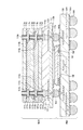
図1は、本発明の第1実施形態に係る半導体装置の構成を示す断面図である。なお、この第1実施形態は、半導体チップ(または半導体ダイ)23がACF接合により実装された半導体パッケージPK11上に、スタックド構造の半導体チップ(または半導体ダイ)33a、33bがワイヤボンド接続された半導体パッケージPK12を積層したものである。
【0028】
図1において、半導体パッケージPK11にはキャリア基板21が設けられ、キャリア基板21の両面にはランド22a、22cがそれぞれ形成されるとともに、キャリア基板21内には内部配線22bが形成されている。そして、キャリア基板21上には、裏面が露出するようにして半導体チップ23がフリップチップ実装され、半導体チップ23には、フリップチップ実装するための突出電極24が設けられている。そして、半導体チップ23に設けられた突出電極24は、異方性導電フィルム25を介してランド22c上にACF(Anisotropic Conductive Film)接合されている。また、キャリア基板21の裏面に設けられたランド22a上には、キャリア基板21をマザー基板上に実装するための突出電極26が設けられている。
【0029】
ここで、ACF接合により半導体チップ23をキャリア基板21上に実装することにより、ワイヤボンドやモールド封止するためのスペースが不要となり、3次元実装時の省スペース化を図ることが可能となるとともに、半導体チップ23をキャリア基板21上に接合する際の低温化を図ることが可能となり、実際の使用時のキャリア基板21の反りを低減することが可能となる。
【0030】
一方、半導体パッケージPK12にはキャリア基板31が設けられ、キャリア基板31の両面にはランド32a、32cがそれぞれ形成されるとともに、キャリア基板31内には内部配線32bが形成されている。そして、キャリア基板31上には、接着層34aを介し半導体チップ33aがフェースアップ実装され、半導体チップ33aは、導電性ワイヤ35aを介してランド32cにワイヤボンド接続されている。さらに、半導体チップ33a上には、導電性ワイヤ35aを避けるようにして、半導体チップ33bがフェースアップ実装され、半導体チップ33bは、接着層34bを介して半導体チップ33a上に固定されるとともに、導電性ワイヤ35bを介してランド32cにワイヤボンド接続されている。
【0031】
また、キャリア基板31の裏面に設けられたランド32a上には、キャリア基板31が半導体チップ23上に離間して保持されるように、キャリア基板31をキャリア基板21上に実装するための突出電極36が設けられている。ここで、突出電極36は、半導体チップ23の搭載領域を避けるようにして配置され、例えば、キャリア基板31の裏面の周囲に突出電極36を配置することができる。そして、キャリア基板21上に設けられたランド22cに突出電極36を接合させることにより、半導体チップ23の裏面が露出された状態で、キャリア基板31がキャリア基板21上に実装されている。
【0032】
これにより、キャリア基板21上にフェースダウン実装された半導体チップ23の裏面が露出された状態で、パッケージングの異なる半導体チップ33a、33bを半導体チップ23上に積層することが可能となる。このため、キャリア基板31をキャリア基板21上に積層した場合においても、半導体チップ23の熱放散性を確保することが可能となるとともに、異種の半導体チップ23、33a、33bの3次元実装構造を実現することが可能となる。
【0033】
また、半導体チップ33a、33bは封止樹脂37により封止され、封止樹脂37は、例えば、エポキシ樹脂などの熱硬化性樹脂を用いたモールド成形などにより形成することができる。
ここで、半導体チップ33a、33bの実装面側のキャリア基板31の一面全体に、モールド成形により封止樹脂37を形成することにより、様々の種類の半導体チップ33a、33bがキャリア基板31上に実装される場合においても、モールド成形時の金型を共通化することが可能となり、封止樹脂工程を効率化することが可能となるとともに、封止樹脂37をセル分割するためのスペースが不要となることから、キャリア基板31上に搭載される半導体チップ33a、33bの搭載面積を増大させることが可能となる。
【0034】
なお、キャリア基板21、31としては、例えば、両面基板、多層配線基板、ビルドアップ基板、テープ基板またはフィルム基板などを用いることができ、キャリア基板21、31の材質としては、例えば、ポリイミド樹脂、ガラスエポキシ樹脂、BTレジン、アラミドとエポキシのコンポジットまたはセラミックなどを用いることができる。また、突出電極24、26、36としては、例えば、Auバンプ、半田材などで被覆されたCuバンプやNiバンプ、あるいは半田ボールなどを用いることができる。ここで、突出電極26、36として、例えば、半田ボールを用いることにより、汎用のBGAを用いることで、異種パッケーPK11、PK12同士を積層することができ、製造ラインを流用することができる。また、導電性ワイヤ35a、35bとしては、例えば、AuワイヤやAlワイヤなどを用いることができる。また、上述した実施形態では、キャリア基板31をキャリア基板21上に実装するために、突出電極36をキャリア基板31のランド32a上に設ける方法について説明したが、突出電極36をキャリア基板21のランド22c上に設けるようにしてもよい。
【0035】
また、上述した実施形態では、ACF接合により半導体チップ23をキャリア基板21上に実装する方法について説明したが、例えば、NCF(Nonconductive Film)接合、ACP(Anisotropic Conductive Paste)接合、NCP(Nonconductive Paste)接合などのその他の圧接接合を用いるようにしてもよく、半田接合や合金接合などの金属接合を用いるようにしてもよい。さらに、上述した実施形態では、キャリア基板21上に半導体チップ23を1個だけ実装する方法を例にとって説明したが、キャリア基板21上に複数の半導体チップを実装するようにしてもよい。
【0036】
図2は、本発明の第2実施形態に係る半導体装置の構成を示す断面図である。なお、この第2実施形態は、半導体チップ43がACF接合により実装された半導体パッケージPK21上に、スタックド構造の半導体チップ53a、53bがそれぞれフリップチップ実装およびワイヤボンド接続された半導体パッケージPK22を積層したものである。
【0037】
図2において、半導体パッケージPK21にはキャリア基板41が設けられ、キャリア基板41の両面にはランド42a、42cがそれぞれ形成されるとともに、キャリア基板41内には内部配線42bが形成されている。そして、キャリア基板41上には、裏面が露出するようにして半導体チップ43がフリップチップ実装され、半導体チップ43には、フリップチップ実装するための突出電極44が設けられている。そして、半導体チップ43に設けられた突出電極44は、異方性導電フィルム45を介してランド42c上にACF接合されている。また、キャリア基板41の裏面に設けられたランド42a上には、キャリア基板41をマザー基板上に実装するための突出電極46が設けられている。
【0038】
ここで、ACF接合により半導体チップ43をキャリア基板41上に実装することにより、ワイヤボンドやモールド封止するためのスペースが不要となり、3次元実装時の省スペース化を図ることが可能となるとともに、半導体チップ43をキャリア基板41上に接合する際の低温化を図ることが可能となり、実際の使用時のキャリア基板41の反りを低減することが可能となる。
【0039】
一方、半導体パッケージPK22にはキャリア基板51が設けられ、キャリア基板51の両面にはランド52a、52cがそれぞれ形成されるとともに、キャリア基板51内には内部配線52bが形成されている。そして、キャリア基板51上には半導体チップ53aがフリップチップ実装され、半導体チップ53aには、フリップチップ実装するための突出電極55aが設けられている。そして、半導体チップ53aに設けられた突出電極55aは、異方性導電フィルム54aを介してランド52c上にACF接合されている。さらに、半導体チップ53a上には、半導体チップ53bがフェースアップ実装され、半導体チップ53bは、接着層54bを介して半導体チップ53a上に固定されるとともに、導電性ワイヤ55bを介してランド52cにワイヤボンド接続されている。
【0040】
ここで、フェースダウン実装された半導体チップ53a上に半導体チップ53bをフェースアップ実装することにより、キャリア基板を介在させることなく、半導体チップ53aよりもサイズが同等かそれ以上の半導体チップ53bを半導体チップ53a上に積層することが可能となり、実装面積を縮小することが可能となる。
【0041】
また、キャリア基板51の裏面に設けられたランド52a上には、キャリア基板51が半導体チップ43上に離間して保持されるようにして、キャリア基板51をキャリア基板51上に実装するための突出電極56が設けられている。ここで、突出電極56は、半導体チップ43の搭載領域を避けるようにして配置され、例えば、キャリア基板51の裏面の周囲に突出電極56を配置することができる。そして、キャリア基板41上に設けられたランド42cに突出電極56を接合させることにより、半導体チップ43の裏面が露出された状態で、キャリア基板51がキャリア基板41上に実装されている。
【0042】
これにより、キャリア基板41上にフェースダウン実装された半導体チップ43の裏面が露出された状態で、パッケージングの異なる半導体チップ53a、53bを半導体チップ43上に積層することが可能となる。このため、キャリア基板51をキャリア基板41上に積層した場合においても、半導体チップ43の熱放散性を確保することが可能となるとともに、異種の半導体チップ43、53a、53bの3次元実装構造を実現することが可能となる。
【0043】
なお、突出電極46、56としては、例えば、半田ボールを用いることができる。これにより、汎用のBGAを用いることで、異種パッケーPK21、PK22同士を積層することができ、製造ラインを流用することができる。
また、半導体チップ53a、53bは封止樹脂57により封止され、封止樹脂57は、例えば、エポキシ樹脂などの熱硬化性樹脂を用いたモールド成形などにより形成することができる。
【0044】
ここで、半導体チップ53a、53bの実装面側のキャリア基板51の一面全体に、モールド成形により封止樹脂57を形成することにより、様々の種類の半導体チップ53a、53bがキャリア基板51上に実装される場合においても、モールド成形時の金型を共通化することが可能となり、封止樹脂工程を効率化することが可能となるとともに、封止樹脂57をセル分割するためのスペースが不要となることから、キャリア基板51上に搭載される半導体チップ53a、53bの搭載面積を増大させることが可能となる。
【0045】
図3は、本発明の第3実施形態に係る半導体装置の製造方法を示す断面図である。なお、この第3実施形態は、複数の半導体チップ62a〜62cを封止樹脂64で一体的にモールド成形した後、個々の半導体チップ62a〜62cごとに切断することにより、半導体チップ62a〜62cがそれぞれ実装されたキャリア基板61a〜61の一面全体に封止樹脂64a〜64cをそれぞれ形成するようにしたものである。
【0046】
図3(a)において、キャリア基板61には、複数の半導体チップ62a〜62cを搭載する搭載領域が設けられている。そして、複数の半導体チップ62a〜62cをキャリア基板61上に実装し、導電性ワイヤ63a〜63cをそれぞれ介してキャリア基板61にワイヤボンド接続する。なお、半導体チップ62a〜62cをワイヤボンド接続する方法以外にも、半導体チップ62a〜62cをキャリア基板61上にフリップチップ実装するようにしてもよく、半導体チップ62a〜62cの積層構造をキャリア基板61上に実装してもよい。
【0047】
次に、図3(b)に示すように、キャリア基板61上に実装された複数の半導体チップ62a〜62cを封止樹脂64で一体的にモールド成形する。ここで、複数の半導体チップ62a〜62cを封止樹脂64で一体的にモールド成形することにより、様々の種類の半導体チップ62a〜62cがキャリア基板61上に実装される場合においても、モールド成形時の金型を共通化することが可能となり、封止樹脂工程を効率化することが可能となるとともに、封止樹脂64をセル分割するためのスペースが不要となることから、キャリア基板61上に搭載される半導体チップ62a〜62cの搭載面積を増大させることが可能となる。
【0048】
次に、図3(c)に示すように、半田ボールなどの突出電極65a〜65cを各キャリア基板61a〜61cの裏面に形成する。そして、図3(d)に示すように、キャリア基板61および封止樹脂64を個々の半導体チップ62a〜62cごとに切断することにより、半導体チップ62a〜62cが封止樹脂64a〜64cでそれぞれ封止されたキャリア基板61a〜61cごとに分割する。また、個々の半導体チップを切断した後に、はんだボールなどの突出電極を形成しても良い。
【0049】
ここで、キャリア基板61および封止樹脂64を一体的に切断することにより、半導体チップ62a〜62cの実装面側のキャリア基板1a〜61cの一面全体に封止樹脂64a〜64cをそれぞれ形成することが可能となる。このため、製造工程の複雑化を抑制しつつ、突出電極65a〜65cの配置領域の剛性を向上させることが可能となり、キャリア基板61a〜61cの反りを低減させることが可能となる。
【0050】
図4は、本発明の第4実施形態に係る半導体装置の製造方法を示す断面図である。なお、この第4実施形態は、半導体チップ73がACF接合により実装された半導体パッケージPK31上に、封止樹脂84で封止された半導体パッケージPK32を積層したものである。
図4(a)において、半導体パッケージPK31にはキャリア基板71が設けられ、キャリア基板71の両面にはランド72a、72bがそれぞれ形成されている。そして、キャリア基板71上には半導体チップ73がフリップチップ実装され、半導体チップ73には、フリップチップ実装するための突出電極74が設けられている。そして、半導体チップ73に設けられた突出電極74は、異方性導電フィルム75を介してランド72b上にACF接合されている。
【0051】
一方、半導体パッケージPK32にはキャリア基板81が設けられ、キャリア基板81の裏面にはランド82が形成され、ランド82上には半田ボールなどの突出電極83が設けられている。また、キャリア基板81上には半導体チップが実装され、半導体チップが実装されたキャリア基板81の一面全体は、封止樹脂84で封止されている。なお、キャリア基板81上には、ワイヤボンド接続された半導体チップを実装するようにしてもよいし、半導体チップをフリップチップ実装するようにしてもよく、半導体チップの積層構造を実装するようにしてもよい。
【0052】
そして、半導体パッケージPK31上に半導体パッケージPK32を積層する場合、キャリア基板71のランド72b上にフラックス76を供給する。なお、キャリア基板71のランド72b上には、フラックス76の代わりに半田ペーストを供給してもよい。
次に、図4(b)に示すように、半導体パッケージPK31上に半導体パッケージPK32をマウントし、リフロー処理を行うことにより、突出電極83をランド72b上に接合させる。
【0053】
次に、図4(c)に示すように、キャリア基板71の裏面に設けられたランド72a上に、キャリア基板71をマザー基板上に実装するための突出電極77を形成する。
図5は、本発明の第5実施形態に係る半導体装置の構成を示す断面図である。なお、この第5実施形態は、半導体チップ103がフリップチップ実装されたキャリア基板101上に、スタックド構造の半導体チップ113a〜113cを3次元実装するようにしたものである。
【0054】
図5において、半導体パッケージPK41にはキャリア基板101が設けられ、キャリア基板101の両面にはランド102a、102cがそれぞれ形成されるとともに、キャリア基板101内には内部配線102bが形成されている。そして、キャリア基板101上には、裏面が露出するようにして半導体チップ103がフリップチップ実装され、半導体チップ103には、フリップチップ実装するための突出電極104が設けられている。そして、半導体チップ103に設けられた突出電極104は、異方性導電フィルム105を介してランド102c上にACF接合されている。なお、半導体チップ103をキャリア基板101上に実装する場合、ACF接合を用いる方法以外にも、例えば、NCF接合や、NCP接合、ACP接合などのその他の圧接接合を用いるようにしてもよく、半田接合や合金接合などの金属接合を用いるようにしてもよい。また、キャリア基板101の裏面に設けられたランド102a上には、キャリア基板101をマザー基板上に実装するための突出電極106が設けられている。
【0055】
一方、半導体パッケージPK42にはキャリア基板111が設けられ、キャリア基板111の両面にはランド112a、112cがそれぞれ形成されるとともに、キャリア基板111内には内部配線112bが形成されている。
また、半導体チップ113a〜113cには、電極パッド114a〜114cがそれぞれ設けられるとともに、各電極パッド114a〜114cが露出するようにして、絶縁膜115a〜115cがそれぞれ設けられている。そして、半導体チップ113a〜113cには、例えば、各電極パッド114a〜114cの位置に対応して、貫通孔116a〜116cがそれぞれ形成され、貫通孔116a〜116c内には、絶縁膜117a〜117cおよび導電膜118a〜118cをそれぞれ介して、貫通電極119a〜119cがそれぞれ形成されている。そして、貫通電極119a〜119cが形成された半導体チップ113a〜113cは、貫通電極119a〜119cをそれぞれ介して積層され、半導体チップ113a〜113c間の隙間には樹脂120a、120bがそれぞれ注入されている。
【0056】
また、半導体チップ113aに形成された貫通電極119a上には、半導体チップ113a〜113cの積層構造をフリップチップ実装するための突出電極121が設けられている。そして、キャリア基板111上に設けられたランド112c上に突出電極121が接合されるとともに、キャリア基板111上に実装された半導体チップ113aの表面が封止樹脂122で封止され、半導体チップ113a〜113cの積層構造がキャリア基板111上に実装されている。
【0057】
また、キャリア基板111の裏面に設けられたランド112a上には、キャリア基板111が半導体チップ103上に離間して保持されるように、キャリア基板111をキャリア基板101上に実装するための突出電極123が設けられている。
ここで、突出電極123は、半導体チップ103の搭載領域を避けるようにして配置され、例えば、キャリア基板111の周囲に突出電極123を配置することができる。そして、キャリア基板101上に設けられたランド102c上に突出電極123を接合させることにより、半導体チップ103の裏面が露出された状態で、キャリア基板111がキャリア基板101上に実装されている。
【0058】
これにより、半導体チップ113a〜113cの積層構造と半導体チップ103との間にキャリア基板を介在させることなく、半導体チップ103の裏面が露出された状態で、半導体チップ103上に半導体チップ111a〜111cの積層構造をフリップチップ実装することが可能となる。このため、積層時の高さの増大を抑制しつつ、半導体チップ103の熱放散性を確保することが可能となり、3次元実装された半導体チップ103、113a〜113cの信頼性の劣化を抑制しつつ、半導体チップ103と異なる種類の半導体チップ113a〜113cを複数積層することが可能となる。
【0059】
なお、突出電極104、106、121、123としては、例えば、Auバンプ、半田材などで被覆されたCuバンプやNiバンプ、あるいは半田ボールなどを用いることができる。また、上述した実施形態では、半導体チップ113a〜113cの3層構造をキャリア基板111上に実装する方法について説明したが、キャリア基板111上に実装される半導体チップの積層構造は、2層または4層以上であってもよい。
【0060】
図6は、本発明の第6実施形態に係る半導体装置の構成を示す断面図である。なお、この第8実施形態は、半導体チップ203がフリップチップ実装されたキャリア基板201上に、W−CSP(ウエハレベル−チップサイズパッケージ)を3次元実装するようにしたものである。
図6において、半導体パッケージPK51にはキャリア基板201が設けられ、キャリア基板201の両面にはランド202a、202cがそれぞれ形成されるとともに、キャリア基板201内には内部配線202bが形成されている。そして、キャリア基板201上には、裏面が露出するようにして半導体チップ203がフリップチップ実装され、半導体チップ203には、フリップチップ実装するための突出電極204が設けられている。そして、半導体チップ203に設けられた突出電極204は、異方性導電フィルム205を介してランド202c上にACF接合されている。また、キャリア基板201の裏面に設けられたランド202a上には、キャリア基板201をマザー基板上に実装するための突出電極206が設けられている。
【0061】
一方、半導体パッケージPK52には半導体チップ211が設けられ、半導体チップ211には、電極パッド212が設けられるとともに、電極パッド212が露出するようにして、絶縁膜213が設けられている。そして、半導体チップ211上には、電極パッド212が露出するようにして応力緩和層214が形成され、電極パッド212上には、応力緩和層214上に延伸された再配置配線215が形成されている。そして、再配置配線215上にはソルダレジスト膜216が形成され、ソルダレジスト膜216には、応力緩和層214上において再配置配線215を露出させる開口部217が形成されている。そして、開口部217を介して露出された再配置配線215上には、半導体パッケージPK52が半導体チップ203上に離間して保持されるように、半導体チップ211をキャリア基板201上にフェースダウン実装するための突出電極218が設けられている。
【0062】
ここで、突出電極218は、半導体チップ203の搭載領域を避けるようにして配置され、例えば、半導体チップ211の周囲に突出電極218を配置することができる。そして、キャリア基板201上に設けられたランド202c上に突出電極218が接合され、半導体チップ203の裏面が露出された状態で、半導体パッケージPK52がキャリア基板201上に実装されている。
【0063】
これにより、半導体チップ203がフリップチップ実装されたキャリア基板201上にW−CSPを積層することができる。このため、半導体チップ203、211の種類またはサイズが異なる場合においても、半導体チップ203、211間にキャリア基板を介在させることなく、半導体チップ203の裏面が露出された状態で、半導体チップ203上に半導体チップ211を3次元実装することが可能となる。この結果、半導体チップ203、211積層時の高さの増大を抑制しつつ、半導体チップ203の熱放散性を確保することが可能となり、3次元実装された半導体チップ203、211の信頼性の劣化を抑制しつつ、半導体チップ203、211実装時の省スペース化を図ることが可能となる。
【0064】
なお、半導体パッケージPK52をキャリア基板201上に実装する場合、例えば、ACF接合やNCF接合などの圧接接合を用いるようにしてもよく、半田接合や合金接合などの金属接合を用いるようにしてもよい。また、突出電極204、206、218としては、例えば、Auバンプ、半田材などで被覆されたCuバンプやNiバンプ、あるいは半田ボールなどを用いることができる。また、上述した実施形態では、キャリア基板201上にフリップチップ実装された1個の半導体チップ203上に半導体パッケージPK52を実装する方法を例にとって説明したが、キャリア基板201上にフリップチップ実装された複数の半導体チップ上に半導体パッケージPK52を実装するようにしてもよい。
【0065】
なお、上述した半導体装置および電子デバイスは、例えば、液晶表示装置、携帯電話、携帯情報端末、ビデオカメラ、デジタルカメラ、MD(Mini Disc)プレーヤなどの電子機器に適用することができ、電子機器の小型・軽量化を可能としつつ、電子機器の信頼性を向上させることができる。
また、上述した実施形態では、半導体チップまたは半導体パッケージを実装する方法を例にとって説明したが、本発明は、必ずしも半導体チップまたは半導体パッケージを実装する方法に限定されることなく、例えば、弾性表面波(SAW)素子などのセラミック素子、光変調器や光スイッチなどの光学素子、磁気センサやバイオセンサなどの各種センサ類などを実装するようにしてもよい。
【図面の簡単な説明】
【図1】第1実施形態に係る半導体装置の構成を示す断面図。
【図2】第2実施形態に係る半導体装置の構成を示す断面図。
【図3】第3実施形態に係る半導体装置の構成を示す断面図。
【図4】第4実施形態に係る半導体装置の製造方法を示す断面図。
【図5】第5実施形態に係る半導体装置の製造方法を示す断面図。
【図6】第6実施形態に係る半導体装置の構成を示す断面図。
【符号の説明】
21、31、41、51、61、61a〜61c、71、81、101、111、201 キャリア基板、22a、22c、32a、32c、42a、42c、52a、52c、72a、72b、82、102a、102c、112a、112c、202a、202c ランド、、22b、32b、42b、52b、102b、112b、202b 内部配線、23、33a、33b、43、53a、53b、62a〜62c、73、103、113a〜113c、203、211 半導体チップ、、24、26、36、44、46、55a、56、65a〜65c、74、77、83、104、121、123、206、218 突出電極、25、45、54a、75、105、205 異方性導電フィルム、34a、34b、54b 接着層、15、35a、35b、55b、63a〜63c 導電性ワイヤ、37、57、64、64a〜64c、84、120a、120b、122 封止樹脂、76 フラックス、114a〜114c、212 電極パッド、115a〜115c、117a〜117c、213 絶縁膜、116a〜116c 貫通孔、118a〜118c 導電膜、119a〜119c 貫通電極、214 応力緩和層、215 再配置配線、216 ソルダレジスト層、217 開口部、PK11、PK12、PK21、PK22、PK31、PK32、PK41、PK42、PK51、PK52 半導体パッケージ[0001]
TECHNICAL FIELD OF THE INVENTION
The present invention relates to a semiconductor device, an electronic device, an electronic apparatus, a method for manufacturing a semiconductor device, and a method for manufacturing an electronic device, and is particularly suitable for being applied to a laminated structure such as a semiconductor package.
[0002]
[Prior art]
In a conventional semiconductor device, there is a method of three-dimensionally mounting a semiconductor chip via a carrier substrate, for example, as disclosed in Patent Document 1, in order to save space when mounting the semiconductor chip.
[0003]
[Patent Document 1]
JP-A-10-284683
[0004]
[Problems to be solved by the invention]
However, the method of three-dimensionally mounting a semiconductor chip via a carrier substrate has a problem that it is difficult to stack different kinds of chips while ensuring heat dissipation.
Therefore, an object of the present invention is to provide a semiconductor device, an electronic device, an electronic apparatus, a method of manufacturing a semiconductor device, and a method of manufacturing an electronic device, which can realize a three-dimensional mounting structure of different types of chips while securing heat dissipation. It is to provide.
[0005]
[Means for Solving the Problems]
According to one embodiment of the present invention, there is provided a semiconductor device including a first carrier substrate, a first semiconductor chip face-down mounted on the first carrier substrate, and a second carrier substrate. And a second semiconductor chip mounted on the second carrier substrate, and the second carrier substrate and the first carrier substrate so that the second carrier substrate is held on the first semiconductor chip. A protruding electrode to be connected, a sealing material for sealing the second semiconductor chip, and a sealing material provided between the first carrier substrate and the second carrier substrate so that a back surface of the first semiconductor chip is exposed. Characterized in that the resin is provided.
[0006]
This makes it possible to stack the second semiconductor chips having different packaging on the first semiconductor chip in a state where the back surface of the first semiconductor chip face-down mounted on the first carrier substrate is exposed. For this reason, even when the second carrier substrate is laminated on the first carrier substrate, it is possible to ensure the heat dissipation of the first semiconductor chip and to realize a three-dimensional mounting structure of different types of chips. It becomes possible.
[0007]
Further, according to the semiconductor device of one embodiment of the present invention, the second carrier substrate is fixed on the first carrier substrate so as to extend over the first semiconductor chip.
As a result, the first semiconductor chip and the second semiconductor chip can be arranged one on top of the other, and the mounting area when mounting a plurality of semiconductor chips is reduced, thereby saving space when mounting the semiconductor chips. Becomes possible.
[0008]
Further, according to the semiconductor device of one embodiment of the present invention, the sealing material is a mold resin.
This makes it possible to stack different types of packages including the second carrier substrate on the first carrier substrate, and realize a three-dimensional mounting structure of the semiconductor chip even when the types of the semiconductor chips are different. .
[0009]
Further, according to the semiconductor device of one embodiment of the present invention, the side wall of the sealing material coincides with the position of the side wall of the second carrier substrate.
Thereby, the entire surface of the second carrier substrate is reinforced with the sealing material for sealing the second semiconductor chip while suppressing an increase in height when the second carrier substrate is stacked on the first carrier substrate. It is possible to seal the second semiconductor chip without dividing the sealing material into cells, and to increase the mounting area of the second semiconductor chip mounted on the second carrier substrate. Becomes possible.
[0010]
Further, according to the semiconductor device of one embodiment of the present invention, the first semiconductor chip is connected to the first carrier substrate by pressure contact bonding.
This makes it possible to lower the temperature when connecting the first semiconductor chip on the first carrier substrate, and to reduce the warpage of the first carrier substrate during actual use.
[0011]
Further, according to the semiconductor device of one embodiment of the present invention, the semiconductor device including the first carrier substrate and the first semiconductor chip mounted on the first carrier substrate, the second carrier substrate and the second carrier The semiconductor device is characterized by having a different elastic modulus at the same temperature from the semiconductor device including the second semiconductor chip mounted on the substrate.
This makes it possible to suppress the warpage generated on one carrier substrate by the other carrier substrate, and to improve the connection reliability between the first carrier substrate and the second carrier substrate.
[0012]
Further, according to the semiconductor device of one aspect of the present invention, the first carrier substrate on which the first semiconductor chip is mounted is a ball grid array on which flip chip mounting is performed, and the second carrier on which the second semiconductor chip is mounted. The substrate is a mold-sealed ball grid array or chip size package.
This makes it possible to stack different types of packages while suppressing an increase in the height of the three-dimensional mounting structure, and to save space when mounting a semiconductor chip even when the types of semiconductor chips are different. It becomes.
[0013]
Further, according to the semiconductor device of one embodiment of the present invention, the first semiconductor chip is a plurality of semiconductor chips mounted in parallel on the first carrier substrate.
As a result, the second semiconductor chip can be stacked on the plurality of first semiconductor chips, and the mounting area for mounting the plurality of semiconductor chips can be reduced, thereby saving space when mounting the semiconductor chips. It becomes possible to plan.
[0014]
Further, according to the semiconductor device of one embodiment of the present invention, the second semiconductor chip is a plurality of stacked semiconductor chips.
As a result, a plurality of second semiconductor chips of different types or sizes can be stacked on the first semiconductor chip, and various functions can be provided while saving space when mounting the semiconductor chip. Becomes possible.
[0015]
Further, according to the semiconductor device of one embodiment of the present invention, the second semiconductor chip is a plurality of semiconductor chips mounted in parallel on the second carrier substrate.
Accordingly, it is possible to stack a plurality of second semiconductor chips on the first semiconductor chip while suppressing an increase in height when the second semiconductor chips are stacked, thereby deteriorating connection reliability during three-dimensional mounting. It is possible to save space when mounting a semiconductor chip while suppressing the above.
[0016]
Further, according to the semiconductor device of one embodiment of the present invention, the carrier substrate, the first semiconductor chip face-down mounted on the carrier substrate, and the rearrangement wiring layer formed on the formation surface of the electrode pad A second semiconductor chip; and a protruding electrode for connecting the second semiconductor chip to the carrier substrate such that the second semiconductor chip is held on the first semiconductor chip.
[0017]
Thus, even when the types or sizes of the semiconductor chips are different, the first semiconductor chip is exposed in a state in which the back surface of the first semiconductor chip is exposed without interposing a carrier substrate between the first semiconductor chip and the second semiconductor chip. With the second semiconductor chip arranged on one semiconductor chip, the second semiconductor chip can be flip-chip mounted on the carrier substrate.
[0018]
For this reason, it is possible to secure heat dissipation while suppressing an increase in height when semiconductor chips are stacked, and to suppress a deterioration in the reliability of the three-dimensionally mounted semiconductor chip, Space can be saved.
Further, according to the electronic device of one embodiment of the present invention, the first carrier substrate, the first electronic component mounted on the first carrier substrate, the second carrier substrate, and the second carrier substrate A second electronic component mounted thereon, a protruding electrode connecting the second carrier substrate and the first carrier substrate so that the second carrier substrate is held on the first electronic component, A sealing material for sealing the electronic component; and a resin provided between the first carrier substrate and the second carrier substrate so that a back surface of the first electronic component is exposed. And
[0019]
This makes it possible to stack second electronic components having different packaging on the first electronic component in a state where the back surface of the first electronic component mounted face-down on the first carrier substrate is exposed. For this reason, even when the second carrier substrate is laminated on the first carrier substrate, it is possible to ensure the heat dissipation of the first electronic component and to realize a three-dimensional mounting structure of different types of components. It becomes possible.
[0020]
According to the electronic device of one embodiment of the present invention, the first carrier substrate, the first semiconductor chip mounted on the first carrier substrate, the second carrier substrate, and the second carrier substrate A second semiconductor chip mounted thereon, a protruding electrode connecting the second carrier substrate and the first carrier substrate so that the second carrier substrate is held on the first semiconductor chip, A sealing material for sealing a semiconductor chip; a resin provided between the first carrier substrate and the second carrier substrate so that a back surface of the first semiconductor chip is exposed; A mother board on which the board is mounted.
[0021]
Thereby, it is possible to stack the second semiconductor chips having different packaging on the first semiconductor chip in a state where the back surface of the first semiconductor chip face-down mounted on the first carrier substrate is exposed. It is possible to realize a three-dimensional mounting structure of different types of chips while ensuring the heat dissipation of one semiconductor chip.
According to the method for manufacturing a semiconductor device of one embodiment of the present invention, the step of mounting the first semiconductor chip face-down on the first carrier substrate so that the back surface is exposed; A step of mounting a second semiconductor chip, a step of sealing the second semiconductor chip with a sealing resin, and the step of projecting the second carrier substrate so that the second carrier substrate is separated and held on the first semiconductor chip. Connecting the second carrier substrate and the first carrier substrate via an electrode.
[0022]
Thus, even when the second carrier substrate is stacked on the first carrier substrate, the back surface of the first semiconductor chip face-down mounted on the first carrier substrate can be exposed. For this reason, it is possible to efficiently dissipate the heat generated from the first semiconductor chip, and to stack the second semiconductor chips having different packaging on the first semiconductor chip, thereby ensuring heat dissipation. Thus, a three-dimensional mounting structure of different types of chips can be realized.
[0023]
According to the method for manufacturing a semiconductor device of one embodiment of the present invention, the step of sealing the second semiconductor chip with the sealing resin includes the step of sealing the plurality of second semiconductor chips mounted on the second carrier substrate. And a step of cutting the second carrier substrate molded with the sealing resin for each of the second semiconductor chips.
[0024]
This makes it possible to seal the second semiconductor chip with the sealing resin without dividing the sealing resin into cells for each of the second semiconductor chips, and to seal the entire surface of the second carrier substrate. It becomes possible to reinforce with resin.
For this reason, even when the type or size of the second semiconductor chip is different, it is possible to use a common mold at the time of molding, to make the sealing resin process more efficient, and to divide the cell. Since no space is required for the second semiconductor chip, the mounting area of the second semiconductor chip mounted on the second carrier substrate can be increased.
[0025]
According to the method for manufacturing an electronic device of one embodiment of the present invention, the step of mounting the first electronic component on the first carrier substrate so that the back surface is exposed; A step of mounting a component, a step of sealing the second electronic component with a sealing resin, and a step of interposing the protruding electrode so that the second carrier substrate is separated and held on the first electronic component. Connecting the second carrier substrate and the first carrier substrate.
[0026]
Thus, even when the second carrier substrate is stacked on the first carrier substrate, the back surface of the first electronic component mounted face-down on the first carrier substrate can be exposed. For this reason, it is possible to efficiently dissipate the heat generated from the first electronic component, and to stack the second electronic component having different packaging on the first electronic component, thereby ensuring heat dissipation. In addition, it is possible to realize a three-dimensional mounting structure of different components.
[0027]
BEST MODE FOR CARRYING OUT THE INVENTION
Hereinafter, a semiconductor device, an electronic device, and a manufacturing method thereof according to an embodiment of the present invention will be described with reference to the drawings.
FIG. 1 is a sectional view showing a configuration of the semiconductor device according to the first embodiment of the present invention. In the first embodiment, a semiconductor chip (or semiconductor die) 33a, 33b having a stacked structure is wire-bonded on a semiconductor package PK11 on which a semiconductor chip (or semiconductor die) 23 is mounted by ACF bonding. The package PK12 is stacked.
[0028]
In FIG. 1, a
[0029]
Here, by mounting the
[0030]
On the other hand, a
[0031]
In addition, projecting electrodes for mounting the
[0032]
Thus, the
[0033]
The
Here, various types of
[0034]
In addition, as the
[0035]
Further, in the above-described embodiment, the method of mounting the
[0036]
FIG. 2 is a cross-sectional view illustrating a configuration of a semiconductor device according to a second embodiment of the present invention. In the second embodiment, a semiconductor package PK22 in which
[0037]
In FIG. 2, a carrier substrate 41 is provided on a semiconductor package PK21, lands 42a and 42c are formed on both surfaces of the carrier substrate 41, and an
[0038]
Here, by mounting the
[0039]
On the other hand, a
[0040]
Here, by mounting the
[0041]
Also, on the
[0042]
Thus, the
[0043]
In addition, as the protruding
The
[0044]
Here, various types of
[0045]
FIG. 3 is a sectional view illustrating the method for manufacturing the semiconductor device according to the third embodiment of the present invention. In the third embodiment, after the plurality of
[0046]
In FIG. 3A, a mounting area for mounting a plurality of
[0047]
Next, as shown in FIG. 3B, the plurality of
[0048]
Next, as shown in FIG. 3C, protruding
[0049]
Here, by integrally cutting the
[0050]
FIG. 4 is a sectional view illustrating a method for manufacturing a semiconductor device according to a fourth embodiment of the present invention. In the fourth embodiment, a semiconductor package PK32 sealed with a sealing
In FIG. 4A, a
[0051]
On the other hand, a
[0052]
Then, when stacking the semiconductor package PK32 on the semiconductor package PK31, the
Next, as shown in FIG. 4B, the semiconductor package PK32 is mounted on the semiconductor package PK31, and the protruding
[0053]
Next, as shown in FIG. 4C, projecting
FIG. 5 is a cross-sectional view illustrating a configuration of a semiconductor device according to a fifth embodiment of the present invention. In the fifth embodiment,
[0054]
In FIG. 5, a
[0055]
On the other hand, a
The
[0056]
Further, on the through
[0057]
Further, projecting electrodes for mounting the
Here, the projecting
[0058]
This allows the semiconductor chips 111a to 111c to be mounted on the
[0059]
As the protruding
[0060]
FIG. 6 is a cross-sectional view illustrating a configuration of a semiconductor device according to a sixth embodiment of the present invention. In the eighth embodiment, a W-CSP (wafer level-chip size package) is three-dimensionally mounted on a
6, a
[0061]
On the other hand, a
[0062]
Here, the protruding
[0063]
Thereby, the W-CSP can be stacked on the
[0064]
In the case where the semiconductor package PK52 is mounted on the
[0065]
Note that the above-described semiconductor device and electronic device can be applied to electronic devices such as a liquid crystal display device, a mobile phone, a personal digital assistant, a video camera, a digital camera, and an MD (Mini Disc) player. The reliability of the electronic device can be improved while enabling reduction in size and weight.
Further, in the above-described embodiment, a method of mounting a semiconductor chip or a semiconductor package has been described as an example. However, the present invention is not necessarily limited to a method of mounting a semiconductor chip or a semiconductor package. A ceramic element such as a (SAW) element, an optical element such as an optical modulator or an optical switch, or various sensors such as a magnetic sensor or a biosensor may be mounted.
[Brief description of the drawings]
FIG. 1 is a sectional view showing a configuration of a semiconductor device according to a first embodiment.
FIG. 2 is a sectional view showing a configuration of a semiconductor device according to a second embodiment.
FIG. 3 is a sectional view showing a configuration of a semiconductor device according to a third embodiment.
FIG. 4 is a sectional view showing a method for manufacturing a semiconductor device according to a fourth embodiment.
FIG. 5 is a sectional view showing a method for manufacturing a semiconductor device according to a fifth embodiment.
FIG. 6 is a sectional view showing a configuration of a semiconductor device according to a sixth embodiment.
[Explanation of symbols]
21, 31, 41, 51, 61, 61a to 61c, 71, 81, 101, 111, 201 Carrier substrate, 22a, 22c, 32a, 32c, 42a, 42c, 52a, 52c, 72a, 72b, 82, 102a, 102c, 112a, 112c, 202a, 202c Land, 22b, 32b, 42b, 52b, 102b, 112b, 202b Internal wiring, 23, 33a, 33b, 43, 53a, 53b, 62a to 62c, 73, 103, 113a to 113a 113c, 203, 211 Semiconductor chip, 24, 26, 36, 44, 46, 55a, 56, 65a to 65c, 74, 77, 83, 104, 121, 123, 206, 218 Projecting electrode, 25, 45, 54a , 75, 105, 205 anisotropic conductive film, 34a, 34b, 54b adhesive layer, 15 , 35a, 35b, 55b, 63a to 63c conductive wire, 37, 57, 64, 64a to 64c, 84, 120a, 120b, 122 sealing resin, 76 flux, 114a to 114c, 212 electrode pad, 115a to 115c, 117a-117c, 213 insulating film, 116a-116c through hole, 118a-118c conductive film, 119a-119c through electrode, 214 stress relaxation layer, 215 relocation wiring, 216 solder resist layer, 217 opening, PK11, PK12, PK21 , PK22, PK31, PK32, PK41, PK42, PK51, PK52 Semiconductor packages
Claims (16)
前記第1キャリア基板上にフェースダウン実装された第1半導体チップと、
第2キャリア基板と、
前記第2キャリア基板上に搭載された第2半導体チップと、
前記第2キャリア基板が前記第1半導体チップ上に保持されるように、前記第2キャリア基板と前記第1キャリア基板とを接続する突出電極と、
前記第2半導体チップを封止する封止材と、
前記第1半導体チップの裏面が露出されるように、前記第1キャリア基板と前記第2キャリア基板との間に設けられた樹脂とを備えることを特徴とする半導体装置。A first carrier substrate;
A first semiconductor chip face-down mounted on the first carrier substrate;
A second carrier substrate;
A second semiconductor chip mounted on the second carrier substrate;
A protruding electrode connecting the second carrier substrate and the first carrier substrate so that the second carrier substrate is held on the first semiconductor chip;
A sealing material for sealing the second semiconductor chip;
A semiconductor device, comprising: a resin provided between the first carrier substrate and the second carrier substrate such that a back surface of the first semiconductor chip is exposed.
前記キャリア基板上にフェースダウン実装された第1半導体チップと、
電極パッドの形成面上に再配置配線層が形成された第2半導体チップと、
前記第2半導体チップが前記第1半導体チップ上に保持されるように、前記第2半導体チップと前記キャリア基板とを接続する突出電極とを備えることを特徴とする半導体装置。A carrier substrate,
A first semiconductor chip face-down mounted on the carrier substrate;
A second semiconductor chip having a redistribution wiring layer formed on a surface on which the electrode pads are formed;
A semiconductor device comprising: a protruding electrode that connects the second semiconductor chip and the carrier substrate so that the second semiconductor chip is held on the first semiconductor chip.
前記第1キャリア基板上に搭載された第1電子部品と、
第2キャリア基板と、
前記第2キャリア基板上に搭載された第2電子部品と、
前記第2キャリア基板が前記第1電子部品上に保持されるように、前記第2キャリア基板と前記第1キャリア基板とを接続する突出電極と、
前記第2電子部品を封止する封止材と、
前記第1電子部品の裏面が露出されるように、前記第1キャリア基板と前記第2キャリア基板との間に設けられた樹脂とを備えることを特徴とする電子デバイス。A first carrier substrate;
A first electronic component mounted on the first carrier substrate;
A second carrier substrate;
A second electronic component mounted on the second carrier substrate;
Projecting electrodes connecting the second carrier substrate and the first carrier substrate so that the second carrier substrate is held on the first electronic component;
A sealing material for sealing the second electronic component;
An electronic device, comprising: a resin provided between the first carrier substrate and the second carrier substrate so that a back surface of the first electronic component is exposed.
前記第1キャリア基板上に搭載された第1半導体チップと、
第2キャリア基板と、
前記第2キャリア基板上に搭載された第2半導体チップと、
前記第2キャリア基板が前記第1半導体チップ上に保持されるように、前記第2キャリア基板と前記第1キャリア基板とを接続する突出電極と、
前記第2半導体チップを封止する封止材と、
前記第1半導体チップの裏面が露出されるように、前記第1キャリア基板と前記第2キャリア基板との間に設けられた樹脂と、
前記第1キャリア基板が実装されたマザー基板とを備えることを特徴とする電子機器。A first carrier substrate;
A first semiconductor chip mounted on the first carrier substrate;
A second carrier substrate;
A second semiconductor chip mounted on the second carrier substrate;
A protruding electrode connecting the second carrier substrate and the first carrier substrate so that the second carrier substrate is held on the first semiconductor chip;
A sealing material for sealing the second semiconductor chip;
A resin provided between the first carrier substrate and the second carrier substrate so that a back surface of the first semiconductor chip is exposed;
An electronic device, comprising: a mother board on which the first carrier board is mounted.
第2キャリア基板上に第2半導体チップを実装する工程と、
前記第2半導体チップを封止樹脂で封止する工程と、
前記第2キャリア基板が前記第1半導体チップ上に離間して保持されるように、前記突出電極を介して前記第2キャリア基板と前記第1キャリア基板とを接続する工程とを備えることを特徴とする半導体装置の製造方法。Mounting the first semiconductor chip face down on the first carrier substrate such that the back surface is exposed;
Mounting a second semiconductor chip on a second carrier substrate;
Sealing the second semiconductor chip with a sealing resin;
Connecting the second carrier substrate and the first carrier substrate via the protruding electrodes such that the second carrier substrate is held apart on the first semiconductor chip. Manufacturing method of a semiconductor device.
前記第2キャリア基板に実装された複数の第2半導体チップを封止樹脂で一体的にモールド成形する工程と、
前記封止樹脂によりモールド成形された前記第2キャリア基板を前記第2半導体チップごとに切断する工程とを備えることを特徴とする請求項14記載の半導体装置の製造方法。The step of sealing the second semiconductor chip with the sealing resin includes:
A step of integrally molding a plurality of second semiconductor chips mounted on the second carrier substrate with a sealing resin;
The method of manufacturing a semiconductor device according to claim 14, further comprising: cutting the second carrier substrate molded with the sealing resin for each of the second semiconductor chips.
第2キャリア基板上に第2電子部品を実装する工程と、
前記第2電子部品を封止樹脂で封止する工程と、
前記第2キャリア基板が前記第1電子部品上に離間して保持されるように、前記突出電極を介して前記第2キャリア基板と前記第1キャリア基板とを接続する工程とを備えることを特徴とする電子デバイスの製造方法。Mounting the first electronic component on the first carrier substrate such that the back surface is exposed;
Mounting a second electronic component on a second carrier substrate;
Sealing the second electronic component with a sealing resin;
Connecting the second carrier substrate and the first carrier substrate via the protruding electrodes so that the second carrier substrate is held apart on the first electronic component. Method for manufacturing an electronic device.
Priority Applications (3)
| Application Number | Priority Date | Filing Date | Title |
|---|---|---|---|
| JP2003074219A JP2004281920A (en) | 2003-03-18 | 2003-03-18 | Semiconductor device, electronic device, electronic apparatus, process for producing semiconductor device, and process for producing electronic device |
| CNB2004100287544A CN100442502C (en) | 2003-03-18 | 2004-03-15 | Semiconductor, electronic device and their producing method and electronic instrument |
| US10/801,927 US20050110166A1 (en) | 2003-03-18 | 2004-03-16 | Semiconductor device, electronic device, electronic apparatus, method of manufacturing semiconductor device, and method of manufacturing electronic device |
Applications Claiming Priority (1)
| Application Number | Priority Date | Filing Date | Title |
|---|---|---|---|
| JP2003074219A JP2004281920A (en) | 2003-03-18 | 2003-03-18 | Semiconductor device, electronic device, electronic apparatus, process for producing semiconductor device, and process for producing electronic device |
Publications (1)
| Publication Number | Publication Date |
|---|---|
| JP2004281920A true JP2004281920A (en) | 2004-10-07 |
Family
ID=33289923
Family Applications (1)
| Application Number | Title | Priority Date | Filing Date |
|---|---|---|---|
| JP2003074219A Withdrawn JP2004281920A (en) | 2003-03-18 | 2003-03-18 | Semiconductor device, electronic device, electronic apparatus, process for producing semiconductor device, and process for producing electronic device |
Country Status (3)
| Country | Link |
|---|---|
| US (1) | US20050110166A1 (en) |
| JP (1) | JP2004281920A (en) |
| CN (1) | CN100442502C (en) |
Cited By (4)
| Publication number | Priority date | Publication date | Assignee | Title |
|---|---|---|---|---|
| JP2008016519A (en) * | 2006-07-04 | 2008-01-24 | Renesas Technology Corp | Semiconductor device and its manufacturing method |
| CN102130078B (en) * | 2010-01-20 | 2013-03-13 | 财团法人工业技术研究院 | Heat-conducting insulated composite film and chip stacking structures |
| US20170301598A1 (en) * | 2005-08-19 | 2017-10-19 | Micron Technology, Inc. | Microelectronic devices, stacked microelectronic devices, and methods for manufacturing microelectronic devices |
| US10756075B2 (en) | 2018-05-24 | 2020-08-25 | Samsung Electronics Co., Ltd. | Package-on-package type semiconductor package and method for manufacturing the same |
Families Citing this family (10)
| Publication number | Priority date | Publication date | Assignee | Title |
|---|---|---|---|---|
| TWI283467B (en) * | 2003-12-31 | 2007-07-01 | Advanced Semiconductor Eng | Multi-chip package structure |
| US20070013042A1 (en) * | 2005-06-20 | 2007-01-18 | Nokia Corporation | Electronic module assembly with heat spreader |
| JP4512545B2 (en) | 2005-10-27 | 2010-07-28 | パナソニック株式会社 | Multilayer semiconductor module |
| KR101808478B1 (en) * | 2011-08-16 | 2017-12-12 | 인텔 코포레이션 | Package-on-package structure |
| CN102693968B (en) | 2012-05-25 | 2014-12-03 | 华为技术有限公司 | Chip stacking and packaging structure |
| CN103972202A (en) * | 2013-01-31 | 2014-08-06 | 联想(北京)有限公司 | Circuit device and PCB (printed circuit board) |
| KR102103375B1 (en) | 2013-06-18 | 2020-04-22 | 삼성전자주식회사 | A semiconductor package |
| US20170016745A1 (en) * | 2014-03-24 | 2017-01-19 | Panasonic Intellectual Property Management Co., Ltd. | Magnetic sensor |
| WO2016056179A1 (en) * | 2014-10-09 | 2016-04-14 | パナソニックIpマネジメント株式会社 | Magnetic sensor |
| US12046523B2 (en) * | 2019-11-12 | 2024-07-23 | Advanced Semiconductor Engineering, Inc. | Semiconductor device packages and methods of manufacturing the same |
Family Cites Families (43)
| Publication number | Priority date | Publication date | Assignee | Title |
|---|---|---|---|---|
| JPH03273673A (en) * | 1990-03-23 | 1991-12-04 | Matsushita Electron Corp | Semiconductor device |
| US5120678A (en) * | 1990-11-05 | 1992-06-09 | Motorola Inc. | Electrical component package comprising polymer-reinforced solder bump interconnection |
| US5222014A (en) * | 1992-03-02 | 1993-06-22 | Motorola, Inc. | Three-dimensional multi-chip pad array carrier |
| GB9312328D0 (en) * | 1993-06-15 | 1993-07-28 | Lexor Technology Limited | A method of brazing |
| KR0134648B1 (en) * | 1994-06-09 | 1998-04-20 | 김광호 | Multi-chip package |
| JPH08115989A (en) * | 1994-08-24 | 1996-05-07 | Fujitsu Ltd | Semiconductor device and its manufacture |
| KR19990067623A (en) * | 1995-11-28 | 1999-08-25 | 가나이 쓰도무 | Semiconductor device, manufacturing method and mounting board |
| JPH10163386A (en) * | 1996-12-03 | 1998-06-19 | Toshiba Corp | Semiconductor device, semiconductor package and mounting circuit device |
| US5994166A (en) * | 1997-03-10 | 1999-11-30 | Micron Technology, Inc. | Method of constructing stacked packages |
| JP2964983B2 (en) * | 1997-04-02 | 1999-10-18 | 日本電気株式会社 | Three-dimensional memory module and semiconductor device using the same |
| JPH10294423A (en) * | 1997-04-17 | 1998-11-04 | Nec Corp | Semiconductor device |
| US6180881B1 (en) * | 1998-05-05 | 2001-01-30 | Harlan Ruben Isaak | Chip stack and method of making same |
| US6369444B1 (en) * | 1998-05-19 | 2002-04-09 | Agere Systems Guardian Corp. | Packaging silicon on silicon multichip modules |
| JP3201353B2 (en) * | 1998-08-04 | 2001-08-20 | 日本電気株式会社 | Semiconductor device and manufacturing method thereof |
| US6133634A (en) * | 1998-08-05 | 2000-10-17 | Fairchild Semiconductor Corporation | High performance flip chip package |
| SG75873A1 (en) * | 1998-09-01 | 2000-10-24 | Texas Instr Singapore Pte Ltd | Stacked flip-chip integrated circuit assemblage |
| TW434767B (en) * | 1998-09-05 | 2001-05-16 | Via Tech Inc | Package architecture of ball grid array integrated circuit device |
| US6573119B1 (en) * | 1999-02-17 | 2003-06-03 | Hitachi, Ltd. | Semiconductor device and method of manufacture thereof |
| US6023097A (en) * | 1999-03-17 | 2000-02-08 | Chipmos Technologies, Inc. | Stacked multiple-chip module micro ball grid array packaging |
| US6034425A (en) * | 1999-03-17 | 2000-03-07 | Chipmos Technologies Inc. | Flat multiple-chip module micro ball grid array packaging |
| JP2000349255A (en) * | 1999-06-03 | 2000-12-15 | Oki Electric Ind Co Ltd | Semiconductor storage device and manufacture thereof |
| US6122171A (en) * | 1999-07-30 | 2000-09-19 | Micron Technology, Inc. | Heat sink chip package and method of making |
| TW415056B (en) * | 1999-08-05 | 2000-12-11 | Siliconware Precision Industries Co Ltd | Multi-chip packaging structure |
| JP2001156212A (en) * | 1999-09-16 | 2001-06-08 | Nec Corp | Resin sealed semiconductor device and producing method therefor |
| JP3798597B2 (en) * | 1999-11-30 | 2006-07-19 | 富士通株式会社 | Semiconductor device |
| JP3881488B2 (en) * | 1999-12-13 | 2007-02-14 | 株式会社東芝 | Circuit module cooling device and electronic apparatus having the cooling device |
| US6369448B1 (en) * | 2000-01-21 | 2002-04-09 | Lsi Logic Corporation | Vertically integrated flip chip semiconductor package |
| US6731009B1 (en) * | 2000-03-20 | 2004-05-04 | Cypress Semiconductor Corporation | Multi-die assembly |
| JP2001339011A (en) * | 2000-03-24 | 2001-12-07 | Shinko Electric Ind Co Ltd | Semiconductor device and its manufacturing method |
| JP2001352035A (en) * | 2000-06-07 | 2001-12-21 | Sony Corp | Assembling jig for multilayer semiconductor device and manufacturing method therefor |
| US6461881B1 (en) * | 2000-06-08 | 2002-10-08 | Micron Technology, Inc. | Stereolithographic method and apparatus for fabricating spacers for semiconductor devices and resulting structures |
| JP2002134650A (en) * | 2000-10-23 | 2002-05-10 | Rohm Co Ltd | Semiconductor device and its manufacturing method |
| US6734539B2 (en) * | 2000-12-27 | 2004-05-11 | Lucent Technologies Inc. | Stacked module package |
| US6395622B1 (en) * | 2001-06-05 | 2002-05-28 | Chipmos Technologies Inc. | Manufacturing process of semiconductor devices |
| US6686225B2 (en) * | 2001-07-27 | 2004-02-03 | Texas Instruments Incorporated | Method of separating semiconductor dies from a wafer |
| US6787916B2 (en) * | 2001-09-13 | 2004-09-07 | Tru-Si Technologies, Inc. | Structures having a substrate with a cavity and having an integrated circuit bonded to a contact pad located in the cavity |
| JP3866591B2 (en) * | 2001-10-29 | 2007-01-10 | 富士通株式会社 | Method for forming interelectrode connection structure and interelectrode connection structure |
| JP2003218150A (en) * | 2002-01-23 | 2003-07-31 | Fujitsu Media Device Kk | Module parts |
| JP2003318361A (en) * | 2002-04-19 | 2003-11-07 | Fujitsu Ltd | Semiconductor device and method of manufacturing the same |
| US6903458B1 (en) * | 2002-06-20 | 2005-06-07 | Richard J. Nathan | Embedded carrier for an integrated circuit chip |
| JP4072020B2 (en) * | 2002-08-09 | 2008-04-02 | 日本電波工業株式会社 | Surface mount crystal oscillator |
| JP2004179232A (en) * | 2002-11-25 | 2004-06-24 | Seiko Epson Corp | Semiconductor device, manufacturing method thereof, and electronic apparatus |
| JP4096774B2 (en) * | 2003-03-24 | 2008-06-04 | セイコーエプソン株式会社 | SEMICONDUCTOR DEVICE, ELECTRONIC DEVICE, ELECTRONIC DEVICE, SEMICONDUCTOR DEVICE MANUFACTURING METHOD, AND ELECTRONIC DEVICE MANUFACTURING METHOD |
-
2003
- 2003-03-18 JP JP2003074219A patent/JP2004281920A/en not_active Withdrawn
-
2004
- 2004-03-15 CN CNB2004100287544A patent/CN100442502C/en not_active Expired - Fee Related
- 2004-03-16 US US10/801,927 patent/US20050110166A1/en not_active Abandoned
Cited By (6)
| Publication number | Priority date | Publication date | Assignee | Title |
|---|---|---|---|---|
| US20170301598A1 (en) * | 2005-08-19 | 2017-10-19 | Micron Technology, Inc. | Microelectronic devices, stacked microelectronic devices, and methods for manufacturing microelectronic devices |
| US10431513B2 (en) * | 2005-08-19 | 2019-10-01 | Micron Technology, Inc. | Microelectronic devices, stacked microelectronic devices, and methods for manufacturing microelectronic devices |
| US11239128B2 (en) | 2005-08-19 | 2022-02-01 | Micron Technology, Inc. | Microelectronic devices, stacked microelectronic devices, and methods for manufacturing microelectronic devices |
| JP2008016519A (en) * | 2006-07-04 | 2008-01-24 | Renesas Technology Corp | Semiconductor device and its manufacturing method |
| CN102130078B (en) * | 2010-01-20 | 2013-03-13 | 财团法人工业技术研究院 | Heat-conducting insulated composite film and chip stacking structures |
| US10756075B2 (en) | 2018-05-24 | 2020-08-25 | Samsung Electronics Co., Ltd. | Package-on-package type semiconductor package and method for manufacturing the same |
Also Published As
| Publication number | Publication date |
|---|---|
| US20050110166A1 (en) | 2005-05-26 |
| CN100442502C (en) | 2008-12-10 |
| CN1532930A (en) | 2004-09-29 |
Similar Documents
| Publication | Publication Date | Title |
|---|---|---|
| JP3680839B2 (en) | Semiconductor device and manufacturing method of semiconductor device | |
| JP3951966B2 (en) | Semiconductor device | |
| JP4110992B2 (en) | Semiconductor device, electronic device, electronic apparatus, semiconductor device manufacturing method, and electronic device manufacturing method | |
| US8786102B2 (en) | Semiconductor device and method of manufacturing the same | |
| JP2003273317A (en) | Semiconductor device and its manufacturing method | |
| US20060022332A1 (en) | Semiconductor chip-embedded substrate and method of manufacturing same | |
| JP2011101044A (en) | Stacked package and method of manufacturing the same | |
| JP2004349495A (en) | Semiconductor device and its manufacturing method, and electronic device and electronic equipment | |
| US20040245652A1 (en) | Semiconductor device, electronic device, electronic appliance, and method of manufacturing a semiconductor device | |
| KR20090039411A (en) | Semiconductor package, module, system having a solder ball being coupled to a chip pad and manufacturing method thereof | |
| JP2004281920A (en) | Semiconductor device, electronic device, electronic apparatus, process for producing semiconductor device, and process for producing electronic device | |
| JP6100489B2 (en) | Manufacturing method of semiconductor device | |
| JP3891123B2 (en) | SEMICONDUCTOR DEVICE, ELECTRONIC DEVICE, ELECTRONIC DEVICE, AND SEMICONDUCTOR DEVICE MANUFACTURING METHOD | |
| JP2003273279A (en) | Semiconductor device and its manufacturing method | |
| JP2007027526A (en) | Dual-face electrode package and its manufacturing method | |
| TWI436470B (en) | Package process and package structure | |
| JP3786103B2 (en) | SEMICONDUCTOR DEVICE, ELECTRONIC DEVICE, ELECTRONIC DEVICE, AND SEMICONDUCTOR DEVICE MANUFACTURING METHOD | |
| JP2004281919A (en) | Semiconductor device, electronic device, electronic apparatus, process for producing semiconductor device, and process for producing electronic device | |
| US7956450B2 (en) | Multi-chip package | |
| US7371607B2 (en) | Method of manufacturing semiconductor device and method of manufacturing electronic device | |
| JP2003133509A (en) | Semiconductor package and method for manufacturing the same | |
| JP2002083923A (en) | Semiconductor integrated circuit device and semiconductor module packaging the same | |
| KR100729051B1 (en) | Semiconductor package and its manufacturing method | |
| KR20080058013A (en) | Multi-chip package and method of manufacturing the same | |
| KR20060041538A (en) | Semiconductor package including semiconductor chip having single edge pad |
Legal Events
| Date | Code | Title | Description |
|---|---|---|---|
| A621 | Written request for application examination |
Free format text: JAPANESE INTERMEDIATE CODE: A621 Effective date: 20050105 |
|
| A871 | Explanation of circumstances concerning accelerated examination |
Free format text: JAPANESE INTERMEDIATE CODE: A871 Effective date: 20050105 |
|
| A975 | Report on accelerated examination |
Free format text: JAPANESE INTERMEDIATE CODE: A971005 Effective date: 20050128 |
|
| A131 | Notification of reasons for refusal |
Free format text: JAPANESE INTERMEDIATE CODE: A131 Effective date: 20050201 |
|
| A761 | Written withdrawal of application |
Free format text: JAPANESE INTERMEDIATE CODE: A761 Effective date: 20050328 |