US6148044A - Correlating filter and CDMA receiver - Google Patents
Correlating filter and CDMA receiver Download PDFInfo
- Publication number
- US6148044A US6148044A US08/783,093 US78309397A US6148044A US 6148044 A US6148044 A US 6148044A US 78309397 A US78309397 A US 78309397A US 6148044 A US6148044 A US 6148044A
- Authority
- US
- United States
- Prior art keywords
- correlating filter
- weighted
- weighted adder
- output signal
- correlating
- Prior art date
- Legal status (The legal status is an assumption and is not a legal conclusion. Google has not performed a legal analysis and makes no representation as to the accuracy of the status listed.)
- Expired - Lifetime
Links
- 230000002596 correlated effect Effects 0.000 claims abstract description 15
- 230000001934 delay Effects 0.000 claims abstract description 10
- 230000003111 delayed effect Effects 0.000 claims description 31
- 238000000034 method Methods 0.000 claims description 23
- 238000010586 diagram Methods 0.000 description 14
- 230000000875 corresponding effect Effects 0.000 description 11
- 238000004891 communication Methods 0.000 description 10
- 239000003990 capacitor Substances 0.000 description 5
- 238000001514 detection method Methods 0.000 description 3
- 238000001228 spectrum Methods 0.000 description 3
- 230000003321 amplification Effects 0.000 description 2
- 230000000694 effects Effects 0.000 description 2
- 238000003199 nucleic acid amplification method Methods 0.000 description 2
- NCGICGYLBXGBGN-UHFFFAOYSA-N 3-morpholin-4-yl-1-oxa-3-azonia-2-azanidacyclopent-3-en-5-imine;hydrochloride Chemical compound Cl.[N-]1OC(=N)C=[N+]1N1CCOCC1 NCGICGYLBXGBGN-UHFFFAOYSA-N 0.000 description 1
- 230000001276 controlling effect Effects 0.000 description 1
- 239000006185 dispersion Substances 0.000 description 1
- 238000005259 measurement Methods 0.000 description 1
- 238000003672 processing method Methods 0.000 description 1
- 239000004065 semiconductor Substances 0.000 description 1
- 230000002194 synthesizing effect Effects 0.000 description 1
Images
Classifications
-
- H—ELECTRICITY
- H03—ELECTRONIC CIRCUITRY
- H03H—IMPEDANCE NETWORKS, e.g. RESONANT CIRCUITS; RESONATORS
- H03H21/00—Adaptive networks
- H03H21/0012—Digital adaptive filters
Definitions
- the present invention relates to a correlating filter for use in a receiver for the code division multiple access (CDMA) communication using the spectrum spread communication, and a CDMA receiver, and in particular, to a correlating filter and a CDMA receiver for improving the power consumption.
- CDMA code division multiple access
- a correlating filter is used at times for an despreading process relative to a received signal.
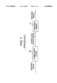
- FIG. 7 shows a schematic structure of a conventional receiver.
- a correlation process is applied to a received signal by a correlating filter 20 and then a decoding process is applied by a decoding circuit 21 to a correlated output signal where a correlation of a given condition is achieved, so that a decoded received signal is obtained.
- the correlating filter of this kind As a processing method achieved by the correlating filter of this kind, there have been a method where a correlation process is performed in an intermediate frequency band using a correlating filter including a SAW device and a method where a correlating filter is used for processing a base band signal after orthogonal detection.
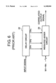
- FIG. 6 shows a schematic structure of a correlating filter of this kind.
- the correlating filter includes a delay circuit 22 and a weighted adder circuit 23.
- the correlating filter is provided, for example, before the decoding circuit 21 as shown in FIG. 7 so as to achieve a correlation relative to a base band signal.
- the delay circuit 22 is provided for outputting delayed signals relative to an input signal.
- the delay circuit 22 is constituted by, for example, a shift register.
- the delay circuit 22 is constituted by, for example, delay lines and an analog shift register.
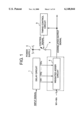
- FIG. 9 shows a known structure of an analog shift register.
- a plurality of sample hold circuits 24 having the same structure are coupled in cascade connection to each other, and each sample hold circuit is arranged to produce a delayed output.
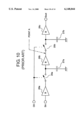
- FIG. 10 shows a known structure of the sample hold circuit 24.
- the sample hold circuit 24 includes switches 25a and 25b which are turned on and off synchronously with a clock signal (CK), buffer circuits 26a to 26c coupled in cascade connection to each other via the switches 25a and 25b, and capacitors 27a and 27b connected to input terminals of the buffer circuits 26b and 26c, respectively.
- CK clock signal
- the switches 25a and 25b are turned on at a leading edge (from low level to high level) of the clock signal and turned off at a trailing edge (from high level to low level) of the clock signal.
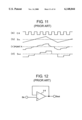
- an output signal Sout becomes a stepwise sampled signal as shown at (d) in FIG. 11.
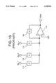
- FIG. 12 shows a known structure of the buffer circuit 26a to 26c, wherein a so-called voltage follower including an operational amplifier 28 is used.
- FIG. 13 shows another known structure of the buffer circuit 26a to 26c.
- a signal Sin is inputted to an inverted input terminal of an operational amplifier 28 via an impedance element 29a, and a feedback impedance element 29b is connected between the inverted input terminal and an output terminal of the operational amplifier 28 so as to form a so-called inverting amplifier.
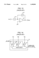
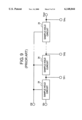
- FIG. 14 shows a known structure of the weighted adder circuit 23 (see FIG. 6).
- the weighted adder circuit 23 includes a plurality of weighting circuits 30 provided corresponding to tap outputs TP1 to TPn from the delay circuit 22 (see FIG. 6) and performing multiplication between the tap outputs TP1 to TPn and weighting coefficients W1 to Wn, and an adder circuit 31 which synthesizes output signals from the respective weighting circuits 30 to produce a correlated output signal.
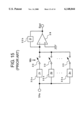
- the weighting circuit 30 When using a digital signal, it is preferable to constitute the weighting circuit 30 by a digital multiplier. On the other hand, when using an analog signal, it is preferable to constitute the weighting circuit 30 mainly by an operational amplifier 28 as shown in FIG. 15.
- the weighting circuit includes a plurality of impedance elements 32a provided corresponding to bits of a weighting coefficient in binary notation and a plurality of switches 33 provided corresponding to bits of a weighting coefficient in binary notation same as the impedance elements 32a.
- a plurality of impedance elements 32a provided corresponding to bits of a weighting coefficient in binary notation
- switches 33 provided corresponding to bits of a weighting coefficient in binary notation same as the impedance elements 32a.
- a non-inverted input terminal of the operational amplifier 28 is grounded, while a feedback impedance element 32b is connected between the inverted input terminal and an output terminal of the operational amplifier 28, so that an inverted amplification is achieved.
- ON/OFF states of the switches 33 are controlled corresponding to binary digits of the weighting coefficient.
- values of the impedance elements 32a are so set as to increase in order from the uppermost toward the lower impedance elements 32a. In other words, a value of the impedance element 32a connected to the switch 33 corresponding to the most significant bit is set to be minimum.
- Cf a capacitance of the capacitor as the feedback impedance element 32b
- an input signal TPin is weighted by the sum of the impedance elements 32a depending on the ON/OFF states of the switches 33 and, after amplification, outputted as a weighted output signal Eout.
- the adder circuit 31 (see FIG. 14) is preferably formed by a so-called digital adder when a digital signal is used. On the other hand, when using an analog signal, the adder circuit 31 is preferably formed by an analog adder as shown in FIG. 16.
- the analog adder is basically formed by an inverting amplifier including an operational amplifier 28. Specifically, a plurality of signals Sin 1 to Sin n are inputted to an inverted input terminal of the operational amplifier 28 via corresponding impedance elements 34 so that the inputted signals are added and an output signal Sout corresponding to an inverted value of the sum of the inputted signals are obtained.
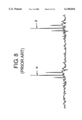
- the correlating filter 20 (see FIG. 7) having the foregoing structure is constantly inputted with the received signal and, when the received signal has a given correlation, the correlating filter 20 outputs a correlated output signal (see ⁇ , ⁇ in FIG. 8) with a large output level and a small output time width, similar to a so-called impulse signal.
- a correlated output signal see ⁇ , ⁇ in FIG. 8
- one largest correlated output signal is produced at a given position as corresponding to ⁇ or ⁇ in FIG. 8.
- signals with smaller levels than the correlated output signal are produced in the neighborhood thereof (see FIG. 8).
- the correlated output signal thus obtained is decoded in the decoding circuit 21 (see FIG. 7) so that a desired received signal is obtained.
- the signal necessary for decoding in the decoding circuit 21 corresponds to just the portions identified by ⁇ and ⁇ in FIG. 8 where the largest correlation peaks are achieved, so that the other portions are not necessary.
- the constant operation of the correlating filter is only required at a particular case, such as upon initial acquisition of synchronism or upon interference level measurement.
- the correlating filter for processing the base band signal after the orthogonal detection requires a relatively large number of the circuit parts as described above, so that the larger power consumption is required as compared with the other circuits. This can not be ignored particularly in a portable radio device using a battery as a power supply. Actually, such a correlating filter can not be used in the portable radio device.
- the foregoing conventional correlating filter using the SAW device requires a far greater mounting area on a printed board as compared with TV SAW filters or other semiconductor devices, so that reduction in size is very difficult. This raises a problem since such a correlating filter is not suitable for the portable radio device, particularly, using the CDMA communication system for which various practical techniques have been recently proposed.
- a correlating filter comprises delaying means for applying a delay process to an input signal and outputting a plurality of delayed signals having different delays; weighted adder means for weighting the plurality of delayed signals from the delaying means, respectively, and adding the weighted delayed signals; and operation control means for substantially stopping calculation of the weighted adder means during a time period other than when the weighted adder means outputs an output signal having a correlation peak.
- the invention has been made in view of the fact that the output signal having a so-called correlation peak is outputted from the weighted adder means for a relatively short time, and a signal required at a decoding circuit connected after the correlating filter is only the output signal having the correlation peak.
- the operation control means substantially stops calculation of the weighted adder means during a time period other than when the weighted adder means outputs the output signal having the correlation peak.
- a correlating filter comprises delaying means for applying a delay process to an input signal and outputting a plurality of delayed signals having different delays; weighted adder means for weighting the plurality of delayed signals from the delaying means, respectively, and adding the weighted delayed signals; and operation control means for enabling a power feed to the weighted adder means while the weighted adder means outputs an output signal having a correlation peak.
- the invention has been made in view of the fact that the output signal having a so-called correlation peak is outputted from the weighted adder means for a relatively short time, and a signal required at a decoding circuit connected after the correlating filter is only the output signal having the correlation peak.
- the operation control means stops the power feed to the weighted adder means during a time period other than when the weighted adder means outputs the output signal having the correlation peak.
- a correlating filter comprises delaying means for applying a delay process to an input signal and outputting a plurality of delayed signals having different delays; weighted adder means for weighting the plurality of delayed signals from the delaying means, respectively, and adding the weighted delayed signals; and switching means for inputting the delayed signals from the delaying means into the weighted adder means while the weighted adder means outputs an output signal having a correlation peak, while, otherwise, outputting a given value to the weighted adder means instead of the delayed signals from the delaying means.
- the invention has been made in view of the fact that the output signal having a so-called correlation peak is outputted from the weighted adder means for a relatively short time, and a signal required at a decoding circuit connected after the correlating filter is only the output signal having the correlation peak. While the switching means outputs the given value to the weighted adder means, the output signal from the weighted adder means has no correlation output so that the power consumption required for the calculation process in the weighted adder means is reduced as compared with the case where the correlation is achieved. Thus, the power consumption can be reduced.
- a correlating filter comprises delaying means for applying a delay process to an input signal and outputting a plurality of delayed signals having different delays; weighted adder means for weighting the plurality of delayed signals from the delaying means, respectively, and adding the weighted delayed signals; and switching means for inputting weighting coefficients from external into the weighted adder means while the weighted adder means outputs an output signal having a correlation peak, while, otherwise, outputting a given value to the weighted adder means instead of the weighting coefficients.
- the invention has been made in view of the fact that the output signal having a so-called correlation peak is outputted from the weighted adder means for a relatively short time, and a signal required at a decoding circuit connected after the correlating filter is only the output signal having the correlation peak. While the switching means outputs the given value, such as zero, to the weighted adder means, the output signal from the weighted adder means has no correlation output so that the power consumption required for the calculation process in the weighted adder means is reduced as compared with the case where the correlation is achieved. Thus, the power consumption can be reduced.
- a CDMA receiver comprises each of the foregoing correlating filters and decoding means for reproducing received data from an output signal of the correlating filter, wherein the decoding means is controlled by the operation control means of the correlating filter so as to be operated at the same timing as the weighted adder means.
- the invention has been made in view of the fact that the output signal having a so-called correlation peak is outputted from the weighted adder means for a relatively short time, and a signal required at a decoding circuit connected after the correlating filter is only the output signal having the correlation peak. Since the decoding means is controlled by the operation control means of the correlating filter so as to be operated at the same timing as the weighted adder means, not only the weighted adder means, but also the decoding means can reduce the power consumption.
- FIG. 1 is a structural diagram showing a correlating filter according to a first preferred embodiment of the present invention
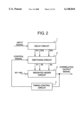
- FIG. 2 is a structural diagram showing a correlating filter according to a second preferred embodiment of the present invention.
- FIG. 3 is a structural diagram showing a correlating filter according to a third preferred embodiment of the present invention.
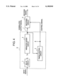
- FIG. 4 is a structural diagram showing a CDMA receiver according to a preferred embodiment of the present invention.
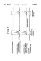
- FIG. 5 is a timing chart for explaining an operation of the correlating filter according to the first preferred embodiment of the present invention.
- FIG. 6 is a structural diagram showing an example of a conventional correlating filter
- FIG. 7 is a structural diagram showing an example of a conventional CDMA receiver
- FIG. 8 is a schematic diagram for explaining a state of an output signal of a conventional correlating filter
- FIG. 9 is a structural diagram showing an example of a conventional delay circuit
- FIG. 10 is a structural diagram showing an example of a conventional sample hold circuit
- FIG. 11 is a timing chart for explaining an operation of the sample hold circuit shown in FIG. 10;
- FIG. 12 is a structural diagram showing an example of a conventional buffer circuit
- FIG. 13 is a structural diagram showing another example of a conventional buffer circuit
- FIG. 14 is a structural diagram showing an example of a conventional weighted adder circuit
- FIG. 15 is a structural diagram showing an example of a conventional weighting circuit.
- FIG. 16 is a structural diagram showing an example of a conventional synthesizing circuit.
- the correlating filter includes a delay circuit 1, a weighted adder circuit 2, a timing control circuit 3 and a switching element 4.
- the delay circuit 1 and the weighted adder circuit 2 are basically the same as those of the conventional correlating filter.
- the timing control circuit 3 controls an operation of the switching element 4 based on a correlated output signal obtained from the weighted adder circuit 2.
- the switching element 4 is turned on at given time intervals so as to apply the power supply voltage to the weighted adder circuit 2 from the power supply 5.
- a signal inputted to the delay circuit 1 is delayed so as to be outputted as a plurality of tap output signals TP1 to TPn having different delays, and then inputted to the weighted adder circuit 2. This is the same as the prior art.
- the weighted adder circuit 2 produces a correlated output signal as shown at (b) in FIG. 5, with respect to the tap output signals TP1 to TPn inputted from the delay circuit 1. This is also the same as the prior art.
- the timing control circuit 3 based on the output signal from the weighed adder circuit 2, the timing control circuit 3 produces a control signal as shown, for example, at (a) in FIG. 5, which becomes high in level in a period where the largest correlation peaks are concentrated.
- the switching element 4 is connected in series between a power supply section (not shown) of the weighted adder circuit 2 and the power supply 5, and turned on only when the control signal from the timing control circuit 3 (see FIG. 5(a)) is high in level. Thus, the weighted adder circuit 2 is fed with the power only during this period so as to be operated.
- the timing of the control signal to become high in level is not determined in advance.
- the timing control circuit 3 for example, outputs a control signal which can turn on the switching element 4 at given time intervals so as to operate the weighted adder circuit 2. Then, based on an output signal from the weighted adder circuit 2, the timing control circuit 3 determines whether the largest correlation peak appears or not, so as to finally produce the control signal as shown at (a) in FIG. 5.
- the power consumption is not generated in the weighted adder circuit 2 during time periods other than when the switching element 4 is turned on based on the control signal.
- the power saving can be achieved as seen from (c) in FIG. 5.
- the mean power is represented by a ratio derived by the following equation:
- the derived value represents that the power consumption can be suppressed to 19% relative to the conventional power consumption caused by the constant power feed.
- a chain line represents the mean power consumption, while a solid line represents the power consumption when the largest correlated output signal is outputted from the weighted adder circuit 2 and decoded at a decoding circuit (not shown).
- the delay circuit 1 corresponds to delay means in claim 1 and 2
- the weighted adder circuit 2 corresponds to weighted adder means in claim land 2
- the timing control circuit 3 and the switching element 4 correspond to operation control means in claim 1 and 2 respectively.
- FIG. 2 the same elements as those in FIG. 1 are assigned the same reference marks so as to omit detailed explanation thereof
- a switching circuit 6 is provided between the delay circuit 1 and the weighted adder circuit 2.
- the switching circuit 6 is operated depending on a control signal from the timing control circuit 3.
- the switching circuit 6 in response to the control signal as shown at (a) in FIG. 5 inputted from the timing control circuit 3, the switching circuit 6 outputs the tap output signals TPl to TPn from the delay circuit 1 to the weighted adder circuit 2 only when the inputted signal has a correlation peak, as shown in FIG. 1 so that the control signal is high in level, while, otherwise, the switching circuit 6 outputs a given value to the weighted adder circuit 2.
- the given value outputted from the switching circuit 6 is set to be a fixed value which provides no correlation output in the correlated output signal from the weighted adder circuit 2. Accordingly, while this fixed value is inputted, the power consumption at the weighted adder circuit 2 is smaller than that when the correlation peak appears, and further approximately constant.
- the switching circuit 6 can be formed by so-called gate elements, such as AND circuits or OR circuits, when handling a digital signal.
- the switching circuit 6 can be formed by an analog switch or the like so as to switch between the output signals from the delay circuit 1 and the foregoing fixed value. In such structures, particularly, the effect in reduction of power consumption in a digital circuit using CMOS or the like is significant.
- the delay circuit 1 corresponds to delay means in claim 1 and 3
- the weighted adder circuit 2 corresponds to weighted adder means in claim 1 and 3
- the timing control circuit 3 and the switching circuit 6 correspond to operation control means in claim 1 and switching means in claim 3 respectively.
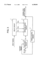
- FIG. 3 the same elements as those in FIG. 1 or 2 are assigned the same reference marks so as to omit detailed explanation thereof.
- the correlating filter includes the delay circuit 1 and the weighted adder circuit 2 and fierier includes a switching circuit 7 for switching the weighting coefficients used in weighted adder circuit 2 and the timing control circuit 3 for controlling an operation timing of the switching circuit 7.
- the switching circuit 7 outputs the weighting coefficients W1 to Wn, inputted from the external, directly to the weighted adder circuit 2 only when the inputted signal has a correlation peak, while, otherwise, the switching circuit 7 outputs a value of zero to the weighted adder circuit 2 as the weight coefficients.
- the timing control circuit 3 Based on correlation output signal inputted from the weighted adder circuit 2, when the inputted signal has a correlation, the timing control circuit 3, for example, outputs control signal as shown at (a) in FIG. 5.
- the timing control circuit 3 is basically the same as shown in FIG. 1 and 2.
- the switching circuit 7 In response to the control signal as shown at (a) in FIG. 5 inputted from the timing control circuit 3, the switching circuit 7 outputs the weighting coefficients W1 to Wn, inputted from the external, directly to the weighted adder circuit 2 only when the inputted signal has a correlation peak, as shown in FIG. 1 so that the control signal is high in level, while, otherwise, the switching circuit 7 outputs a value of zero to the weighted adder circuit 2 instead of the weighting coefficients W1 to Wn.
- the weighting calculation is performed at the weighted adder circuit 2.
- the rate of reduction in power consumption is smaller as compared with the second preferred embodiment.
- adding of the calculated results after the weighting calculation is not performed, the reduction in power consumption corresponding thereto is reliably achieved.
- the weighted adder circuit is constituted by a digital circuit using CMOS or the like, the effect of reduction in power consumption is significant.
- the delay circuit 1 corresponds to delay means in claim 1 and 4
- the weighted adder circuit 2 corresponds to weighted adder means in claim land 4
- the timing control circuit 3 and the switching circuit 7 correspond to operation control means in claim 1 and switching means in claim 4 respectively.
- FIG. 4 the same elements as those in FIG. 1, 2 or 3 are assigned the same reference marks so as to omit detailed explanation thereof
- the CDMA receiver includes a correlating filter 8 and a decoding circuit 9.
- the correlating filter 8 may have any one of the structures shown in FIGS. 1 to 3.
- the correlating filter 8 is shown to have only the three circuits (the delay circuit 1, the weighted adder circuit 2 and the timing control circuit 3) which are common to all the correlating filters shown in FIGS. 1 to 3, for simplicity.
- a control signal from the timing control circuit 3 is supplied not only within the correlating filter 8, but also to the decoding circuit 9 so as to control an operation thereof.
- the decoding circuit 9 is operated only when the control signal is high in level, to perform the decoding process so that a decoded signal is obtained.
- the calculating operation of the weighted adder means is substantially stopped during a time period where no such a calculating operation is necessary, the reduction in power consumption is achieved.
- the correlating filter which can be used in the portable device is provided.
- the correlating filter in the first preferred embodiment of the present invention since the power feed to the weighted adder means is performed only during a time period where the power feed is actually necessary, the power consumption which is actually not required is prevented from occurring. Thus, the reduction in power consumption is achieved and, in particular, the correlating filter which can be used in the portable device is provided.
- the weighted adder means is inputted with the constant value instead of the input signals from the delaying means during a time period where the calculating process by the weighted adder means is not necessary, the power consumption required for the calculating process in the weighted adder means is reduced.
- the reduction in power consumption is achieved and, in particular, the correlating filter which can be used in the portable device is provided.
- the correlating filter in the third preferred embodiment of the present invention since the weighted adder means is inputted with the constant value instead of the weighting coefficients from the external during a time period where the calculating process by the weighted adder means is not necessary, the power consumption required for the calculating process in the weighted adder means is reduced. Thus, the reduction in power consumption is achieved and, in particular, the correlating filter which can be used in the portable device is provided.
- the reduction in power consumption in the correlating filter is achieved as described above and, in addition, since the decoding means is operated only while the signal having the correlation peak is received from the correlating filter, the reduction in power consumption is also achieved in the decoding means comparing with conventional decoding means that is constantly operated.
- the CDMA receiver suitable for the portable device can be provided.
Landscapes
- Filters That Use Time-Delay Elements (AREA)
- Noise Elimination (AREA)
- Networks Using Active Elements (AREA)
Applications Claiming Priority (2)
| Application Number | Priority Date | Filing Date | Title |
|---|---|---|---|
| JP8-005235 | 1996-01-16 | ||
| JP523596A JP3269959B2 (ja) | 1996-01-16 | 1996-01-16 | 相関フィルタ及びcdma受信装置 |
Publications (1)
| Publication Number | Publication Date |
|---|---|
| US6148044A true US6148044A (en) | 2000-11-14 |
Family
ID=11605540
Family Applications (1)
| Application Number | Title | Priority Date | Filing Date |
|---|---|---|---|
| US08/783,093 Expired - Lifetime US6148044A (en) | 1996-01-16 | 1997-01-14 | Correlating filter and CDMA receiver |
Country Status (4)
| Country | Link |
|---|---|
| US (1) | US6148044A (de) |
| EP (1) | EP0785621B1 (de) |
| JP (1) | JP3269959B2 (de) |
| DE (1) | DE69712807T2 (de) |
Cited By (5)
| Publication number | Priority date | Publication date | Assignee | Title |
|---|---|---|---|---|
| US20010038667A1 (en) * | 2000-05-01 | 2001-11-08 | Kenzo Urabe | Matched filter and receiver for mobile radio communication system |
| US6507603B1 (en) * | 1998-09-07 | 2003-01-14 | Fujitsu Limited | CDMA receiver |
| US6693953B2 (en) * | 1998-09-30 | 2004-02-17 | Skyworks Solutions, Inc. | Adaptive wireless communication receiver |
| US20080192863A1 (en) * | 2007-02-14 | 2008-08-14 | Wilinx Inc. | Systems and methods for synchronizing wireless communication systems |
| US9160575B1 (en) * | 2014-09-24 | 2015-10-13 | Realtek Semiconductor Corporation | Discrete-time linear equalizer and method thereof |
Families Citing this family (4)
| Publication number | Priority date | Publication date | Assignee | Title |
|---|---|---|---|---|
| JP3199039B2 (ja) | 1998-11-02 | 2001-08-13 | 日本電気株式会社 | 消費電力低減回路及びこれを用いた無線通信装置並びに無線通信装置における消費電力低減方法 |
| JP3367475B2 (ja) | 1999-07-06 | 2003-01-14 | 日本電気株式会社 | 無線通信機および無線通信機の消費電力制御方法 |
| US6674397B2 (en) * | 2002-05-13 | 2004-01-06 | Honeywell International Inc. | Methods and apparatus for minimum computation phase demodulation |
| JP2006339967A (ja) * | 2005-06-01 | 2006-12-14 | Samsung Electronics Co Ltd | 無線受信機 |
Citations (3)
| Publication number | Priority date | Publication date | Assignee | Title |
|---|---|---|---|---|
| US4217586A (en) * | 1977-05-16 | 1980-08-12 | General Electric Company | Channel estimating reference signal processor for communication system adaptive antennas |
| US5151919A (en) * | 1990-12-17 | 1992-09-29 | Ericsson-Ge Mobile Communications Holding Inc. | Cdma subtractive demodulation |
| US5574747A (en) * | 1995-01-04 | 1996-11-12 | Interdigital Technology Corporation | Spread spectrum adaptive power control system and method |
Family Cites Families (8)
| Publication number | Priority date | Publication date | Assignee | Title |
|---|---|---|---|---|
| JPH02261226A (ja) * | 1989-03-31 | 1990-10-24 | Mitsubishi Electric Corp | 移動電話機 |
| JP2888782B2 (ja) * | 1995-09-08 | 1999-05-10 | エヌ・ティ・ティ移動通信網株式会社 | 通信のためのフィルタ回路 |
| JPH06181424A (ja) * | 1992-12-14 | 1994-06-28 | Kawasaki Steel Corp | ディジタルフィルタシステム |
| JPH06252887A (ja) * | 1993-03-01 | 1994-09-09 | Toyo Commun Equip Co Ltd | スペクトラム拡散信号復調装置 |
| JPH0795126A (ja) * | 1993-09-22 | 1995-04-07 | Sony Corp | 受信装置 |
| WO1995010903A1 (en) * | 1993-10-14 | 1995-04-20 | Ntt Mobile Communications Network Inc. | Correlation detector and communication apparatus |
| JP2700000B2 (ja) * | 1995-05-10 | 1998-01-19 | 日本電気株式会社 | 無線lanシステムの無線送受信機 |
| JPH09116465A (ja) * | 1995-10-16 | 1997-05-02 | Kokusai Electric Co Ltd | スペクトル拡散通信用相関器 |
-
1996
- 1996-01-16 JP JP523596A patent/JP3269959B2/ja not_active Expired - Fee Related
-
1997
- 1997-01-14 US US08/783,093 patent/US6148044A/en not_active Expired - Lifetime
- 1997-01-16 EP EP19970100621 patent/EP0785621B1/de not_active Expired - Lifetime
- 1997-01-16 DE DE69712807T patent/DE69712807T2/de not_active Expired - Fee Related
Patent Citations (3)
| Publication number | Priority date | Publication date | Assignee | Title |
|---|---|---|---|---|
| US4217586A (en) * | 1977-05-16 | 1980-08-12 | General Electric Company | Channel estimating reference signal processor for communication system adaptive antennas |
| US5151919A (en) * | 1990-12-17 | 1992-09-29 | Ericsson-Ge Mobile Communications Holding Inc. | Cdma subtractive demodulation |
| US5574747A (en) * | 1995-01-04 | 1996-11-12 | Interdigital Technology Corporation | Spread spectrum adaptive power control system and method |
Cited By (10)
| Publication number | Priority date | Publication date | Assignee | Title |
|---|---|---|---|---|
| US6507603B1 (en) * | 1998-09-07 | 2003-01-14 | Fujitsu Limited | CDMA receiver |
| US6693953B2 (en) * | 1998-09-30 | 2004-02-17 | Skyworks Solutions, Inc. | Adaptive wireless communication receiver |
| US20010038667A1 (en) * | 2000-05-01 | 2001-11-08 | Kenzo Urabe | Matched filter and receiver for mobile radio communication system |
| US7003022B2 (en) * | 2000-05-01 | 2006-02-21 | Telefonaktiebolaget L M Ericsson (Publ) | Matched filter and receiver for mobile radio communication system |
| US20080192863A1 (en) * | 2007-02-14 | 2008-08-14 | Wilinx Inc. | Systems and methods for synchronizing wireless communication systems |
| US7693237B2 (en) * | 2007-02-14 | 2010-04-06 | Wilinx Corporation | Systems and methods for synchronizing wireless communication systems |
| US9160575B1 (en) * | 2014-09-24 | 2015-10-13 | Realtek Semiconductor Corporation | Discrete-time linear equalizer and method thereof |
| CN105450567A (zh) * | 2014-09-24 | 2016-03-30 | 瑞昱半导体股份有限公司 | 线性均衡器 |
| TWI580232B (zh) * | 2014-09-24 | 2017-04-21 | 瑞昱半導體股份有限公司 | 線性等化器 |
| CN105450567B (zh) * | 2014-09-24 | 2018-09-04 | 瑞昱半导体股份有限公司 | 线性均衡器 |
Also Published As
| Publication number | Publication date |
|---|---|
| JP3269959B2 (ja) | 2002-04-02 |
| JPH09200177A (ja) | 1997-07-31 |
| EP0785621B1 (de) | 2002-05-29 |
| DE69712807D1 (de) | 2002-07-04 |
| DE69712807T2 (de) | 2003-01-16 |
| EP0785621A1 (de) | 1997-07-23 |
Similar Documents
| Publication | Publication Date | Title |
|---|---|---|
| US6366765B1 (en) | Receiver | |
| US6148044A (en) | Correlating filter and CDMA receiver | |
| EP2321899A1 (de) | Verfahren und schaltkreis zur verzerrungsminderung bei einem leistungsverstärker | |
| US7251268B2 (en) | Rake receiver | |
| US4668989A (en) | Fading circuit for video signals | |
| US5414311A (en) | Sample and hold circuit and finite impulse response filter constructed therefrom | |
| US4727504A (en) | Interference canceller and signal quantizer | |
| US6031415A (en) | Matched filter circuit for spread spectrum communication | |
| WO1996021975A1 (en) | Method and apparatus for determining a masked threshold | |
| US6263012B1 (en) | Receiver apparatus for CDMA communication system | |
| CA2279680C (en) | Binary waveform shaping apparatus | |
| EP0940916A2 (de) | Filterschaltung | |
| US6983012B1 (en) | Implementation of digital filter with reduced hardware | |
| US5101370A (en) | Programmable digital accumulate and scale circuit | |
| US7099907B1 (en) | Fir filter and ramp-up/-down control circuit using the same | |
| US7671644B2 (en) | Process insensitive delay line | |
| US6256341B1 (en) | Spread spectrum receiver using digital matched filter | |
| US6768372B2 (en) | Analog filter architecture | |
| JP3503409B2 (ja) | スペクトル拡散受信機 | |
| US6141761A (en) | Low power consuming operating device for digital signal processing using a probability distribution of input digital signals and predetermined output signals | |
| KR100678566B1 (ko) | 진폭 검출 회로 | |
| KR0149323B1 (ko) | 디지탈 방식의 오디오 음량 조절장치 | |
| KR100353718B1 (ko) | 코드분할다중접속 휴대용 무선단말기의 혼변조 특성 개선장치 | |
| CN101015183B (zh) | 用于将数字基带信号转换成模拟中频信号的方法 | |
| KR20010046767A (ko) | 의사잡음 코드 발생 방법 |
Legal Events
| Date | Code | Title | Description |
|---|---|---|---|
| AS | Assignment |
Owner name: KOKUSAI ELECTRIC CO., JAPAN Free format text: ASSIGNMENT OF ASSIGNORS INTEREST;ASSIGNORS:ONO, HIROKO;TAKADA, MASATOSHI;URABE, KENZO;REEL/FRAME:008670/0491 Effective date: 19961229 |
|
| STCF | Information on status: patent grant |
Free format text: PATENTED CASE |
|
| FPAY | Fee payment |
Year of fee payment: 4 |
|
| FEPP | Fee payment procedure |
Free format text: PAYOR NUMBER ASSIGNED (ORIGINAL EVENT CODE: ASPN); ENTITY STATUS OF PATENT OWNER: LARGE ENTITY |
|
| FPAY | Fee payment |
Year of fee payment: 8 |
|
| FPAY | Fee payment |
Year of fee payment: 12 |