US5981361A - Fabrication process of a semiconductor device including a dicing process of a semiconductor wafer - Google Patents
Fabrication process of a semiconductor device including a dicing process of a semiconductor wafer Download PDFInfo
- Publication number
- US5981361A US5981361A US08/927,209 US92720997A US5981361A US 5981361 A US5981361 A US 5981361A US 92720997 A US92720997 A US 92720997A US 5981361 A US5981361 A US 5981361A
- Authority
- US
- United States
- Prior art keywords
- adhesive tape
- semiconductor
- curing
- semiconductor substrate
- sawing
- Prior art date
- Legal status (The legal status is an assumption and is not a legal conclusion. Google has not performed a legal analysis and makes no representation as to the accuracy of the status listed.)
- Expired - Lifetime
Links
Images


Classifications
-
- H—ELECTRICITY
- H01—ELECTRIC ELEMENTS
- H01L—SEMICONDUCTOR DEVICES NOT COVERED BY CLASS H10
- H01L21/00—Processes or apparatus adapted for the manufacture or treatment of semiconductor or solid state devices or of parts thereof
- H01L21/67—Apparatus specially adapted for handling semiconductor or electric solid state devices during manufacture or treatment thereof; Apparatus specially adapted for handling wafers during manufacture or treatment of semiconductor or electric solid state devices or components ; Apparatus not specifically provided for elsewhere
- H01L21/683—Apparatus specially adapted for handling semiconductor or electric solid state devices during manufacture or treatment thereof; Apparatus specially adapted for handling wafers during manufacture or treatment of semiconductor or electric solid state devices or components ; Apparatus not specifically provided for elsewhere for supporting or gripping
- H01L21/6835—Apparatus specially adapted for handling semiconductor or electric solid state devices during manufacture or treatment thereof; Apparatus specially adapted for handling wafers during manufacture or treatment of semiconductor or electric solid state devices or components ; Apparatus not specifically provided for elsewhere for supporting or gripping using temporarily an auxiliary support
- H01L21/6836—Wafer tapes, e.g. grinding or dicing support tapes
-
- H—ELECTRICITY
- H01—ELECTRIC ELEMENTS
- H01L—SEMICONDUCTOR DEVICES NOT COVERED BY CLASS H10
- H01L21/00—Processes or apparatus adapted for the manufacture or treatment of semiconductor or solid state devices or of parts thereof
- H01L21/70—Manufacture or treatment of devices consisting of a plurality of solid state components formed in or on a common substrate or of parts thereof; Manufacture of integrated circuit devices or of parts thereof
- H01L21/77—Manufacture or treatment of devices consisting of a plurality of solid state components or integrated circuits formed in, or on, a common substrate
- H01L21/78—Manufacture or treatment of devices consisting of a plurality of solid state components or integrated circuits formed in, or on, a common substrate with subsequent division of the substrate into plural individual devices
-
- H—ELECTRICITY
- H01—ELECTRIC ELEMENTS
- H01L—SEMICONDUCTOR DEVICES NOT COVERED BY CLASS H10
- H01L2221/00—Processes or apparatus adapted for the manufacture or treatment of semiconductor or solid state devices or of parts thereof covered by H01L21/00
- H01L2221/67—Apparatus for handling semiconductor or electric solid state devices during manufacture or treatment thereof; Apparatus for handling wafers during manufacture or treatment of semiconductor or electric solid state devices or components; Apparatus not specifically provided for elsewhere
- H01L2221/683—Apparatus for handling semiconductor or electric solid state devices during manufacture or treatment thereof; Apparatus for handling wafers during manufacture or treatment of semiconductor or electric solid state devices or components; Apparatus not specifically provided for elsewhere for supporting or gripping
- H01L2221/68304—Apparatus for handling semiconductor or electric solid state devices during manufacture or treatment thereof; Apparatus for handling wafers during manufacture or treatment of semiconductor or electric solid state devices or components; Apparatus not specifically provided for elsewhere for supporting or gripping using temporarily an auxiliary support
- H01L2221/68327—Apparatus for handling semiconductor or electric solid state devices during manufacture or treatment thereof; Apparatus for handling wafers during manufacture or treatment of semiconductor or electric solid state devices or components; Apparatus not specifically provided for elsewhere for supporting or gripping using temporarily an auxiliary support used during dicing or grinding
-
- H—ELECTRICITY
- H01—ELECTRIC ELEMENTS
- H01L—SEMICONDUCTOR DEVICES NOT COVERED BY CLASS H10
- H01L2221/00—Processes or apparatus adapted for the manufacture or treatment of semiconductor or solid state devices or of parts thereof covered by H01L21/00
- H01L2221/67—Apparatus for handling semiconductor or electric solid state devices during manufacture or treatment thereof; Apparatus for handling wafers during manufacture or treatment of semiconductor or electric solid state devices or components; Apparatus not specifically provided for elsewhere
- H01L2221/683—Apparatus for handling semiconductor or electric solid state devices during manufacture or treatment thereof; Apparatus for handling wafers during manufacture or treatment of semiconductor or electric solid state devices or components; Apparatus not specifically provided for elsewhere for supporting or gripping
- H01L2221/68304—Apparatus for handling semiconductor or electric solid state devices during manufacture or treatment thereof; Apparatus for handling wafers during manufacture or treatment of semiconductor or electric solid state devices or components; Apparatus not specifically provided for elsewhere for supporting or gripping using temporarily an auxiliary support
- H01L2221/68354—Apparatus for handling semiconductor or electric solid state devices during manufacture or treatment thereof; Apparatus for handling wafers during manufacture or treatment of semiconductor or electric solid state devices or components; Apparatus not specifically provided for elsewhere for supporting or gripping using temporarily an auxiliary support used to support diced chips prior to mounting
-
- Y—GENERAL TAGGING OF NEW TECHNOLOGICAL DEVELOPMENTS; GENERAL TAGGING OF CROSS-SECTIONAL TECHNOLOGIES SPANNING OVER SEVERAL SECTIONS OF THE IPC; TECHNICAL SUBJECTS COVERED BY FORMER USPC CROSS-REFERENCE ART COLLECTIONS [XRACs] AND DIGESTS
- Y10—TECHNICAL SUBJECTS COVERED BY FORMER USPC
- Y10S—TECHNICAL SUBJECTS COVERED BY FORMER USPC CROSS-REFERENCE ART COLLECTIONS [XRACs] AND DIGESTS
- Y10S438/00—Semiconductor device manufacturing: process
- Y10S438/977—Thinning or removal of substrate
-
- Y—GENERAL TAGGING OF NEW TECHNOLOGICAL DEVELOPMENTS; GENERAL TAGGING OF CROSS-SECTIONAL TECHNOLOGIES SPANNING OVER SEVERAL SECTIONS OF THE IPC; TECHNICAL SUBJECTS COVERED BY FORMER USPC CROSS-REFERENCE ART COLLECTIONS [XRACs] AND DIGESTS
- Y10—TECHNICAL SUBJECTS COVERED BY FORMER USPC
- Y10T—TECHNICAL SUBJECTS COVERED BY FORMER US CLASSIFICATION
- Y10T29/00—Metal working
- Y10T29/51—Plural diverse manufacturing apparatus including means for metal shaping or assembling
- Y10T29/5102—Binding or covering and cutting
-
- Y—GENERAL TAGGING OF NEW TECHNOLOGICAL DEVELOPMENTS; GENERAL TAGGING OF CROSS-SECTIONAL TECHNOLOGIES SPANNING OVER SEVERAL SECTIONS OF THE IPC; TECHNICAL SUBJECTS COVERED BY FORMER USPC CROSS-REFERENCE ART COLLECTIONS [XRACs] AND DIGESTS
- Y10—TECHNICAL SUBJECTS COVERED BY FORMER USPC
- Y10T—TECHNICAL SUBJECTS COVERED BY FORMER US CLASSIFICATION
- Y10T29/00—Metal working
- Y10T29/51—Plural diverse manufacturing apparatus including means for metal shaping or assembling
- Y10T29/5193—Electrical connector or terminal
Definitions
- the present invention generally relates to fabrication of semiconductor devices and more particularly to a fabrication process of a semiconductor device including a dicing process of a semiconductor wafer and an apparatus therefor.
- a dicing process it is commonly practiced to protect the semiconductor wafer, on which semiconductor devices are already formed, by an adhesive tape, such that the semiconductor devices are not damaged by the sawing process achieved by a dicing saw.
- the sawing may be conducted such that the depth of the dicing grooves, formed as a result of the action of the dicing saw, exceeds the thickness of the semiconductor wafer (full-cut dicing), or alternatively such that the depth of the dicing grooves is smaller than the wafer thickness (semi-full-cut dicing).
- a cleaning process is conducted for removing dust particles formed as a result of the sawing, by applying a jet of a cleaning liquid such as water. Further, a first drying process is conducted immediately after the cleaning process for eliminating the cleaning liquid by applying an air jet.
- the conventional fabrication process of semiconductor devices has suffered from the problem of low throughput of production, primarily due to the existence of the second drying process in the dicing process.
- the adhesive tape remains sticky in correspondence to the part of the tape where the dicing grooves are formed, and the semiconductor chips may carry uncured, sticky adhesives thereon when the chips are picked up from the tape.
- the yield of production of the semiconductor device in the later process, such as the packaging process may be deteriorated.
- Another and more specific object of the present invention is to provide a fabrication process of a semiconductor device that can successfully reduce the time, and hence cost, needed for a dicing process for dividing a semiconductor wafer into individual semiconductor chips.
- Another object of the present invention is to provide a method of improving the yield of production of semiconductor devices, by eliminating the damaging of semiconductor chips that may occur in a dicing process when transporting the semiconductor chips, divided from a common semiconductor wafer in the dicing process, from a sawing unit to a UV-curing unit in the state that the semiconductor chips are held on a flexible adhesive tape.
- Another object of the present invention is to provide a method of fabricating a semiconductor device, comprising the steps of:
- step of applying said dry gas, said step of applying said infrared radiation and said step of curing said adhesive layer being conducted substantially simultaneously.
- a lamp house body surrounding said ultraviolet radiation source, said lamp house body carrying a mirror surface;
- said lamp house body an opening provided on said lamp house body, said opening being adapted for supporting semiconductor chips arranged on an adhesive tape;
- an air nozzle disposed such that said air nozzle applies a dry gas to said semiconductor substrate held on said opening.
- the drying process for eliminating water or moisture from the part of the adhesive tape corresponding to the dicing grooves is conducted substantially concurrently to the curing process of the ultraviolet-curing resin, and the throughput of production of the semiconductor devices is improved substantially.
- the curing of the adhesive layer is thus conducted in a dry environment substantially free from water or moisture, the curing of the adhesive layer proceeds completely and the problem of decreased yield of the semiconductor device production, caused as a result of the partially cured adhesive layer sticking to the semiconductor chips, is successfully and effectively avoided.
- the sawing of the semiconductor substrate is conducted in the state that the semiconductor substrate is protected by the adhesive tape, mechanical damage to the semiconductor chips is minimized during the dicing process.
- Another object of the present invention is to provide an apparatus for fabricating a semiconductor device, comprising:
- a lamp house body surrounding said ultraviolet radiation source, said lamp house body carrying a mirror surface;
- a vacuum chuck provided on said lamp house body so as to cover said opening, said vacuum chuck being adapted for supporting a semiconductor substrate thereon in a state that said semiconductor substrate is covered by said adhesive tape;
- said vacuum chuck being formed of a material substantially transparent to an ultraviolet radiation produced by said ultraviolet radiation source.
- the dicing of the semiconductor substrate is carried out on the lamp house of the ultraviolet radiation source.
- FIG. 1 is a diagram showing the construction of a dicing apparatus according to a first embodiment of the present invention
- FIG. 2 is a diagram showing the construction of a dicing apparatus according to a second embodiment of the present invention.
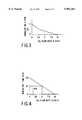
- FIG. 3 is a diagram showing the relationship between the amount of the adhesives sticking to a semiconductor chip and the flow rate of a dry N 2 gas applied in a curing unit of FIG. 1 or FIG. 2;
- FIG. 4 is a diagram showing the relationship between the time needed for drying a wafer and the flow rate of a dry N 2 gas applied in the curing unit of FIG. 1 or FIG. 2;
- FIG. 5A and 5B are diagrams explaining the problem that occurs when transporting semiconductor chips together with an adhesive tape
- FIG. 6 is a diagram showing the construction of a dicing apparatus according to a third embodiment of the present invention in a sawing step
- FIG. 7 is a diagram showing the construction of a dicing apparatus according to a third embodiment of the present invention in a curing step.
- FIG. 8 is a diagram showing the absorption spectrum of Al 2 O 3 .
- FIG. 1 shows the construction of a dicing apparatus 1 used in a first embodiment of the present invention for dicing a semiconductor wafer.
- the dicing apparatus 1 includes a sawing unit 2 for sawing a semiconductor wafer 4 in the state that the semiconductor wafer 4 is protected by an adhesive tape 6, and a curing unit 3 for curing an adhesive layer 6" on the adhesive tape 6, by applying an ultraviolet radiation thereto.
- the adhesive tape 6 includes, in addition to the foregoing adhesive layer 6", a tape base 6' of typically a polyvinyl chloride resin or a polyolefin resin.
- the sawing unit 2 includes a dicing table carrying thereon a vacuum chuck 7, wherein the vacuum chuck 7 is adapted to hold thereon the semiconductor wafer 4 in a state that the semiconductor wafer 4 is covered by the adhesive tape 6, by applying a vacuum to the tape 6.
- the vacuum chuck 7 On the vacuum chuck 7, there is disposed a rotary dicing saw 8 and a cooling water nozzle 17 that applies a cooling liquid 18 to the dicing saw 8 as well as to the semiconductor wafer 4.
- the tape 6 is mounted on the vacuum chuck 7 in a state that the tape 6 is tensioned on a frame 5 firmly.
- the dicing saw 8 is rotated at a high speed, and the dicing table is moved back and forth together with the vacuum chuck 7 thereon, as indicated by arrows in FIG. 1.
- the dicing saw 8 is moved in the back and forth directions.
- the vacuum chuck 7 is rotatable together with the dicing table as indicated by arrows in FIG. 1.
- the dicing saw 8 is movable vertically in the upward and downward directions as indicated in FIG. 1 by arrows.
- the wafer 4 is cut by the dicing saw 8 along the predetermined scribe lines, and there are formed dicing grooves in the semiconductor wafer 4 in correspondence to the scribe lines.
- the surface of the adhesive tape, on which the adhesive layer is formed is exposed as a result of the formation of the dicing grooves.
- the semiconductor chips thus formed are held on the tape 6 in the desired row and column formation as a result of the adherence of the adhesive tape 6, and the problem of scattering of the semiconductor chips is successfully avoided.
- the dicing saw 8 is cooled by the cooling liquid 18 sprayed upon the dicing saw 8 from the spray nozzle 17 as noted previously, wherein a purified water or a diluted soda water may be used for the cooling liquid 18.
- the cooling liquid 18 not only cools the dicing saw 8 but also the semiconductor wafer 4. Further, the cooling liquid 18 washes away the dust particles that are formed as a result of the sawing of the semiconductor wafer 4.
- the curing unit 3 on the other hand, includes a UV lamp 13 that emits a UV radiation 12 and a lamp house 16 that carries a mirror surrounding the lamp 13.
- the lamp house 16 further includes an opening for emitting the UV radiation produced by the UV lamp 13 to the exterior of the lamp house 16.
- the adhesive tape 6 held on the frame 5 is dismounted, after the sawing of the semiconductor wafer 4 is completed, from the vacuum chuck 7 of the sawing unit 2 by a carrier mechanism not illustrated.
- the adhesive tape 6 thus dismounted carries thereon the semiconductor chips formed as a result of the sawing process and is accommodated into a cassette not illustrated.
- the cassette is then transported to the curing unit 3 by a robot, and the adhesive tape 6 held by the frame 5 is mounted on the foregoing opening of the lamp house 16.
- the tape 6 thus mounted on the opening of the lamp house 16 carries thereon the semiconductor chips formed as a result of the sawing process, as noted already, wherein the semiconductor chips on the tape 6 are held in the state that the chips are separated from each other by dicing grooves 9.
- the adhesive layer 6" of the tape 6 is exposed in correspondence to the dicing grooves 9.
- the lamp house 16 of the curing unit 3 includes an infrared lamp 15 emitting an infrared radiation 14 adjacent to the UV lamp 13.
- the infrared lamp 15 emitting an infrared radiation 14 adjacent to the UV lamp 13.
- FIG. 1 includes, in addition to the infrared lamp 15, an air nozzle 11 above the lamp house 16 such that the air nozzle 11 faces the tape 6 in a state that the tape 6, carrying thereon the semiconductor chips, is mounted on the foregoing opening of the lamp house 16.
- the air nozzle 11 thereby applies a dry gas 10 preferably a dry inert gas such as N 2 or alternatively a dry air to the tape 6 for facilitating the removal of water or moisture from the dicing grooves 9.
- the curing of the adhesive layer 6" can be completed within a matter of 1-5 seconds, by applying a dry N 2 gas from the nozzle 11 with a flow rate of 10 liters/min while energizing the UV lamp 13 with a power of achieving a radiation of about 450 mW/cm 2 , and simultaneously energizing the infrared lamp 15 such that the tape 6 is heated to a temperature of 90-140° C. Thereby, the secondary drying process is no longer necessary.
- the tape 6 In order to facilitate the drying of the tape 6, it is preferable to heat the tape 6 to a temperature of about 90° C. or higher, while in view of the heat resistance of the tape 6, which uses polyolefin for the tape base 6', the temperature has to be held lower than about 140° C.
- the dicing apparatus 1 of FIG. 1 is used for dicing a semiconductor wafer having a diameter of 6 inches into semiconductor chips each having a size of 5 mm ⁇ 5 mm, it takes only about 5 minutes for sawing the wafer by the sawing unit 2, several seconds for transporting the wafer from the sawing unit 2 to the curing unit 3, and several seconds for curing in the curing unit 3.
- the dicing process is completed in a very short time, and the throughput of production of the semiconductor devices is improved substantially.
- the sawing of the wafer is conducted in the state that the wafer is protected by the adhesive tape, the problem of damages caused in the semiconductor chips as a result of the sawing process is effectively eliminated.
- FIG. 2 shows the construction of a dicing apparatus 21 according to a second embodiment of the present invention, wherein those parts described previously with reference to preceding drawings are designated by the same reference numerals and the description thereof will be omitted.
- the dicing apparatus 21 further includes, between the sawing unit 2 and the curing unit 3, a cleaning unit 22.
- the cleaning unit 22 includes a support table 23 for supporting the adhesive tape 5, mounted on the frame 5 and carrying the semiconductor chips thereon, by engaging the rear surface of the tape 6, a spray nozzle (not shown) for spraying a cleaning liquid 24 upon the tape 6 and the semiconductor wafer 4 held on the support table 23, and an air nozzle (not shown) for spraying a dry gas 25 such as dry air to the foregoing semiconductor wafer 4.
- the semiconductor wafer 4 is cleaned by the cleaning liquid 24 and the dust particles remaining on the wafer 4 are washed away. Further, by applying the dry air 25, the remaining cleaning liquid 24 is removed, although the drying process conducted by the dry air 25 is not sufficient for removing the cleaning liquid 24 completely from the dicing grooves, and the drying process in the curing unit 23 cannot be eliminated.
- the wafer 4 on the table 23 is formed with the dicing grooves 9 as a result of the sawing in the sawing unit 2.
- the transportation of the wafer 4 from the sawing unit 2 to the cleaning unit 22 and further from the cleaning unit 22 to the curing unit 3 is achieved also by a robot not illustrated.
- FIG. 3 shows the relationship between the amount of the uncured adhesive adhered to the chip and the flow rate of the N 2 gas sprayed from the nozzle 11, for a case in which the radiation of the lamp 13 is set to 450 mJ/cm 2 .
- FIG. 4 shows the relationship between the time needed for the wafer 4 to be dried completely including the dicing grooves 9 and the flow rate of the N 2 gas from the nozzle 11 for the case in which the radiation of the lamp 13 is set to 450 mJ/cm 2 .
- FIG. 3 it will be understood that the amount of the uncured adhesive transferred to the chip is reduced to almost zero when the N 2 gas flow rate is set to about 10 liter/minutes or more.
- FIG. 4 indicates that the time needed for drying the wafer 4 completely is reduced to about 1 minute or less by setting the flow rate of the N 2 gas to about 10 liter/minutes or more. In the case the N 2 gas flow rate is set to about 5 liter/minutes, it takes about 15 minutes for the wafer 4 to be dried completely.
- the adhesive tape 6 tends to be bent in the downward direction as indicated in FIG. 5A by the gravity when the wafer 4 is transported from the sawing unit 2 to the cleaning unit 22 or from the cleaning unit 22 to the curing unit 3.
- Such a downward bending of the tape 6 is more or less inevitable even when the tape 6 is tensioned upon the frame 5 firmly.
- the semiconductor chips on the tape 6, such as semiconductor chips 4A and 4B shown in FIG. 5B may contact with each other.
- semiconductor chips are damaged.
- the present embodiment uses a vacuum chuck 31, formed of a material substantially transparent to the ultraviolet radiation such as an acrylic resin, on the opening of the UV lamp house 16, in which the UV-lamp 13 is accommodated, and the semiconductor wafer 4 is held on the vacuum chuck 31 in the state that the wafer 4 is protected by the adhesive tape 6 as indicated in FIG. 6.
- a vacuum chuck 31 formed of a material substantially transparent to the ultraviolet radiation such as an acrylic resin, on the opening of the UV lamp house 16, in which the UV-lamp 13 is accommodated, and the semiconductor wafer 4 is held on the vacuum chuck 31 in the state that the wafer 4 is protected by the adhesive tape 6 as indicated in FIG. 6.
- FIG. 6 it should be noted that those parts corresponding to the parts described previously are designated by the same reference numerals and the description thereof will be omitted.
- the tape 6 is tensioned by the frame 5, and the vacuum chuck 31 sucks the tape 6 in the state that the tape 6 holds thereon the semiconductor wafer 4.
- the acrylic resin plate forming the vacuum chuck may have a total thickness of 15-20 nm and is formed with a number of minute penetrating holes 31A.
- the lamp house 16 is formed with evacuation ports 16A and 16B.
- the semiconductor wafer 4 is cut by the rotating dicing saw 8 in the state that the semiconductor wafer 4 is held on the opening of the lamp house 16 by the vacuum chuck 31.
- a cooling air or N 2 gas is applied to the dicing blade 8 from an air nozzle 32 for cooling the dicing blade 8 and for removing the dust particles formed as a result of the sawing process.
- the dust particles are collected by a dust collector 33 disposed above the vacuum chuck 31.
- FIG. 6 shows the sawing process of the wafer 4 conducted on the lamp house 16, wherein it should be noted that the UV lamp 13 is not energized in the sawing process of FIG. 6.
- the cutter blade 8 After the sawing process of FIG. 6 is completed, the cutter blade 8, the air nozzle 32 and the dust collector 33 are moved by a moving mechanism not illustrated to a position for allowing picking-up of the individual semiconductor chips by a robot hand.
- the UV lamp 13 is energized until the adhesive layer 6' on the tape 6 is cured completely.
- the material forming the vacuum chuck 31 is not limited to an acrylic resin plate but other material transparent to an UV-radiation such as Al 2 O 3 may be used.
- FIG. 8 shows the optical absorption of Al 2 O 3 .
- the optical absorption of Al 2 O 3 is small in the visible wavelength band above the wavelength of about 400 nm, while the optical absorption increases sharply in the optical wavelength below about 280 nm.
- the optical absorption remains relatively low in the wavelength range between about 400 nm and about 280 nm, thus allowing the use of Al 2 O 3 for the material of the vacuum chuck 31.
- the vacuum chuck 31 of Al 2 O 3 can successfully suck the adhesive tape 6 thereon, without forming penetrating holes 31A.
- the process and apparatus of the present embodiment are effective for improving the yield of production of semiconductor devices. Further, the throughput of production of semiconductor devices is improved also as a result of elimination of the process for transporting the semiconductor chips from the sawing unit to the curing unit.
Priority Applications (4)
| Application Number | Priority Date | Filing Date | Title |
|---|---|---|---|
| US09/332,891 US6401317B1 (en) | 1996-09-13 | 1999-06-15 | Apparatus for fabricating a semiconductor device |
| US09/916,445 US6475881B1 (en) | 1996-09-13 | 2001-07-30 | Fabrication process of a semiconductor device including a dicing process of a semiconductor wafer |
| US10/124,267 US7005650B2 (en) | 1996-09-13 | 2002-04-18 | Apparatus for fabricating a semiconductor device |
| US11/253,558 US7279402B2 (en) | 1996-09-13 | 2005-10-20 | Method for fabricating a semiconductor device |
Applications Claiming Priority (2)
| Application Number | Priority Date | Filing Date | Title |
|---|---|---|---|
| JP24368696 | 1996-09-13 | ||
| JP8-243686 | 1996-09-13 |
Related Child Applications (1)
| Application Number | Title | Priority Date | Filing Date |
|---|---|---|---|
| US09/332,891 Division US6401317B1 (en) | 1996-09-13 | 1999-06-15 | Apparatus for fabricating a semiconductor device |
Publications (1)
| Publication Number | Publication Date |
|---|---|
| US5981361A true US5981361A (en) | 1999-11-09 |
Family
ID=17107484
Family Applications (5)
| Application Number | Title | Priority Date | Filing Date |
|---|---|---|---|
| US08/927,209 Expired - Lifetime US5981361A (en) | 1996-09-13 | 1997-09-11 | Fabrication process of a semiconductor device including a dicing process of a semiconductor wafer |
| US09/332,891 Expired - Lifetime US6401317B1 (en) | 1996-09-13 | 1999-06-15 | Apparatus for fabricating a semiconductor device |
| US09/916,445 Expired - Lifetime US6475881B1 (en) | 1996-09-13 | 2001-07-30 | Fabrication process of a semiconductor device including a dicing process of a semiconductor wafer |
| US10/124,267 Expired - Fee Related US7005650B2 (en) | 1996-09-13 | 2002-04-18 | Apparatus for fabricating a semiconductor device |
| US11/253,558 Expired - Fee Related US7279402B2 (en) | 1996-09-13 | 2005-10-20 | Method for fabricating a semiconductor device |
Family Applications After (4)
| Application Number | Title | Priority Date | Filing Date |
|---|---|---|---|
| US09/332,891 Expired - Lifetime US6401317B1 (en) | 1996-09-13 | 1999-06-15 | Apparatus for fabricating a semiconductor device |
| US09/916,445 Expired - Lifetime US6475881B1 (en) | 1996-09-13 | 2001-07-30 | Fabrication process of a semiconductor device including a dicing process of a semiconductor wafer |
| US10/124,267 Expired - Fee Related US7005650B2 (en) | 1996-09-13 | 2002-04-18 | Apparatus for fabricating a semiconductor device |
| US11/253,558 Expired - Fee Related US7279402B2 (en) | 1996-09-13 | 2005-10-20 | Method for fabricating a semiconductor device |
Country Status (2)
| Country | Link |
|---|---|
| US (5) | US5981361A (ko) |
| KR (1) | KR100267155B1 (ko) |
Cited By (30)
| Publication number | Priority date | Publication date | Assignee | Title |
|---|---|---|---|---|
| US6039894A (en) * | 1997-12-05 | 2000-03-21 | Sri International | Production of substantially monodisperse phosphor particles |
| US6271103B1 (en) * | 1999-05-14 | 2001-08-07 | Lg Semicon Co., Ltd. | Solid state image sensor and method for fabricating the same |
| US6401317B1 (en) * | 1996-09-13 | 2002-06-11 | Fujitsu Limited | Apparatus for fabricating a semiconductor device |
| US6432737B1 (en) | 2001-01-03 | 2002-08-13 | Amkor Technology, Inc. | Method for forming a flip chip pressure sensor die package |
| US6441503B1 (en) | 2001-01-03 | 2002-08-27 | Amkor Technology, Inc. | Bond wire pressure sensor die package |
| US6572944B1 (en) | 2001-01-16 | 2003-06-03 | Amkor Technology, Inc. | Structure for fabricating a special-purpose die using a polymerizable tape |
| US6586824B1 (en) | 2001-07-26 | 2003-07-01 | Amkor Technology, Inc. | Reduced thickness packaged electronic device |
| US6610167B1 (en) * | 2001-01-16 | 2003-08-26 | Amkor Technology, Inc. | Method for fabricating a special-purpose die using a polymerizable tape |
| US6661080B1 (en) * | 2001-06-28 | 2003-12-09 | Amkor Technology, Inc. | Structure for backside saw cavity protection |
| US20040026023A1 (en) * | 2002-08-07 | 2004-02-12 | The Penn State Research Foundation | System and method for bonding and debonding a workpiece to a manufacturing fixture |
| US20040048419A1 (en) * | 2001-11-30 | 2004-03-11 | Masahiko Kitamura | Production method for semiconductor chip |
| US20040108588A1 (en) * | 2002-09-24 | 2004-06-10 | Cookson Electronics, Inc. | Package for microchips |
| US6759276B1 (en) | 2002-07-30 | 2004-07-06 | Taiwan Semiconductor Manufacturing Company | Material to improve CMOS image sensor yield during wafer sawing |
| US20050012212A1 (en) * | 2003-07-17 | 2005-01-20 | Cookson Electronics, Inc. | Reconnectable chip interface and chip package |
| US20050085009A1 (en) * | 2003-09-30 | 2005-04-21 | Yoshihiko Yamaguchi | Method of manufacturing a semiconductor device |
| US20050247407A1 (en) * | 2000-03-31 | 2005-11-10 | Tdk Corporation | Terminal electrode forming apparatus and system for holding electronic components |
| US20050281056A1 (en) * | 2004-05-25 | 2005-12-22 | Loomis Jason A | Ornament lighting apparatus |
| US20060035444A1 (en) * | 2004-08-10 | 2006-02-16 | Disco Corporation | Wafer dividing method |
| US7071032B2 (en) | 2002-08-01 | 2006-07-04 | Taiwan Semiconductor Manufacturing Co., Ltd. | Material to improve image sensor yield during wafer sawing |
| US20070068454A1 (en) * | 2005-09-27 | 2007-03-29 | Oki Electric Industry Co., Ltd. | Jig for manufacturing semiconductor devices and method for manufacturing the jig |
| US20070108626A1 (en) * | 2005-11-16 | 2007-05-17 | Chien Liu | Flip-chip integrated circuit packaging method |
| US20070221328A1 (en) * | 2006-03-27 | 2007-09-27 | Demeter Edward C | Fixture and method of holding and debonding a workpiece with the fixture |
| US20120151746A1 (en) * | 2010-12-16 | 2012-06-21 | Affymetrix, Inc. | Apparatuses, Systems and Methods for the Attachment of Substrates to Supports with Light Curable Adhesives |
| US20150340263A1 (en) * | 2014-05-26 | 2015-11-26 | Geunwoo Kim | Substrate treating apparatus and substrate treating method |
| US20160049325A1 (en) * | 2014-08-18 | 2016-02-18 | Infineon Technologies Ag | Assembly for handling a semiconductor die and method of handling a semiconductor die |
| DE10260233B4 (de) * | 2002-12-20 | 2016-05-19 | Infineon Technologies Ag | Verfahren zum Befestigen eines Werkstücks mit einem Feststoff an einem Werkstückträger und Werkstückträger |
| DE10262317B4 (de) * | 2002-12-20 | 2016-05-19 | Infineon Technologies Ag | Verfahren zum Trennen eines Werkstücks von einem Werkstückträger |
| US20160300743A1 (en) * | 2011-09-29 | 2016-10-13 | Intel Corporation | Low temperature thin wafer backside vacuum process with backgrinding tape |
| US20160311127A1 (en) * | 2015-04-24 | 2016-10-27 | Disco Corporation | Cutting apparatus and cutting method |
| US11335564B2 (en) * | 2019-08-23 | 2022-05-17 | Panasonic Intellectual Property Management Co., Ltd. | Element chip smoothing method and element chip manufacturing method |
Families Citing this family (23)
| Publication number | Priority date | Publication date | Assignee | Title |
|---|---|---|---|---|
| JP2000223446A (ja) * | 1998-11-27 | 2000-08-11 | Denso Corp | 半導体装置およびその製造方法 |
| JP3816253B2 (ja) * | 1999-01-19 | 2006-08-30 | 富士通株式会社 | 半導体装置の製造方法 |
| US7610194B2 (en) * | 2002-07-18 | 2009-10-27 | Tegic Communications, Inc. | Dynamic database reordering system |
| DE10147789B4 (de) * | 2001-09-27 | 2004-04-15 | Infineon Technologies Ag | Vorrichtung zum Verlöten von Kontakten auf Halbleiterchips |
| US20040087054A1 (en) * | 2002-10-18 | 2004-05-06 | Applied Materials, Inc. | Disposable barrier technique for through wafer etching in MEMS |
| DE102004030674A1 (de) * | 2004-06-24 | 2006-01-19 | Basf Ag | Vorrichtung und Verfahren zum Härten mit energiereicher Strahlung unter Inertgasatmosphäre |
| US20060046434A1 (en) * | 2004-08-26 | 2006-03-02 | Taiwan Semiconductor Manufacturing Company, Ltd. | Method for reducing lead precipitation during wafer processing |
| JP4385901B2 (ja) * | 2004-09-15 | 2009-12-16 | 株式会社デンソー | 半導体装置の製造方法 |
| TWI250629B (en) * | 2005-01-12 | 2006-03-01 | Ind Tech Res Inst | Electronic package and fabricating method thereof |
| KR100651562B1 (ko) * | 2005-06-14 | 2006-11-29 | 삼성전기주식회사 | 전자부품 내장형 회로기판의 제조방법 |
| JP2007123413A (ja) * | 2005-10-26 | 2007-05-17 | Elpida Memory Inc | 半導体装置の製造方法 |
| KR100876155B1 (ko) * | 2006-11-28 | 2008-12-26 | 삼성전자주식회사 | 웨이퍼 보호테이프 커팅장치, 백 래핑설비 및 이를 사용한웨이퍼 보호테이프 커팅방법 |
| US7605374B2 (en) * | 2007-03-27 | 2009-10-20 | General Electric Company | X-ray detector fabrication methods and apparatus therefrom |
| US20090077825A1 (en) * | 2007-07-17 | 2009-03-26 | Semiconductor Analytical Services, Inc. (Sas Inc.) | Apparatus and method for cleaning and drying solid objects |
| KR20090024408A (ko) * | 2007-09-04 | 2009-03-09 | 삼성전자주식회사 | 스크라이브 래인 내의 금속 버를 제거하는 노즐을 갖는웨이퍼 소잉 장치, 웨이퍼 소잉 방법 및 이를 이용하여제작된 반도체 패키지 |
| JP4851415B2 (ja) * | 2007-10-10 | 2012-01-11 | 日東電工株式会社 | 紫外線照射方法およびこれを用いた装置 |
| US8109312B2 (en) * | 2007-12-29 | 2012-02-07 | Michelin Recherche Et Technique S.A. | Tire patch applicator |
| US8106363B2 (en) * | 2008-04-17 | 2012-01-31 | Carestream Health, Inc. | Digital radiography panel with pressure-sensitive adhesive for optical coupling between scintillator screen and detector and method of manufacture |
| KR101135653B1 (ko) * | 2009-09-01 | 2012-04-13 | 제일산업 주식회사 | 골판지 2합 상자용 물테이프 접착장치 |
| JP5746553B2 (ja) * | 2011-04-28 | 2015-07-08 | 株式会社東芝 | 基板加工システム、および基板加工プログラム |
| US8906782B2 (en) * | 2011-11-07 | 2014-12-09 | Infineon Technologies Ag | Method of separating semiconductor die using material modification |
| KR102516339B1 (ko) * | 2018-04-06 | 2023-03-31 | 삼성전자주식회사 | 광 조사기용 덮개 구조물과 이를 구비하는 광 조사장치 및 이를 이용한 다이 접착 방법 |
| KR102286214B1 (ko) * | 2020-12-21 | 2021-08-05 | 주식회사 에스알 | 커팅 시스템 |
Citations (7)
| Publication number | Priority date | Publication date | Assignee | Title |
|---|---|---|---|---|
| US5238876A (en) * | 1989-07-21 | 1993-08-24 | Mitsubishi Denki Kabushiki Kaisha | Method of dividing semiconductor wafer using ultraviolet sensitive tape |
| US5534102A (en) * | 1992-01-08 | 1996-07-09 | Murata Manufacturing Co., Ltd. | Component supply method |
| US5578133A (en) * | 1992-01-13 | 1996-11-26 | Fujitsu Limited | Dry cleaning process for cleaning a surface |
| US5622900A (en) * | 1993-03-03 | 1997-04-22 | Texas Instruments Incorporated | Wafer-like processing after sawing DMDs |
| US5641714A (en) * | 1995-01-17 | 1997-06-24 | Sony Corporation | Method of manufacturing members |
| US5733814A (en) * | 1995-04-03 | 1998-03-31 | Aptek Industries, Inc. | Flexible electronic card and method |
| US5759874A (en) * | 1993-11-04 | 1998-06-02 | Nitto Denko Corporation | Method for producing semiconductor element and adhesive sheet for adhering wafer |
Family Cites Families (18)
| Publication number | Priority date | Publication date | Assignee | Title |
|---|---|---|---|---|
| JPS58158914A (ja) * | 1982-03-16 | 1983-09-21 | Semiconductor Res Found | 半導体製造装置 |
| JPS63210148A (ja) * | 1987-02-26 | 1988-08-31 | Nikko Rika Kk | 真空チヤツク用プラスチツクス焼結体 |
| JPS63211644A (ja) * | 1987-05-12 | 1988-09-02 | Nec Home Electronics Ltd | 半導体ペレットの製造方法 |
| US5531857A (en) * | 1988-07-08 | 1996-07-02 | Cauldron Limited Partnership | Removal of surface contaminants by irradiation from a high energy source |
| JP2768981B2 (ja) * | 1989-06-22 | 1998-06-25 | シャープ株式会社 | 光メモリ素子 |
| JP2728766B2 (ja) * | 1990-07-18 | 1998-03-18 | 株式会社東芝 | 半導体の処理方法およびその装置 |
| JPH07123115B2 (ja) | 1990-09-05 | 1995-12-25 | 三菱電機株式会社 | 半導体製造装置 |
| JP3232575B2 (ja) | 1990-10-16 | 2001-11-26 | ソニー株式会社 | 半導体処理装置 |
| US5273615A (en) * | 1992-04-06 | 1993-12-28 | Motorola, Inc. | Apparatus and method for handling fragile semiconductor wafers |
| BE1007851A3 (nl) * | 1993-12-03 | 1995-11-07 | Asml Lithography B V | Belichtingseenheid met een voorziening tegen vervuiling van optische componenten en een fotolithografisch apparaat voorzien van een dergelijke belichtingseenheid. |
| US5656093A (en) * | 1996-03-08 | 1997-08-12 | Applied Materials, Inc. | Wafer spacing mask for a substrate support chuck and method of fabricating same |
| CN1495523A (zh) * | 1996-08-27 | 2004-05-12 | ������������ʽ���� | 转移方法和有源矩阵基板的制造方法 |
| KR100267155B1 (ko) * | 1996-09-13 | 2000-10-16 | 아끼구사 나오유끼 | 반도체 장치의 제조 방법 및 제조 장치 |
| US5863327A (en) * | 1997-02-10 | 1999-01-26 | Micron Technology, Inc. | Apparatus for forming materials |
| JP3816253B2 (ja) * | 1999-01-19 | 2006-08-30 | 富士通株式会社 | 半導体装置の製造方法 |
| US6321739B1 (en) * | 1999-04-16 | 2001-11-27 | Micron Technology, Inc. | Film frame substrate fixture |
| FR2792774B1 (fr) * | 1999-04-26 | 2003-08-01 | Joint Industrial Processors For Electronics | Procede et dispositif de traitement d'un materiau par rayonnement electromagnetique et sous atmosphere controlee |
| US6344402B1 (en) * | 1999-07-28 | 2002-02-05 | Disco Corporation | Method of dicing workpiece |
-
1997
- 1997-09-10 KR KR1019970046511A patent/KR100267155B1/ko not_active IP Right Cessation
- 1997-09-11 US US08/927,209 patent/US5981361A/en not_active Expired - Lifetime
-
1999
- 1999-06-15 US US09/332,891 patent/US6401317B1/en not_active Expired - Lifetime
-
2001
- 2001-07-30 US US09/916,445 patent/US6475881B1/en not_active Expired - Lifetime
-
2002
- 2002-04-18 US US10/124,267 patent/US7005650B2/en not_active Expired - Fee Related
-
2005
- 2005-10-20 US US11/253,558 patent/US7279402B2/en not_active Expired - Fee Related
Patent Citations (7)
| Publication number | Priority date | Publication date | Assignee | Title |
|---|---|---|---|---|
| US5238876A (en) * | 1989-07-21 | 1993-08-24 | Mitsubishi Denki Kabushiki Kaisha | Method of dividing semiconductor wafer using ultraviolet sensitive tape |
| US5534102A (en) * | 1992-01-08 | 1996-07-09 | Murata Manufacturing Co., Ltd. | Component supply method |
| US5578133A (en) * | 1992-01-13 | 1996-11-26 | Fujitsu Limited | Dry cleaning process for cleaning a surface |
| US5622900A (en) * | 1993-03-03 | 1997-04-22 | Texas Instruments Incorporated | Wafer-like processing after sawing DMDs |
| US5759874A (en) * | 1993-11-04 | 1998-06-02 | Nitto Denko Corporation | Method for producing semiconductor element and adhesive sheet for adhering wafer |
| US5641714A (en) * | 1995-01-17 | 1997-06-24 | Sony Corporation | Method of manufacturing members |
| US5733814A (en) * | 1995-04-03 | 1998-03-31 | Aptek Industries, Inc. | Flexible electronic card and method |
Cited By (53)
| Publication number | Priority date | Publication date | Assignee | Title |
|---|---|---|---|---|
| US6407415B2 (en) | 1989-06-16 | 2002-06-18 | Lg Semicon Co., Ltd. | Solid state image sensor and method for fabricating the same |
| US6401317B1 (en) * | 1996-09-13 | 2002-06-11 | Fujitsu Limited | Apparatus for fabricating a semiconductor device |
| US7005650B2 (en) * | 1996-09-13 | 2006-02-28 | Fujitsu Limited | Apparatus for fabricating a semiconductor device |
| US20020112331A1 (en) * | 1996-09-13 | 2002-08-22 | Fujitsu Limited | Apparatus for fabricating a semiconductor device |
| US7279402B2 (en) | 1996-09-13 | 2007-10-09 | Fujitsu Limited | Method for fabricating a semiconductor device |
| US20060033054A1 (en) * | 1996-09-13 | 2006-02-16 | Fujitsu Limited | Method for fabricating a semiconductor device |
| US6039894A (en) * | 1997-12-05 | 2000-03-21 | Sri International | Production of substantially monodisperse phosphor particles |
| US6271103B1 (en) * | 1999-05-14 | 2001-08-07 | Lg Semicon Co., Ltd. | Solid state image sensor and method for fabricating the same |
| US20050247407A1 (en) * | 2000-03-31 | 2005-11-10 | Tdk Corporation | Terminal electrode forming apparatus and system for holding electronic components |
| US7487815B2 (en) * | 2000-03-31 | 2009-02-10 | Tdk Corporation | Terminal electrode forming apparatus and system for holding electronic components |
| US6441503B1 (en) | 2001-01-03 | 2002-08-27 | Amkor Technology, Inc. | Bond wire pressure sensor die package |
| US6432737B1 (en) | 2001-01-03 | 2002-08-13 | Amkor Technology, Inc. | Method for forming a flip chip pressure sensor die package |
| US6610167B1 (en) * | 2001-01-16 | 2003-08-26 | Amkor Technology, Inc. | Method for fabricating a special-purpose die using a polymerizable tape |
| US6572944B1 (en) | 2001-01-16 | 2003-06-03 | Amkor Technology, Inc. | Structure for fabricating a special-purpose die using a polymerizable tape |
| US6661080B1 (en) * | 2001-06-28 | 2003-12-09 | Amkor Technology, Inc. | Structure for backside saw cavity protection |
| US6586824B1 (en) | 2001-07-26 | 2003-07-01 | Amkor Technology, Inc. | Reduced thickness packaged electronic device |
| US20040048419A1 (en) * | 2001-11-30 | 2004-03-11 | Masahiko Kitamura | Production method for semiconductor chip |
| US6852608B2 (en) * | 2001-11-30 | 2005-02-08 | Disco Corporation | Production method for semiconductor chip |
| US6759276B1 (en) | 2002-07-30 | 2004-07-06 | Taiwan Semiconductor Manufacturing Company | Material to improve CMOS image sensor yield during wafer sawing |
| US7071032B2 (en) | 2002-08-01 | 2006-07-04 | Taiwan Semiconductor Manufacturing Co., Ltd. | Material to improve image sensor yield during wafer sawing |
| WO2004014587A2 (en) * | 2002-08-07 | 2004-02-19 | The Penn State Research Foundation | System and method for bonding and debonding a workpiece to a manufacturing fixture |
| US7172676B2 (en) | 2002-08-07 | 2007-02-06 | The Penn State Research Corporation | System and method for bonding and debonding a workpiece to a manufacturing fixture |
| EP2062680A1 (en) | 2002-08-07 | 2009-05-27 | The Penn State Research Foundation | System and method for bonding and debonding a workpiece to a manufacturing fixture |
| US20040026023A1 (en) * | 2002-08-07 | 2004-02-12 | The Penn State Research Foundation | System and method for bonding and debonding a workpiece to a manufacturing fixture |
| US20080011416A1 (en) * | 2002-08-07 | 2008-01-17 | Demeter Edward C | Method for bonding and debonding a workpiece to a manufacturing fixture |
| WO2004014587A3 (en) * | 2002-08-07 | 2004-09-02 | Penn State Res Found | System and method for bonding and debonding a workpiece to a manufacturing fixture |
| US20040108588A1 (en) * | 2002-09-24 | 2004-06-10 | Cookson Electronics, Inc. | Package for microchips |
| DE10260233B4 (de) * | 2002-12-20 | 2016-05-19 | Infineon Technologies Ag | Verfahren zum Befestigen eines Werkstücks mit einem Feststoff an einem Werkstückträger und Werkstückträger |
| DE10262317B4 (de) * | 2002-12-20 | 2016-05-19 | Infineon Technologies Ag | Verfahren zum Trennen eines Werkstücks von einem Werkstückträger |
| US20050012212A1 (en) * | 2003-07-17 | 2005-01-20 | Cookson Electronics, Inc. | Reconnectable chip interface and chip package |
| US20050012191A1 (en) * | 2003-07-17 | 2005-01-20 | Cookson Electronics, Inc. | Reconnectable chip interface and chip package |
| US7534657B2 (en) * | 2003-09-30 | 2009-05-19 | Renesas Technology Corp. | Method of manufacturing a semiconductor device |
| US20050085009A1 (en) * | 2003-09-30 | 2005-04-21 | Yoshihiko Yamaguchi | Method of manufacturing a semiconductor device |
| US7985625B2 (en) | 2003-09-30 | 2011-07-26 | Renesas Electronics Corporation | Method of manufacturing a semiconductor device |
| US20090221104A1 (en) * | 2003-09-30 | 2009-09-03 | Yoshihiko Yamaguchi | Method of manufacturing a semiconductor device |
| US20050281056A1 (en) * | 2004-05-25 | 2005-12-22 | Loomis Jason A | Ornament lighting apparatus |
| US20060035444A1 (en) * | 2004-08-10 | 2006-02-16 | Disco Corporation | Wafer dividing method |
| US7329564B2 (en) * | 2004-08-10 | 2008-02-12 | Disco Corporation | Wafer dividing method |
| US20070068454A1 (en) * | 2005-09-27 | 2007-03-29 | Oki Electric Industry Co., Ltd. | Jig for manufacturing semiconductor devices and method for manufacturing the jig |
| US20070108626A1 (en) * | 2005-11-16 | 2007-05-17 | Chien Liu | Flip-chip integrated circuit packaging method |
| US20070221328A1 (en) * | 2006-03-27 | 2007-09-27 | Demeter Edward C | Fixture and method of holding and debonding a workpiece with the fixture |
| US7524390B2 (en) | 2006-03-27 | 2009-04-28 | The Penn State Research Foundation | Fixture and method of holding and debonding a workpiece with the fixture |
| US20120151746A1 (en) * | 2010-12-16 | 2012-06-21 | Affymetrix, Inc. | Apparatuses, Systems and Methods for the Attachment of Substrates to Supports with Light Curable Adhesives |
| US10224223B2 (en) * | 2011-09-29 | 2019-03-05 | Intel Corporation | Low temperature thin wafer backside vacuum process with backgrinding tape |
| US20160300743A1 (en) * | 2011-09-29 | 2016-10-13 | Intel Corporation | Low temperature thin wafer backside vacuum process with backgrinding tape |
| US20150340263A1 (en) * | 2014-05-26 | 2015-11-26 | Geunwoo Kim | Substrate treating apparatus and substrate treating method |
| US9881827B2 (en) * | 2014-05-26 | 2018-01-30 | Samsung Electronics Co., Ltd. | Substrate treating apparatus and substrate treating method |
| KR20150136196A (ko) * | 2014-05-26 | 2015-12-07 | 삼성전자주식회사 | 기판 처리 장치 및 기판 처리 방법방법 |
| CN105448779A (zh) * | 2014-08-18 | 2016-03-30 | 英飞凌科技股份有限公司 | 用于处理半导体管芯的装配件和处理半导体管芯的方法 |
| US20160049325A1 (en) * | 2014-08-18 | 2016-02-18 | Infineon Technologies Ag | Assembly for handling a semiconductor die and method of handling a semiconductor die |
| US10096508B2 (en) * | 2014-08-18 | 2018-10-09 | Infineon Technologies Ag | Assembly for handling a semiconductor die and method of handling a semiconductor die |
| US20160311127A1 (en) * | 2015-04-24 | 2016-10-27 | Disco Corporation | Cutting apparatus and cutting method |
| US11335564B2 (en) * | 2019-08-23 | 2022-05-17 | Panasonic Intellectual Property Management Co., Ltd. | Element chip smoothing method and element chip manufacturing method |
Also Published As
| Publication number | Publication date |
|---|---|
| US20020112331A1 (en) | 2002-08-22 |
| KR100267155B1 (ko) | 2000-10-16 |
| US6401317B1 (en) | 2002-06-11 |
| US6475881B1 (en) | 2002-11-05 |
| KR19980024489A (ko) | 1998-07-06 |
| US7279402B2 (en) | 2007-10-09 |
| US20060033054A1 (en) | 2006-02-16 |
| US7005650B2 (en) | 2006-02-28 |
Similar Documents
| Publication | Publication Date | Title |
|---|---|---|
| US5981361A (en) | Fabrication process of a semiconductor device including a dicing process of a semiconductor wafer | |
| US6030485A (en) | Method and apparatus for manufacturing a semiconductor device | |
| CN101026101B (zh) | 膜接合方法、膜接合装置以及半导体器件制造方法 | |
| TWI533366B (zh) | 黏著帶貼附方法及黏著帶貼附裝置 | |
| JPH0745556A (ja) | ダイシング装置 | |
| JPH0917752A (ja) | 偏平な被切削物の切断方法及びその装置 | |
| JP2004079746A (ja) | チップ製造方法 | |
| KR101057298B1 (ko) | 웨이퍼 이면의 처리 방법 및 다이싱용 시트 부착 장치 | |
| TWI539502B (zh) | 燒蝕加工方法 | |
| US20050241754A1 (en) | Method for dicing wafer and process for manufacturing liquid-discharging head using the dicing method | |
| US9159623B2 (en) | Wafer processing method for removing organic debris | |
| JP2020024976A (ja) | 保護部材形成装置 | |
| US7262114B2 (en) | Die attaching method of semiconductor chip using warpage prevention material | |
| JP2007201179A (ja) | ウェーハマウント装置及びウェーハマウント方法 | |
| JP3464596B2 (ja) | 半導体装置の製造方法および製造装置 | |
| JP5637769B2 (ja) | レーザー加工装置 | |
| JP2831280B2 (ja) | レーザ加工装置 | |
| JP2007134510A (ja) | ウェーハマウンタ装置 | |
| JP2002299295A (ja) | 被加工物の加工方法 | |
| JP5478173B2 (ja) | レーザー加工装置 | |
| TWI831886B (zh) | 裝置晶片的製造方法 | |
| JP2002353170A (ja) | 半導体ウェーハの分離システム、分離方法及びダイシング装置 | |
| JPH06326185A (ja) | ダイシング装置およびダイシング用ブレード | |
| JP2024053803A (ja) | 保護部材形成装置 | |
| JP3190538B2 (ja) | ウェーハ洗浄スライスベース剥離装置 |
Legal Events
| Date | Code | Title | Description |
|---|---|---|---|
| AS | Assignment |
Owner name: FUJITSU LIMITED, JAPAN Free format text: ASSIGNMENT OF ASSIGNORS INTEREST;ASSIGNOR:YAMADA, YUTAKA;REEL/FRAME:009137/0977 Effective date: 19980417 |
|
| STCF | Information on status: patent grant |
Free format text: PATENTED CASE |
|
| FEPP | Fee payment procedure |
Free format text: PAYOR NUMBER ASSIGNED (ORIGINAL EVENT CODE: ASPN); ENTITY STATUS OF PATENT OWNER: LARGE ENTITY |
|
| FPAY | Fee payment |
Year of fee payment: 4 |
|
| FPAY | Fee payment |
Year of fee payment: 8 |
|
| AS | Assignment |
Owner name: FUJITSU MICROELECTRONICS LIMITED, JAPAN Free format text: ASSIGNMENT OF ASSIGNORS INTEREST;ASSIGNOR:FUJITSU LIMITED;REEL/FRAME:021976/0876 Effective date: 20081104 |
|
| AS | Assignment |
Owner name: FUJITSU SEMICONDUCTOR LIMITED, JAPAN Free format text: CHANGE OF NAME;ASSIGNOR:FUJITSU MICROELECTRONICS LIMITED;REEL/FRAME:025017/0716 Effective date: 20100401 |
|
| FPAY | Fee payment |
Year of fee payment: 12 |
|
| AS | Assignment |
Owner name: SOCIONEXT INC., JAPAN Free format text: ASSIGNMENT OF ASSIGNORS INTEREST;ASSIGNOR:FUJITSU SEMICONDUCTOR LIMITED;REEL/FRAME:035508/0637 Effective date: 20150302 |