US5818311A - Dielectric filter including trimming electrodes - Google Patents
Dielectric filter including trimming electrodes Download PDFInfo
- Publication number
- US5818311A US5818311A US08/277,277 US27727794A US5818311A US 5818311 A US5818311 A US 5818311A US 27727794 A US27727794 A US 27727794A US 5818311 A US5818311 A US 5818311A
- Authority
- US
- United States
- Prior art keywords
- ceramic block
- input
- output terminals
- trimming
- resonance hole
- Prior art date
- Legal status (The legal status is an assumption and is not a legal conclusion. Google has not performed a legal analysis and makes no representation as to the accuracy of the status listed.)
- Expired - Fee Related
Links
Images


Classifications
-
- H—ELECTRICITY
- H01—ELECTRIC ELEMENTS
- H01P—WAVEGUIDES; RESONATORS, LINES, OR OTHER DEVICES OF THE WAVEGUIDE TYPE
- H01P1/00—Auxiliary devices
- H01P1/20—Frequency-selective devices, e.g. filters
-
- H—ELECTRICITY
- H01—ELECTRIC ELEMENTS
- H01P—WAVEGUIDES; RESONATORS, LINES, OR OTHER DEVICES OF THE WAVEGUIDE TYPE
- H01P1/00—Auxiliary devices
- H01P1/20—Frequency-selective devices, e.g. filters
- H01P1/201—Filters for transverse electromagnetic waves
- H01P1/205—Comb or interdigital filters; Cascaded coaxial cavities
- H01P1/2056—Comb filters or interdigital filters with metallised resonator holes in a dielectric block
Definitions
- the present invention relates to a dielectric filter to be suitably used for a telecommunication apparatus such as a portable telephone set or a mobile telephone set and, more particularly, it relates to a dielectric filter capable of finely regulating its input coupling capacitance and output coupling capacitance.
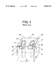
- FIG. 1 shows such a conventional dielectric filter comprising a dielectric block a which has an upper surface b where the ceramic material of the block is exposed and a front surface provided with an input and output terminals c.
- the dielectric block a is provided with a pair of resonance holes d which are extended between the upper surface b and the bottom surface thereof.
- On the upper surface b of the dielectric block a are provided a pair of recessed electrodes e extending from the respective input and output terminals c and a pair of jutted electrodes f extending from respective ends of the resonance holes d.
- each jutted electrode f is extended into the recessed portion of the corresponding recessed electrode e so that gaps g are formed between the jutted electrodes and the respective recessed electrodes to produce a desired input and a desired output coupling capacitance.
- a conventional dielectric filter having a configuration as described above is disadvantageous in that the jutted electrodes f and the recessed electrodes e have, by definition, a complicated profile having a number of lines such that the jutted portion of each of the electrodes f is received by the recessed potion of the corresponding electrode e. Therefore, it is practically impossible to regulate the capacitance of the filter once the jutted and recessed electrodes are formed and hence to achieve an optimum input and an optimum output coupling capacitance for the filter.
- a dielectric filter comprising a rectangular parallelepipedic dielectric ceramic block provided with at least a pair of resonance holes vertically bored therethrough, a conductive layer formed on the entire surface of the ceramic block except all or part of the top surface or the top and bottom surfaces of the block and a pair of input and output terminals arranged on a lateral side of the ceramic block, wherein trimming or capacitance regulating electrodes are provided on the top surface or on the top and bottom surfaces of the ceramic block, each extending from one of said input and output terminals to the vicinity of the opening of the corresponding resonance hole on the same side so that the input and output terminals and the resonance holes are capacitively coupled by way of the trimming electrodes.
- each of the trimming electrodes may comprise a single conductor member which is partly cut out or to which a compensating conductor is added for regulating the input and the output coupling capacitance of the filter.
- each of the trimming electrodes may comprise a plurality of small conductor pieces which are electrically bridged by a conductor paint for obtaining a predetermined input and a predetermined output coupling capacitance.
- FIG. 1 is a schematic perspective view of a conventional dielectric filter
- FIG. 2 is a schematic perspective view of a preferred embodiment of dielectric filter according to the present invention.
- FIG. 3 is a sectional view of the embodiment of FIG. 1 taken along I--I line;
- FIG. 4 is a sectional view of the embodiment of FIG. 1 taken along II--Il line;
- FIG. 5 is a partial perspective view of the embodiment of FIG. 1, showing one of the trimming electrodes partly eliminated at the front end thereof;
- FIG. 6 is a partial perspective view showing an alternative trimming electrode
- FIG. 7 is a schematic perspective view of another preferred embodiment of dielectric filter according to the present invention.
- FIGS. 2 through 5 that illustrate a first embodiment of the present invention, it comprises a rectangular parallelepipedic dielectric ceramic block 1 made of a dielectric ceramic composite having a high dielectric constant and a low loss rate such as BaO--TiO 2 or BaO--TiO 2 -rare earth element, through which a pair of resonance holes 2 are vertically bored to produce openings at the top surface 1a and the bottom surface 1b (see FIGS.
- a conductor layer 3 arranged on entire surface of the ceramic block 1 except the top surface 1a of the ceramic block 1, or on the four lateral side surfaces, the bottom surface 1b of the ceramic block 1 and the inner surfaces of the resonance holes 2, a pair of input and output terminals 4 arranged vis-a-vis the respective resonance holes 2 along the upper edge of a lateral side surface 1c (see FIGS. 2, 5) of the ceramic block 1, and a pair of trimming or capacitance regulating electrodes 5 (see FIGS. 2, 4 and 5) arranged on the top surface 1a of the ceramic block 1.
- the conductor layer 3 may be formed by depositing metal material having a high conductivity such as silver or copper on the surfaces of the dielectric ceramic block 1 except the top surface 1a of the dielectric ceramic block 1.
- Each of said trimming electrodes 5 has an end connected to the corresponding input or output terminal 4 and the other end extending to the vicinity of the corresponding resonance hole 2, so that the embodiment may have a desired input and a desired output coupling capacitance by securing appropriate gaps 6 (see FIGS. 2, 4 and 5) between the trimming electrodes 5 and the respective edges of the resonance holes 2.
- the input and the output coupling capacitance of a dielectric filter having a configuration as described above is a function of the size of the gaps 6 and the specific dielectric constant of the dielectric ceramic composite of the ceramic block 1, the dielectric filter, when manufactured, does not necessarily show a desired input and a desired output coupling capacitance because they are subject to errors that may take place during the manufacturing process.
- the capacitance across each of the gaps 6 is measured for the embodiment by using a capacitance gauge 7 which is connected between the corresponding one of the input and output terminals 4 and that of the resonance holes 2. If the capacitance exceeds a predetermined level, an appropriate front end portion 5' of the corresponding trimming electrode 5 is cut out by using a laser, a cutting tool or some other appropriate means to enlarge the gap 6. If, on the other hand, the capacitance falls short of the predetermined level, a small piece of conductor (not shown) is added to the front end of the trimming electrode 5 to reduce the gap 6.
- FIG. 6 is a partial perspective view of an alternative trimming electrode that can be used for the embodiment of FIG. 1 and is actually composed of a plurality of small pieces 5a, 5b, 5c, and 5d.
- the capacitance of the gap 6 separating the trimming electrode 5 and the corresponding resonance hole 2 is measured by means of the capacitance gauge 7 connected between the corresponding input or output terminal 4 and the resonance hole 2, and is regulated by applying a conductive paint 8 such as one made of pasty silver between, for instance, the pieces 5a and 5b to electrically connect them until a desired capacitance level is achieved.
- each of the resonance holes 2 is grounded by the conductor layer 3 (see FIGS. 3, 4) covering the bottom surface of the ceramic block 1 while the other end is electrically insulated by the exposed (dotted) top surface of the ceramic block 1 in the above embodiment.
- FIG. 7 illustrates another embodiment of the invention which is an interdigital type dielectric filter having three resonance holes 2, which are alternately grounded on the top surface 1a and the bottom surface 1b of the ceramic block 1 by way of respective conductor layers 3a, 3b and 3c connected to respective ends of the resonance holes, while the remaining ends of the resonance holes are electrically insulated by the respective exposed (dotted) areas of the top and the bottom surfaces of the ceramic block 1.
- a pair of trimming electrodes 5 are arranged so as to be connected to respective input and output terminals 4 and extended toward the respective outer resonance holes 2 and a desired coupling capacitance may be produced at each of the gaps 6 separating the input and output terminals 4 and the resonance holes 2 by appropriately trimming the trimming electrodes 5.
- the concept of the present invention can be applied not only to dielectric filters having a pair of resonance holes, as in the case of the first embodiment, but also to those having three or more resonance holes as shown in FIG. 7.
- each of the trimming electrodes may be connected at an end to the corresponding resonance hole and separated at the other end from an edge of the corresponding input or output terminal to produce a gap for coupling capacitance.
- the once established coupling capacitance may be varied when the dielectric filter is turned upside down on a printed circuit board and soldered to related circuits of the board as the gaps may be partly filled with solder.
- a dielectric filter according to the present invention and having a configuration as described above by way of embodiments is free from such a problem because the gaps are located close to the respective resonance holes and hence remote from the top surface of the printed circuit board if the filter is partly contaminated with solder.
- a dielectric filter according to the present invention is provided with trimming electrodes arranged respectively between its input and output terminals and resonance holes to regulate the coupling capacitance, a desired input and a desired output coupling capacitance can be easily achieved for the filter.
- high quality dielectric filters can be provided at low cost on an industrial basis.
Landscapes
- Physics & Mathematics (AREA)
- Electromagnetism (AREA)
- Control Of Motors That Do Not Use Commutators (AREA)
Applications Claiming Priority (2)
| Application Number | Priority Date | Filing Date | Title |
|---|---|---|---|
| JP044686U JPH0711002U (ja) | 1993-07-23 | 1993-07-23 | 誘電体フィルタ |
| JP5-044686U | 1993-07-23 |
Publications (1)
| Publication Number | Publication Date |
|---|---|
| US5818311A true US5818311A (en) | 1998-10-06 |
Family
ID=12698317
Family Applications (1)
| Application Number | Title | Priority Date | Filing Date |
|---|---|---|---|
| US08/277,277 Expired - Fee Related US5818311A (en) | 1993-07-23 | 1994-07-21 | Dielectric filter including trimming electrodes |
Country Status (5)
| Country | Link |
|---|---|
| US (1) | US5818311A (ko) |
| EP (1) | EP0635897B1 (ko) |
| JP (1) | JPH0711002U (ko) |
| KR (1) | KR0177189B1 (ko) |
| DE (1) | DE69420911T2 (ko) |
Cited By (1)
| Publication number | Priority date | Publication date | Assignee | Title |
|---|---|---|---|---|
| US20030042996A1 (en) * | 2001-09-06 | 2003-03-06 | Shoji Ono | Dielectric duplexer |
Families Citing this family (7)
| Publication number | Priority date | Publication date | Assignee | Title |
|---|---|---|---|---|
| US5841332A (en) * | 1995-11-16 | 1998-11-24 | Ngk Spark Plug Co., Ltd. | Dielectric filter and method of adjusting central frequency of the same |
| JPH1022710A (ja) * | 1996-07-03 | 1998-01-23 | Ngk Spark Plug Co Ltd | 誘電体フィルタの電極形成方法 |
| US6081174A (en) * | 1997-03-14 | 2000-06-27 | Taiyo Yuden Co., Ltd. | Wave filter having two or more coaxial dielectric resonators in juxtaposition |
| KR100299052B1 (ko) * | 1998-08-21 | 2001-10-27 | 오길록 | 무선통신시스템용대역통과필터 |
| DE60032300T2 (de) | 1999-09-24 | 2007-06-28 | NGK Spark Plug Co., Ltd., Nagoya | Dielektrisches Filter und dessen Herstellungsverfahren |
| KR101504957B1 (ko) * | 2013-08-13 | 2015-03-23 | 한국광성전자 주식회사 | 세라믹 모노 블록 및 이를 이용한 세라믹 필터의 입출력단자 및 상면 패턴 형성 방법 |
| KR20220037225A (ko) * | 2020-09-17 | 2022-03-24 | 주식회사 엘지에너지솔루션 | 우수한 방열 성능을 구비한 버스바 |
Citations (9)
| Publication number | Priority date | Publication date | Assignee | Title |
|---|---|---|---|---|
| US4462098A (en) * | 1982-02-16 | 1984-07-24 | Motorola, Inc. | Radio frequency signal combining/sorting apparatus |
| JPS6052102A (ja) * | 1983-09-01 | 1985-03-25 | Oki Electric Ind Co Ltd | 誘電体共振器および誘電体共振器の共振周波数の調整方法 |
| JPS6238601A (ja) * | 1985-08-13 | 1987-02-19 | Murata Mfg Co Ltd | インタ−デジタル型フイルタおよびその製造方法 |
| US4673902A (en) * | 1983-11-25 | 1987-06-16 | Murata Manufacturing Co., Ltd. | Dielectric material coaxial resonator filter directly mountable on a circuit board |
| US4675632A (en) * | 1984-02-23 | 1987-06-23 | Mitsubishi Denki Kabushiki Kaisha | Coaxial line shape resonator with high dielectric constant |
| US4800348A (en) * | 1987-08-03 | 1989-01-24 | Motorola, Inc. | Adjustable electronic filter and method of tuning same |
| US5198788A (en) * | 1991-11-01 | 1993-03-30 | Motorola, Inc. | Laser tuning of ceramic bandpass filter |
| JPH06164205A (ja) * | 1992-11-17 | 1994-06-10 | Oki Electric Ind Co Ltd | 誘電体フィルタ |
| US5327108A (en) * | 1991-03-12 | 1994-07-05 | Motorola, Inc. | Surface mountable interdigital block filter having zero(s) in transfer function |
Family Cites Families (7)
| Publication number | Priority date | Publication date | Assignee | Title |
|---|---|---|---|---|
| JPS5773501A (en) * | 1980-10-25 | 1982-05-08 | Fujitsu Ltd | Dielectric filter element and dielectric filter |
| JPS63110801A (ja) * | 1986-10-28 | 1988-05-16 | Murata Mfg Co Ltd | アクテイブフイルタ |
| JPH0642602B2 (ja) * | 1987-09-10 | 1994-06-01 | 三菱電機株式会社 | 誘電体フィルタ |
| JPH02241203A (ja) * | 1989-03-15 | 1990-09-25 | Matsushita Electric Ind Co Ltd | 同軸共振器およびそれを用いたフィルタ |
| JPH04150101A (ja) * | 1990-10-08 | 1992-05-22 | Murata Mfg Co Ltd | 誘電体共振器 |
| US5208566A (en) * | 1992-01-21 | 1993-05-04 | Motorola, Inc. | Dielectric filter having adjacently-positioned resonators of dissimilar cross-sectional dimensions and notched side surface |
| DE69325525T2 (de) * | 1992-01-23 | 1999-12-23 | Murata Mfg. Co., Ltd. | Dielektrisches Filter und Herstellungsverfahren dafür |
-
1993
- 1993-07-23 JP JP044686U patent/JPH0711002U/ja active Pending
-
1994
- 1994-07-21 KR KR1019940017604A patent/KR0177189B1/ko not_active IP Right Cessation
- 1994-07-21 US US08/277,277 patent/US5818311A/en not_active Expired - Fee Related
- 1994-07-22 EP EP94305424A patent/EP0635897B1/en not_active Expired - Lifetime
- 1994-07-22 DE DE69420911T patent/DE69420911T2/de not_active Expired - Fee Related
Patent Citations (9)
| Publication number | Priority date | Publication date | Assignee | Title |
|---|---|---|---|---|
| US4462098A (en) * | 1982-02-16 | 1984-07-24 | Motorola, Inc. | Radio frequency signal combining/sorting apparatus |
| JPS6052102A (ja) * | 1983-09-01 | 1985-03-25 | Oki Electric Ind Co Ltd | 誘電体共振器および誘電体共振器の共振周波数の調整方法 |
| US4673902A (en) * | 1983-11-25 | 1987-06-16 | Murata Manufacturing Co., Ltd. | Dielectric material coaxial resonator filter directly mountable on a circuit board |
| US4675632A (en) * | 1984-02-23 | 1987-06-23 | Mitsubishi Denki Kabushiki Kaisha | Coaxial line shape resonator with high dielectric constant |
| JPS6238601A (ja) * | 1985-08-13 | 1987-02-19 | Murata Mfg Co Ltd | インタ−デジタル型フイルタおよびその製造方法 |
| US4800348A (en) * | 1987-08-03 | 1989-01-24 | Motorola, Inc. | Adjustable electronic filter and method of tuning same |
| US5327108A (en) * | 1991-03-12 | 1994-07-05 | Motorola, Inc. | Surface mountable interdigital block filter having zero(s) in transfer function |
| US5198788A (en) * | 1991-11-01 | 1993-03-30 | Motorola, Inc. | Laser tuning of ceramic bandpass filter |
| JPH06164205A (ja) * | 1992-11-17 | 1994-06-10 | Oki Electric Ind Co Ltd | 誘電体フィルタ |
Cited By (2)
| Publication number | Priority date | Publication date | Assignee | Title |
|---|---|---|---|---|
| US20030042996A1 (en) * | 2001-09-06 | 2003-03-06 | Shoji Ono | Dielectric duplexer |
| US6798316B2 (en) * | 2001-09-06 | 2004-09-28 | Ngk Spark Plug.Co., Ltd. | Dielectric duplexer |
Also Published As
| Publication number | Publication date |
|---|---|
| KR950004628A (ko) | 1995-02-18 |
| JPH0711002U (ja) | 1995-02-14 |
| KR0177189B1 (ko) | 1999-05-15 |
| EP0635897B1 (en) | 1999-09-29 |
| DE69420911D1 (de) | 1999-11-04 |
| DE69420911T2 (de) | 2000-02-03 |
| EP0635897A1 (en) | 1995-01-25 |
Similar Documents
| Publication | Publication Date | Title |
|---|---|---|
| US6046409A (en) | Multilayer microelectronic circuit | |
| US4673902A (en) | Dielectric material coaxial resonator filter directly mountable on a circuit board | |
| US5349314A (en) | Stripline filter device having a coupling dielectric layer between two stripline resonators | |
| US4975664A (en) | Filter device | |
| JPH07283604A (ja) | 誘電体フィルタ装置 | |
| US5187455A (en) | Delay line device with adjustable time delay | |
| US5818311A (en) | Dielectric filter including trimming electrodes | |
| US5825262A (en) | Ladder filter with piezoelectric resonators each having a plurality of layers with internal electrodes | |
| US6160462A (en) | Energy trapping type piezoelectric filter with identical piezoelectric substrates | |
| US5475350A (en) | Frequency tunable resonator including a varactor | |
| EP0746052B1 (en) | Dielectric filter | |
| US5831497A (en) | Dielectirc resonator apparatus | |
| GB2256973A (en) | Method of adjusting a frequency response in a microwave strip-line filter device. | |
| US6924707B2 (en) | Resonator | |
| EP0568370B1 (en) | Dielectric filter device | |
| US5563560A (en) | Coupling capacitance dielectric board for coaxial resonators | |
| JPH11340709A (ja) | 回路基板およびそれを用いた電子装置 | |
| US6392505B1 (en) | Dielectric device | |
| US6034579A (en) | Dielectric filter of the band elimination type | |
| JPH05167310A (ja) | 誘電体フィルタおよび共振器 | |
| US5936491A (en) | Dielectric filter | |
| JPH0613802A (ja) | 同軸共振器及びこれを用いた誘電体フィルタ | |
| JP3159025B2 (ja) | 誘電体フィルタ | |
| JPH0794921A (ja) | 誘電体同軸共振器 | |
| JPH07161582A (ja) | チップ形コンデンサネットワーク部品 |
Legal Events
| Date | Code | Title | Description |
|---|---|---|---|
| AS | Assignment |
Owner name: NGK SPARK PLUG CO., LTD., JAPAN Free format text: ASSIGNMENT OF ASSIGNORS INTEREST;ASSIGNOR:HINO, SEIGO;REEL/FRAME:007076/0022 Effective date: 19940607 |
|
| FEPP | Fee payment procedure |
Free format text: PAYOR NUMBER ASSIGNED (ORIGINAL EVENT CODE: ASPN); ENTITY STATUS OF PATENT OWNER: LARGE ENTITY |
|
| FEPP | Fee payment procedure |
Free format text: PAYER NUMBER DE-ASSIGNED (ORIGINAL EVENT CODE: RMPN); ENTITY STATUS OF PATENT OWNER: LARGE ENTITY |
|
| FEPP | Fee payment procedure |
Free format text: PAYOR NUMBER ASSIGNED (ORIGINAL EVENT CODE: ASPN); ENTITY STATUS OF PATENT OWNER: LARGE ENTITY |
|
| FPAY | Fee payment |
Year of fee payment: 4 |
|
| FPAY | Fee payment |
Year of fee payment: 8 |
|
| REMI | Maintenance fee reminder mailed | ||
| LAPS | Lapse for failure to pay maintenance fees | ||
| STCH | Information on status: patent discontinuation |
Free format text: PATENT EXPIRED DUE TO NONPAYMENT OF MAINTENANCE FEES UNDER 37 CFR 1.362 |
|
| FP | Lapsed due to failure to pay maintenance fee |
Effective date: 20101006 |