US5006738A - Delay circuit for integrated circuit - Google Patents
Delay circuit for integrated circuit Download PDFInfo
- Publication number
- US5006738A US5006738A US07/537,868 US53786890A US5006738A US 5006738 A US5006738 A US 5006738A US 53786890 A US53786890 A US 53786890A US 5006738 A US5006738 A US 5006738A
- Authority
- US
- United States
- Prior art keywords
- delay circuit
- transistors
- transistor
- capacitance
- mis transistors
- Prior art date
- Legal status (The legal status is an assumption and is not a legal conclusion. Google has not performed a legal analysis and makes no representation as to the accuracy of the status listed.)
- Expired - Lifetime
Links
Images

Classifications
-
- H—ELECTRICITY
- H03—ELECTRONIC CIRCUITRY
- H03H—IMPEDANCE NETWORKS, e.g. RESONANT CIRCUITS; RESONATORS
- H03H11/00—Networks using active elements
- H03H11/02—Multiple-port networks
- H03H11/26—Time-delay networks
-
- G—PHYSICS
- G11—INFORMATION STORAGE
- G11C—STATIC STORES
- G11C19/00—Digital stores in which the information is moved stepwise, e.g. shift registers
- G11C19/18—Digital stores in which the information is moved stepwise, e.g. shift registers using capacitors as main elements of the stages
- G11C19/182—Digital stores in which the information is moved stepwise, e.g. shift registers using capacitors as main elements of the stages in combination with semiconductor elements, e.g. bipolar transistors, diodes
- G11C19/184—Digital stores in which the information is moved stepwise, e.g. shift registers using capacitors as main elements of the stages in combination with semiconductor elements, e.g. bipolar transistors, diodes with field-effect transistors, e.g. MOS-FET
-
- H—ELECTRICITY
- H03—ELECTRONIC CIRCUITRY
- H03K—PULSE TECHNIQUE
- H03K5/00—Manipulating of pulses not covered by one of the other main groups of this subclass
- H03K5/13—Arrangements having a single output and transforming input signals into pulses delivered at desired time intervals
- H03K5/133—Arrangements having a single output and transforming input signals into pulses delivered at desired time intervals using a chain of active delay devices
-
- H—ELECTRICITY
- H03—ELECTRONIC CIRCUITRY
- H03K—PULSE TECHNIQUE
- H03K5/00—Manipulating of pulses not covered by one of the other main groups of this subclass
- H03K2005/00013—Delay, i.e. output pulse is delayed after input pulse and pulse length of output pulse is dependent on pulse length of input pulse
- H03K2005/0015—Layout of the delay element
- H03K2005/00195—Layout of the delay element using FET's
Definitions
- This invention relates to a delay circuit for producing a certain delay time and more particularly to an improved a delay circuit for integrated circuits, such as CMOS circuits.
- data signals are latched at the outputs thereof after the address signals are applied, and then the memory cells are in the stand-by state to reduce the power consumption (PWL system; pulsed word line system).
- PWL system pulsed word line system
- a delay circuit is used since a waiting time of one cycle is needed.
- FIGS. 4 and 5 show an example of the prior art delay circuit for use in such memory devices.
- FIG. 4 shows the basic construction of the conventional delay circuit wherein a capacitance 42, such as a MOS capacitor, is connected to the output side of an inverter circuit 41.
- FIG. 5 shows a circuit for obtaining a longer delay time.
- the circuit has a plurality of inverter circuits 51 through 54 with capacitors 55 through 58 provided following each of the inverter circuits.
- the input/output inverting operation is performed when the threshold voltage of each inverter is exceeded so that the capacitors 55-58 are charged gradually.
- the similar operation takes place when the voltage value at the capacitors 55-58 exceeds the threshold voltage of the next stage inverter circuit.
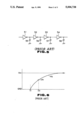
- FIG. 6 is a waveform diagram showing output signals of the conventional delay circuits employing one or more inverter circuits.
- the inverter circuit is formed by a CMOS inverter
- a waveform PA is obtained.
- the waveform PA starts to rise at the time ⁇ 1 and exceeds the threshold voltage Vth of the next stage at time ⁇ 2 .
- ⁇ 2 the waveform PA presents a curve that is upwardly convex due to the drive capability of the PMOS transistor in the inverter such that the voltage PA approaches the source voltage Vcc gradually.
- the above delay circuit is subject to performance differences due to manufacturing variations. For example, when the channel length of the transistor making up the inverter circuit varies, the threshold voltage Vth is changed, with a resulting increase or decrease in the delay time. When a longer delay time is desired, the number of stages is increased correspondingly. The result is that the space required for the additional circuitry is increased in an amount corresponding to the increased number of the circuits, such as the inverter circuits.
- the delay time is set by the time between ⁇ 1 and ⁇ 2 ( ⁇ 2 - ⁇ 1 ) in FIG. 6 as the reference.
- the waveform PA rises exponentially so that it is difficult to set the exact delay time.
- the performance differences of the circuits making up the multiple stage embodiment are added to one another to make the delay time is even less exact.
- an improved delay circuit for integrated circuits is provided in a complementary MIS (metal-insulated-semiconductor) structure.
- the delay circuit includes a pair of current mirror connected MIS transistors, a constant current source and a capacitance.
- the constant current source is connected to one of the MIS transistors in order to determine the current through the MIS transistor.
- the capacitance is connected to the other of the MIS transistors which serves as a current path.
- the delay time is determined by the charging time of the capacitance.
- the quantity of current provided to charge the capacitance is dependent on the ratio of the current capability or Q factor of the pair of the MIS transistors.
- FIG. 1 is a circuit diagram showing an example of the delay circuit of the present invention
- FIG. 2 is a waveform diagram showing the output signals
- FIG. 3 is a circuit diagram showing another example of the delay circuit of the present invention.
- FIG. 4 is a circuit diagram showing an example of the conventional delay circuit
- FIG. 5 is a circuit diagram showing another example of a conventional delay circuit.
- FIG. 6 is a wave form diagram showing output signals of the conventional delay circuit.
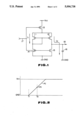
- the first embodiment has a circuit construction of the present invention is shown in FIG. 1.
- a pair of PMOS transistors (p-channel MOSFETs) 11, 12 are connected in a gate common configuration so as to constitute a current mirror circuit.
- the common connected gate is connected to the drain side of the PMOS transistor 11.
- the respective sources of the pair of PMOS transistors 11, 12 are connected to a PMOS transistor 13 connected in common and acting as a switch.
- the transistor 13 has its source connected to a source voltage Vcc.
- a PMOS transistor 14 as a constant current source is connected to a drain of the PMOS transistor 11.
- the PMOS transistor 14 has its drain connected to ground GND and input signals are supplied to the gate via input 17.
- the PMOS transistor 12 has its drain connected to a capacitor 16 for storing the electrical charges and a NMOS transistor (n-channel MOSFET) 15 for controlling the charging and discharging of the capacitor 16.
- the NMOS transistor 15 has its gate connected in common with the gate of the PMOS transistor 14 to the input 17.
- the NMOS transistor 15 has its source connected to a ground voltage GND.
- the electrode of the capacitor 16 connected to the drain of the PMOS transistor 12 is connected to the output 18.
- the other electrode of the capacitor 16 is connected to a ground voltage GND.
- the PMOS transistor 13 may be dispensed with.
- the capacitor 16 may also be a gate capacitance of a MOS transistor.
- the delay circuit of the first embodiment having the above circuit construction operates in the following manner.
- the input signal is set to "H” (high) level at first.
- the PMOS transistors 13, 14 are both turned off.
- the NMOS transistor 15 is simultaneously turned on.
- the capacitor 16 has its both ends connected to the ground voltage GND and is reset. Therefore, the output signal of the delay circuit is at "L" (low) level.
- the input signal is then changed from the "H” to the "L” level. This causes the NMOS transistor 15 to be turned off and both the PMOS transistors 13, 14 to be turned on. With the PMOS transistors 13, 14 both turned on, current I 1 flows in the transistors 13, 11, and 14.
- This current I 1 is determined by the PMOS transistor 14 as the constant current source and more specifically the size of the PMOS transistor 14, threshold voltage Vth, etc.
- the current I 1 flowing in the PMOS transistor 11 also determines the current I 2 of the PMOS transistor 12 since the PMOS transistors 11 and 12 are connected is a current mirror configuration.
- the value of the current I 2 is given by the formula;
- the current I 2 flowing in the PMOS transistor 12 having its value determined by the PMOS transistors 11, 13 flows into the capacitor 16, since the NMOS transistor 15 is turned off.
- the current I 2 charging capacity 16 has a constant current value and gives a constant charging time.
- FIG. 2 shows the voltage rise in the capacitor 16 caused by the current I 2 , that is, the waveform PI of the output signals.
- the waveform PI rises substantially linearly from time T 1 , and exceeds the next stage threshold voltage Vth at time T 2 .
- the next stage threshold voltage Vth is exceeded, delayed output signals of the delay circuit with respect to the input signals are obtained.
- Plural similar delay circuit stages may be provided following the circuit of FIG. 1 as the next stage and a waveform shaping circuit may also be provided.
- the delay circuit of the first embodiment in order that the PMOS transistor 14 operates ideally as the constant current source, it suffices that the current capability Q 1 of the PMOS transistor 11 be sufficiently larger than the current capability of Q 3 of the PMOS transistor 14. For obtaining a long delay time, it is necessary that a small current I 2 flows in the PMOS transistor 12, so that the current capability of the PMOS transistor 11 should be sufficiently larger than that of the PMOS transistor 12.
- These current capabilities Q 1 , to Q 3 are determined by manufacturing parameters (such as channel lengths and widths, concentration of impurities, etc.). These parameters, if changed for manufacturing reasons, are changed uniformly. Therefore, the ratio of the current capabilities is not affected by manufacturing fluctuations. Therefore, the delay circuit is relatively immune to manufacturing fluctuations. For example, the fluctuations of the current I 1 are suppressed by increasing the channel length of the PMOS transistor 14. Since the relation of the PMOS transistors 11 and 12 is kept constant, the delay time of the delay circuit of the first embodiment is not affected by fluctuations in the channel length.
- the output signals are changed substantially linearly, so that the delay time can be set easily. That is, the time difference between the time T 2 and time T 1 can be set with less error as compared with the exponential type circuit (see FIG. 6).
- a stable and readily determinable delay time can be achieved.
- Longer delay time can also be obtained by increasing the capacitance of the capacitor 16.
- a longer delay time can be obtained easily by setting the ratio between the current capabilities Q 1 and Q 2 so as to be larger. Hence, an extremely small capacitor 16 suffices and the space occupied by the circuit can be reduced.
- the constant current source is constituted by a NMOS transistor to elevate the NMOS transistor dependency of the circuit.
- the delay circuit of the second embodiment has the structure as shown in FIG. 3. Similar to the delay circuit of the first embodiment, a pair of PMOS transistors 21 and 22 are connected in a gate common configuration to form a current mirror circuit. The common connected gates are connected to the drain side of the PMOS transistor 21.
- the paired PMOS transistors 21 and 22 have the sources connected in common and connected to a PMOS transistor 23 acting as a switch.
- the PMOS transistor 23 has its source connected to a source voltage Vcc.
- a NMOS transistor 24 as a constant current source is connected to a drain of the PMOS transistor 21.
- the NMOS transistor 24 has its source connected to a ground voltage GND and the input signals are supplied from the input 27 via an inverter circuit 29.
- a NMOS transistor 25 for controlling the charging and discharging of the capacitor 26 is connected to the drain of the PMOS transistor 22. To the gate of the NMOS transistor 25 are applied input signals from the input 27. The source of the NMOS transistor 25 is connected to the ground voltage GND. The electrode of the capacitor 26 connected to the drain side of the PMOS transistor 22 is connected to an output 28 supplying output signals. The other electrode of the capacitor 26 is connected to the ground voltage GND.
- the PMOS transistor 23 may be dispensed with.
- the capacitor 26 may be the gate capacitance etc. of the MOS transistor.
- the operation of the delay circuit of the second embodiment having the above circuit configuration is substantially the same as that of the delay circuit of the first embodiment, the only difference being that the NMOS transistor 24 is used as the PMOS transistor 14 of the constant current source.
- the NMOS transistor 25 is turned from the ON state to the OFF state, for releasing the reset state of the capacity 26.
- the NMOS transistor 24 is turned to the ON state from the OFF state.
- the current value I 1 ' of the PMOS transistor 21 can be determined by rendering the current capability Q 3 ' of the NMOS transistor 24 substantially less than the current capability Q 1 ' of the PMOS transistor 21.
- the relation of the equation (1) in the first embodiment holds true between the current mirror connected PMOS transistor 21 and 22. Therefore, the amount of the current flowing into the capacitor 26 is determined by the NMOS transistor 24.
- NMOS transistor dependency of the circuit may be provided by using the NMOS transistor 24 as the constant current source.
- the NMOS transistor element is slightly faster than the design value, the tendency is reflected on the delay circuit.
- the manufacturing parameters, if changed, are changed uniformly for the delay circuit of the second embodiment, so that the ratio of the current capabilities is not affected by the manufacturing fluctuations.
- the output as shown in FIG. 2 is obtained in the delay circuit of the second embodiment and the transition is substantially linear so that error is minimized and a stable delay time may be obtained.
- the desired long delay time can be obtained by selecting the capacitance of the capacitor 26 to be larger, however, a longer delay time can be obtained easily by reducing the current value I 1 ' based on the constant current source or selecting the ratio of the current capabilities of the pair of PMOS transistors 21 and 22 connected in the current mirror configuration. In this manner, the occupation space required by the capacitor 26 can be reduced substantially.
- plural delay circuits according to the invention may be connected together to form a delay circuit.
Landscapes
- Engineering & Computer Science (AREA)
- Microelectronics & Electronic Packaging (AREA)
- Power Engineering (AREA)
- Physics & Mathematics (AREA)
- Nonlinear Science (AREA)
- Pulse Circuits (AREA)
Applications Claiming Priority (2)
| Application Number | Priority Date | Filing Date | Title |
|---|---|---|---|
| JP62-276874 | 1987-10-31 | ||
| JP62276874A JPH01119114A (ja) | 1987-10-31 | 1987-10-31 | ディレイ回路 |
Related Parent Applications (1)
| Application Number | Title | Priority Date | Filing Date |
|---|---|---|---|
| US07263389 Continuation | 1988-10-27 |
Publications (1)
| Publication Number | Publication Date |
|---|---|
| US5006738A true US5006738A (en) | 1991-04-09 |
Family
ID=17575608
Family Applications (1)
| Application Number | Title | Priority Date | Filing Date |
|---|---|---|---|
| US07/537,868 Expired - Lifetime US5006738A (en) | 1987-10-31 | 1990-06-13 | Delay circuit for integrated circuit |
Country Status (4)
| Country | Link |
|---|---|
| US (1) | US5006738A (ja) |
| EP (1) | EP0315385B1 (ja) |
| JP (1) | JPH01119114A (ja) |
| DE (1) | DE3889069T2 (ja) |
Cited By (17)
| Publication number | Priority date | Publication date | Assignee | Title |
|---|---|---|---|---|
| US5175454A (en) * | 1991-02-22 | 1992-12-29 | Sony Corporation | Programmable delay circuit having n-stage capacitance elements |
| US5369310A (en) * | 1992-06-01 | 1994-11-29 | Hewlett-Packard Corporation | CMOS power-on reset circuit |
| US5382840A (en) * | 1991-09-30 | 1995-01-17 | Siemens Aktiengesellschaft | Analog delay circuit configuration |
| US5696440A (en) * | 1993-09-30 | 1997-12-09 | Nec Corporation | Constant current generating apparatus capable of stable operation |
| US5900771A (en) * | 1996-12-12 | 1999-05-04 | Nat Semiconductor Corp | Capacitive multiplier for timing generation |
| US5936451A (en) * | 1994-12-29 | 1999-08-10 | Stmicroeletronics, Inc. | Delay circuit and method |
| US6388491B1 (en) * | 1998-04-28 | 2002-05-14 | Seiko Instruments Inc. | Delay circuit |
| DE10056881A1 (de) * | 2000-11-16 | 2002-05-29 | Infineon Technologies Ag | Integrierter Speicher |
| US6480050B1 (en) * | 1999-09-09 | 2002-11-12 | Stmicroelectronics Limited | Level shifter with no quiescent DC current flow |
| US20030021154A1 (en) * | 2001-02-22 | 2003-01-30 | Yeong-Taek Lee | Bit line setup and discharge circuit for programming non-volatile memory |
| US7042266B2 (en) * | 2000-08-10 | 2006-05-09 | Nec Electronics Corporation | Delay circuit and method |
| US20060135350A1 (en) * | 2004-12-17 | 2006-06-22 | Fina Technology, Inc. | Diketonate complex-derived catalysts useful for preparing polyolefins |
| DE10317279B4 (de) * | 2002-04-12 | 2006-09-28 | Samsung Electronics Co., Ltd., Suwon | Verzögerungsschaltung |
| US20070128388A1 (en) * | 2005-12-02 | 2007-06-07 | Fina Technology, Inc. | Polymer compositions for reduced shrinkage |
| USRE42250E1 (en) | 1994-12-29 | 2011-03-29 | Stmicroelectronics, Inc. | Delay circuit and method |
| US8466729B2 (en) | 2011-08-11 | 2013-06-18 | National Chiao Tung University | Delay cell and digitally controlled oscillator |
| CN105281727A (zh) * | 2014-07-24 | 2016-01-27 | 登丰微电子股份有限公司 | 延时电路 |
Families Citing this family (6)
| Publication number | Priority date | Publication date | Assignee | Title |
|---|---|---|---|---|
| JPH0812986B2 (ja) * | 1989-06-20 | 1996-02-07 | 日本電気株式会社 | 遅延回路 |
| FR2671244B1 (fr) * | 1990-12-27 | 1993-03-05 | Bull Sa | Dispositif de retard reglable. |
| FR2671245B1 (fr) * | 1990-12-27 | 1993-03-05 | Bull Sa | Dispositif de retard reglable. |
| EP0608666B1 (en) * | 1993-01-29 | 1998-04-29 | STMicroelectronics S.r.l. | Time delay filter monolithically integratable |
| JP5242262B2 (ja) * | 2008-07-03 | 2013-07-24 | ルネサスエレクトロニクス株式会社 | 移相回路、装置及び方法 |
| JP5967362B2 (ja) * | 2012-06-29 | 2016-08-10 | セイコーNpc株式会社 | 遅延回路 |
Citations (9)
| Publication number | Priority date | Publication date | Assignee | Title |
|---|---|---|---|---|
| UST926003I4 (en) * | 1972-08-25 | 1974-09-03 | Polyphase logical circuit employing complementary misfet | |
| US3895239A (en) * | 1973-12-26 | 1975-07-15 | Motorola Inc | MOS power-on reset circuit |
| US3937982A (en) * | 1973-03-20 | 1976-02-10 | Nippon Electric Co., Inc. | Gate circuit |
| US4424456A (en) * | 1979-12-26 | 1984-01-03 | Tokyo Shibaura Denki Kabushiki Kaisha | Driver circuit for charge coupled device |
| US4499387A (en) * | 1981-12-15 | 1985-02-12 | Tokyo Shibaura Denki Kabushiki Kaisha | Integrated circuit formed on a semiconductor substrate with a variable capacitor circuit |
| US4644182A (en) * | 1984-11-13 | 1987-02-17 | Fujitsu Limited | Delay circuit having delay time period determined by discharging operation |
| US4752703A (en) * | 1987-04-23 | 1988-06-21 | Industrial Technology Research Institute | Current source polarity switching circuit |
| US4812687A (en) * | 1988-07-13 | 1989-03-14 | International Business Machines Corporation | Dual direction integrating delay circuit |
| US4835489A (en) * | 1987-02-13 | 1989-05-30 | National Semiconductor Corporation | Single-ended, feed-forward gain stage |
Family Cites Families (3)
| Publication number | Priority date | Publication date | Assignee | Title |
|---|---|---|---|---|
| DE2553517C3 (de) * | 1975-11-28 | 1978-12-07 | Ibm Deutschland Gmbh, 7000 Stuttgart | Verzögerungsschaltung mit Feldeffekttransistoren |
| US4302691A (en) * | 1979-12-12 | 1981-11-24 | Sprague Electric Company | Integrated delay circuit with PN-junction capacitor |
| DE3676297D1 (de) * | 1986-03-12 | 1991-01-31 | Itt Ind Gmbh Deutsche | Integrierte isolierschicht-feldeffekttransistor-verzoegerungsleitung fuer digitalsignale. |
-
1987
- 1987-10-31 JP JP62276874A patent/JPH01119114A/ja active Pending
-
1988
- 1988-10-28 DE DE3889069T patent/DE3889069T2/de not_active Expired - Fee Related
- 1988-10-28 EP EP88310186A patent/EP0315385B1/en not_active Expired - Lifetime
-
1990
- 1990-06-13 US US07/537,868 patent/US5006738A/en not_active Expired - Lifetime
Patent Citations (9)
| Publication number | Priority date | Publication date | Assignee | Title |
|---|---|---|---|---|
| UST926003I4 (en) * | 1972-08-25 | 1974-09-03 | Polyphase logical circuit employing complementary misfet | |
| US3937982A (en) * | 1973-03-20 | 1976-02-10 | Nippon Electric Co., Inc. | Gate circuit |
| US3895239A (en) * | 1973-12-26 | 1975-07-15 | Motorola Inc | MOS power-on reset circuit |
| US4424456A (en) * | 1979-12-26 | 1984-01-03 | Tokyo Shibaura Denki Kabushiki Kaisha | Driver circuit for charge coupled device |
| US4499387A (en) * | 1981-12-15 | 1985-02-12 | Tokyo Shibaura Denki Kabushiki Kaisha | Integrated circuit formed on a semiconductor substrate with a variable capacitor circuit |
| US4644182A (en) * | 1984-11-13 | 1987-02-17 | Fujitsu Limited | Delay circuit having delay time period determined by discharging operation |
| US4835489A (en) * | 1987-02-13 | 1989-05-30 | National Semiconductor Corporation | Single-ended, feed-forward gain stage |
| US4752703A (en) * | 1987-04-23 | 1988-06-21 | Industrial Technology Research Institute | Current source polarity switching circuit |
| US4812687A (en) * | 1988-07-13 | 1989-03-14 | International Business Machines Corporation | Dual direction integrating delay circuit |
Non-Patent Citations (6)
| Title |
|---|
| "Electronics Engineers' Handbook"; editor; Fink, Donald; McGraw-Hill Book Company, Second Edition, pp. (16-16)-(16-19). |
| Electronics Engineers Handbook ; editor; Fink, Donald; McGraw Hill Book Company, Second Edition, pp. (16 16) (16 19). * |
| IBM Tech. Disc. Bult., Hanafi, Delay Driver Circuit, Jan. 81, p. 3610. * |
| IBM Tech. Disc. Bult., Hanafi, Delay Driver Circuit, Jan. '81, p. 3610. |
| IBM Tech. Disc. Bult., Sonoda, MOSFET Powering Circuit, Feb. 71, p. 2658. * |
| IBM Tech. Disc. Bult., Sonoda, MOSFET Powering Circuit, Feb. '71, p. 2658. |
Cited By (22)
| Publication number | Priority date | Publication date | Assignee | Title |
|---|---|---|---|---|
| US5175454A (en) * | 1991-02-22 | 1992-12-29 | Sony Corporation | Programmable delay circuit having n-stage capacitance elements |
| US5382840A (en) * | 1991-09-30 | 1995-01-17 | Siemens Aktiengesellschaft | Analog delay circuit configuration |
| US5369310A (en) * | 1992-06-01 | 1994-11-29 | Hewlett-Packard Corporation | CMOS power-on reset circuit |
| US5696440A (en) * | 1993-09-30 | 1997-12-09 | Nec Corporation | Constant current generating apparatus capable of stable operation |
| US5936451A (en) * | 1994-12-29 | 1999-08-10 | Stmicroeletronics, Inc. | Delay circuit and method |
| USRE42250E1 (en) | 1994-12-29 | 2011-03-29 | Stmicroelectronics, Inc. | Delay circuit and method |
| US5900771A (en) * | 1996-12-12 | 1999-05-04 | Nat Semiconductor Corp | Capacitive multiplier for timing generation |
| US6388491B1 (en) * | 1998-04-28 | 2002-05-14 | Seiko Instruments Inc. | Delay circuit |
| US6480050B1 (en) * | 1999-09-09 | 2002-11-12 | Stmicroelectronics Limited | Level shifter with no quiescent DC current flow |
| US7042266B2 (en) * | 2000-08-10 | 2006-05-09 | Nec Electronics Corporation | Delay circuit and method |
| DE10056881A1 (de) * | 2000-11-16 | 2002-05-29 | Infineon Technologies Ag | Integrierter Speicher |
| US20030021154A1 (en) * | 2001-02-22 | 2003-01-30 | Yeong-Taek Lee | Bit line setup and discharge circuit for programming non-volatile memory |
| US7453729B2 (en) | 2001-02-22 | 2008-11-18 | Samsung Electronics Co., Ltd. | Bit line setup and discharge circuit for programming non-volatile memory |
| US20090073775A1 (en) * | 2001-02-22 | 2009-03-19 | Yeong-Taek Lee | Bit line setup and discharge circuit for programming non-volatile memory |
| US7835191B2 (en) | 2001-02-22 | 2010-11-16 | Samsung Electronics Co., Ltd. | Bit line setup and discharge circuit for programming non-volatile memory |
| DE10317279B4 (de) * | 2002-04-12 | 2006-09-28 | Samsung Electronics Co., Ltd., Suwon | Verzögerungsschaltung |
| CN1452176B (zh) * | 2002-04-12 | 2012-05-23 | 三星电子株式会社 | 半导体存储器延迟电路 |
| US20060135350A1 (en) * | 2004-12-17 | 2006-06-22 | Fina Technology, Inc. | Diketonate complex-derived catalysts useful for preparing polyolefins |
| US20070128388A1 (en) * | 2005-12-02 | 2007-06-07 | Fina Technology, Inc. | Polymer compositions for reduced shrinkage |
| US8466729B2 (en) | 2011-08-11 | 2013-06-18 | National Chiao Tung University | Delay cell and digitally controlled oscillator |
| CN105281727A (zh) * | 2014-07-24 | 2016-01-27 | 登丰微电子股份有限公司 | 延时电路 |
| CN105281727B (zh) * | 2014-07-24 | 2018-06-01 | 登丰微电子股份有限公司 | 延时电路 |
Also Published As
| Publication number | Publication date |
|---|---|
| EP0315385A2 (en) | 1989-05-10 |
| JPH01119114A (ja) | 1989-05-11 |
| DE3889069T2 (de) | 1994-07-28 |
| EP0315385B1 (en) | 1994-04-13 |
| EP0315385A3 (en) | 1990-03-28 |
| DE3889069D1 (de) | 1994-05-19 |
Similar Documents
| Publication | Publication Date | Title |
|---|---|---|
| US5006738A (en) | Delay circuit for integrated circuit | |
| EP0254212B1 (en) | Mos semiconductor circuit | |
| US6031407A (en) | Low power circuit for detecting a slow changing input | |
| US4959646A (en) | Dynamic PLA timing circuit | |
| US4616143A (en) | High voltage bootstrapping buffer circuit | |
| US6373315B2 (en) | Signal potential conversion circuit | |
| US4628218A (en) | Driving circuit suppressing peak value of charging current from power supply to capacitive load | |
| JPS60694A (ja) | 半導体メモリ | |
| US4837466A (en) | Delay circuit | |
| US6600361B2 (en) | Semiconductor device | |
| US6215329B1 (en) | Output stage for a memory device and for low voltage applications | |
| EP0259861B1 (en) | Buffer circuit operable with reduced power consumption | |
| KR0163447B1 (ko) | 데이터 아웃 버퍼회로 | |
| US7532060B2 (en) | Charge-pump device with increased current output | |
| US4395644A (en) | Drive circuit | |
| US4489246A (en) | Field effect transistor logic circuit having high operating speed and low power consumption | |
| US4352996A (en) | IGFET Clock generator circuit employing MOS boatstrap capacitive drive | |
| US5469402A (en) | Buffer circuit of a semiconductor memory device | |
| US6346841B2 (en) | Pulse generator | |
| KR0171045B1 (ko) | 고속 부트 스트랩 회로 | |
| KR100210734B1 (ko) | 논리 및 레벨 변환 회로 및 반도체 장치 | |
| US5905400A (en) | Circuit configuration for generating a boosted output voltage | |
| US4649290A (en) | Pulse generating circuit | |
| US4999517A (en) | Inverter circuit | |
| JP3369771B2 (ja) | 半導体集積回路 |
Legal Events
| Date | Code | Title | Description |
|---|---|---|---|
| STCF | Information on status: patent grant |
Free format text: PATENTED CASE |
|
| FEPP | Fee payment procedure |
Free format text: PAYOR NUMBER ASSIGNED (ORIGINAL EVENT CODE: ASPN); ENTITY STATUS OF PATENT OWNER: LARGE ENTITY |
|
| FPAY | Fee payment |
Year of fee payment: 4 |
|
| FPAY | Fee payment |
Year of fee payment: 8 |
|
| FPAY | Fee payment |
Year of fee payment: 12 |