US4651226A - Image scanning signal generating apparatus with pre-scan for exposure control - Google Patents
Image scanning signal generating apparatus with pre-scan for exposure control Download PDFInfo
- Publication number
- US4651226A US4651226A US06/661,829 US66182984A US4651226A US 4651226 A US4651226 A US 4651226A US 66182984 A US66182984 A US 66182984A US 4651226 A US4651226 A US 4651226A
- Authority
- US
- United States
- Prior art keywords
- scan
- output
- level
- image
- accordance
- Prior art date
- Legal status (The legal status is an assumption and is not a legal conclusion. Google has not performed a legal analysis and makes no representation as to the accuracy of the status listed.)
- Expired - Lifetime
Links
- 230000003287 optical effect Effects 0.000 claims abstract description 15
- 230000004044 response Effects 0.000 claims description 8
- 238000006243 chemical reaction Methods 0.000 claims description 5
- 238000001514 detection method Methods 0.000 claims description 5
- 108091008695 photoreceptors Proteins 0.000 abstract 2
- 230000005540 biological transmission Effects 0.000 description 5
- 239000000872 buffer Substances 0.000 description 5
- 238000010586 diagram Methods 0.000 description 5
- 101100033865 Saccharomyces cerevisiae (strain ATCC 204508 / S288c) RFA1 gene Proteins 0.000 description 4
- 238000003384 imaging method Methods 0.000 description 4
- 101100524516 Saccharomyces cerevisiae (strain ATCC 204508 / S288c) RFA2 gene Proteins 0.000 description 3
- 230000033001 locomotion Effects 0.000 description 3
- 230000001276 controlling effect Effects 0.000 description 2
- 230000000694 effects Effects 0.000 description 2
- 230000004304 visual acuity Effects 0.000 description 2
- 230000006866 deterioration Effects 0.000 description 1
- 230000007274 generation of a signal involved in cell-cell signaling Effects 0.000 description 1
- 230000001105 regulatory effect Effects 0.000 description 1
- 230000008054 signal transmission Effects 0.000 description 1
- 239000012780 transparent material Substances 0.000 description 1
- 238000009966 trimming Methods 0.000 description 1
Images


Classifications
-
- H—ELECTRICITY
- H04—ELECTRIC COMMUNICATION TECHNIQUE
- H04N—PICTORIAL COMMUNICATION, e.g. TELEVISION
- H04N1/00—Scanning, transmission or reproduction of documents or the like, e.g. facsimile transmission; Details thereof
- H04N1/40—Picture signal circuits
- H04N1/40056—Circuits for driving or energising particular reading heads or original illumination means
-
- H—ELECTRICITY
- H04—ELECTRIC COMMUNICATION TECHNIQUE
- H04N—PICTORIAL COMMUNICATION, e.g. TELEVISION
- H04N1/00—Scanning, transmission or reproduction of documents or the like, e.g. facsimile transmission; Details thereof
- H04N1/40—Picture signal circuits
- H04N1/407—Control or modification of tonal gradation or of extreme levels, e.g. background level
- H04N1/4072—Control or modification of tonal gradation or of extreme levels, e.g. background level dependent on the contents of the original
Definitions
- the present invention relates to an image scanning apparatus in which a linear image sensor performs mechanical scanning in a direction perpendicular to the longitudinal direction of said sensor, and more particularly to such scanning apparatus adapted for use in the image signal generation in a telephoto or facsimile transmitter.
- a photoelectric converting element is linearly moved parallel to the axis of a rotary drum on which a photograph is wound, thereby achieving a scanning with the photoelectric converting element in combination with the drum rotation (hereinafter called horizontal scanning) and a scanning with said element in combination with the axial movement thereof (hereinafter called vertical scanning).
- Such rotary drum system is associated with a drawback of requiring a complicated structure for a transmissive object such as a photographic film, since an illuminating optical system and a photodetector have to be positioned across the drum made of a transparent material, namely inside and outside thereof, and have to be linearly moved in synchronism along the rotary axis thereof to achieve vertical scanning.
- a small film such as of 35 mm format, there are required a high precision for the movement in the vertical scanning direction and a high resolving power in the horizontal scanning direction.
- the image scanning apparatus for the telephoto transmitter employing a photograph wound on a rotary drum requires a long time for the preparation for transmission because of darkroom operations such as enlarging, trimming, printing and developing for printing a photograph from a photographic film, and the place of transmission is therefore inevitably limited.
- darkroom operations such as enlarging, trimming, printing and developing for printing a photograph from a photographic film
- the place of transmission is therefore inevitably limited.
- Besides the presence of a printing step onto the photographic paper from the film inevitably gives rise to a loss of the image information contained in the original film, such as a deterioration of the resolving power and of delicate tonal rendition.
- an object of the present invention is to prevent the aforementioned drawbacks, and is to provide a photoelectric converting apparatus for converting light transmitted by a film into electrical signals, and for providing electrical signals of a determined range from films of various exposure conditions.
- the apparatus of the present invention is featured by detecting the minimum image density (area closest to transparent) and the maximum image density (darkest area) recorded on a negative or positive film from the maximum and minimum values of light transmission through the film, setting the level of the electrical signal obtained by photoelectric conversion of the transmitted light of said minimum density area within a predetermined range by controlling the diaphragm aperture of an optical system or the gain of an amplifying circuit, and by normalizing the level of electrical signal obtained by photoelectric conversion of the transmitted light of said maximum density area into a predetermined range through a DC level shifting in a clamp circuit.
- FIG. 1 is a schematic view of a telephoto transmission system employing a photographic film
- FIG. 2 is a block diagram showing an embodiment of the present invention
- FIGS. 3 and 8 are wave form charts showing image signals of a horizontal scanning line obtained from the linear sensor in preliminary scanning
- FIG. 4 is a wave form chart showing image signals of a horizontal scanning line obtained according to the present invention.
- FIG. 5 is a chart showing gamma characteristic of a negative film
- FIG. 6 is a chart showing gamma characteristic of a positive film
- FIG. 7 is a block diagram showing another embodiment.
- FIG. 9 is a chart showing gamma characteristic.
- FIG. 1 is a schematic view of a telephoto transmitter employing a photographic film, in which the image scanning apparatus of the present invention is applicable.
- the optical system of the present invention is constructed in such a manner that the light of a determined intensity continuously emitted from a light source 1 illuminates a developed photographic film 7 through a concave mirror 2, a planar mirror 3, an infrared absorbing filter 4, a diffusing plate 5 and condenser lenses 6, and the image of said film 7 is focused on a focal plane 9 through an imaging optical system 8.
- a CCD linear image sensor 10 is so positioned as to scan said focal plane 9.
- a diaphragm driving motor 11 controls a diaphragm 8a of the imaging optical system 8, and a scanning drive motor 12 moves the image sensor 10 in the direction of the arrow on the focal plane 9.
- the longitudinal scanning of the CCD linear image sensor 10 corresponds to the horizontal scanning, while the scanning motion in the direction X of the image sensor 10 caused by the motor 12 corresponds to the vertical scanning.
- the light beam from the light source 1 is reflected by the concave mirror 2 and the planar mirror 3, then transmitted by the infrared absorbing filter 4 and the diffusing plate 5, and concentrated by the condenser lens 6 to uniformly illuminate the entire frame area of the film 7.
- the light transmitted by the film 7 is focused by the imaging optical system 8 onto the focal plane 9 and is converted into electrical signals by means of the image sensor 10 scanning said focal plane.
- the film 7 is rendered movable horizontally and vertically, and the imaging optical system 8 is capable of zooming.
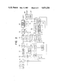
- FIG. 2 is a block diagram of an embodiment of a telephoto transmitter employing a photograph as shown in FIG. 1 in which the present invention is applied.
- a sequence controller 18 controls the operation sequence of the transmitter, and controls the rotation of the motor 12 through a motor control circuit 13 in response to the positional information of the image sensor 10 in the direction X detected by a position detector 14.
- a pre-amplifier 19 amplifies the analog electrical signals from the image sensor.
- a clamp circuit 20 is provided to shift the DC level of the signals from the pre-amplifier 19.
- a negative film gamma correcting circuit 21, an inverting circuit 22 and a positive film gamma correcting circuit 23 are controlled by a selector switch 28.
- a filter 24 modifies the signals transmitted through the switch 28 to match with the frequency band of a telephone line.
- a digital image signal processing circuit 25 is provided for example for image processing with a computer.
- a modulator 26 performs AM or FM modulation of a carrier generated from a carrier signal generator 27 with the image signals obtained through the line filter 24 for image transmission through the telephone line.
- a clock generator 29 for generating clock signals for sequence control of the apparatus; a sample hold circuit 30 for detecting optical black level; a maximum density detecting circuit 31 for detecting the maximum density value in the film image in a high-speed scanning (hereinafter called pre-scanning) preceding the scanning for photoelectric conversion for signal transmission through the telephone line or for digital image processing (hereinafter called main scanning); a minimum density detecting circuit 34 for detecting the minimum density value of the most transparent area in the film image in the pre-scanning; a diaphragm aperture calculating circuit 35 for calculating the optimum diaphragm aperture from the outputs of the maximum density detecting circuit 31 and the minimum density detecting circuit 34; a motor control circuit 36 for controlling the rotation of the diaphragm drive motor 11 in response to the output of the diaphragm aperture calculating circuit 35; and a potentiometer 37 for moving a brush to regulate resistance according to the diaphragm aperture of the diaphragm 8a.
- a clamp voltage calculating circuit 32 calculates a clamp voltage from the outputs of the sample hold circuit 30, maximum density detecting circuit 31 and diaphragm aperture calculating circuit 35 to regulate the output level of the minimum density in the main scanning to a standard level.
- a voltage hold circuit 33 holds the output voltage of said clamp voltage calculating circuit during the pre-scanning and main scanning and supplies said voltage to the clamp circuit 20.
- FIG. 3 is a wave form chart of the image signals of a horizontal scanning line obtained from the linear sensor in the pre-scanning for detecting the maximum and minimum densities of the film employed
- FIG. 4 is a wave form chart of the image signals of a horizontal scanning line obtained in the main scanning according to the present invention.
- FIG. 5 is a chart showing an example of the gamma characteristic of the negative gamma correcting circuit 21 in case a negative film is loaded
- FIG. 6 is a chart showing an example of the gamma characteristic of the positive gamma correcting circuit 23 in case a positive film is loaded.
- the sequence controller 18 Prior to the pre-scanning, the sequence controller 18 supplies a signal to the motor control circuit 36 in such a manner as to preset the aperture of the diaphragm 8a to a determined value. In this manner the saturation of the output of the linear sensor 10 can be prevented for a film of any density distribution. Then, again prior to the pre-scanning, the sequence controller 18 causes the clock pulse generator 29 to supply clock pulses to the sample hold circuit 30, thereby causing said circuit to detect the output level of a light-shielded photodiode (hereinafter called optical black photodiode) of the linear sensor 10.
- the voltage hold circuit 33 holds the voltage determined by said calculating circuit 32 and continues to supply said voltage to the clamp circuit 20 during the pre-scanning.
- the pre-scanning allows detection, by the maximum density detecting circuit 31 and the minimum density detecting circuit 34, of the maximum and minimum densities respectively of the loaded film.
- FIG. 3 shows the minimum density level a and the maximum density level b. Then the position detector 14 determines the completion of the pre-scanning of the image sensor 10.
- the clamp voltage calculating circuit 32 and the diaphragm aperture calculating circuit 35 calculate an aperture and a clamp voltage in such a manner that the minimum and maximum levels in the main scanning become respectively equal to the predetermined minimum and maximum density levels a', b' shown in FIG. 4.
- the minimum density detecting circuit 34 may be composed of a peak-hold circuit.
- the clamp circuit 20 receives the clamp voltage from the voltage hold circuit 33 and sets the maximum density level (level b in FIG. 3) of the loaded film as the reference level (level b' in FIG. 4) during the main scanning. In this manner the electrical image signals can be normalized within a determined level range for the film of any exposure status.
- the sequence controller 18 effects the main scanning, and the image signals obtained in said main scanning are supplied through the pre-amplifier 19 and the clamp circuit 20 and subjected to correction of gamma or contrast characteristics, either in the negative gamma correction circuit 21 of the gamma characteristic shown in FIG.
- the output signals of the inverting circuit 22 or the positive gamma correcting circuit 23 supplied through the switch 28 are supplied to the digital image processing circuit 25 for generating digital image signals suitable for computer processing etc. and to the telephone line filter 24.
- the output signals of said filter 24 effect AM or FM modulation of the carrier from the carrier signal generator 27 by means of a telephone line modulator 26, and the obtained signals are released from an output terminal OUT2 for the telephone line. Also the output signals of the image processing circuit 25 are released from an output terminal OUT1.
- Each of the gamma correcting circuits 21, 23 has plural gamma correcting characteristics, but the number of such correcting characteristics can be reduced since the input electrical signals are contained within a determined level range.
- the minimum density detecting circuit 34 holds the maximum peak in the output signals of the linear sensor 10 in each horizontal scanning line in the pre-scanning.
- the maximum density detecting circuit 31 holds the minimum peak in the output signals of the linear sensor 10 during a predetermined period not affected by the optical black photodiode in each horizontal scanning line.
- FIG. 7 is a block diagram showing the principal part of another embodiment
- FIG. 8 is a wave form chart similar to FIG. 3, showing the image signals of a line obtained from the linear sensor in the pre-scanning
- FIG. 9 is a chart showing the gamma characteristic for gamma correction.
- the circuit shown in the block diagram of FIG. 7 is to replace a part of the circuit shown in FIG. 2 representing the present invention, and is to be inserted between the pre-amplifier 19 and the digital image processing circuit and filter 24 shown in FIG. 2.
- the circuit shown in FIG. 7 comprises an AD converter 40; buffer amplifiers BUF1, BUF2; a random access memory 41; data selectors DS1, DS2; a positive/negative film selector switch 42; and a micro computer 43 including a central processing unit.
- a read/write port R/W There are further shown a read/write port R/W; a contact R to be selected at data read-out; a contact W to be selected at data write-in; an address port A; and a data port D.
- the D-A converter 44 converts the digital output signals of the buffer amplifier BUF2 into analog signals.
- the gamma correction curve is regulated to obtain a constant amplitude in the image signals.
- the function of the present embodiment is as follows.
- the output signals from the pre-amplifier 19 are converted into digital signals by means of the A-D converter 40.
- the data selectors DS1, DS2 are both positioned at the contacts R by the CPU 43. Consequently the digitally converted image signals are supplied to the data port D of the CPU 43. In this state the port R/W of the CPU 43 assumes the high-level state to deactivate the buffer amplifier BUF2.
- the CPU 43 detects the maximum and minimum densities of the entered image signals, namely the levels b1, a1 in FIG. 8, and determines a gamma correction curve for obtaining data b1, a1' shown in FIG. 9.
- the address and data of the thus determined gamma correction curve are supplied to the random access memory 41.
- the data selectors DS1, DS2 are shifted to the contacts W, whereby the port R/W of the CPU assumes the low-level state to deactivate the buffer BUF1.
- the address and data are supplied from the address port A and data port D of the CPU to the random access memory to store the gamma correction curve therein.
- the CPU turns on the buffers BUF1, BUF2, whereby the output signals of the A-D converter 40 are supplied to the address port A of the random access memory, and the data port D releases the data processed according to thus determined gamma correction.
Landscapes
- Engineering & Computer Science (AREA)
- Multimedia (AREA)
- Signal Processing (AREA)
- Facsimile Scanning Arrangements (AREA)
- Facsimile Image Signal Circuits (AREA)
Applications Claiming Priority (2)
| Application Number | Priority Date | Filing Date | Title |
|---|---|---|---|
| JP58-198745 | 1983-10-24 | ||
| JP58198745A JPH0773335B2 (ja) | 1983-10-24 | 1983-10-24 | 光電変換装置 |
Publications (1)
| Publication Number | Publication Date |
|---|---|
| US4651226A true US4651226A (en) | 1987-03-17 |
Family
ID=16396260
Family Applications (1)
| Application Number | Title | Priority Date | Filing Date |
|---|---|---|---|
| US06/661,829 Expired - Lifetime US4651226A (en) | 1983-10-24 | 1984-10-17 | Image scanning signal generating apparatus with pre-scan for exposure control |
Country Status (4)
| Country | Link |
|---|---|
| US (1) | US4651226A (enExample) |
| JP (1) | JPH0773335B2 (enExample) |
| DE (1) | DE3438938A1 (enExample) |
| GB (1) | GB2150392B (enExample) |
Cited By (27)
| Publication number | Priority date | Publication date | Assignee | Title |
|---|---|---|---|---|
| US4740838A (en) * | 1985-12-04 | 1988-04-26 | Aisin Seiki Kabushiki Kaisha | Apparatus for superimposing a display of detected data for a vehicle |
| US4751377A (en) * | 1985-12-27 | 1988-06-14 | Fuji Photo Film Co., Ltd. | Light beam scanning recording apparatus and method of correcting intensity of image to be recorded thereby |
| US4785357A (en) * | 1985-12-27 | 1988-11-15 | Dreyfus Bertrand A | Device for photocopying parts of documents |
| US4825065A (en) * | 1985-10-31 | 1989-04-25 | Canon Kabushiki Kaisha | Apparatus for reading image recorded on film |
| US4882629A (en) * | 1987-05-08 | 1989-11-21 | Everex Ti Corporation | Adaptive exposure control system |
| US4920429A (en) * | 1989-01-24 | 1990-04-24 | International Business Machines | Exposure compensation for a line scan camera |
| US4922335A (en) * | 1986-11-14 | 1990-05-01 | Canon Kabushiki Kaisha | Color film reading apparatus providing high-gradation color signals |
| US4949391A (en) * | 1986-09-26 | 1990-08-14 | Everex Ti Corporation | Adaptive image acquisition system |
| US4963962A (en) * | 1989-01-25 | 1990-10-16 | Visual Methods, Inc. | Optical surveillance assembly and camera |
| US4980776A (en) * | 1989-03-31 | 1990-12-25 | Fuji Photo Film Co., Ltd. | Electronic copying machine having a line sensor in which the charge storage time is set based on image signals of the previous scan line |
| US5128769A (en) * | 1989-07-18 | 1992-07-07 | Fuji Photo Film Co., Ltd. | Method and apparatus for controlling exposure of video camera |
| US5162645A (en) * | 1990-02-16 | 1992-11-10 | Agfa-Gevaert Aktiengesellschaft | Photographic scanner with reduced susceptibility to scattering |
| US5424774A (en) * | 1990-05-02 | 1995-06-13 | Canon Kabushiki Kaisha | Image sensing apparatus |
| US5612794A (en) * | 1990-04-20 | 1997-03-18 | Nikon Corporation | Light source for an image reading device |
| US5706050A (en) * | 1993-12-24 | 1998-01-06 | Fuji Photo Film Co., Ltd. | Film image input method and system thereof |
| US5778878A (en) * | 1994-06-04 | 1998-07-14 | Kellam; Keith | Laser doppler microscopy methods and instruments |
| US5946109A (en) * | 1996-06-21 | 1999-08-31 | Nikon Corporation | Picture image input method |
| US5978103A (en) * | 1995-06-30 | 1999-11-02 | Crw Imaging Inc. | Apparatus and method for computerized acquisition of x-ray images |
| EP1176800A3 (en) * | 2000-07-28 | 2004-08-04 | Ricoh Company, Ltd. | Image reading method, image reader, image reader controlling method and image processing system using improved peak correction |
| US20060119903A1 (en) * | 2004-11-11 | 2006-06-08 | Takuma Chiba | Imaging apparatus and imaging method |
| US20080217516A1 (en) * | 2004-07-22 | 2008-09-11 | Hamamatsu Photonics K.K. | Photodetector |
| US20140163319A1 (en) * | 2012-07-26 | 2014-06-12 | Olive Medical Corporation | Continuous video in a light deficient environment |
| US9516239B2 (en) | 2012-07-26 | 2016-12-06 | DePuy Synthes Products, Inc. | YCBCR pulsed illumination scheme in a light deficient environment |
| US9641815B2 (en) | 2013-03-15 | 2017-05-02 | DePuy Synthes Products, Inc. | Super resolution and color motion artifact correction in a pulsed color imaging system |
| US9777913B2 (en) | 2013-03-15 | 2017-10-03 | DePuy Synthes Products, Inc. | Controlling the integral light energy of a laser pulse |
| US10084944B2 (en) | 2014-03-21 | 2018-09-25 | DePuy Synthes Products, Inc. | Card edge connector for an imaging sensor |
| US10251530B2 (en) | 2013-03-15 | 2019-04-09 | DePuy Synthes Products, Inc. | Scope sensing in a light controlled environment |
Families Citing this family (4)
| Publication number | Priority date | Publication date | Assignee | Title |
|---|---|---|---|---|
| DE3760646D1 (en) * | 1987-03-13 | 1989-11-02 | Hell Rudolf Dr Ing Gmbh | Method and apparatus for white-level adjustment |
| US4912558A (en) * | 1988-12-27 | 1990-03-27 | Eastman Kodak Company | Optical image to video transfer system having enhanced resolution and contrast for dark areas of the image |
| US5038216A (en) * | 1989-04-20 | 1991-08-06 | Eastman Kodak Company | Automatic brightness algorithm in a slide to video transfer unit |
| AT399059B (de) * | 1992-12-03 | 1995-03-27 | Tabarelli Werner | Bildwandlungseinrichtung |
Citations (5)
| Publication number | Priority date | Publication date | Assignee | Title |
|---|---|---|---|---|
| US3624291A (en) * | 1968-12-28 | 1971-11-30 | Olympus Optical Co | Optically interlaced scanning and reproducing apparatus using multiple drums to permit scanning of motion picture film or stationary film |
| US3804976A (en) * | 1972-05-15 | 1974-04-16 | Kaiser Aerospace & Electronics | Multiplexed infrared imaging system |
| US3931464A (en) * | 1973-11-01 | 1976-01-06 | Ricoh Co., Ltd. | Line skip system for facsimile device |
| US4158859A (en) * | 1977-07-25 | 1979-06-19 | Hazeltine Corporation | Automatic control of iris and clamping voltage in video signal generator |
| US4255764A (en) * | 1979-08-20 | 1981-03-10 | Eastman Kodak Company | Film scanner employing optical splice technique for frame-rate conversion |
Family Cites Families (12)
| Publication number | Priority date | Publication date | Assignee | Title |
|---|---|---|---|---|
| JPS5323506A (en) * | 1976-08-18 | 1978-03-04 | Ricoh Co Ltd | Reading system |
| DE2654943C2 (de) * | 1976-12-03 | 1985-10-24 | Agfa-Gevaert Ag, 5090 Leverkusen | Verfahren und Vorrichtung zur Vorprüfung von zu einem Vorlagenband zusammengefaßten Kopiervorlagen |
| DE2717685C3 (de) * | 1977-04-21 | 1981-04-02 | Audi Nsu Auto Union Ag, 7107 Neckarsulm | Brennkraftmaschine für Kraftfahrzeuge |
| JPS5560826A (en) * | 1978-11-01 | 1980-05-08 | Olympus Optical Co Ltd | Photometry |
| JPS5660165A (en) * | 1979-10-20 | 1981-05-23 | Canon Inc | Picture reader |
| US4329717A (en) * | 1980-02-11 | 1982-05-11 | Exxon Research & Engineering Co. | Facsimile method and apparatus for setting white level |
| JPS57208768A (en) * | 1981-06-19 | 1982-12-21 | Hitachi Ltd | Digitizing system for video signal |
| JPS5839168A (ja) * | 1981-09-02 | 1983-03-07 | Ricoh Co Ltd | ガンマ補正装置 |
| JPS58156260A (ja) * | 1982-03-12 | 1983-09-17 | Canon Inc | 画像読取り装置 |
| JPS58178665A (ja) * | 1982-04-12 | 1983-10-19 | Canon Inc | 画像処理装置 |
| JPH0757006B2 (ja) * | 1983-08-09 | 1995-06-14 | 富士写真フイルム株式会社 | 階調変換テーブルの自動設定方式 |
| JP2501782B2 (ja) * | 1983-09-16 | 1996-05-29 | 株式会社ニコン | 画像走査装置 |
-
1983
- 1983-10-24 JP JP58198745A patent/JPH0773335B2/ja not_active Expired - Lifetime
-
1984
- 1984-10-17 US US06/661,829 patent/US4651226A/en not_active Expired - Lifetime
- 1984-10-24 DE DE19843438938 patent/DE3438938A1/de active Granted
- 1984-10-24 GB GB08426868A patent/GB2150392B/en not_active Expired
Patent Citations (5)
| Publication number | Priority date | Publication date | Assignee | Title |
|---|---|---|---|---|
| US3624291A (en) * | 1968-12-28 | 1971-11-30 | Olympus Optical Co | Optically interlaced scanning and reproducing apparatus using multiple drums to permit scanning of motion picture film or stationary film |
| US3804976A (en) * | 1972-05-15 | 1974-04-16 | Kaiser Aerospace & Electronics | Multiplexed infrared imaging system |
| US3931464A (en) * | 1973-11-01 | 1976-01-06 | Ricoh Co., Ltd. | Line skip system for facsimile device |
| US4158859A (en) * | 1977-07-25 | 1979-06-19 | Hazeltine Corporation | Automatic control of iris and clamping voltage in video signal generator |
| US4255764A (en) * | 1979-08-20 | 1981-03-10 | Eastman Kodak Company | Film scanner employing optical splice technique for frame-rate conversion |
Cited By (50)
| Publication number | Priority date | Publication date | Assignee | Title |
|---|---|---|---|---|
| US4825065A (en) * | 1985-10-31 | 1989-04-25 | Canon Kabushiki Kaisha | Apparatus for reading image recorded on film |
| US4740838A (en) * | 1985-12-04 | 1988-04-26 | Aisin Seiki Kabushiki Kaisha | Apparatus for superimposing a display of detected data for a vehicle |
| US4751377A (en) * | 1985-12-27 | 1988-06-14 | Fuji Photo Film Co., Ltd. | Light beam scanning recording apparatus and method of correcting intensity of image to be recorded thereby |
| US4785357A (en) * | 1985-12-27 | 1988-11-15 | Dreyfus Bertrand A | Device for photocopying parts of documents |
| US4949391A (en) * | 1986-09-26 | 1990-08-14 | Everex Ti Corporation | Adaptive image acquisition system |
| US4922335A (en) * | 1986-11-14 | 1990-05-01 | Canon Kabushiki Kaisha | Color film reading apparatus providing high-gradation color signals |
| US4882629A (en) * | 1987-05-08 | 1989-11-21 | Everex Ti Corporation | Adaptive exposure control system |
| US4920429A (en) * | 1989-01-24 | 1990-04-24 | International Business Machines | Exposure compensation for a line scan camera |
| US4963962A (en) * | 1989-01-25 | 1990-10-16 | Visual Methods, Inc. | Optical surveillance assembly and camera |
| US4980776A (en) * | 1989-03-31 | 1990-12-25 | Fuji Photo Film Co., Ltd. | Electronic copying machine having a line sensor in which the charge storage time is set based on image signals of the previous scan line |
| US5128769A (en) * | 1989-07-18 | 1992-07-07 | Fuji Photo Film Co., Ltd. | Method and apparatus for controlling exposure of video camera |
| US5162645A (en) * | 1990-02-16 | 1992-11-10 | Agfa-Gevaert Aktiengesellschaft | Photographic scanner with reduced susceptibility to scattering |
| US5612794A (en) * | 1990-04-20 | 1997-03-18 | Nikon Corporation | Light source for an image reading device |
| US5684610A (en) * | 1990-04-20 | 1997-11-04 | Nikon Corporation | Method and apparatus for rapid scanning of color images |
| US5724160A (en) * | 1990-04-20 | 1998-03-03 | Nikon Corporation | Optical scanner for line scanning an original |
| US6044180A (en) * | 1990-04-20 | 2000-03-28 | Nec Corporation | Method and apparatus for rapid scanning of color images |
| US5424774A (en) * | 1990-05-02 | 1995-06-13 | Canon Kabushiki Kaisha | Image sensing apparatus |
| US5706050A (en) * | 1993-12-24 | 1998-01-06 | Fuji Photo Film Co., Ltd. | Film image input method and system thereof |
| US5778878A (en) * | 1994-06-04 | 1998-07-14 | Kellam; Keith | Laser doppler microscopy methods and instruments |
| US5978103A (en) * | 1995-06-30 | 1999-11-02 | Crw Imaging Inc. | Apparatus and method for computerized acquisition of x-ray images |
| US5946109A (en) * | 1996-06-21 | 1999-08-31 | Nikon Corporation | Picture image input method |
| EP1176800A3 (en) * | 2000-07-28 | 2004-08-04 | Ricoh Company, Ltd. | Image reading method, image reader, image reader controlling method and image processing system using improved peak correction |
| US7605358B2 (en) * | 2004-07-22 | 2009-10-20 | Hamamatsu Photonics K.K. | Photodetector having dual photodiode and gain adjusting amplifiers |
| US20080217516A1 (en) * | 2004-07-22 | 2008-09-11 | Hamamatsu Photonics K.K. | Photodetector |
| US20060119903A1 (en) * | 2004-11-11 | 2006-06-08 | Takuma Chiba | Imaging apparatus and imaging method |
| US7876980B2 (en) * | 2004-11-11 | 2011-01-25 | Panasonic Corporation | Imaging apparatus and imaging method for outputting a specified number of pixels in a specified area |
| US11070779B2 (en) | 2012-07-26 | 2021-07-20 | DePuy Synthes Products, Inc. | YCBCR pulsed illumination scheme in a light deficient environment |
| US10568496B2 (en) * | 2012-07-26 | 2020-02-25 | DePuy Synthes Products, Inc. | Continuous video in a light deficient environment |
| US9516239B2 (en) | 2012-07-26 | 2016-12-06 | DePuy Synthes Products, Inc. | YCBCR pulsed illumination scheme in a light deficient environment |
| US11863878B2 (en) | 2012-07-26 | 2024-01-02 | DePuy Synthes Products, Inc. | YCBCR pulsed illumination scheme in a light deficient environment |
| US9762879B2 (en) | 2012-07-26 | 2017-09-12 | DePuy Synthes Products, Inc. | YCbCr pulsed illumination scheme in a light deficient environment |
| US11083367B2 (en) * | 2012-07-26 | 2021-08-10 | DePuy Synthes Products, Inc. | Continuous video in a light deficient environment |
| US20140163319A1 (en) * | 2012-07-26 | 2014-06-12 | Olive Medical Corporation | Continuous video in a light deficient environment |
| US10785461B2 (en) | 2012-07-26 | 2020-09-22 | DePuy Synthes Products, Inc. | YCbCr pulsed illumination scheme in a light deficient environment |
| US20160183775A1 (en) * | 2012-07-26 | 2016-06-30 | DePuy Synthes Products, Inc. | Continuous video in a light deficient environment |
| US10277875B2 (en) | 2012-07-26 | 2019-04-30 | DePuy Synthes Products, Inc. | YCBCR pulsed illumination scheme in a light deficient environment |
| US10670248B2 (en) | 2013-03-15 | 2020-06-02 | DePuy Synthes Products, Inc. | Controlling the integral light energy of a laser pulse |
| US11185213B2 (en) | 2013-03-15 | 2021-11-30 | DePuy Synthes Products, Inc. | Scope sensing in a light controlled environment |
| US10205877B2 (en) | 2013-03-15 | 2019-02-12 | DePuy Synthes Products, Inc. | Super resolution and color motion artifact correction in a pulsed color imaging system |
| US12231784B2 (en) | 2013-03-15 | 2025-02-18 | DePuy Synthes Products, Inc. | Super resolution and color motion artifact correction in a pulsed color imaging system |
| US10917562B2 (en) | 2013-03-15 | 2021-02-09 | DePuy Synthes Products, Inc. | Super resolution and color motion artifact correction in a pulsed color imaging system |
| US11974717B2 (en) | 2013-03-15 | 2024-05-07 | DePuy Synthes Products, Inc. | Scope sensing in a light controlled environment |
| US9777913B2 (en) | 2013-03-15 | 2017-10-03 | DePuy Synthes Products, Inc. | Controlling the integral light energy of a laser pulse |
| US10251530B2 (en) | 2013-03-15 | 2019-04-09 | DePuy Synthes Products, Inc. | Scope sensing in a light controlled environment |
| US9641815B2 (en) | 2013-03-15 | 2017-05-02 | DePuy Synthes Products, Inc. | Super resolution and color motion artifact correction in a pulsed color imaging system |
| US11674677B2 (en) | 2013-03-15 | 2023-06-13 | DePuy Synthes Products, Inc. | Controlling the integral light energy of a laser pulse |
| US11438490B2 (en) | 2014-03-21 | 2022-09-06 | DePuy Synthes Products, Inc. | Card edge connector for an imaging sensor |
| US10084944B2 (en) | 2014-03-21 | 2018-09-25 | DePuy Synthes Products, Inc. | Card edge connector for an imaging sensor |
| US10911649B2 (en) | 2014-03-21 | 2021-02-02 | DePuy Synthes Products, Inc. | Card edge connector for an imaging sensor |
| US12309473B2 (en) | 2014-03-21 | 2025-05-20 | DePuy Synthes Products, Inc. | Card edge connector for an imaging sensor |
Also Published As
| Publication number | Publication date |
|---|---|
| DE3438938C2 (enExample) | 1993-07-08 |
| GB2150392A (en) | 1985-06-26 |
| GB8426868D0 (en) | 1984-11-28 |
| GB2150392B (en) | 1988-02-10 |
| JPS6090466A (ja) | 1985-05-21 |
| DE3438938A1 (de) | 1985-05-02 |
| JPH0773335B2 (ja) | 1995-08-02 |
Similar Documents
| Publication | Publication Date | Title |
|---|---|---|
| US4651226A (en) | Image scanning signal generating apparatus with pre-scan for exposure control | |
| US5084772A (en) | Shading correcting method in image reading device | |
| GB2063615A (en) | Black level clamp for solid state pick up | |
| US4734783A (en) | Shading elimination device for image read-out apparatus | |
| JPH03209441A (ja) | 光走査装置 | |
| JPH01240070A (ja) | 画像読取記録装置 | |
| US4674126A (en) | Image signal processing apparatus | |
| US4689690A (en) | Synchronizing signal generating circuit | |
| US4755875A (en) | Telecine apparatus including an electro-optical image transducer illuminated by a bias light source | |
| JPH10210208A5 (enExample) | ||
| JPH02280460A (ja) | 画像記録装置 | |
| US5220626A (en) | Method of smoothly combining signals from overlapping sensors | |
| JP2621065B2 (ja) | 光電変換装置 | |
| JPH0341876A (ja) | 画像信号補正方法 | |
| JPH03212064A (ja) | 画像読取装置 | |
| EP0569063B1 (en) | Automatic offset and gain control in a document scanner | |
| JP3112962B2 (ja) | 画像読取装置 | |
| JP2618923B2 (ja) | 原稿読取装置 | |
| JPS62257279A (ja) | フイルム画像読取装置 | |
| JP2590851B2 (ja) | 情報読取り装置 | |
| JPH065860B2 (ja) | イメ−ジリ−ダ−用オ−トフオ−カス機構 | |
| JPS59223060A (ja) | 原稿読取装置 | |
| JPS6158374A (ja) | 画像読取り装置 | |
| JPS61208370A (ja) | 光電変換装置 | |
| JPH02211771A (ja) | 画像信号処理方法 |
Legal Events
| Date | Code | Title | Description |
|---|---|---|---|
| AS | Assignment |
Owner name: KYODO NEWS SERIVCE 2-5, TORANOMON 2-CHOME, MINATO- Free format text: ASSIGNMENT OF ASSIGNORS INTEREST.;ASSIGNORS:MOTOORI, RYUZO;KIMURA, MAKOTO;ISOGAI, MASAKI;AND OTHERS;REEL/FRAME:004326/0260 Effective date: 19841015 Owner name: NIPPON KOGAKU K.K. 2-3 MARUNOUCHI 3-CHOME MINATO-K Free format text: ASSIGNMENT OF ASSIGNORS INTEREST.;ASSIGNORS:MOTOORI, RYUZO;KIMURA, MAKOTO;ISOGAI, MASAKI;AND OTHERS;REEL/FRAME:004326/0260 Effective date: 19841015 |
|
| STCF | Information on status: patent grant |
Free format text: PATENTED CASE |
|
| AS | Assignment |
Owner name: NIKON CORPORATION, 2-3, MARUNOUCHI 3-CHOME, CHIYOD Free format text: CHANGE OF NAME;ASSIGNOR:NIPPON KOGAKU, K.K.;REEL/FRAME:004935/0584 |
|
| FPAY | Fee payment |
Year of fee payment: 4 |
|
| FEPP | Fee payment procedure |
Free format text: PAYOR NUMBER ASSIGNED (ORIGINAL EVENT CODE: ASPN); ENTITY STATUS OF PATENT OWNER: LARGE ENTITY |
|
| FPAY | Fee payment |
Year of fee payment: 8 |
|
| AS | Assignment |
Owner name: NIKON CORPORATION, JAPAN Free format text: ASSIGNMENT OF ASSIGNORS INTEREST;ASSIGNOR:KYODO NEWS SERVICE;REEL/FRAME:008423/0807 Effective date: 19970304 |
|
| FEPP | Fee payment procedure |
Free format text: PAYER NUMBER DE-ASSIGNED (ORIGINAL EVENT CODE: RMPN); ENTITY STATUS OF PATENT OWNER: LARGE ENTITY Free format text: PAYOR NUMBER ASSIGNED (ORIGINAL EVENT CODE: ASPN); ENTITY STATUS OF PATENT OWNER: LARGE ENTITY |
|
| FPAY | Fee payment |
Year of fee payment: 12 |