EP0569063B1 - Automatic offset and gain control in a document scanner - Google Patents
Automatic offset and gain control in a document scanner Download PDFInfo
- Publication number
- EP0569063B1 EP0569063B1 EP93200882A EP93200882A EP0569063B1 EP 0569063 B1 EP0569063 B1 EP 0569063B1 EP 93200882 A EP93200882 A EP 93200882A EP 93200882 A EP93200882 A EP 93200882A EP 0569063 B1 EP0569063 B1 EP 0569063B1
- Authority
- EP
- European Patent Office
- Prior art keywords
- calibration
- signal
- density
- offset
- document
- Prior art date
- Legal status (The legal status is an assumption and is not a legal conclusion. Google has not performed a legal analysis and makes no representation as to the accuracy of the status listed.)
- Expired - Lifetime
Links
Images


Classifications
-
- H—ELECTRICITY
- H04—ELECTRIC COMMUNICATION TECHNIQUE
- H04N—PICTORIAL COMMUNICATION, e.g. TELEVISION
- H04N1/00—Scanning, transmission or reproduction of documents or the like, e.g. facsimile transmission; Details thereof
- H04N1/40—Picture signal circuits
- H04N1/407—Control or modification of tonal gradation or of extreme levels, e.g. background level
- H04N1/4076—Control or modification of tonal gradation or of extreme levels, e.g. background level dependent on references outside the picture
-
- H—ELECTRICITY
- H04—ELECTRIC COMMUNICATION TECHNIQUE
- H04N—PICTORIAL COMMUNICATION, e.g. TELEVISION
- H04N25/00—Circuitry of solid-state image sensors [SSIS]; Control thereof
- H04N25/60—Noise processing, e.g. detecting, correcting, reducing or removing noise
- H04N25/63—Noise processing, e.g. detecting, correcting, reducing or removing noise applied to dark current
-
- H—ELECTRICITY
- H04—ELECTRIC COMMUNICATION TECHNIQUE
- H04N—PICTORIAL COMMUNICATION, e.g. TELEVISION
- H04N25/00—Circuitry of solid-state image sensors [SSIS]; Control thereof
- H04N25/60—Noise processing, e.g. detecting, correcting, reducing or removing noise
- H04N25/67—Noise processing, e.g. detecting, correcting, reducing or removing noise applied to fixed-pattern noise, e.g. non-uniformity of response
- H04N25/671—Noise processing, e.g. detecting, correcting, reducing or removing noise applied to fixed-pattern noise, e.g. non-uniformity of response for non-uniformity detection or correction
-
- H—ELECTRICITY
- H04—ELECTRIC COMMUNICATION TECHNIQUE
- H04N—PICTORIAL COMMUNICATION, e.g. TELEVISION
- H04N25/00—Circuitry of solid-state image sensors [SSIS]; Control thereof
- H04N25/70—SSIS architectures; Circuits associated therewith
- H04N25/701—Line sensors
Definitions
- the present invention relates to the field of electro-optical scanning and provides a method for correcting, on an individual pixel basis, all unwanted offset and/or gain variations in the input signal representing the shade of darkness or light-ness of the source document.
- a source document is scanned line by line by a narrowly focused light beam.
- the light reflected from the scanned document is collected by a suitable photosensor to produce a corresponding video signal whose voltage is representative of the shade of darkness or lightness of the document, hereinafter called "source signal”.
- the actual offset and amplitude of the source signal is subject to variations in accordance with such factors as variations in the intensity of the illuminating light beam, drift of the photosensors due to aging or temperature change, drift in the electronic circuits, and many other factors.
- a calibration scan is executed, in which the unit acquires black and white samples of the source signal produced by the photosensors in response to the illumination of a black-white scanning strip by the scanning beam.
- Black and white are designated by the reflectance signal obtained from a "calibration strip", also called “target”, and located mostly adjacent to the image scanning area.
- a calibration strip may be as well throughput in the form of a calibration sheet, or it may be temporarily turned in the optical scanning path of the apparatus (as e. g. published by Hanna and Melamud, in IBM Technical Disclosure Bulletin, vol. . 21. no.4, september 1978, p. 1410).
- the first half of the strip may be imprinted black, or may be absent but replaced by a control signal which turns the lighting beam off e.g. by closing the lens aperture.
- the second half of the strip may be imprinted white or be apertured with a clear open gate to expose a nominally white background area of the document; or a so-called "Dmin" filter, which is a filter having a density corresponding to a calibrated white reference density, may be introduced in the optical path of the scan-apparatus.
- the apparatus will process the variable input signals V in as exact representatives V corr of the reflective gradations in shades of grey in the original. Even, if the lowest density-value of the source signal eventually could reach extremely low values, e.g. below the low calibration level as Vmin ⁇ Vin ⁇ Vw.
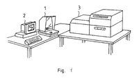
- Figure 1 generally shows a system in which the method of the invention can be applied.
- the scanning and digitising apparatus of figure 1 comprises as main subparts : a viewer or workstation 1, a microprocessor 2, a scanner 3 and possibly a printer or a recorder (not indicated in fig. 1).
- the devices are interconnected via suitable electronic interfaces.
- Information which can be read by such scanner includes information from a reflective or transparent document, a photograph, a film sheet, a map , a table, a character, a symbol and the like. In addition, pattern recognition of a flat object is also included. These info-carriers are further called source documents.
- a scanning device of the above-named kind essentially comprises a platen for carrying an image to be scanned. a light-source for illuminating said image, means for directing image-wise modulated light onto an opto-electronic sensor, such as a CCD sensor, and signal digitising means.
- document scanners which comprise a bodily stationary document supporting plate and a scanning unit which is mounted for bodily movement parallel with the plate.
- a light image of a line across the document is focused within the unit into the optical sensing means so that the document is scanned line by line during a scanning displacement of the unit.
- Document scanners are also known which differ from those just referred to in that the scanning unit is fixed and the document supporting plate is mounted for movement relative to said unit.
- feedtrough scanners in which the source document passes a scanning station under well-defined circumstances (as to optical path, moving velocity, etc).
- Figure 2 shows a colour scanner comprising a light source 1 for projecting scanning light towards an image plane and a work support 2 for supporting an image-bearing sheet 3 in said image plane.
- Said light source 1 and said support 2 are relatively displaced by means of a suitable drive mechanism that is not shown in this figure.
- a filterwheel 4 is provided for separating white light emitted by the light source 1 into colour components and transmission fibres 5 are provided for directing scanner radiation to the image plane.
- the scanner further comprises suitable optics (11 to 15) for directing image-wise modulated light to an opto-electronic sensor 16, for example a CCD sensor, and means for converting the image-wise radiation into a digitised signal (not shown on the figure).
- a document may be printed in blue ink on a light green background.
- variable input signal In order to accurately and reliably reproduce shades of grey that may be present in such original, at least a minimal distance between the variable input signal and a reference level must be established.
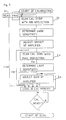
- Said method commonly called calibration procedure, consists of several steps, executed prior to substantially every document scan, and will be explained consecutively in the following paragraphs (with reference to figs 3, 4 and 5).
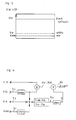
- a white level reference for the maximum whitness which has to be managed by the scanning apparatus. So, in a first step S1 (see fig. 4 and fig. 5), we define a minimal reference density value Vmin (see also fig. 3), representative of the whitest or lowest possible density value which could possibly occur in the actual source document to be scanned.
- the apparatus scans the calibration signal at high density-level, equivalent to the minimum reflection by the black area of a calibration strip. After reading a sample V bl of said calibration signal when said density-value is at its highest level, this value is stored as an offset-value in a calibration memory. More specifically, this offset-value is the lowest level of illumination that a sensor cell could experience during a document scan and by the present method, while calibrating, all possible variations in the dark-current are corrected.
- a third step S3 the apparatus scans the low density-level Vw of the calibration signal in order to correct for variations in the shading, by scanning the white part of the strip.
- a fourth step S4 the amplifier is adapted to the point at which the max output of said amplifier is just equal to the reference level V min , as may be controlled by an usual electronic comparator.
- the apparatus is really capable of starting the ultimate scanning process by determination of the signal strength of the variable input signal V in compared to the reflectance level of the reference.
- the apparatus will process the variable input signals V in as exact representatives V corr of the reflective gradations in shades of grey in the original. Even, if the lowest value of the source signal eventually could reach extremely low values, e.g. on or below the highest calibration level as with V min ⁇ V in ⁇ V w .
- Figures 4 and 5 recapitulate the presented calibration method, respectively in a principal block diagram and in a flowchart. Remark that the automatic offset and gain control is applied in a dynamic manner at the beginning of each and every document scan. A calibration operation is thus performed, prior to reading a document, by determining offset and gain for each of the pixel-related amplifiers on the basis of reference signals, mostly generated by reading a black and white reference plate, commonly called calibration strip. The determined offset and gains are stored in a suitable calibration memory.
- Figure 6 is a principal scheme of a preferred embodiment of the present invention. Some (e.g. gating) circuit is not shown in this figure for purposes of simplicity.
- sensor area 1 is a linear CCD having a line of multiple, e.g. 5000 photoelectric conversion elements, which can distinguish 400 pixels per inch on the document, by which the optical input is converted into an electric signal, in this text referred to as "source signal”.
- an amplifier 3 with an adjustable offset and gain 2 is provided for each of the CCD-line sensors 1 .
- the effective document scanning begins and original exposure is started.
- the analog electrical signal content of the sensor array is perodically read out, pixel by pixel and row by row.
- the outputs from the CCD's 1 are corrected by the obtained offset and gains (ref 2 in Fig.6), with the positive result that the signal 4 at the output of the amplifier 3 varies exactly in correspondance with the variations in reflectance of the scanned original.
- zero voltage or a minimum voltage might correspond to a white portion; a maximum voltage would correspond to a black area and intermediate volt to various shades of grey (see also fig. 3).
- Figure 7 gives an alternative preferred embodiment of the present invention.
- part of the analog circuit has been replaced by means for causing the output of the sensor 1 to convert into a digital signal through an A/D converter 5, thereafter calibrating an amplifier 3 with adjustable offset and gain and causing this digitised calibration signal to store in a digital memory 6 as e.g. a random access memory or RAM.
- a digital memory 6 as e.g. a random access memory or RAM.
- the analog signal received from each pixel-element 1 is applied to the input of an analog to digital convertor 5.
- the thus generated conversion for each original pixel may be a multi-bit digital signal, which allows the sensing of different levels of blackness within each pixel.
- the present invention is largely universal, e.g. it may be applied successivefully to scanners with moving platen for carrying the source original, to scanners with stationary platen but moving optics, as well as to feedthrough scanners.
- the present invention may also be applied for scanning of so-called "inverse-setted or mirrored" source originals, presenting light characters on a dark paper or carrier-background.
- the method according to the present invention may be iterated pro colour selection.
- the same said calibration strip is then scanned consecutively through means of colour-typical filters with suitable characteristics concerning spectral transmission and absorption.
- the invention as described above relates to a method for correcting unwanted offset and/or gain variations suitable for being used in a graphical scanning system, it may also be employed in document management application or in a scanning system suitable for use in medical or industrial, e.g. non-destructive testing, diagnostic applications.
Description
Document scanners are also known which differ from those just referred to in that the scanning unit is fixed and the document supporting plate is mounted for movement relative to said unit.
Also known are feedtrough scanners in which the source document passes a scanning station under well-defined circumstances (as to optical path, moving velocity, etc).
gain
Herein,
After said calibration conform to the present invention and the results of which are stored for future retrieval in a so-called
The outputs from the CCD's 1 are corrected by the obtained offset and gains (
As the document pixels are read, the analog signal received from each pixel-
In these applications the wording "density of a source document" has to be interpreted as "light reflected by or transmitted through a source original" and still remains under the same scope and protection of the present invention.
Claims (5)
- Method for processing a variable data-signal representative of the density of a source document, that has been scanned by a lightbeam and the reflected or transmitted light of which has been collected by at least one sensor element, said method comprising the following pixel-related steps:a) defining a minimum value Vmin , representative of the lowest possible density value which could possibly occur in the source document to be scanned;b) reading from a calibration reference having a high and a low level density a sample Vbl of the data-signal when said density-value is at its high level and storing this value as offset in a calibration memoryc) reading from a calibration reference a second sample Vw of said data-signal when said density-value is at its low level;d) dividing (Vmin -Vbl) by (Vw-Vbl) and permanently storing the quotient as a gainfactor G in said calibration memory, wheree) reading the signal values by scanning the source document, immediately corrected for offset by subtracting (Vin-Vbl) and continually combining the offset-corrected input values by multiplying with the precalculated gainfactor available from the calibration memory G, so as to form
- A method according to claim 1 wherein said calibration reference is a calibration strip consisting of a predetermined black area and a predetermined white area.
- A method according to claim 2 wherein said black and white areas are established on the face of a calibration strip which is positioned outside the area of the document being scanned.
- A method according to claim 1 wherein said calibration reference is a set of preprogrammed calibration values.
- A method according to claim 1, characterised in that the sensor element is a CCD-element.
Priority Applications (1)
| Application Number | Priority Date | Filing Date | Title |
|---|---|---|---|
| EP93200882A EP0569063B1 (en) | 1992-05-04 | 1993-03-27 | Automatic offset and gain control in a document scanner |
Applications Claiming Priority (3)
| Application Number | Priority Date | Filing Date | Title |
|---|---|---|---|
| EP92201227 | 1992-05-04 | ||
| EP92201227 | 1992-05-04 | ||
| EP93200882A EP0569063B1 (en) | 1992-05-04 | 1993-03-27 | Automatic offset and gain control in a document scanner |
Publications (2)
| Publication Number | Publication Date |
|---|---|
| EP0569063A1 EP0569063A1 (en) | 1993-11-10 |
| EP0569063B1 true EP0569063B1 (en) | 1998-06-03 |
Family
ID=26131368
Family Applications (1)
| Application Number | Title | Priority Date | Filing Date |
|---|---|---|---|
| EP93200882A Expired - Lifetime EP0569063B1 (en) | 1992-05-04 | 1993-03-27 | Automatic offset and gain control in a document scanner |
Country Status (1)
| Country | Link |
|---|---|
| EP (1) | EP0569063B1 (en) |
Families Citing this family (2)
| Publication number | Priority date | Publication date | Assignee | Title |
|---|---|---|---|---|
| US5789622A (en) * | 1996-09-12 | 1998-08-04 | Trw Inc. | Focal plane array calibration method |
| US6912003B1 (en) | 1997-07-07 | 2005-06-28 | Institute For Mikroelektronik | Methods of and circuit array for compensating variations induced by temperature strain and manufacture in CMOS video sensors |
Family Cites Families (2)
| Publication number | Priority date | Publication date | Assignee | Title |
|---|---|---|---|---|
| US3952144A (en) | 1974-10-02 | 1976-04-20 | Faxon Communications Corporation | Methods and apparatus for automatic background and contrast control |
| JPS6153868A (en) * | 1984-08-24 | 1986-03-17 | Dainippon Screen Mfg Co Ltd | Calibration in picture scan signal processing |
-
1993
- 1993-03-27 EP EP93200882A patent/EP0569063B1/en not_active Expired - Lifetime
Also Published As
| Publication number | Publication date |
|---|---|
| EP0569063A1 (en) | 1993-11-10 |
Similar Documents
| Publication | Publication Date | Title |
|---|---|---|
| EP0562814B1 (en) | Optical image defocus correction | |
| EP0439357B1 (en) | Method and apparatus for providing sensor compensation in a document scanner | |
| US5331428A (en) | Automatic offset and gain control in a document scanner | |
| US6587224B1 (en) | Image reading apparatus that can correct chromatic aberration caused by optical system and chromatic aberration correction method | |
| US4520395A (en) | System for correcting shading or non-uniformity in a photosensitive element array | |
| EP0590559B1 (en) | Image reading apparatus | |
| EP0868072B1 (en) | Shading correction for an image scanner | |
| US6038038A (en) | Method for determining offset and gain correction for a light sensitive sensor | |
| US5075768A (en) | Method and apparatus for color separation scanning | |
| US4837450A (en) | Apparatus for reading a film image with controllable illumination and threshold value | |
| EP0363969B1 (en) | Color image reading apparatus | |
| US5084772A (en) | Shading correcting method in image reading device | |
| US4734783A (en) | Shading elimination device for image read-out apparatus | |
| EP0211070B1 (en) | Dynamic gain adjuster for an image scanner | |
| US5014332A (en) | Image reader | |
| US6175660B1 (en) | Image reading apparatus | |
| US6525764B2 (en) | Image read method for performing image signal processes complying with the color of a reference portion of a recording medium, and image read apparatus adopting the method | |
| US6618512B1 (en) | Image reading apparatus | |
| US7173743B2 (en) | Image reading apparatus and method | |
| US6891645B1 (en) | Image reading apparatus and image reading method | |
| US6339466B1 (en) | Image processing apparatus | |
| EP0569063B1 (en) | Automatic offset and gain control in a document scanner | |
| US20020185616A1 (en) | Detection and correction of defects from scanner calibration references | |
| US6806870B1 (en) | Image display control apparatus including adjustment based on brightness | |
| US5220626A (en) | Method of smoothly combining signals from overlapping sensors |
Legal Events
| Date | Code | Title | Description |
|---|---|---|---|
| PUAI | Public reference made under article 153(3) epc to a published international application that has entered the european phase |
Free format text: ORIGINAL CODE: 0009012 |
|
| AK | Designated contracting states |
Kind code of ref document: A1 Designated state(s): BE DE FR GB NL |
|
| 17P | Request for examination filed |
Effective date: 19940409 |
|
| 17Q | First examination report despatched |
Effective date: 19960524 |
|
| GRAG | Despatch of communication of intention to grant |
Free format text: ORIGINAL CODE: EPIDOS AGRA |
|
| GRAG | Despatch of communication of intention to grant |
Free format text: ORIGINAL CODE: EPIDOS AGRA |
|
| GRAH | Despatch of communication of intention to grant a patent |
Free format text: ORIGINAL CODE: EPIDOS IGRA |
|
| GRAH | Despatch of communication of intention to grant a patent |
Free format text: ORIGINAL CODE: EPIDOS IGRA |
|
| GRAA | (expected) grant |
Free format text: ORIGINAL CODE: 0009210 |
|
| AK | Designated contracting states |
Kind code of ref document: B1 Designated state(s): BE DE FR GB NL |
|
| REF | Corresponds to: |
Ref document number: 69318885 Country of ref document: DE Date of ref document: 19980709 |
|
| ET | Fr: translation filed | ||
| PG25 | Lapsed in a contracting state [announced via postgrant information from national office to epo] |
Ref country code: BE Free format text: LAPSE BECAUSE OF NON-PAYMENT OF DUE FEES Effective date: 19990331 |
|
| PLBE | No opposition filed within time limit |
Free format text: ORIGINAL CODE: 0009261 |
|
| STAA | Information on the status of an ep patent application or granted ep patent |
Free format text: STATUS: NO OPPOSITION FILED WITHIN TIME LIMIT |
|
| 26N | No opposition filed | ||
| REG | Reference to a national code |
Ref country code: GB Ref legal event code: 746 Effective date: 19990812 |
|
| BERE | Be: lapsed |
Owner name: AGFA-GEVAERT N.V. Effective date: 19990331 |
|
| REG | Reference to a national code |
Ref country code: FR Ref legal event code: D6 |
|
| PGFP | Annual fee paid to national office [announced via postgrant information from national office to epo] |
Ref country code: FR Payment date: 20010312 Year of fee payment: 9 |
|
| REG | Reference to a national code |
Ref country code: GB Ref legal event code: IF02 |
|
| PGFP | Annual fee paid to national office [announced via postgrant information from national office to epo] |
Ref country code: DE Payment date: 20020327 Year of fee payment: 10 |
|
| PGFP | Annual fee paid to national office [announced via postgrant information from national office to epo] |
Ref country code: GB Payment date: 20020328 Year of fee payment: 10 |
|
| PG25 | Lapsed in a contracting state [announced via postgrant information from national office to epo] |
Ref country code: FR Free format text: LAPSE BECAUSE OF NON-PAYMENT OF DUE FEES Effective date: 20021129 |
|
| REG | Reference to a national code |
Ref country code: FR Ref legal event code: ST |
|
| PG25 | Lapsed in a contracting state [announced via postgrant information from national office to epo] |
Ref country code: GB Free format text: LAPSE BECAUSE OF NON-PAYMENT OF DUE FEES Effective date: 20030327 |
|
| PG25 | Lapsed in a contracting state [announced via postgrant information from national office to epo] |
Ref country code: DE Free format text: LAPSE BECAUSE OF NON-PAYMENT OF DUE FEES Effective date: 20031001 |
|
| GBPC | Gb: european patent ceased through non-payment of renewal fee |
Effective date: 20030327 |
|
| PGFP | Annual fee paid to national office [announced via postgrant information from national office to epo] |
Ref country code: NL Payment date: 20040830 Year of fee payment: 12 |
|
| NLV4 | Nl: lapsed or anulled due to non-payment of the annual fee |
Effective date: 20041001 |
|
| PG25 | Lapsed in a contracting state [announced via postgrant information from national office to epo] |
Ref country code: NL Free format text: LAPSE BECAUSE OF NON-PAYMENT OF DUE FEES Effective date: 20051001 |
|
| NLV4 | Nl: lapsed or anulled due to non-payment of the annual fee |
Effective date: 20051001 |