US4502209A - Forming low-resistance contact to silicon - Google Patents
Forming low-resistance contact to silicon Download PDFInfo
- Publication number
- US4502209A US4502209A US06/528,074 US52807483A US4502209A US 4502209 A US4502209 A US 4502209A US 52807483 A US52807483 A US 52807483A US 4502209 A US4502209 A US 4502209A
- Authority
- US
- United States
- Prior art keywords
- layer
- film
- silicon
- titanium
- silicide
- Prior art date
- Legal status (The legal status is an assumption and is not a legal conclusion. Google has not performed a legal analysis and makes no representation as to the accuracy of the status listed.)
- Expired - Lifetime
Links
Images
Classifications
-
- H—ELECTRICITY
- H10—SEMICONDUCTOR DEVICES; ELECTRIC SOLID-STATE DEVICES NOT OTHERWISE PROVIDED FOR
- H10W—GENERIC PACKAGES, INTERCONNECTIONS, CONNECTORS OR OTHER CONSTRUCTIONAL DETAILS OF DEVICES COVERED BY CLASS H10
- H10W20/00—Interconnections in chips, wafers or substrates
- H10W20/01—Manufacture or treatment
- H10W20/031—Manufacture or treatment of conductive parts of the interconnections
- H10W20/032—Manufacture or treatment of conductive parts of the interconnections of conductive barrier, adhesion or liner layers
- H10W20/033—Manufacture or treatment of conductive parts of the interconnections of conductive barrier, adhesion or liner layers in openings in dielectrics
-
- H—ELECTRICITY
- H10—SEMICONDUCTOR DEVICES; ELECTRIC SOLID-STATE DEVICES NOT OTHERWISE PROVIDED FOR
- H10D—INORGANIC ELECTRIC SEMICONDUCTOR DEVICES
- H10D62/00—Semiconductor bodies, or regions thereof, of devices having potential barriers
- H10D62/80—Semiconductor bodies, or regions thereof, of devices having potential barriers characterised by the materials
- H10D62/83—Semiconductor bodies, or regions thereof, of devices having potential barriers characterised by the materials being Group IV materials, e.g. B-doped Si or undoped Ge
-
- H—ELECTRICITY
- H10—SEMICONDUCTOR DEVICES; ELECTRIC SOLID-STATE DEVICES NOT OTHERWISE PROVIDED FOR
- H10D—INORGANIC ELECTRIC SEMICONDUCTOR DEVICES
- H10D64/00—Electrodes of devices having potential barriers
- H10D64/01—Manufacture or treatment
- H10D64/011—Manufacture or treatment of electrodes ohmically coupled to a semiconductor
- H10D64/0111—Manufacture or treatment of electrodes ohmically coupled to a semiconductor to Group IV semiconductors
- H10D64/0112—Manufacture or treatment of electrodes ohmically coupled to a semiconductor to Group IV semiconductors using conductive layers comprising silicides
-
- H—ELECTRICITY
- H10—SEMICONDUCTOR DEVICES; ELECTRIC SOLID-STATE DEVICES NOT OTHERWISE PROVIDED FOR
- H10D—INORGANIC ELECTRIC SEMICONDUCTOR DEVICES
- H10D64/00—Electrodes of devices having potential barriers
- H10D64/60—Electrodes characterised by their materials
- H10D64/62—Electrodes ohmically coupled to a semiconductor
-
- H—ELECTRICITY
- H10—SEMICONDUCTOR DEVICES; ELECTRIC SOLID-STATE DEVICES NOT OTHERWISE PROVIDED FOR
- H10W—GENERIC PACKAGES, INTERCONNECTIONS, CONNECTORS OR OTHER CONSTRUCTIONAL DETAILS OF DEVICES COVERED BY CLASS H10
- H10W20/00—Interconnections in chips, wafers or substrates
- H10W20/40—Interconnections external to wafers or substrates, e.g. back-end-of-line [BEOL] metallisations or vias connecting to gate electrodes
- H10W20/41—Interconnections external to wafers or substrates, e.g. back-end-of-line [BEOL] metallisations or vias connecting to gate electrodes characterised by their conductive parts
- H10W20/425—Barrier, adhesion or liner layers
Definitions
- This invention relates to the fabrication of integrated circuit devices and, more particularly, to a method for forming low-resistance contact to silicon in very-large-scale-integrated (VLSI) devices.
- VLSI very-large-scale-integrated
- MOS metal-oxide-semiconductor
- the silicide and diffusion barrier layers included in an MOS VLSI device have typically been formed in separate steps of a device fabrication sequence. This approach is relatively time-consuming and costly. Moreover, this sometimes results in the formation of a deleterious relatively high-resistivity interface between the silicide and barrier layers.
- an object of the present invention is an improved fabrication procedure for making integrated circuit devices. More specifically, an object of this invention is an improved method for making a reliable low-resistance multilayer contact to silicon in an integrated circuit device.
- the contact structure to be fabricated on silicon comprises in order, from bottom to top, layers of titanium silicide, titanium carbide and aluminum.
- the initial step in forming the afore specified multilayer contact comprises depositing on a silicon surface a titanium-rich film of titanium carbide.
- the deposited film is then annealed. During the annealing step, phase separation occurs.
- the deposited film interacts with silicon to form a titanium silicide layer.
- a layer of titanium carbide is formed directly overlying the silicide layer.
- a layer of aluminum is deposited over the titanium carbide. In that way, a reliable contact metallization for MOS VLSI devices is formed in a simplified cost-effective procedure.
- metallization systems fall within the principles of the present invention. These other systems involve the initial deposition of a film of titanium-rich titanium nitride, titanium-rich titanium boride, hafnium-rich hafnium carbide, hafnium-rich hafnium nitride, hafnium-rich hafnium boride, zirconium-rich zirconium carbide, zirconium-rich zirconium nitride, zirconium-rich zirconium boride, tantalum-rich tantalum carbide, tantalum-rich tantalum nitride, tantalum-rich tantalum boride, niobium-rich niobium carbide, niobium-rich niobium nitride or niobium-rich niobium boride.
- each of these films deposited on silicon undergoes a phase separation to form a silicide and an overlying diffusion barrier.
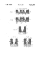
- FIGS. 1 through 5 are schematic representations of a portion of an MOS VLSI device at successive stages of a fabrication sequence that embodies the principles of the present invention.
- FIG. 1 A portion of an MOS VLSI device at an intermediate stage of its fabrication cycle is schematically represented in cross section in FIG. 1.
- the particular portion shown in FIG. 1 comprises a standard gate-and-source-and-drain (GASAD) structure known in the art.
- GASAD gate-and-source-and-drain
- the depicted structure comprises a silicon body 10 having conventional field-oxide (silicon dioxide) portions 12, 14 formed thereon.
- the vertical thickness t of the portions 12, 14 is approximately 4000-to-8000 Angstrom units ( ⁇ ).
- the lateral distance D between the facing walls of the portions 12, 14 is about 4-to-5 micrometers ( ⁇ m).
- the structure shown in FIG. 1 includes a gate-oxide (silicon dioxide) layer 16 that is about 175-to-350 ⁇ thick and a 2500-to-4000- ⁇ -thick doped polysilicon layer 18 that constitutes part of the gate of the MOS device.
- the structure also includes source and drain regions 20, 22 in the body 10.
- p-n junctions between the regions 20, 22 and the main portion of the body 10 are designated by dash lines.
- the depth of these junctions below the top surface of the body 10 is only approximately 1000-to-3000 ⁇ .
- FIG. 1 Also shown in FIG. 1 is a patterned layer of phosphorus-doped silicon dioxide comprising regions 24 through 27 each about 10,000 ⁇ thick. High-conductivity contacts and interconnects are intended to be made through openings formed in the phosphorus-doped silicon dioxide. In that way, electrical connections are made to the source and drain regions 20, 22 and to the doped polysilicon layer 18 of the depicted MOS device.
- the first step in forming electrical connections to the silicon and polysilicon surfaces of the FIG. 1 structure is to clean those surfaces and then to deposit thereon a film of titanium carbide. Cleaning is done, for example, by standard backsputter etching utilizing a pure argon atmosphere.
- the titanium carbide film is deposited by conventional reactive radio-frequency sputtering in an argon-methane gas mixture.
- the film is so deposited in a commercially available MRC 8667 horizontal magnetron system made by Materials Research Corporation, Orangeburg, N.Y.
- the titanium carbide deposited on the FIG. 1 structure is designed to be a titanium-rich film.
- a titanium-rich film will be designated herein as Ti x C, where x is the atomic ratio of titanium to carbon and 1 ⁇ x ⁇ 5-to-7.
- Different titanium-to-carbon ratios in the film are obtained by controlling deposition parameters such as power, pressure and the argon-to-methane ratio in the sputtering gas.
- a Ti x C film is sputter deposited on a surface in an argon-methane gas mixture in which the methane molar percentage in the mixture is in the range of about 0.1-to-6.
- the base pressure before the gases are introduced into the sputtering system is in the low 10 -7 Torr range and the total sputtering gas pressure is in the range of about 5-to-20 milliTorr.
- Total radio-frequency power in the system is maintained at about 200-to-800 watts, and the peak-to-peak voltages at the target and table of the system are established at about 200-to-400 and 10-to-50 volts, respectively.
- Ti x C films 150-to-1000 ⁇ thick are formed in, for example, 0.5-to-2minutes. (Of course, these parameters can vary from system to system and are to be taken only as specific examples of advantageous operating conditions in the specific aforeidentified system.)
- a titanium-rich film having a titanium-to-carbon ratio of about 3 is preferred.
- richer (i.e. x>3.1) formulations are also especially useful.
- values as high as 5 and in some instances as high as 7 are effective.
- an x value of 3.1 was found to be particularly advantageous for depositing the titanium-rich film on ⁇ 100> 20 ohm-centimeter p-type silicon.
- FIG. 3 is an enlargement of a limited portion of the FIG. 2 structure.
- FIG. 3 is an enlargement of only that portion that extends between reference lines 32, 33 of FIG. 2.
- FIGS. 3 through 5 will be utilized to describe subsequent steps in applicants' unique device fabrication sequence. But it is to be understood that the enlargements are representative of all portions of the device structure where a film of Ti x C is in contact with underlying silicon or polysilicon.
- the next step in applicants' fabrication sequence is to sinter or anneal the deposited Ti x C film 30 shown in FIG. 3.
- this step is carried out at a temperature in the range of 600-to-900 degrees Celsius for one-half-to-one hour in a vacuum (approximately 10 -6 Torr) or in an oxygen-free ambient such as argon, hydrogen, or nitrogen.
- a vacuum approximately 10 -6 Torr
- oxygen-free ambient such as argon, hydrogen, or nitrogen.
- annealing at 750 degrees Celsius for 30 minutes in 10 -6 Torr vacuum is advantageous.
- annealing of the Ti x C film 30 leads to phase separation in those portions of the film that directly overlie silicon or polysilicon.
- the portion of the film 30 that overlies the silicon region 20 is converted during annealing into a two-layer structure.
- the lower layer 32 of that structure comprises titanium silicide and the upper layer 34 comprises titanium carbide.
- the layer 32 of FIG. 4 results from the interaction of silicon of the body 10 with some of the titanium constituent of the originally deposited Ti x C layer.
- the layer 32 comprises TiSi 2 , an effective high-conductivity contact material.
- the upper layer 34 comprises Ti y C, where y ⁇ x.
- the layer 34 constitutes an effective barrier to aluminum diffusion. A reliable high-temperature-tolerant composite metallization for contacting silicon and for forming low-resistivity silicide-polysilicon gate-level interconnects is thereby provided.
- Portions of the originally deposited film 30 in contact with the phosphorus-doped silicon dioxide regions 24, 25 remain unaffected during the aforespecified annealing step.
- the constituency of these portions each designated by the reference numeral 30 in FIG. 4, remains Ti x C.
- the thickness of the TiSi 2 layer 32 (FIG. 4) was about 1000 ⁇ . In that case, the thickness of the overlying Ti y C layer 34 was approximately 250 ⁇ .
- a layer of aluminum about 0.7-to-1 ⁇ m thick is deposited over the entire top surface of the herein-considered MOS VLSI device structure.
- the aluminum layer and the underlying Ti x C film are then patterned to form portions in respective registry with specified underlying regions of the device structure.
- FIG. 5 shows one such patterned aluminum portion 36.
- the titanium carbide layer 34 is interposed as a barrier between the aluminum portion 36 and the silicide layer 32.
- a standard passivating layer (not shown) is typically deposited on the entire top surface of the device structure illustrated in FIG. 5.
- This layer comprises, for example, silicon nitride or trimethyl methoxy silane (TMMS).
- metallization systems useful for MOS VLSI devices and other applications of practical interest can be made in accordance with the principles of the present invention. These other systems involve the initial deposition of a film of titanium-rich titanium nitride, titanium-rich titanium boride, hafnium-rich hafnium carbide, hafnium-rich hafnium nitride, hafnium-rich hafnium boride, zirconium-rich zirconium carbide, zirconium-rich zirconium nitride, zirconium-rich zirconium boride, tantalum-rich tantalum carbide, tantalum-rich tantalum nitride, tantalum-rich tantalum boride, niobium-rich niobium carbide, niobium-rich niobium nitride or niobium-rich niobium boride.
- Standard processes are known in the art for forming such films.
- each of these films deposited on silicon or polysilicon undergoes a phase separation.
- a two-layer structure comprising a silicide (titanium silicide, hafnium silicide, zirconium silicide, tantalum silicide or niobium silicide) and an overlying diffusion barrier (titanium nitride, titanium boride, hafnium carbide, hafnium nitride, hafnium boride, zirconium carbide, zirconium nitride, zirconium boride, tantalum carbide, tantalum nitride, tantalum boride, niobium carbide, niobium nitride or niobium boride) is formed in a single processing step.
Landscapes
- Electrodes Of Semiconductors (AREA)
Priority Applications (3)
| Application Number | Priority Date | Filing Date | Title |
|---|---|---|---|
| US06/528,074 US4502209A (en) | 1983-08-31 | 1983-08-31 | Forming low-resistance contact to silicon |
| CA000441088A CA1200155A (en) | 1983-08-31 | 1983-11-14 | Forming low-resistance contact to silicon |
| JP58225547A JPS6060720A (ja) | 1983-08-31 | 1983-12-01 | 半導体デバイス作成方法 |
Applications Claiming Priority (1)
| Application Number | Priority Date | Filing Date | Title |
|---|---|---|---|
| US06/528,074 US4502209A (en) | 1983-08-31 | 1983-08-31 | Forming low-resistance contact to silicon |
Publications (1)
| Publication Number | Publication Date |
|---|---|
| US4502209A true US4502209A (en) | 1985-03-05 |
Family
ID=24104162
Family Applications (1)
| Application Number | Title | Priority Date | Filing Date |
|---|---|---|---|
| US06/528,074 Expired - Lifetime US4502209A (en) | 1983-08-31 | 1983-08-31 | Forming low-resistance contact to silicon |
Country Status (3)
| Country | Link |
|---|---|
| US (1) | US4502209A (ja) |
| JP (1) | JPS6060720A (ja) |
| CA (1) | CA1200155A (ja) |
Cited By (52)
| Publication number | Priority date | Publication date | Assignee | Title |
|---|---|---|---|---|
| JPS61226959A (ja) * | 1985-03-30 | 1986-10-08 | Toshiba Corp | 半導体装置およびその製造方法 |
| US4738937A (en) * | 1985-10-22 | 1988-04-19 | Hughes Aircraft Company | Method of making ohmic contact structure |
| EP0223013A3 (en) * | 1985-11-18 | 1988-05-04 | International Business Machines Corporation | Planar 3d epitaxial semiconductor structures and method for making |
| US4804636A (en) * | 1985-05-01 | 1989-02-14 | Texas Instruments Incorporated | Process for making integrated circuits having titanium nitride triple interconnect |
| US4811078A (en) * | 1985-05-01 | 1989-03-07 | Texas Instruments Incorporated | Integrated circuit device and process with tin capacitors |
| US4811076A (en) * | 1985-05-01 | 1989-03-07 | Texas Instruments Incorporated | Device and process with doubled capacitors |
| US4814854A (en) * | 1985-05-01 | 1989-03-21 | Texas Instruments Incorporated | Integrated circuit device and process with tin-gate transistor |
| US4821085A (en) * | 1985-05-01 | 1989-04-11 | Texas Instruments Incorporated | VLSI local interconnect structure |
| US4823182A (en) * | 1986-11-21 | 1989-04-18 | Kabushiki Kaisha Toshiba | Semiconductor device with a diffusion barrier contact of a refractory metal nitride and either carbon or boron |
| US4843453A (en) * | 1985-05-10 | 1989-06-27 | Texas Instruments Incorporated | Metal contacts and interconnections for VLSI devices |
| US4890141A (en) * | 1985-05-01 | 1989-12-26 | Texas Instruments Incorporated | CMOS device with both p+ and n+ gates |
| US4894693A (en) * | 1985-05-01 | 1990-01-16 | Tigelaar Howard L | Single-polysilicon dram device and process |
| US4920071A (en) * | 1985-03-15 | 1990-04-24 | Fairchild Camera And Instrument Corporation | High temperature interconnect system for an integrated circuit |
| US4962414A (en) * | 1988-02-11 | 1990-10-09 | Sgs-Thomson Microelectronics, Inc. | Method for forming a contact VIA |
| US4975756A (en) * | 1985-05-01 | 1990-12-04 | Texas Instruments Incorporated | SRAM with local interconnect |
| US5039578A (en) * | 1986-06-24 | 1991-08-13 | At&T Bell Laboratories | Method for fabricating devices in III-V semiconductor substrates and devices formed thereby |
| US5063422A (en) * | 1988-06-20 | 1991-11-05 | At&T Bell Laboratories | Devices having shallow junctions |
| US5084416A (en) * | 1989-02-17 | 1992-01-28 | Matsushita Electronics Corporation | Method of forming a low resistance contact by forming a contact hole within a recess |
| US5087578A (en) * | 1986-09-26 | 1992-02-11 | Kabushiki Kaisha Toshiba | Semiconductor device having multi-layered wiring |
| US5102827A (en) * | 1989-05-31 | 1992-04-07 | At&T Bell Laboratories | Contact metallization of semiconductor integrated-circuit devices |
| US5132756A (en) * | 1988-01-14 | 1992-07-21 | Kabushiki Kaisha Toshiba | Method of manufacturing semiconductor devices |
| US5278099A (en) * | 1985-05-13 | 1994-01-11 | Kabushiki Kaisha Toshiba | Method for manufacturing a semiconductor device having wiring electrodes |
| US5369302A (en) * | 1990-10-22 | 1994-11-29 | Sgs-Thomson Microelectronics, Inc. | Method to improve step coverage by contact reflow |
| US5374592A (en) * | 1992-09-22 | 1994-12-20 | Sgs-Thomson Microelectronics, Inc. | Method for forming an aluminum metal contact |
| US5472912A (en) * | 1989-11-30 | 1995-12-05 | Sgs-Thomson Microelectronics, Inc. | Method of making an integrated circuit structure by using a non-conductive plug |
| US5525837A (en) * | 1995-01-26 | 1996-06-11 | Lsi Logic Corporation | Reliable metallization with barrier for semiconductors |
| US5594269A (en) * | 1991-08-06 | 1997-01-14 | Sgs-Thomson Microelectronics, Inc. | Resistive load for integrated circuit devices |
| US5596221A (en) * | 1994-09-29 | 1997-01-21 | Mitsubishi Denki Kabushiki Kaisha | Bipolar transistor with emitter double contact structure |
| US5625231A (en) * | 1995-03-10 | 1997-04-29 | Advanced Micro Devices, Inc. | Low cost solution to high aspect ratio contact/via adhesion layer application for deep sub-half micrometer back-end-of line technology |
| US5658828A (en) * | 1989-11-30 | 1997-08-19 | Sgs-Thomson Microelectronics, Inc. | Method for forming an aluminum contact through an insulating layer |
| US5930673A (en) * | 1990-11-05 | 1999-07-27 | Stmicroelectronics, Inc. | Method for forming a metal contact |
| US5956612A (en) * | 1996-08-09 | 1999-09-21 | Micron Technology, Inc. | Trench/hole fill processes for semiconductor fabrication |
| US5998825A (en) * | 1996-10-18 | 1999-12-07 | Sony Corporation | Capacitor structure of semiconductor memory cell and method for fabricating capacitor structure of semiconductor memory cell |
| US6077775A (en) * | 1998-08-20 | 2000-06-20 | The United States Of America As Represented By The Secretary Of The Navy | Process for making a semiconductor device with barrier film formation using a metal halide and products thereof |
| US6083818A (en) * | 1998-08-20 | 2000-07-04 | The United States Of America As Represented By The Secretary Of The Navy | Electronic devices with strontium barrier film and process for making same |
| US6127276A (en) * | 1998-06-02 | 2000-10-03 | United Microelectronics Corp | Method of formation for a via opening |
| US6156644A (en) * | 1995-12-07 | 2000-12-05 | Samsung Electronics Co., Ltd. | Method for forming interconnects for semiconductor devices using reaction control layers, and interconnects formed thereby |
| US6171953B1 (en) | 1998-08-20 | 2001-01-09 | The United States Of America As Represented By The Secretary Of The Navy | Processes for making electronic devices with rubidum barrier film |
| US6235630B1 (en) * | 1998-08-19 | 2001-05-22 | Micron Technology, Inc. | Silicide pattern structures and methods of fabricating the same |
| SG80582A1 (en) * | 1997-03-20 | 2001-05-22 | Chartered Semiconductor Mfg | Use of an insulator spacer on the sidewalls of a via hole |
| US6242811B1 (en) | 1989-11-30 | 2001-06-05 | Stmicroelectronics, Inc. | Interlevel contact including aluminum-refractory metal alloy formed during aluminum deposition at an elevated temperature |
| US6271137B1 (en) * | 1989-11-30 | 2001-08-07 | Stmicroelectronics, Inc. | Method of producing an aluminum stacked contact/via for multilayer |
| US6287963B1 (en) | 1990-11-05 | 2001-09-11 | Stmicroelectronics, Inc. | Method for forming a metal contact |
| US6291876B1 (en) | 1998-08-20 | 2001-09-18 | The United States Of America As Represented By The Secretary Of The Navy | Electronic devices with composite atomic barrier film and process for making same |
| US6351036B1 (en) | 1998-08-20 | 2002-02-26 | The United States Of America As Represented By The Secretary Of The Navy | Electronic devices with a barrier film and process for making same |
| US6614082B1 (en) * | 1999-01-29 | 2003-09-02 | Micron Technology, Inc. | Fabrication of semiconductor devices with transition metal boride films as diffusion barriers |
| US6617242B1 (en) | 1989-11-30 | 2003-09-09 | Stmicroelectronics, Inc. | Method for fabricating interlevel contacts of aluminum/refractory metal alloys |
| US6690044B1 (en) * | 1993-03-19 | 2004-02-10 | Micron Technology, Inc. | Approach to avoid buckling BPSG by using an intermediate barrier layer |
| US6720654B2 (en) | 1998-08-20 | 2004-04-13 | The United States Of America As Represented By The Secretary Of The Navy | Electronic devices with cesium barrier film and process for making same |
| US6734558B2 (en) | 1998-08-20 | 2004-05-11 | The United States Of America As Represented By The Secretary Of The Navy | Electronic devices with barium barrier film and process for making same |
| US20080251928A1 (en) * | 2007-04-11 | 2008-10-16 | Hui-Lin Chang | Carbonization of metal caps |
| US20140246734A1 (en) * | 2013-03-01 | 2014-09-04 | Globalfoundries Inc. | Replacement metal gate with mulitiple titanium nitride laters |
Families Citing this family (1)
| Publication number | Priority date | Publication date | Assignee | Title |
|---|---|---|---|---|
| JPH0824112B2 (ja) * | 1993-02-17 | 1996-03-06 | 日本電気株式会社 | 半導体装置およびその製造方法 |
Citations (3)
| Publication number | Priority date | Publication date | Assignee | Title |
|---|---|---|---|---|
| US3714520A (en) * | 1970-12-15 | 1973-01-30 | Gen Electric | High temperature low ohmic contact to silicon |
| US3794516A (en) * | 1970-12-15 | 1974-02-26 | W Engeler | Method for making high temperature low ohmic contact to silicon |
| US3879746A (en) * | 1972-05-30 | 1975-04-22 | Bell Telephone Labor Inc | Gate metallization structure |
-
1983
- 1983-08-31 US US06/528,074 patent/US4502209A/en not_active Expired - Lifetime
- 1983-11-14 CA CA000441088A patent/CA1200155A/en not_active Expired
- 1983-12-01 JP JP58225547A patent/JPS6060720A/ja active Granted
Patent Citations (3)
| Publication number | Priority date | Publication date | Assignee | Title |
|---|---|---|---|---|
| US3714520A (en) * | 1970-12-15 | 1973-01-30 | Gen Electric | High temperature low ohmic contact to silicon |
| US3794516A (en) * | 1970-12-15 | 1974-02-26 | W Engeler | Method for making high temperature low ohmic contact to silicon |
| US3879746A (en) * | 1972-05-30 | 1975-04-22 | Bell Telephone Labor Inc | Gate metallization structure |
Non-Patent Citations (2)
| Title |
|---|
| "Interaction of Reactively Sputtered Titanium Carbide Thin Films with Si, SiO2 Ti, TiSi2, and Al", J. Appl. Phys., 54(6), Jun. 1983, M. Eizenberg et al, pp. 3195-3199. |
| Interaction of Reactively Sputtered Titanium Carbide Thin Films with Si, SiO 2 Ti, TiSi 2 , and Al , J. Appl. Phys., 54(6), Jun. 1983, M. Eizenberg et al, pp. 3195 3199. * |
Cited By (75)
| Publication number | Priority date | Publication date | Assignee | Title |
|---|---|---|---|---|
| US4920071A (en) * | 1985-03-15 | 1990-04-24 | Fairchild Camera And Instrument Corporation | High temperature interconnect system for an integrated circuit |
| US5414301A (en) * | 1985-03-15 | 1995-05-09 | National Semiconductor Corporation | High temperature interconnect system for an integrated circuit |
| JP2577342B2 (ja) | 1985-03-30 | 1997-01-29 | 株式会社東芝 | 半導体装置およびその製造方法 |
| JPS61226959A (ja) * | 1985-03-30 | 1986-10-08 | Toshiba Corp | 半導体装置およびその製造方法 |
| US4890141A (en) * | 1985-05-01 | 1989-12-26 | Texas Instruments Incorporated | CMOS device with both p+ and n+ gates |
| US4804636A (en) * | 1985-05-01 | 1989-02-14 | Texas Instruments Incorporated | Process for making integrated circuits having titanium nitride triple interconnect |
| US4814854A (en) * | 1985-05-01 | 1989-03-21 | Texas Instruments Incorporated | Integrated circuit device and process with tin-gate transistor |
| US4821085A (en) * | 1985-05-01 | 1989-04-11 | Texas Instruments Incorporated | VLSI local interconnect structure |
| US5302539A (en) * | 1985-05-01 | 1994-04-12 | Texas Instruments Incorporated | VLSI interconnect method and structure |
| US4894693A (en) * | 1985-05-01 | 1990-01-16 | Tigelaar Howard L | Single-polysilicon dram device and process |
| US4811078A (en) * | 1985-05-01 | 1989-03-07 | Texas Instruments Incorporated | Integrated circuit device and process with tin capacitors |
| US4975756A (en) * | 1985-05-01 | 1990-12-04 | Texas Instruments Incorporated | SRAM with local interconnect |
| US4811076A (en) * | 1985-05-01 | 1989-03-07 | Texas Instruments Incorporated | Device and process with doubled capacitors |
| US4843453A (en) * | 1985-05-10 | 1989-06-27 | Texas Instruments Incorporated | Metal contacts and interconnections for VLSI devices |
| US5278099A (en) * | 1985-05-13 | 1994-01-11 | Kabushiki Kaisha Toshiba | Method for manufacturing a semiconductor device having wiring electrodes |
| US4738937A (en) * | 1985-10-22 | 1988-04-19 | Hughes Aircraft Company | Method of making ohmic contact structure |
| EP0223013A3 (en) * | 1985-11-18 | 1988-05-04 | International Business Machines Corporation | Planar 3d epitaxial semiconductor structures and method for making |
| US5039578A (en) * | 1986-06-24 | 1991-08-13 | At&T Bell Laboratories | Method for fabricating devices in III-V semiconductor substrates and devices formed thereby |
| US5087578A (en) * | 1986-09-26 | 1992-02-11 | Kabushiki Kaisha Toshiba | Semiconductor device having multi-layered wiring |
| US4823182A (en) * | 1986-11-21 | 1989-04-18 | Kabushiki Kaisha Toshiba | Semiconductor device with a diffusion barrier contact of a refractory metal nitride and either carbon or boron |
| US5132756A (en) * | 1988-01-14 | 1992-07-21 | Kabushiki Kaisha Toshiba | Method of manufacturing semiconductor devices |
| US4962414A (en) * | 1988-02-11 | 1990-10-09 | Sgs-Thomson Microelectronics, Inc. | Method for forming a contact VIA |
| US5063422A (en) * | 1988-06-20 | 1991-11-05 | At&T Bell Laboratories | Devices having shallow junctions |
| US5084416A (en) * | 1989-02-17 | 1992-01-28 | Matsushita Electronics Corporation | Method of forming a low resistance contact by forming a contact hole within a recess |
| EP0383610B1 (en) * | 1989-02-17 | 1997-10-08 | Matsushita Electronics Corporation | Manufacturing method of semiconductor device |
| US5102827A (en) * | 1989-05-31 | 1992-04-07 | At&T Bell Laboratories | Contact metallization of semiconductor integrated-circuit devices |
| US6617242B1 (en) | 1989-11-30 | 2003-09-09 | Stmicroelectronics, Inc. | Method for fabricating interlevel contacts of aluminum/refractory metal alloys |
| US5472912A (en) * | 1989-11-30 | 1995-12-05 | Sgs-Thomson Microelectronics, Inc. | Method of making an integrated circuit structure by using a non-conductive plug |
| US6271137B1 (en) * | 1989-11-30 | 2001-08-07 | Stmicroelectronics, Inc. | Method of producing an aluminum stacked contact/via for multilayer |
| US6242811B1 (en) | 1989-11-30 | 2001-06-05 | Stmicroelectronics, Inc. | Interlevel contact including aluminum-refractory metal alloy formed during aluminum deposition at an elevated temperature |
| US5976969A (en) * | 1989-11-30 | 1999-11-02 | Stmicroelectronics, Inc. | Method for forming an aluminum contact |
| US5658828A (en) * | 1989-11-30 | 1997-08-19 | Sgs-Thomson Microelectronics, Inc. | Method for forming an aluminum contact through an insulating layer |
| US5369302A (en) * | 1990-10-22 | 1994-11-29 | Sgs-Thomson Microelectronics, Inc. | Method to improve step coverage by contact reflow |
| US5930673A (en) * | 1990-11-05 | 1999-07-27 | Stmicroelectronics, Inc. | Method for forming a metal contact |
| US6287963B1 (en) | 1990-11-05 | 2001-09-11 | Stmicroelectronics, Inc. | Method for forming a metal contact |
| US5594269A (en) * | 1991-08-06 | 1997-01-14 | Sgs-Thomson Microelectronics, Inc. | Resistive load for integrated circuit devices |
| US5374592A (en) * | 1992-09-22 | 1994-12-20 | Sgs-Thomson Microelectronics, Inc. | Method for forming an aluminum metal contact |
| US6690044B1 (en) * | 1993-03-19 | 2004-02-10 | Micron Technology, Inc. | Approach to avoid buckling BPSG by using an intermediate barrier layer |
| US7485961B2 (en) | 1993-03-19 | 2009-02-03 | Micron Technology, Inc. | Approach to avoid buckling in BPSG by using an intermediate barrier layer |
| US20040188840A1 (en) * | 1993-03-19 | 2004-09-30 | Doan Trung T. | Approach to avoid buckling in BPSG by using an intermediate barrier layer |
| US6433435B2 (en) | 1993-11-30 | 2002-08-13 | Stmicroelectronics, Inc. | Aluminum contact structure for integrated circuits |
| US5596221A (en) * | 1994-09-29 | 1997-01-21 | Mitsubishi Denki Kabushiki Kaisha | Bipolar transistor with emitter double contact structure |
| US5614437A (en) * | 1995-01-26 | 1997-03-25 | Lsi Logic Corporation | Method for fabricating reliable metallization with Ta-Si-N barrier for semiconductors |
| US5525837A (en) * | 1995-01-26 | 1996-06-11 | Lsi Logic Corporation | Reliable metallization with barrier for semiconductors |
| US5625231A (en) * | 1995-03-10 | 1997-04-29 | Advanced Micro Devices, Inc. | Low cost solution to high aspect ratio contact/via adhesion layer application for deep sub-half micrometer back-end-of line technology |
| US6156644A (en) * | 1995-12-07 | 2000-12-05 | Samsung Electronics Co., Ltd. | Method for forming interconnects for semiconductor devices using reaction control layers, and interconnects formed thereby |
| US5956612A (en) * | 1996-08-09 | 1999-09-21 | Micron Technology, Inc. | Trench/hole fill processes for semiconductor fabrication |
| US5998825A (en) * | 1996-10-18 | 1999-12-07 | Sony Corporation | Capacitor structure of semiconductor memory cell and method for fabricating capacitor structure of semiconductor memory cell |
| US6287934B1 (en) | 1996-10-18 | 2001-09-11 | Sony Corporation | Capacitor structure of semiconductor memory cell and method for fabricating capacitor structure of semiconductor cell |
| SG80582A1 (en) * | 1997-03-20 | 2001-05-22 | Chartered Semiconductor Mfg | Use of an insulator spacer on the sidewalls of a via hole |
| US6127276A (en) * | 1998-06-02 | 2000-10-03 | United Microelectronics Corp | Method of formation for a via opening |
| US6716745B2 (en) | 1998-08-19 | 2004-04-06 | Micron Technology, Iinc. | Silicide pattern structures and methods of fabricating the same |
| US20040038511A1 (en) * | 1998-08-19 | 2004-02-26 | Salman Akram | Methods of fabricating silicide pattern structures |
| US20050136647A1 (en) * | 1998-08-19 | 2005-06-23 | Salman Akram | Methods of fabricating contact interfaces |
| US6410420B2 (en) | 1998-08-19 | 2002-06-25 | Micron Technology, Inc. | Method of fabricating silicide pattern structures |
| US6235630B1 (en) * | 1998-08-19 | 2001-05-22 | Micron Technology, Inc. | Silicide pattern structures and methods of fabricating the same |
| US6881663B2 (en) | 1998-08-19 | 2005-04-19 | Micron Technology, Inc. | Methods of fabricating silicide pattern structures |
| US6599832B2 (en) | 1998-08-19 | 2003-07-29 | Micron Technology, Inc. | Silicide pattern structures and methods of fabricating the same |
| US6171953B1 (en) | 1998-08-20 | 2001-01-09 | The United States Of America As Represented By The Secretary Of The Navy | Processes for making electronic devices with rubidum barrier film |
| US6566247B2 (en) | 1998-08-20 | 2003-05-20 | The United States Of America As Represented By The Secretary Of The Navy | Electronic devices with composite atomic barrier film and process for making same |
| US6188134B1 (en) | 1998-08-20 | 2001-02-13 | The United States Of America As Represented By The Secretary Of The Navy | Electronic devices with rubidium barrier film and process for making same |
| US6077775A (en) * | 1998-08-20 | 2000-06-20 | The United States Of America As Represented By The Secretary Of The Navy | Process for making a semiconductor device with barrier film formation using a metal halide and products thereof |
| US6291876B1 (en) | 1998-08-20 | 2001-09-18 | The United States Of America As Represented By The Secretary Of The Navy | Electronic devices with composite atomic barrier film and process for making same |
| US6351036B1 (en) | 1998-08-20 | 2002-02-26 | The United States Of America As Represented By The Secretary Of The Navy | Electronic devices with a barrier film and process for making same |
| US6144050A (en) * | 1998-08-20 | 2000-11-07 | The United States Of America As Represented By The Secretary Of The Navy | Electronic devices with strontium barrier film and process for making same |
| US6720654B2 (en) | 1998-08-20 | 2004-04-13 | The United States Of America As Represented By The Secretary Of The Navy | Electronic devices with cesium barrier film and process for making same |
| US6734558B2 (en) | 1998-08-20 | 2004-05-11 | The United States Of America As Represented By The Secretary Of The Navy | Electronic devices with barium barrier film and process for making same |
| US6083818A (en) * | 1998-08-20 | 2000-07-04 | The United States Of America As Represented By The Secretary Of The Navy | Electronic devices with strontium barrier film and process for making same |
| US6614082B1 (en) * | 1999-01-29 | 2003-09-02 | Micron Technology, Inc. | Fabrication of semiconductor devices with transition metal boride films as diffusion barriers |
| US6872639B2 (en) | 1999-01-29 | 2005-03-29 | Micron Technology, Inc. | Fabrication of semiconductor devices with transition metal boride films as diffusion barriers |
| US6613654B1 (en) | 1999-01-29 | 2003-09-02 | Micron Technology Inc | Fabrication of semiconductor devices with transition metal boride films as diffusion barriers |
| US20030203608A1 (en) * | 1999-01-29 | 2003-10-30 | Deboer Scott J. | Fabrication of semiconductor devices with transition metal boride films as diffusion barriers |
| US20080251928A1 (en) * | 2007-04-11 | 2008-10-16 | Hui-Lin Chang | Carbonization of metal caps |
| US9385034B2 (en) * | 2007-04-11 | 2016-07-05 | Taiwan Semiconductor Manufacturing Company, Ltd. | Carbonization of metal caps |
| US20140246734A1 (en) * | 2013-03-01 | 2014-09-04 | Globalfoundries Inc. | Replacement metal gate with mulitiple titanium nitride laters |
Also Published As
| Publication number | Publication date |
|---|---|
| JPS6060720A (ja) | 1985-04-08 |
| CA1200155A (en) | 1986-02-04 |
| JPH0365655B2 (ja) | 1991-10-14 |
Similar Documents
| Publication | Publication Date | Title |
|---|---|---|
| CA1200155A (en) | Forming low-resistance contact to silicon | |
| US5242860A (en) | Method for the formation of tin barrier layer with preferential (111) crystallographic orientation | |
| US5893752A (en) | Process for forming a semiconductor device | |
| US6054382A (en) | Method of improving texture of metal films in semiconductor integrated circuits | |
| JPH0653163A (ja) | 集積回路障壁構造体とその製法 | |
| JPH05315284A (ja) | コンタクト部形成方法 | |
| CA1241457A (en) | Integrated devices having titanium carbonitride diffusion barrier layer | |
| US5366928A (en) | Method of manufacturing a semiconductor device, in which a metal conductor track is provided on a surface of a semiconductor body | |
| JPS61133646A (ja) | 半導体装置の製造方法 | |
| JP3252397B2 (ja) | 配線形成方法 | |
| US5528081A (en) | High temperature refractory metal contact in silicon integrated circuits | |
| US7199040B2 (en) | Barrier layer structure | |
| JP3361971B2 (ja) | 窒化金属変換方法および半導体装置の製造方法 | |
| US5350711A (en) | Method of fabricating high temperature refractory metal nitride contact and interconnect structure | |
| CN115084004A (zh) | 制造半导体结构的方法及半导体结构 | |
| US4839715A (en) | Chip contacts without oxide discontinuities | |
| EP0225224A2 (en) | After oxide metal alloy process | |
| JPH07130849A (ja) | 半導体装置及びその製造方法 | |
| KR19980033882A (ko) | 반도체 디바이스의 금속 배선 형성 방법 | |
| JP3119505B2 (ja) | 半導体装置 | |
| JP2803676B2 (ja) | 半導体装置の製造方法 | |
| JPH04324636A (ja) | 半導体装置およびその製造方法 | |
| JPH05129223A (ja) | 半導体装置の製造方法 | |
| KR100342826B1 (ko) | 반도체소자의베리어금속층형성방법 | |
| JPH04290425A (ja) | 耐熱性配線の形成方法 |
Legal Events
| Date | Code | Title | Description |
|---|---|---|---|
| AS | Assignment |
Owner name: BELL TELEPHONE LABORATORIES, INCORPORATED 600 MOUN Free format text: ASSIGNMENT OF ASSIGNORS INTEREST.;ASSIGNORS:EIZENBERG, MOSHE;MURARKA, SHYAM P.;REEL/FRAME:004170/0163 Effective date: 19830826 |
|
| STCF | Information on status: patent grant |
Free format text: PATENTED CASE |
|
| FEPP | Fee payment procedure |
Free format text: PAYOR NUMBER ASSIGNED (ORIGINAL EVENT CODE: ASPN); ENTITY STATUS OF PATENT OWNER: LARGE ENTITY |
|
| FPAY | Fee payment |
Year of fee payment: 4 |
|
| FPAY | Fee payment |
Year of fee payment: 8 |
|
| FPAY | Fee payment |
Year of fee payment: 12 |