US4179326A - Process for the vapor growth of a thin film - Google Patents
Process for the vapor growth of a thin film Download PDFInfo
- Publication number
- US4179326A US4179326A US05/787,495 US78749577A US4179326A US 4179326 A US4179326 A US 4179326A US 78749577 A US78749577 A US 78749577A US 4179326 A US4179326 A US 4179326A
- Authority
- US
- United States
- Prior art keywords
- wafers
- constant
- reaction tube
- process according
- reaction
- Prior art date
- Legal status (The legal status is an assumption and is not a legal conclusion. Google has not performed a legal analysis and makes no representation as to the accuracy of the status listed.)
- Expired - Lifetime
Links
Images


Classifications
-
- C—CHEMISTRY; METALLURGY
- C23—COATING METALLIC MATERIAL; COATING MATERIAL WITH METALLIC MATERIAL; CHEMICAL SURFACE TREATMENT; DIFFUSION TREATMENT OF METALLIC MATERIAL; COATING BY VACUUM EVAPORATION, BY SPUTTERING, BY ION IMPLANTATION OR BY CHEMICAL VAPOUR DEPOSITION, IN GENERAL; INHIBITING CORROSION OF METALLIC MATERIAL OR INCRUSTATION IN GENERAL
- C23C—COATING METALLIC MATERIAL; COATING MATERIAL WITH METALLIC MATERIAL; SURFACE TREATMENT OF METALLIC MATERIAL BY DIFFUSION INTO THE SURFACE, BY CHEMICAL CONVERSION OR SUBSTITUTION; COATING BY VACUUM EVAPORATION, BY SPUTTERING, BY ION IMPLANTATION OR BY CHEMICAL VAPOUR DEPOSITION, IN GENERAL
- C23C16/00—Chemical coating by decomposition of gaseous compounds, without leaving reaction products of surface material in the coating, i.e. chemical vapour deposition [CVD] processes
- C23C16/44—Chemical coating by decomposition of gaseous compounds, without leaving reaction products of surface material in the coating, i.e. chemical vapour deposition [CVD] processes characterised by the method of coating
- C23C16/458—Chemical coating by decomposition of gaseous compounds, without leaving reaction products of surface material in the coating, i.e. chemical vapour deposition [CVD] processes characterised by the method of coating characterised by the method used for supporting substrates in the reaction chamber
-
- C—CHEMISTRY; METALLURGY
- C30—CRYSTAL GROWTH
- C30B—SINGLE-CRYSTAL GROWTH; UNIDIRECTIONAL SOLIDIFICATION OF EUTECTIC MATERIAL OR UNIDIRECTIONAL DEMIXING OF EUTECTOID MATERIAL; REFINING BY ZONE-MELTING OF MATERIAL; PRODUCTION OF A HOMOGENEOUS POLYCRYSTALLINE MATERIAL WITH DEFINED STRUCTURE; SINGLE CRYSTALS OR HOMOGENEOUS POLYCRYSTALLINE MATERIAL WITH DEFINED STRUCTURE; AFTER-TREATMENT OF SINGLE CRYSTALS OR A HOMOGENEOUS POLYCRYSTALLINE MATERIAL WITH DEFINED STRUCTURE; APPARATUS THEREFOR
- C30B25/00—Single-crystal growth by chemical reaction of reactive gases, e.g. chemical vapour-deposition growth
- C30B25/02—Epitaxial-layer growth
- C30B25/14—Feed and outlet means for the gases; Modifying the flow of the reactive gases
-
- Y—GENERAL TAGGING OF NEW TECHNOLOGICAL DEVELOPMENTS; GENERAL TAGGING OF CROSS-SECTIONAL TECHNOLOGIES SPANNING OVER SEVERAL SECTIONS OF THE IPC; TECHNICAL SUBJECTS COVERED BY FORMER USPC CROSS-REFERENCE ART COLLECTIONS [XRACs] AND DIGESTS
- Y10—TECHNICAL SUBJECTS COVERED BY FORMER USPC
- Y10S—TECHNICAL SUBJECTS COVERED BY FORMER USPC CROSS-REFERENCE ART COLLECTIONS [XRACs] AND DIGESTS
- Y10S148/00—Metal treatment
- Y10S148/006—Apparatus
-
- Y—GENERAL TAGGING OF NEW TECHNOLOGICAL DEVELOPMENTS; GENERAL TAGGING OF CROSS-SECTIONAL TECHNOLOGIES SPANNING OVER SEVERAL SECTIONS OF THE IPC; TECHNICAL SUBJECTS COVERED BY FORMER USPC CROSS-REFERENCE ART COLLECTIONS [XRACs] AND DIGESTS
- Y10—TECHNICAL SUBJECTS COVERED BY FORMER USPC
- Y10S—TECHNICAL SUBJECTS COVERED BY FORMER USPC CROSS-REFERENCE ART COLLECTIONS [XRACs] AND DIGESTS
- Y10S148/00—Metal treatment
- Y10S148/118—Oxide films
-
- Y—GENERAL TAGGING OF NEW TECHNOLOGICAL DEVELOPMENTS; GENERAL TAGGING OF CROSS-SECTIONAL TECHNOLOGIES SPANNING OVER SEVERAL SECTIONS OF THE IPC; TECHNICAL SUBJECTS COVERED BY FORMER USPC CROSS-REFERENCE ART COLLECTIONS [XRACs] AND DIGESTS
- Y10—TECHNICAL SUBJECTS COVERED BY FORMER USPC
- Y10S—TECHNICAL SUBJECTS COVERED BY FORMER USPC CROSS-REFERENCE ART COLLECTIONS [XRACs] AND DIGESTS
- Y10S148/00—Metal treatment
- Y10S148/125—Polycrystalline passivation
Definitions
- the present invention relates to a process for the vapor growth of a thin film and, more particularly, to a process for the vapor growth of a thin film having a uniform thickness on a plurality of wafers.
- the vapor growth technique is widely employed for growing a thin semiconductive, conductive or insulating film, on a substrate or wafer.
- the wafer is used for the manufacture of semiconductor devices referred to as IC, LSI and the like.
- a reaction gas are caused to flow through a reaction tube under normal or reduced pressure and brought into contact with the wafers arranged in the reaction tube.
- the vapor growth process is widely performed under a reduced pressure, for example, 10 Torr.
- a reduced pressure for example, 10 Torr.
- a plurality of wafers can be simultaneously treated in the reaction tube which usually has a circular cross-sectional space therein.
- the conventional vapor growth process under a reduced pressure is, however, disadvantageous in that the thickness of a film grown on one piece of wafer by such process can occasionally be nonuniform.
- the subsequent processes for treating the wafer such as etching of the thin film, may become very complicated in order to produce a uniformly thick film all over the wafer after completion of such treating processes.
- the Inventors devoted themselves to the investigation of the vapor growths of thin films, and discovered that the thickness distribution of the film over one piece of wafer is greatly influenced by the location of the wafers in the reaction tube. In addition, the Inventors discovered that the optimum location of the wafers should be changed in accordance with the specific pressure within the reaction tube.
- the wafers are arranged in parallel to each other and in the flow direction of a predetermined reaction gas flowing through the reaction tube, with the wafers arranged almost perpendicularly to the above-mentioned flow direction.
- This is improved by a particular feature of the present invention.
- This particular feature essentially requires that the wafers be arranged concentrically to the axis of the reaction tube, and further that the vapor growth be performed under a condition which satisfies the formula:
- H denotes a distance (in mm) between two adjacent exposed surfaces of the wafers
- W denotes a width (in mm) between the inner wall of the reaction tube and the peripheral edge of each of the wafers
- P denotes an average value of the reduced pressure which varies from less than 1.2 to 5.0 Torr
- a denotes a constant of 0.8 Torr -1
- b denotes a constant of from 0.3 to 1.2 which is determined by the predetermined reaction gas.
- the vapor growth is performed according to another feature of the invention and under a condition which satisfies the formula:
- the vapor growth process therefore, comprises the steps of: supporting a plurality of wafer pieces at a part or a few parts of the peripheral edge of each of the wafers; arranging the wafers in a reaction tube along the flowing direction of a reaction gas therein; forming a clearance between the inner wall of the reaction tube and the other unsupported parts of the peripheral edge of each piece of wafer; flowing the reaction gas through the reaction tube via the above-mentioned clearance; heating the wafers to a required temperature for depositing the film on the wafers; maintaining a pressure within the reaction tube at a predetermined reduced value.
- the inner wall of the reaction tube defines a reaction chamber usually exhibiting a circular cross section, as wafers are generally available in round disc form either with or without a flat portion around a part of the edge.
- a reaction tube which has a shape similar to the wafer even when the wafer is not in the form of a disc.
- the wafer can consist of a semiconductive material, such as Si, Ge and GaAs and the like, or an insulating material, such as Al 2 O 3 and the like.
- the wafer can also include a body of a material having various layers thereon, such as insulating and active layers.
- the number of wafers treated at a time is generally from 30 to 100 pieces, and preferably more than 40 pieces.
- the wafer can have a diameter of 75 mm or less or even a diameter of 125 mm or less.
- W and H can be equal to any value when they satisfy one of the two equations (1) and (2); but the value of W should preferably be from 4 to 20 mm, and the value of H should preferably be from 8 to 40 mm, respectively.
- the constant "b” of the formula (1) varies from 0.3 to 1.2 depending upon the kind of reaction gas. It was discovered by the Inventors that the preferably value of the constant "b” is mainly influenced by the molecular weight of the reaction gas or by the sum of the molecular weights of the reaction gases as listed below.
- the term "molecular weight of the reaction gas” is used below to include "sum of the molecular weights of the reaction gases”.
- the constant "b" should preferably be approximately one hundredth of the molecular weight of the gas which is required in the formation of the film during the vapor growth reaction, when this molecular weight does not exceed 100.
- the constant "b" should be determined, depending upon the different kinds of reaction gas, in the following ways.
- the ratio of H/W is determined by the formula (2), this ratio should be varied between the maximum value of 2 and the minimum value of a ⁇ P+0.3, depending upon the kind of the reaction gas.
- the ratio H/W equals the minimum value.
- the equation determining the ratio H/W can be expressed by the formula:
- the constant "c” decreases from 0.8 to 0 and the constant "d” increases from 0.3 to 2.0 in linear relationship with the increase in the molecular weight of the reaction gas from 30 to 100.
- reaction gases are illustrated in Table III, it is also possible to employ other reaction gases, such as a combination of SiCl 4 and H 2 , a combination of AsCl 3 , H 2 and Ga, a combination of AlCl 3 , AsCl 3 , Ga and H 2 , or a combination of GeH 4 , SiH 4 and O 2 . It is further possible to employ doping gases, such as phosphine and arsine.
- the reaction gas can be carried by a carrier gas such as Ar, N 2 and the like.
- the vapor growth conditions can easily be calculated after the particular kind of reaction gas to be used has been determined.
- H/W is therefore determined to be 2.1. If the value of W is 5 mm, as determined by both the inner diameter of the reaction tube and the diameter of the wafers, H should then be 10.5 mm. It is naturally possible to determine the value of either H or W first and, thereafter, determine the value of P.
- the film can be used, as is well known in the art, (1) for the purposes of insulation and protection for the underlying region of the wafer, and (2) as a conductor, electrode, semiconductor or the like, wherein the thickness of the thin film can be of any desired value ranging from 0.005 to 5 microns.
- the thickness distribution over the exposed surface of every piece of wafer is less than 10%, preferably less than 5%, with respect to the maximum thickness of the thin film.
- the thicknesses of the thin films are also uniform with regard to all the wafers treated at one time.
- the apparatus for carrying out the vapor growth process of the invention comprises such conventional means as a reaction tube, a means for reducing the pressure within the reaction tube, and a means for placing a plurality of wafers in the reaction tube.
- This placing means essentially arranges the wafers concentrically to the axis of the reaction tube.
- a surrounding clearance is, therefore, formed between the inner wall of the reaction tube and the peripheral edge of the wafers, and has a predetermined width denoted as W.
- the placing means separates every two adjacent exposed surfaces of the wafers at a predetermined distance H.
- the average pressure within the vessel is adjusted according to formula (1) or (2).
- the above-mentioned process according to the present invention is adapted to the following two embodiments thereof to grow a thin film having an extremely uniform thickness on wafers, which do not have a cross-sectional shape similar to that defined by the inner wall of the reaction chamber. According to these embodiments the flow of the reaction gas is distributed uniformly around the above-mentioned wafers.
- the basic concept of these embodiments resides in that the width W is made equal around the entire inner wall of the reaction tube, by means of bringing a plate into contact with one of the two surfaces of each of the wafers, which have a cross-sectional shape not similar to that of the reaction chamber defined in the reaction tube.
- the wafers which have a cross-sectional shape not similar to that of the reaction chamber, are hereinafter referred to as non-similar wafers.
- An addition of a part, hereinafter referred to as a deficient part, to the non-similar wafers provides similar wafers having a cross-sectional shape similar to that of the reaction chamber.
- a plate which has a cross-sectional shape similar to that of the reaction chamber and also a size greater than that of the wafers but smaller than that of the reaction chamber.
- This plate is brought into contact with one of the two surfaces of each water and is positioned concentrically to the axis of the wafer, thereby forming a clearance between the inner wall of the reaction tube and the peripheral edge of the plate.
- This clearance has the same width W around the entire periphery of the plate, the value of W being determined by the formulae (1) and (2).
- a plate at least a part thereof being the same shape as the defficient part, and this plate is brought into contact with one of the two surfaces of each non-circular wafer, in such a manner that the same cross-sectional shape as that of the similar wafer is formed by the combination of the non-similar wafer and the plate.
- the clearance between the so formed cross-sectional shape and the inner wall of the reaction chamber has a thickness equal to the value W of the formulae (1) and (2).
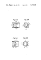
- FIG. 1A illustrates a schematic, cross-sectional view of the vapor growth apparatus according to one embodiment of the invention
- FIG. 1B illustrates a side view of FIG. 1A
- FIG. 2A illustrates a side elevational view of the reaction tube
- FIG. 2B is a sectional view taken along the line B--B of FIG. 2A;
- FIGS. 3 and 4 illustrate schematic side elevational views of the reaction tube for growing a thin film on the wafers
- FIG. 5A illustrates a partial cross-sectional view of the reaction tube, in which a vapor growth according to an embodiment of the invention is carried out
- FIG. 5B is a cross-sectional view taken along the line B--B in FIG. 5A;
- FIG. 6A is a similar figure to FIG. 5A;
- FIG. 6B is a cross-sectional view taken along the line B--B in FIG. 6A;
- FIG. 7 illustrates a schematic, cross-sectional view of the wafers with a thin film formed thereon, and
- FIG. 8 is a graph representing the relationship between the ratio H/W and P.
- the apparatus for carrying out an embodiment of the present invention is constructed as shown in FIGS. 1A and 1B.
- the inner wall of the reaction tube 1 defines a reaction chamber 2 which has a circular cross-section of a diameter L.
- the reaction gas are caused to flow, usually with the aid of a carrier gas, into the chamber 2 in the direction of the arrows 10 in FIG. 1.
- the heating means 3 for a resistance or induction heating surrounds the reaction tube 1.
- the wafers 5 are arranged in the reaction tube 1 at a constant distance H between every two adjacent exposed surfaces of the wafers. Each of the wafers 5 is made of two pieces of wafers 5a and 5b (as shown in FIG.
- the wafers 5 (FIG. 2A) are placed concentrically to the longitudinal axis of the reaction tube 1.
- the annular clearance is therefore formed between the peripheral edges of the pieces of wafers 5 and the inner wall of the reaction tube 1 (FIG. 1B).
- the radial width W of the clearance is expressed by the formula:
- a few pressure gauges (not shown) are communicated with the chamber 2 to measure the average pressure within the chamber 2.
- FIGS. 2A and 2B illustrate an example of the supporting means in the form of a base plate 4 having a recess 4a.
- Two pieces 5a, 5b of the wafers 5 are removably inserted into the recess 4a, in such a manner that the edge of each of the wafers 5 is placed on the base plate 4.
- the annular clearance 2a thus formed in the chamber of the reaction tube 1 surrounds the peripheral edge of each of the wafers except for the edge supported by the base plate 4.
- FIG. 2 illustrates an example of the supporting means 4 for positioning the wafers concentrically to the axis of the reaction tube 1.
- This means consists of two bases 4 secured to the inner wall of the reaction tube 1 and the two bases are separated from each other by an angle of approximately 60°.
- Each base 4 has a recess to removably support the wafer.
- the clearance between the peripheral edge of the wafers 5 and the inner wall of the reaction chamber has a constant thickness 2a around the wafer.
- FIGS. 3 and 4 illustrate the method of supporting the polygonal wafers 5 within the reaction chamber 1.
- wafers 5 of polygonal shape can be placed in a reaction tube having a polygonal shape similar to that of the wafers, in such a manner that the wafers are supported in an essentially concentric relationship to the axis of the reaction tube.
- the clearance between the peripheral edge of the polygonal wafers 5 and the inner wall of the reaction tube 1 has a constant thickness around the wafers.
- This constant thickness, denoted as W 1 to W 4 in FIG. 3 and W 1 to W 8 in FIG. 4 is determined according to the formulae (1) or (2), in order to grow a film having a uniform thickness on a plurality of pieces of the wafers.
- FIGS. 5A and 5B illustrate a preferable arrangement of the wafers 5 in the reaction tube 1, when the wafers 5 do not have a shape similar to the round reaction chamber 2, because the wafers 5 have a flat part 5a around the peripheral edge thereof.
- Each piece of the wafers 5 is removably secured to the disc plate 6, which can consist of one of carbon, silicon, alumina (Al 2 O 3 ), or SiO 2 .
- the axes of the wafers 5 and the plate 6 coincide with each other.
- the disc plate 6 is placed in the reaction tube 1 concentrically to the axis of the reaction tube 1, so that an annular clearance 2a, having an equal width W around the plate 6, is formed.
- FIGS. 6A and 6B illustrate another preferable arrangement of the non-similar wafers.
- the plate 6 has a part, denoted as 6a, which is of the same shape as the defficient part of the wafers 5a.
- the defficient part of the wafers 5 is supplemented by the part denoted as 6a of the plates 6, when the wafers 5 and the plates are viewed in the flowing direction of the reaction gas.
- the plates 6 can consist of the same material as the wafers and have the same size as the wafers.
- the combined body of these two wafers are surrounded by an annular clearance having the same width W around the entire inner peripheral wall of the reaction tube 1.
- a uniform film can, therefore, be grown on the exposed surface of each of the wafers.
- the film also grows on the exposed defficient part 5a of the wafer, however, such growth does not cause trouble from a technical point in view.
- the Si wafers were heated to a temperature of 850° C.
- the internal pressure of the reaction tube 1 was reduced by a vacuum pump (not shown in the FIGS).
- the reaction gas of monosilane SiH 4 with ammonia NH 3 were caused to flow from an inlet (not shown) to an outlet (not shown) of the reaction tube 1 in the direction depicted by the arrows 10 in FIG. 1.
- the average pressure inside the tube was adjusted to an almost constant value during the vapor growth while the reaction gas were flowing.
- the distance between two adjacent exposed surfaces of the wafers was maintained constant with regard to all the wafers involved. Since the distance was varied for four different cases, that is 5, 10, 15 and 20 mm, the ratios H/W, that is, 1, 2, 3 and 4, respectively, were accordingly obtained.
- the average pressure P was respectively varied at 4, 2, 1 and 0.5 Torr.
- the thickness distribution of one thin film was investigated in relation to the variances of the ratio H/W and to the variances of the pressure P. The results are illustrated in FIG. 7, wherein the view of the thickness of the thin film 8 has been enlarged with respect to that of the Si wafer 5, for a clear understanding of the thickness distribution of the thin film 8.
- the ratio H/W and the pressure P were varied below 6 and 6 Torr, respectively, and the respective pertinent ranges of H/W and P for obtaining a thin film with a desired distribution thereof were proved to be represented within the hatched area of FIG. 8.
- the largest value 1.2 of the constant "b” should be selected for the reaction gases (6) and (7) of this Example, and the smallest value 0.3 of the constant “b” should be selected for the reaction gas (4).
- the values of 0.5, 0.6 and 0.7 of the constant "b” should be selected for the reaction gas (1), (2) and (3), respectively.
- the preferable ratio H/W is 2 or a ⁇ P+0.3 in relation to the reaction gases (6) and (7), or in relation to the reaction gas (4), respectively.
- the pressure P is below 0.3 Torr, the growth rate of a thin film is too low.
Landscapes
- Chemical & Material Sciences (AREA)
- General Chemical & Material Sciences (AREA)
- Chemical Kinetics & Catalysis (AREA)
- Engineering & Computer Science (AREA)
- Materials Engineering (AREA)
- Metallurgy (AREA)
- Organic Chemistry (AREA)
- Mechanical Engineering (AREA)
- Crystallography & Structural Chemistry (AREA)
- Chemical Vapour Deposition (AREA)
Applications Claiming Priority (6)
| Application Number | Priority Date | Filing Date | Title |
|---|---|---|---|
| JP4492376A JPS52128890A (en) | 1976-04-22 | 1976-04-22 | Production of thin film by decompression gas phase growth process |
| JP51-44923 | 1976-04-22 | ||
| JP51-44922 | 1976-04-22 | ||
| JP4492276A JPS52129282A (en) | 1976-04-22 | 1976-04-22 | Growth method of thin film by reduced pressure vapor phase growth method |
| JP4850776A JPS52132675A (en) | 1976-04-30 | 1976-04-30 | Vapor-phase growth method of thin film |
| JP51-48507 | 1976-04-30 |
Publications (1)
| Publication Number | Publication Date |
|---|---|
| US4179326A true US4179326A (en) | 1979-12-18 |
Family
ID=27292066
Family Applications (1)
| Application Number | Title | Priority Date | Filing Date |
|---|---|---|---|
| US05/787,495 Expired - Lifetime US4179326A (en) | 1976-04-22 | 1977-04-14 | Process for the vapor growth of a thin film |
Country Status (6)
| Country | Link |
|---|---|
| US (1) | US4179326A (enExample) |
| DE (1) | DE2718026C3 (enExample) |
| FR (1) | FR2348983A1 (enExample) |
| GB (1) | GB1575578A (enExample) |
| IT (1) | IT1114781B (enExample) |
| SE (1) | SE432162B (enExample) |
Cited By (7)
| Publication number | Priority date | Publication date | Assignee | Title |
|---|---|---|---|---|
| US4389273A (en) * | 1978-12-21 | 1983-06-21 | U.S. Philips Corporation | Method of manufacturing a semiconductor device |
| US4411729A (en) * | 1979-09-29 | 1983-10-25 | Fujitsu Limited | Method for a vapor phase growth of a compound semiconductor |
| US4582020A (en) * | 1984-05-04 | 1986-04-15 | Anicon, Inc. | Chemical vapor deposition wafer boat |
| US4641604A (en) * | 1984-05-04 | 1987-02-10 | Anicon, Inc. | Chemical vapor deposition wafer boat |
| US4694778A (en) * | 1984-05-04 | 1987-09-22 | Anicon, Inc. | Chemical vapor deposition wafer boat |
| US4946543A (en) * | 1986-06-02 | 1990-08-07 | Kalisher Murray H | Method and apparatus for growing films on a substrate |
| CN108368608A (zh) * | 2015-07-09 | 2018-08-03 | 韩华Qcells有限公司 | 用于成对容纳衬底的设备 |
Families Citing this family (5)
| Publication number | Priority date | Publication date | Assignee | Title |
|---|---|---|---|---|
| DE3141567C2 (de) * | 1981-10-20 | 1986-02-06 | Siemens AG, 1000 Berlin und 8000 München | Verfahren zum Herstellen von aus Tantal, Wolfram oder Molybdän bestehenden Schichten bei niedrigen Temperaturen und Verwendung dieser Schichten |
| DE3530999A1 (de) * | 1985-08-30 | 1987-03-05 | Telefunken Electronic Gmbh | Verfahren zur herstellung von halbleiteranordnungen |
| GB2193976B (en) * | 1986-03-19 | 1990-05-30 | Gen Electric Plc | Process for depositing a polysilicon film on a substrate |
| GB2213836B (en) * | 1987-12-18 | 1992-08-26 | Gen Electric Co Plc | Vacuum deposition process |
| WO1998000215A1 (fr) * | 1996-07-02 | 1998-01-08 | Jury Viktorovich Klevkov | Procede permettant d'eliminer les impuretes de substances simples ou complexes |
Citations (6)
| Publication number | Priority date | Publication date | Assignee | Title |
|---|---|---|---|---|
| US3657004A (en) * | 1969-01-11 | 1972-04-18 | Siemens Ag | Method for producing highly pure gallium arsenide |
| DE2124392A1 (en) * | 1971-05-17 | 1972-11-30 | Siemens Ag | Doping germanium by diffusion - using source conditioned with moist oxygen, giving reproducibility and accuracy |
| DE2133876A1 (de) * | 1971-07-07 | 1973-01-18 | Siemens Ag | Anordnung zum eindiffundieren von dotierstoffen |
| DE2133843A1 (de) * | 1971-07-07 | 1973-01-18 | Siemens Ag | Anordnung zum eindiffundieren von dotierstoffen in halbleiterscheiben |
| US3922467A (en) * | 1973-04-27 | 1975-11-25 | Philips Corp | Vapour-phase deposition method |
| US4018183A (en) * | 1973-11-15 | 1977-04-19 | U.S. Philips Corporation | Apparatus for treating a plurality of semiconductor slices to a reacting gas current |
-
1977
- 1977-04-14 SE SE7704276A patent/SE432162B/xx not_active IP Right Cessation
- 1977-04-14 US US05/787,495 patent/US4179326A/en not_active Expired - Lifetime
- 1977-04-18 GB GB16011/77A patent/GB1575578A/en not_active Expired
- 1977-04-20 IT IT22668/77A patent/IT1114781B/it active
- 1977-04-22 DE DE2718026A patent/DE2718026C3/de not_active Expired
- 1977-04-22 FR FR7712288A patent/FR2348983A1/fr active Granted
Patent Citations (6)
| Publication number | Priority date | Publication date | Assignee | Title |
|---|---|---|---|---|
| US3657004A (en) * | 1969-01-11 | 1972-04-18 | Siemens Ag | Method for producing highly pure gallium arsenide |
| DE2124392A1 (en) * | 1971-05-17 | 1972-11-30 | Siemens Ag | Doping germanium by diffusion - using source conditioned with moist oxygen, giving reproducibility and accuracy |
| DE2133876A1 (de) * | 1971-07-07 | 1973-01-18 | Siemens Ag | Anordnung zum eindiffundieren von dotierstoffen |
| DE2133843A1 (de) * | 1971-07-07 | 1973-01-18 | Siemens Ag | Anordnung zum eindiffundieren von dotierstoffen in halbleiterscheiben |
| US3922467A (en) * | 1973-04-27 | 1975-11-25 | Philips Corp | Vapour-phase deposition method |
| US4018183A (en) * | 1973-11-15 | 1977-04-19 | U.S. Philips Corporation | Apparatus for treating a plurality of semiconductor slices to a reacting gas current |
Cited By (7)
| Publication number | Priority date | Publication date | Assignee | Title |
|---|---|---|---|---|
| US4389273A (en) * | 1978-12-21 | 1983-06-21 | U.S. Philips Corporation | Method of manufacturing a semiconductor device |
| US4411729A (en) * | 1979-09-29 | 1983-10-25 | Fujitsu Limited | Method for a vapor phase growth of a compound semiconductor |
| US4582020A (en) * | 1984-05-04 | 1986-04-15 | Anicon, Inc. | Chemical vapor deposition wafer boat |
| US4641604A (en) * | 1984-05-04 | 1987-02-10 | Anicon, Inc. | Chemical vapor deposition wafer boat |
| US4694778A (en) * | 1984-05-04 | 1987-09-22 | Anicon, Inc. | Chemical vapor deposition wafer boat |
| US4946543A (en) * | 1986-06-02 | 1990-08-07 | Kalisher Murray H | Method and apparatus for growing films on a substrate |
| CN108368608A (zh) * | 2015-07-09 | 2018-08-03 | 韩华Qcells有限公司 | 用于成对容纳衬底的设备 |
Also Published As
| Publication number | Publication date |
|---|---|
| DE2718026B2 (de) | 1979-10-11 |
| IT1114781B (it) | 1986-01-27 |
| FR2348983B1 (enExample) | 1979-03-09 |
| DE2718026A1 (de) | 1977-11-10 |
| DE2718026C3 (de) | 1984-06-07 |
| GB1575578A (en) | 1980-09-24 |
| SE432162B (sv) | 1984-03-19 |
| SE7704276L (sv) | 1977-10-23 |
| FR2348983A1 (fr) | 1977-11-18 |
Similar Documents
| Publication | Publication Date | Title |
|---|---|---|
| US4179326A (en) | Process for the vapor growth of a thin film | |
| JP2839720B2 (ja) | 熱処理装置 | |
| US5336327A (en) | CVD reactor with uniform layer depositing ability | |
| US5876797A (en) | Low temperature high pressure silicon deposition method | |
| US4263087A (en) | Process for producing epitaxial layers | |
| EP0784106A1 (en) | Epitaxial growth method | |
| US5685906A (en) | Method and apparatus for configuring an epitaxial reactor for reduced set-up time and improved layer quality | |
| US3682699A (en) | Method of vapor growth of a semiconductor crystal | |
| US5390626A (en) | Process for formation of silicon carbide film | |
| US4699825A (en) | Method of forming silicon nitride film and product | |
| US20240401201A1 (en) | Window for chemical vapor deposition systems and related methods | |
| JP3788836B2 (ja) | 気相成長用サセプタ及びその製造方法 | |
| GB2212173A (en) | Heated reactor for vapor-phase growth of films | |
| US3816166A (en) | Vapor depositing method | |
| JPS62214614A (ja) | 減圧cvd装置 | |
| JP2762576B2 (ja) | 気相成長装置 | |
| EP0731492A2 (en) | Method of growing a single crystal thin film with a uniform thickness, in the vapor phase | |
| JP3076268B2 (ja) | 減圧気相成長装置 | |
| JPS5941773B2 (ja) | 気相成長方法及び装置 | |
| EP4525023A1 (en) | Epitaxial wafer | |
| JPH01123413A (ja) | 気相成長装置 | |
| JPH024973A (ja) | 膜形成方法 | |
| JPS5493357A (en) | Growing method of polycrystal silicon | |
| JPS6191920A (ja) | エピタキシヤル成長方法 | |
| JPH0319324A (ja) | 気相成長装置 |