US20030190794A1 - Semiconductor substrate and process for producing the same using a composite member having porous layers and varying thickness and porosity - Google Patents
Semiconductor substrate and process for producing the same using a composite member having porous layers and varying thickness and porosity Download PDFInfo
- Publication number
- US20030190794A1 US20030190794A1 US09/047,338 US4733898A US2003190794A1 US 20030190794 A1 US20030190794 A1 US 20030190794A1 US 4733898 A US4733898 A US 4733898A US 2003190794 A1 US2003190794 A1 US 2003190794A1
- Authority
- US
- United States
- Prior art keywords
- porous
- layer
- substrate
- thickness
- porous layer
- Prior art date
- Legal status (The legal status is an assumption and is not a legal conclusion. Google has not performed a legal analysis and makes no representation as to the accuracy of the status listed.)
- Abandoned
Links
Images



Classifications
-
- H—ELECTRICITY
- H10—SEMICONDUCTOR DEVICES; ELECTRIC SOLID-STATE DEVICES NOT OTHERWISE PROVIDED FOR
- H10P—GENERIC PROCESSES OR APPARATUS FOR THE MANUFACTURE OR TREATMENT OF DEVICES COVERED BY CLASS H10
- H10P90/00—Preparation of wafers not covered by a single main group of this subclass, e.g. wafer reinforcement
- H10P90/19—Preparing inhomogeneous wafers
- H10P90/1904—Preparing vertically inhomogeneous wafers
- H10P90/1906—Preparing SOI wafers
- H10P90/1914—Preparing SOI wafers using bonding
Definitions
- the present invention relates to a process for producing a semiconductor substrate, and more particularly a process for producing a semiconductor substrate provided with a plurality of porous layers.
- SOI semiconductor-on-insulator
- the devices formed on a compound semiconductor have excellent features, such as a high speed, light emission or the like, which are not achievable with those on a silicon substrate.
- the devices are mostly formed in a layer epitaxially grown on a compound semiconductor substrate such as GaAs or the like.
- the compound semiconductor substrates are associated with drawbacks such as expensiveness, a low mechanical strength and difficulty of preparation of a large-area wafer.
- the CVD method necessitates sacrifice oxidation for obtaining a flattened thin film, while the solid-phase growth method is insufficient in the crystallinity.
- the beam annealing method has problems in the processing time required by the focused beam scanning and in the controllability of beam overlapping degree and beam focusing.
- the zone melting recrystallization method is most advanced to a level that relatively large-scale integrated circuits have been experimentally manufactured, but the substrate still contains large number of crystal defects such as sub grain boundaries and has not reached a level enough for the preparation of minority carrier devices.
- So-called SIMOX (separation by ion implanted oxygen) method utilizes formation of an SiO 2 layer by oxygen ion implantation into an Si single-crystal substrate and is currently most advanced because of the good matching with the Si process.
- the formation of an SiO 2 layer requires oxygen ion implantation of 10 18 ions/cm 2 or larger, thus necessitating a very long implantation time, leading to a limited productivity and a high wafer cost. Also there still remains a large number of crystal defects, and this method has not industrially reached a product quality enough for producing the minority carrier devices;
- (c) There is also known a method of forming the SOI structure by dielectric isolation by oxidation of porous Si.
- This method consists of forming an N-type Si layer in an island shape on a surface of a P-type Si single-crystal substrate either by proton ion implantation (Imai et al., J. Crystal Growth, Vol. 63, 547 (1983)) or by epitaxial growth and patterning, then effecting anodization in an HF solution from the surface so as to surround the Si island to thereby make only the P-type Si substrate porous, and effecting dielectric isolation of the N-type Si island by accelerated oxidation.
- the isolated Si area is defined prior to the device process so that the freedom of device designing may be limited; and
- the method (a) is difficult to provide a uniform thin film.
- the fluctuation in thickness becomes as high as several tens of percent and the difficulty becomes severer with the increase in the wafer diameter.
- the method (b) is considered effective for obtaining a uniform thin film, but is associated with the following limitations:
- selectivity being about 10 2 , is not sufficient
- crystallinity of the semiconductor layer on the insulating film (SOI layer) is insufficient because epitaxial or heteroepitaxial growth is utilized on the highly B-doped Si layer formed by ion implantation (C. Harendt et al., J. Elect. Mater., Vol. 20, 267 (1991), H. Baumgart et al., Extended Abstract of ECS 1st International Symposium of Wafer Bonding, pp. 733 (1991), C. E. Hunt, Extended Abstract of ECS 1st International Symposium of Wafer Bonding, pp. 696 (1991)).
- the semiconductor substrate employing the bonding always necessitates two wafers, one of which is mostly eliminated by polishing or etching, thus resulting in significant waste of the limited resources of the earth.
- a thin film Si layer deposited thereon usually becomes amorphous or polycrystal at best, reflecting the disorder of the substrate, so that a high-performance device cannot be prepared. This is based on a fact that the substrate is amorphous, and a mere deposition of an Si layer thereon will not provide a fine quality single-crystal layer.
- such a light-transmissive substrate is important in constructing a contact sensor which is a light receiving element, or a projection-type liquid crystal image display device, and, for forming the pixels (image elements) of such a sensor or display device with a higher density, a higher resolution and a higher precision, there are required driving elements of higher performance. Consequently, the devices provided on the light-transmissive substrate have to be prepared with a single-crystal layer of excellent crystallinity.
- a compound semiconductor substrate is essential for producing a compound semiconductor device.
- the compound semiconductor substrate is expensive, and the preparation of the large-area substrate is extremely difficult.
- the method of forming a non-porous single-crystal semiconductor layer on a porous layer and transferring the semiconductor layer onto a support substrate via an insulation layer is superior in consideration of the excellent thickness uniformity of the SOI layer, easy control of the crystal defect density of the SOI layer at a low level, excellent surface flatness of the SOI layer, absence of necessity for an expensive manufacturing apparatus of special specifications, and possibility of production, in the same apparatus, of SOI films of a wide thickness range from several hundred Angstroms to about 10 micrometers.
- the separation of the bonded wafers at the porous layer is generally possible using the above-mentioned method, there still remain certain problems to be solved.
- the separation of the bonded wafers at the porous layer may result in a partial destruction of the first or second substrate, or in introduction of defects such as cracks or dislocations into the non-porous single-crystal semiconductor layer formed on the porous layer.
- the separation at the porous layer can not be attained though the reason is unclarified and the frequency of such phenomenon is low.
- the separation of the bonded substrates becomes easier, but the porous layer may be broken in advance in any one of the steps from the anodization step for forming the porous layer to the completion of the bonding step.
- Such premature destruction may render the bonding step impossible or may cause contamination of the production steps by the particles generated from the broken porous layer or from the non-porous single-crystal layer formed thereon.
- the porous layer is peeled off even in a part in the course of the anodization in the anodizing apparatus, it becomes no longer possible to uniformly form a non-porous single-crystal layer on a substrate of such a substrate.
- Such peeling off of the porous layer prior to the bonding step may be caused not only in the anodizing step but also in any step before or after the bonding step, such as a subsequent oxidation step in a heating oven, a subsequent non-porous semiconductor layer forming step in a CVD apparatus or the like, an annealing step in a heating oven after the bonding step for improving the bonding strength, or a cleaning step required repeatedly between the respective steps.
- An object of the present invention is to provide a semiconductor substrate in which the destruction of the porous region is difficult to occur prior to the separation of the bonded substrates, and a process for producing the same.
- Another object of the present invention is to provide a semiconductor substrate in which the separation takes place reproducible at a predetermined position of the porous region, and a process for producing the same.
- Still another object of the present invention is to provide a semiconductor substrate capable of inexpensively providing an SOI substrate of satisfactory quality, and a process for producing the same.
- the porous region is formed such that the porous region comprises a first porous layer adjacent to the non-porous semiconductor layer and a second porous layer having a higher porosity and a smaller thickness than those of the first porous layer, and such that the thickness of the second porous layer is not more than 80% of the thickness of the first porous layer and the porosity of the second porous layer is from 30% to 60%.
- a composite member for a semiconductor substrate comprising a first substrate, a porous region provided on the first substrate, a non-porous semiconductor layer provided on the porous region, and a second substrate provided on the non-porous semiconductor layer;
- the porous region comprises a first porous layer adjacent to the non-porous semiconductor layer and a second porous layer having a higher porosity and a smaller thickness than those of the first porous layer, and wherein the thickness of the second porous layer is not more than 80% of the thickness of the first porous layer and the porosity of the second porous layer is from 30% to 60%.
- porous layer refers to the proportion of the volume as occupied by the pores with respect to the material constituting the porous layer, within the volume of the porous layer.
- the porosity of the second porous layer is maintained within a range from 30% to 60%, preferably from 40% to 60%.
- the separation is still possible at a porosity lower than such a range.
- there is a case where during the separation there may result a partial destruction, a crack or a slip dislocation in the first or the second substrate or in the non-porous layer formed on the porous layer of the first substrate.
- the porosity is maintained in the range of 30% to 60%.
- t1 thickness of the first porous layer adjacent to the non-porous semiconductor layer
- t2 thickness of the second porous layer
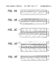
- FIGS. 1A, 1B, 1 C and 1 D are schematic cross-sectional views showing a basic process for producing a semiconductor substrate of the present invention
- FIGS. 2A, 2B, 2 C, 2 D and 2 E are schematic cross-sectional views showing an embodiment of the process for producing a semiconductor substrate of the present invention
- FIGS. 3A, 3B, 3 C, 3 D and 3 E are schematic cross-sectional views showing another embodiment of the process for producing a semiconductor substrate of the present invention.
- FIGS. 4A, 4B, 4 C, 4 D and 4 E are schematic cross-sectional views showing still another embodiment of the process for producing a semiconductor substrate of the present invention.
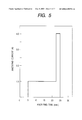
- FIG. 5 is a chart showing the relationship between the anodizing time and the anodizing current of the anodization employed in the present invention
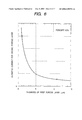
- FIG. 6 is a chart showing the relationship between the thickness of the first porous layer and the anodizing current for forming the second porous layer.
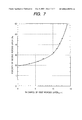
- FIG. 7 is a chart showing the relationship between the thickness of the first porous layer and the porosity of the second porous layer.
- FIG. 1A there is prepared a first substrate 10 provided with a porous region 1 and a non-porous semiconductor layer 13 provided on the porous region 1 .
- the porous layer 1 is so formed as to have a structure including at least a first porous layer 11 adjacent to the non-porous semiconductor layer 13 and a second porous layer 12 .
- the porosity P2 of the second porous layer 12 is so selected as to be higher than the porosity P1 of the first porous layer 11 , and the porosity P2 is selected within a range from 30% to 60%.
- the thickness t2 of the second porous layer 12 is so selected as not to exceed 80% of the thickness t1 of the first porous layer 11 .
- the first substrate 10 and a second substrate 14 are bonded to each other via an insulating layer 15 to obtain a composite member 2 for forming the semiconductor substrate.
- the insulating layer 15 is preferably formed, prior to the bonding, on at least either of the surfaces of the first substrate 10 and the second substrate 14 .
- the first and the second substrates are separated, whereupon the separation takes place at the interface of the first porous layer 11 and the second porous layer 12 , or at a portion of the second porous layer close to the above-mentioned interface, or at a portion including the entire second porous layer.
- a remnant layer 11 b of a uniform thickness resulting from the first porous layer 11 remains on the second substrate.
- the separated first substrate 10 can be used again as the first or second substrate.
- the starting material for the first substrate prior to the formation of the porous region 1 is preferably selected from semiconductor materials such as Si, Ge, GaAs, InP, SiC or SiGe.
- the porous region may either be formed by making the surface of the starting material porous or be additionally formed on the surface of the starting material.
- the porosity P (%) indicates the proportion of volume of the pores, within the volume of the porous layer, with respect to the material constituting the porous layer.
- the porosity is represented as follows, by using the density m of the porous member and the density M of a non-porous member of the same material as that of the porous member:
- the porosity P (%) of the porous layer of the first substrate of which the surface layer only down to a depth d from the surface is porous is determined by:
- A is the weight of the first substrate prior to the formation of the porous layer
- a is the weight of the first substrate after the formation of the porous layer
- B is the weight of the first substrate after complete removal of the porous layer.
- the porosity of the first porous layer is desirably less than 30%, preferably not more than 20%.
- the porosity of the second porous layer is desirably selected to be not less than 30%, more preferably not less than 40%, and to be not more than 60%. Such selection is to reduce the portion constituting the walls of the pores in the porous layer, thereby rendering the porous structure more fragile and facilitating the destruction thereof at that portion.
- the second porous layer can be made thin, for the purpose of separation of the bonded substrates.
- a thickness of at least 50 nm, preferably at least 100 nm, is effective for the separation of the substrates.
- an excessively small thickness leads to a difficulty in the precise control of the thickness of the second porous layer.
- an excessively large thickness of the second porous layer may result in peeling off of the first porous layer prior to the bonding, even if the porosity of the second porous layer is not so high. In order to prevent such peeling, it is effective to form the second porous layer thinner than the first porous layer. As an internal stress is generated in the portion of a lower porosity, the portion of a higher porosity, if formed thicker than the portion of the lower porosity, becomes excessively weak and may be broken prior to the bonding whereby the portion of the lower porosity may be peeled off. Even if the first porous layer is considerably thick, it is not desirable to form the second porous layer thicker than 3 ⁇ m.
- the thickness of the second porous layer is so selected as not to exceed 3 ⁇ m. More specifically, in consideration of the ease of separation, the thickness of the second porous layer is selected within a range from 1 nm to 1 ⁇ m for a substrate not exceeding 6 inches in diameter, and within a range from 1 to 3 ⁇ m for a substrate of 8 inches or larger in diameter.
- a layer of a porosity between those of the first and the second porous layers, between the first and the second porous layers or at a side of the second porous layer opposite to the first porous layer.
- the stress at the separation is concentrated on a layer of the highest porosity, which thus functions as the second porous layer.
- porous Si though being dependent on the level of porosity, is considered sufficiently lower than that of bulk Si.
- the porous layer can be broken with a weaker force with the increase in the level of porosity. If the porous layer is composed of a plurality of layers of different porosities, the stress will be concentrated in a layer of the highest porosity, where the destruction begins.
- An Si substrate can be made porous by anodization utilizing an HF solution.
- the density of the porous Si layer can be varied within a range of 1.1-0.6 g/cm 3 by a change of the concentration of the HF solution within a range of 50-20%.
- the porous layer is not easily formed in an N-type Si layer but easily formed in a P-type Si substrate because of the reason explained below. According to the observation with a transmission electron microscope, the porous Si layer contains pores of 100-600 ⁇ in average diameter.
- porous Si was found by Uhlir et al. in 1956 in the course of investigation of electropolishing of semiconductor (A. Uhlir, Bell Syst. Tech. J., Vol. 35, 333 (1956)).
- e + and e ⁇ respectively represent a positive hole and an electron.
- n and ⁇ indicate the number of positive holes required for dissolving a Si atom, and it was reported the porous Si was formed when a condition n>2 or ⁇ >4 is satisfied.
- the P-type Si containing positive holes can be made porous but the N-type Si is not made so.
- This selectivity in porous structure formation was proved by Nagano et al. and Imai (Nagano, Nakajima, Yasuno, Ohnaka and Kajiwara, Technical Research Report of Electronic Communications Society, Vol. 79, SSD79-9549 (1979), K. Imai, Solid-State Electronics, Vol. 24, 159 (1981)). It is however also reported that porous structure formation is possible in the n-type Si if the impurity concentration is high (R. P. Holmstrom and J. Y. Chi, Appl. Phys. Lett., Vol. 42, 386 (1983)), so that it is important to select a substrate allowing porous structure formation, regardless of P or N type.
- the porous Si layer contains pores of about 100-600 ⁇ in average diameter.
- the single-crystallinity is maintained even when the density is reduced less than half of that of single-crystal Si, so that it is possible to epitaxially grow a single-crystal Si layer on the porous layer.
- a low-temperature growth method such as molecular beam epitaxial growth, plasma CVD, low pressure CVD, photo CVD, bias sputtering or liquid phase growth is considered adequate for the epitaxial growth of the Si layer.
- the porous layer has a large amount of voids formed therein, its density is reduced to less than half. As a result, the surface area increases drastically in comparison with the volume, so that the chemical etching rate thereof is significantly increased in comparison with that of the ordinary single-crystal layer.
- the non-porous semiconductor layer to be employed in the present invention consists of a single layer or plural layers of a semiconductor such as Si, Ge, GaAs, InP, SiC, SiGe, GaN or GaP.
- the respective layers may be different from each other in conductivity type or electric conductivity, or may be those which form a hetero junction therebetween.
- the non-porous semiconductor layer may be formed by depositing a non-porous semiconductor layer on the porous region, or by forming a porous layer, for example by ion implantation, under the surface layer of a non-porous starting material, and employing the surface layer, which remains without being made porous state, as the non-porous semiconductor layer.
- the second substrate employed in the present invention may be selected from semiconductors such as Si, Ge, SiC, SiGe, GaAs or InP, or from insulating materials such as quartz, fused quartz, silica glass, glass, sapphire or the like.
- the method for separating the bonded substrates there may be employed any of the separation methods disclosed in Japanese Patent Application Laid-Open No. 7-302889, for example irradiation with wave energy such as ultrasonic wave, insertion of a separating member from a side surface of the porous layer parallel to the bonded surface of the bonded substrates, utilization of expanding energy of a material impregnated in the porous layer, selective etching of the porous layer from a side surface of a disk-like substrate, or exposing the porous layer and oxidizing the porous layer from a side surface thereof and utilizing the volume expansion at the oxidation.
- wave energy such as ultrasonic wave
- FIGS. 2A to 2 E show a process for producing a semiconductor substrate, based on the basic process shown in FIGS. 1A to 1 D and constituting an embodiment of the present invention.
- first porous layer 11 As shown in FIG. 2A, on the surface of a first substrate 10 , there are formed a first porous layer 11 and a second porous layer 12 .
- the porosity of the second porous layer 12 is selected to be not less than 30%, while that of the first porous layer 11 is selected to be less than 30%.
- the thickness of the second porous layer 12 is so selected as to be not more than 0.8 times of that of the first porous layer 11 .
- the first and the second porous layers as defined above can be advantageously formed by anodization.
- the current is increased to make porous the non-porous portion of the first substrate under the first porous layer, thereby forming the second porous layer 12 .
- the anodizing liquid may be replaced to form the second porous layer 12 by the anodization under the same current.
- a non-porous semiconductor layer 13 is formed on the porous layer 11 , and the surface of the non-porous semiconductor layer 13 is made insulating, if necessary.
- a support substrate 17 having a second substrate 14 and bearing an insulating layer 15 thereon and a substrate 16 having the first substrate 10 bearing the above-described layers 11 , 12 , 13 are brought into close contact with each other at room temperature, and the substrates are bonded to each other by anodic bonding, pressure application, heat treatment or a combination thereof.
- the second substrate 14 and the non-porous semiconductor layer 13 are firmly bonded via the insulating layer 15 .
- the insulating layer 15 is formed on at least either of the non-porous semiconductor layer 13 and the second substrate 14 . Otherwise the bonding may be made with three members, including an insulating thin plate.
- the bonded members are separated into a substrate 18 and a substrate 19 at the porous Si layer 12 as shown in FIG. 2D.
- the substrate 19 is composed of the first porous layer 11 , the non-porous semiconductor layer 13 , the insulating layer 15 and the substrate 14 .
- porous layer 11 is selectively removed.
- the porous layer 11 alone is etched off by electroless wet chemical etching with at least one of an ordinary Si etching solution, hydrofluoric acid which is selective etching liquid for porous Si, a mixture of hydrofluoric acid and at least either of alcohol and aqueous hydrogen peroxide solution, buffered hydrofluoric acid and a mixture of buffered hydrofluoric acid and at least either of alcohol and aqueous hydrogen peroxide solution, thereby leaving and forming the non-porous semiconductor layer 13 transferred onto the insulating layer 15 (FIG. 2E).
- FIG. 2E shows the semiconductor substrate obtained by the present invention, wherein, on the substrate 14 with an insulating surface, the non-porous semiconductor layer 13 is formed as a flat and uniform thin layer, with few crystal defects.
- FIGS. 3A to 3 E show a variation of the semiconductor substrate producing process shown in FIGS. 2A to 2 E, employing a light-transmissive insulating substrate as the second substrate.
- the steps shown in FIGS. 3A and 3B are the same as those shown in FIGS. 2A and 2B.
- a light-transmissive insulating substrate 24 represented by quartz or glass and a first substrate 26 are brought into close contact with each other at room temperature, and the substrates are mutually bonded to each other by anodic bonding, pressure application, heat treatment or a combination thereof.
- the light-transmissive insulating substrate 24 and the non-porous semiconductor layer 13 are firmly bonded to each other via the insulating layer 15 .
- the insulating layer 15 is formed on at least either of the non-porous semiconductor layer 13 and the light-transmissive insulating substrate 24 . Otherwise the bonding may be made with three members, including an insulating thin plate.
- the bonded members are separated into a substrate 28 and a substrate 29 .
- the light-transmissive insulating substrate 24 there is formed a multi-layered structure consisting of the first porous layer 11 , the non-porous semiconductor layer 13 and the insulating layer 15 .
- porous layer 11 is selectively removed.
- the porous layer 11 alone is etched off by electroless wet chemical etching with at least one of ordinary Si etching liquid, hydrofluoric acid which is selective etching liquid for porous Si, a mixture of hydrofluoric acid and at least either of alcohol and aqueous hydrogen peroxide solution, buffered hydrofluoric acid, and a mixture of buffered hydrofluoric acid and at least either of alcohol and aqueous hydrogen peroxide solution, thereby leaving and forming the non-porous semiconductor layer 13 on the light-transmissive insulating substrate 24 . Because of the very large surface area of the porous member as described above, it is possible to selectively etch the porous member only and to leave the non-porous member even with the ordinary etching liquid.
- FIG. 3E shows the semiconductor substrate obtained by the present invention, wherein, on the surface of the light-transmissive insulating substrate 24 , the non-porous semiconductor layer 13 is formed as a flat and uniform thin layer with a large area, over the entire region of the substrate.
- the first substrate 10 is subjected to removal of the remaining porous layer 12 and, if the surface flatness is unacceptably coarse, additionally to the surface flattening treatment, and is used again as the first substrate 10 .
- FIGS. 4A to 4 E show a process of forming a porous layer and a non-porous semiconductor layer on each surface of a substrate and bonding three substrates.
- a first substrate 30 is prepared, and, in the surface portions on the both surfaces, there are formed two-layer-structure porous regions consisting of two layers 31 , 32 and 33 , 34 of different porosities, respectively and there are further formed non-porous semiconductor layers 35 , 36 on the first porous layers 31 , 32 (see FIG. 4B).
- the anodization is so conducted that the first porous layers 31 , 33 have a porosity less than 30% while the second porous layers 32 , 34 have a porosity not less than 30%.
- two second substrates 39 , 40 and the first substrate 30 having the non-porous semiconductor layers 35 , 36 are brought into close contact with each other at room temperature respectively via insulating layers 36 , 37 , and the substrates are mutually bonded to each other by anodic bonding, pressure application, heat treatment or a combination thereof.
- the substrates 39 , 40 and the non-porous semiconductor layers 35 , 36 are firmly bonded via the insulating layers 37 , 38 .
- the insulating layers 37 , 38 are formed on at least either of the non-porous semiconductor layers 35 , 36 and the substrates 39 , 40 . Otherwise separate insulating thin plates are prepared as the layers 35 , 36 and inserted between the substrates to achieve the bonding wit five members.
- each of the substrates 39 , 40 has a stacked structure consisting of the porous layer, the non-porous semiconductor layer and the insulating layer.
- porous layers 31 , 33 are selectively removed by polishing or etching, whereby thin non-porous semiconductor layers 35 , 36 are left on the substrates 39 , 40 .
- FIG. 4E shows the semiconductor substrates obtained by the present invention, wherein, on the substrates 39 , 40 , the non-porous semiconductor layers 35 , 36 are formed at the same time as flat and uniform thin layers.
- the intermediate insulating layers 37 , 38 may be omitted, and the substrates 39 , 40 need not be of the same material.
- the first substrate 30 is subjected to removal of the remaining porous layer or to the surface flattening treatment, and is used again.
- the porosity of the porous layer can be varied in the direction of thickness for example by a change in the anodizing current in the course of anodization for forming the porous layer, or by a change in the concentration of the anodizing liquid.
- the porosity and the pore size of the porous layer can be varied by a change in the concentration of an anodizing liquid using HF or in the anodizing current, as disclosed in SOLID-STATE SCIENCE AND TECHNOLOGY, Journal of Electrochemical Society, Vol. 134, No. 8, p. 1994.
- the composition of the anodizing liquid may be changed for example by the subsequent addition of hydrofluoric acid or water.
- Plural layers different in porosity can be formed, for example by at first forming a porous layer of a low porosity with an anodizing liquid of a high HF concentration, then forming a porous layer of a high porosity by replacing the anodizing liquid with another one of a lower HF concentration.
- a mere increase in the anodizing current does not provide a corresponding increase in the porosity but may result in an increased anodizing rate with a limited increase in the porosity.
- the simplest method in practice is of changing the anodizing current without change in the composition of the anodizing liquid.
- Various compositions can be employed for the anodizing liquid.
- satisfactory results can be obtained with hydrofluoric acid containing HF in about 30% or such hydrofluoric acid further added with alcohol.
- the anodization is conducted in such an anodizing liquid, and porous Si with porosity of 20 to 30% can be formed with a DC anodizing current density of 0.5-1.0 A/cm 2 using an Si substrate as the anode.
- the thickness of the porous Si can be arbitrarily selected depending on the anodizing time, and such a porous Si layer of a relatively low porosity is adequate for epitaxially growing thereon single-crystal Si.
- the current is increased to form a porous layer of a higher porosity.
- FIG. 5 shows an example of the mode of current variation.
- the first porous layer has a porosity of about 20% and a thickness of about 10 ⁇ m
- the second porous layer with a porosity of about 30 to 60% can be formed under the first porous layer, by setting the anodizing current to 2 to 3 times of that for forming the first porous layer.
- the porosity of the second porous layer is dependent not only on the magnitude of the anodizing current but also on the thickness and porosity of the first porous layer. Even when the anodizing current for the second porous layer is set to be the same as that for the first porous layer, if the first porous layer has a larger thickness or lower porosity, the porosity of the second porous layer tends to become higher. Consequently, if the first porous layer is made thinner, the anodizing current for the second porous layer has to be made higher in order to maintain a high porosity level therein. This relationship is shown in FIG. 6.
- the porosity of the second porous layer is affected by the change in the thickness of the first porous layer. This relationship is shown in FIG. 7. It will be evident that the formation of the second porous layer after the formation of the first porous layer cannot be independent therefrom but the porosity of the second porous layer is affected by the characteristics of the first porous layer. The detailed mechanism of such phenomenon is not yet fully clarified.
- the formation of the porous Si is considered to require F ⁇ ions in the anodizing liquid, and, as F ⁇ ions are consumed in a pore forming portion at the front end of a pore, new F ⁇ ions have to be transported through the pore and supplied to such front end portion.
- the effective mobility of F ⁇ ions by transportation through the pore by an electric field or by diffusion is considered to depend on the pore size of the first porous layer or the length of pore, namely the thickness of the first porous layer.
- the first porous layer itself formed by anodization limits the ion transportation required in the formation of a subsequent porous layer.
- the formed first porous layer functions as a layer for limiting the effective mobility of the F ⁇ ion transportation required for the subsequent porous layer formation.
- the anodization proceeds to a considerable thickness without a significant change in the porosity. This is presumably because, under a constant current, the pores are formed with a size determined by the balance of consumption and supply of F ⁇ ions but, if the current is increased in the course of anodization, the balance of consumption and supply of F ⁇ ions is changed by the presence of an already formed porous layer, thereby resulting in a significant change in the pore size.
- the F ⁇ ion concentration at the front end of the pore may become lower to expand an ion depletion layer in the anodizing liquid in the pore, whereby the portion may spread in which the potential barrier at the interface between the anodizing liquid and the single crystal Si surface in the pore become lower, thereby inducing etching of Si in such a portion to increase the pore size.
- a mere increase in the anodizing current does not cause a significant increase in the porosity but induces an increase in the anodizing rate unless a mobility limiting layer is present on the Si surface.
- the present invention is featured also by making the most of the above-described mechanism of anodization, utilizing the initially formed first porous layer for attaining increase of the porosity of the second porous layer.
- the first porous layer is required to have a certain thickness, and a high-porosity second porous layer can be easily formed when the first porous layer is 5 ⁇ m or more in thickness.
- the control of the thickness thereof is important for the porosity control of the second porous layer.
- the in-plane-uniformity of the first porous layer has to be secured sufficiently, since otherwise the porosity of the second porous layer fluctuates in plane.
- the presence of in-plane-fluctuation of the porosity of the second porous layer results in local fluctuation of the strength of the second porous layer, eventually leading to a partial peeling off of the second porous layer in the course of the SOI wafer production process or a locally incomplete separation at the separation step, whereby the production yield of the SOI wafer is lowered.
- the fluctuation within the substrate plane in thickness of the first porous layer has to be 35% or less, preferably 25% or less.
- the thickness of the first porous layer is made significantly less than 5 ⁇ m, in particular not more than 3 ⁇ m, the increase in porosity becomes progressively difficult since the effect of the mobility limiting layer described above is reduced.
- the anodizing current for the second porous layer has to be increased infinitely.
- Such increase in the current is naturally not impossible, but involves certain sacrifices such as an increase in the required power supply capacity, a resulting lowering in the precision of current control and a decrease in the precision of current measurement.
- an increased current leads to a higher anodizing rate, with possible lowering in the precision in the thickness control of the second porous layer. In such a case, all the requirements need not be satisfied by the current control only.
- a lowered HF concentration in the anodizing liquid can facilitate the decrease of F ⁇ ion concentration at the front end of the pore.
- the above-mentioned mobility limiting layer is still absent, so that sufficiently reducing the anodizing current can sufficiently supply the consumed F ⁇ ions, even if the HF concentration is lowered by a certain extent, and the porosity therefore scarcely increases.
- the porosity can be suppressed at about 20% if the anodizing current is limited to about 1 mA/cm 2 or less.
- the above-mentioned mobility limiting layer is already present, so that the deficiency in F ⁇ ions can be created at the front end of the pore even with a limited increase of the anodizing current, whereby the porosity can be increased.
- the second porous layer with a porosity as high as 30-60% by a mere increase of the anodizing current to about 5 mA/cm 2 .
- the substrate may be cleaned to remove the anodizing liquid depositing thereon or may be dried during such interruption.
- This Si wafer was then oxidized for 1 hour at 400° C. in oxygen atmosphere, whereby the internal wall surfaces of the pores in the porous Si were covered with a thermal oxide film. Then a single-crystal Si layer was epitaxially grown with a thickness of 0.3 ⁇ m by CVD on the porous Si, thereby forming a non-porous single-crystal Si layer on the porous Si, under the following growing conditions: Source gas: SiH 4 Carrier gas: H 2 Temperature: 850° C. Pressure: 1.3 Pa Growing rate: 3.3 nm/sec
- the porous layer was made to be exposed at the edge surface of the wafers and the porous Si at the edge portion was removed by a certain amount by etching, and a sharp-edged plate such as a razor blade was inserted therein, whereby the wafers were separated by the destruction of the porous Si layer and the porous Si was exposed.
- porous Si layer was selectively etched with an HF/H 2 O 2 /H 2 O etching solution, whereby the porous Si layer was completely removed.
- the first Si wafer was subjected to removal of the remaining porous Si and was used again as the first substrate.
- This wafer was then oxidized for 1 hour at 400° C. in oxygen atmosphere, whereby the internal wall surfaces of the pores in the porous Si were covered with a thermal oxide film. Then a single-crystal Si layer was epitaxially grown with a thickness of 0.3 ⁇ m by CVD on the porous Si, under the following growing conditions: Source gas: SiH 4 Carrier gas: H 2 Temperature: 850° C. Pressure: 1.3 Pa Growing rate: 3.3 nm/sec
- the porous layer was made to be exposed at the edge surface of the wafers and the porous Si at the edge portion was removed by a certain amount by etching, and a sharp-edged plate such as a razor blade was inserted therein, whereby the wafers were separated by the destruction of the porous Si layer and the porous Si was exposed.
- porous Si layer was selectively etched with an HF/H 2 O 2 /H 2 O etching solution, whereby the porous Si layer was completely removed.
- This wafer was then oxidized for 1 hour at 400° C. in oxygen atmosphere, whereby the internal wall surfaces of the pores in the porous Si were covered with a thermal oxide film. Then a single-crystal Si was epitaxially grown with a thickness of 0.3 ⁇ m by CVD on the porous Si under the following growing conditions: Source gas: SiH 4 Carrier gas: H 2 Temperature: 850° C. Pressure: 1.3 Pa Growing rate: 3.3 nm/sec
- the porous layer was made to be exposed at the edge surface of the wafers and the porous Si at the edge surface was removed by a certain amount by etching, and a sharp-edged plate such as a razor blade was inserted therein, whereby the wafers were mutually separated by the destruction of the porous Si layer and the porous Si was exposed.
- porous Si layer was selectively etched with an HF/H 2 O 2 /H 2 O etching solution, whereby the porous Si layer was completely removed.
- This wafer was then oxidized for 1 hour at 400° C. in oxygen atmosphere, whereby the internal wall surfaces of the pores in the porous Si were covered with a thermal oxide film. Then a single-crystal Si was epitaxially grown with a thickness of 0.3 ⁇ m by CVD on the porous Si, under the following growing conditions: Source gas: SiH 4 Carrier gas: H 2 Temperature: 850° C. Pressure: 1.3 Pa Growing rate: 3.3 nm/sec
- Plates were bonded, with an adhesive, on both the external surfaces of the bonded wafers, and a sufficient pressure was applied uniformly on such plates in a direction perpendicular to the external surfaces of the bonded wafers, whereby the wafers were mutually separated by the destruction of the porous Si layer and the remaining portion of the porous Si was exposed.
- porous Si layer was selectively etched with an HF/H 2 O 2 /H 2 O etching solution, whereby the porous Si layer was completely removed.
- This wafer was then oxidized for 1 hour at 400° C. in oxygen atmosphere, whereby the internal wall surfaces of the pores in the porous Si were covered with a thermal oxide film. Then a single-crystal Si layer was epitaxially grown with a thickness of 0.3 ⁇ m by CVD on the porous Si, under the following growing conditions: Source gas: SiH 4 Carrier gas: H 2 Temperature: 850° C. Pressure: 1.3 Pa Growing rate: 3.3 nm/sec
- the porous layer was made to be exposed at the edge surface of the wafers, then the porous Si was etched by a certain amount, immersed in an ultrasonic cleaning tank filled with pure water and subjected to ultrasonic irradiation, whereby the wafers were mutually separated by the destruction of the porous Si layer and the porous Si was exposed.
- porous Si layer was selectively etched with an HF/H 2 O 2 /H 2 O etching solution, whereby the porous Si layer was selectively etched and completely removed.
- This wafer was then oxidized for 1 hour at 400° C. in oxygen atmosphere, whereby the internal wall surfaces of the pores in the porous Si were covered with a thermal oxide film. Then a single-crystal Si layer was epitaxially grown with a thickness of 0.3 ⁇ m by CVD on the porous Si, under the following growing conditions: Source gas: SiH 4 Carrier gas: H 2 Temperature: 850° C. Pressure: 1.3 Pa Growing rate: 3.3 nm/sec
- the porous layer was made to be exposed at the edge surface of the wafers and the porous Si was etched by a certain amount, and a sharp-edged plate such as a razor blade was inserted therein, whereby the wafers were mutually separated by the destruction of the porous Si layer and the porous Si was exposed.
- porous Si layer was selectively etched with an HF/H 2 O 2 /H 2 O etching solution, whereby the porous Si layer was completely removed.
- This wafer was then oxidized for 1 hour at 400° C. in oxygen atmosphere, whereby the internal wall surfaces of the pores in the porous Si were covered with a thermal oxide film. Then a single-crystal Si layer was epitaxially grown with a thickness of 0.3 ⁇ m by CVD on the porous Si: Source gas: SiH 4 Carrier gas: H 2 Temperature: 850° C. Pressure: 1.3 Pa Growing rate: 3.3 nm/sec
- the porous layer was made to be exposed at the edge surface of the wafers and the porous Si at the edge surface was etched by a certain amount, and a sharp-edged plate such as a razor blade was inserted therein, whereby the substrates were mutually separated by the destruction of the porous Si layer and the porous Si was exposed.
- porous Si layer was selectively etched with an HF/H 2 O 2 /H 2 O etching solution, whereby the porous Si layer was completely removed.
- This wafer was then oxidized for 1 hour at 400° C. in oxygen atmosphere, whereby the internal wall surfaces of the pores in the porous Si were covered with a thermal oxide film. Then a single-crystal Si layer was epitaxially grown with a thickness of 0.3 ⁇ m by CVD on the porous Si: Source gas: SiH 4 Carrier gas: H 2 Temperature: 850° C. Pressure: 1.3 Pa Growing rate: 3.3 nm/sec
- the porous layer was made to be exposed at the edge surface of the wafers and the porous Si was etched by a certain amount, and a sharp-edged plate such as a razor blade was inserted therein, whereby the wafers were mutually separated by the destruction of the porous Si layer and the porous Si was exposed.
- porous Si layer was selectively etched with an HF/H 2 O 2 /H 2 O etching solution, whereby the porous Si layer was completely removed.
- the first Si wafer was subjected to the removal of the remaining porous Si and was used again as the first substrate.
- This wafer was then oxidized for 1 hour at 400° C. in oxygen atmosphere, whereby the internal wall surfaces of the pores in the porous Si were covered with a thermal oxide film. Then a single-crystal Si layer was epitaxially grown with a thickness of 0.3 ⁇ m by CVD on the porous Si: Source gas: SiH 4 Carrier gas: H 2 Temperature: 850° C. Pressure: 1.3 Pa Growing rate: 3.3 nm/sec
- the porous layer was made to be exposed at the edge surface of the wafers and the porous Si was etched by a certain amount, and a sharp-edged plate such as a razor blade was inserted therein, whereby the wafers were mutually separated by the destruction of the porous Si layer and the porous Si was exposed.
- porous Si layer was selectively etched with an HF/H 2 O 2 /H 2 O etching solution, whereby the porous Si layer was selectively etched and completely removed.
- the first Si single-crystal wafer was subjected to the removal of the remaining porous Si and was used again as the first substrate.
- a first 5′′ p-type (100) single-crystal Si wafer having a thickness of 625 ⁇ m and a specific resistivity of 0.01 ⁇ cm was subjected to anodization in an HF solution under the following conditions.
- Anodizing solution: HF:H 2 O:C 2 H 5 OH 1:1:1
- Anodizing solution: HF:H 2 O:C 2 H 5 OH 1:1:1 Time: 3 minutes Porous Si thickness: 3 ⁇ m Porosity: 40%
- This wafer was then oxidized for 1 hour at 400° C. in oxygen atmosphere, whereby the internal wall surfaces of the pores in the porous Si were covered with a thermal oxide film. Then a single-crystal Si layer was epitaxially grown with a thickness of 0.3 ⁇ m by CVD on the porous Si under the following growing conditions: Source gas: SiH 4 Carrier gas: H 2 Temperature: 850° C. Pressure: 1.3 Pa Growing rate: 3.3 nm/sec
- the porous layer was made to be exposed at the edge surface of the wafers and the porous Si was etched by a certain amount, and a sharp-edged plate such as a razor blade was inserted therein, whereby the wafers were mutually separated by the destruction of the porous Si layer and the porous Si was exposed.
- porous Si layer was selectively etched with an HF/H 2 O 2 /H 2 O etching solution, whereby the porous Si layer was selectively etched and completely removed.
- This wafer was then oxidized for 1 hour at 400° C. in oxygen atmosphere, whereby the internal wall surfaces of the pores in the porous Si were covered with a thermal oxide film. Then a single-crystal Si layer was epitaxially grown with a thickness of 0.3 ⁇ m by CVD on the porous Si under the following growing conditions: Source gas: SiH 4 Carrier gas: H 2 Temperature: 850° C. Pressure: 1.3 Pa Growing rate: 3.3 nm/sec
- the porous layer was made to be exposed at the edge surface of the wafers and the porous Si was etched by a certain amount, and a sharp-edged plate such as a razor blade was inserted therein, whereby the wafers were mutually separated by the destruction of the porous Si layer and the porous Si was exposed.
- porous Si layer was selectively etched with an HF/H 2 O 2 /H 2 O etching solution, whereby the porous Si layer was selectively etched and completely removed.
- the first Si single-crystal wafer was subjected to the removal of the remaining porous Si and was used again as the first substrate.
- a 5′′ p-type Si wafer having a thickness of 625 ⁇ m and a specific resistivity of 0.01 ⁇ cm was prepared and was subjected to anodization in an HF solution under the following conditions.
- Anodizing solution: HF:H 2 O:C 2 H 5 OH 1:1:1
- Anodizing solution: HF:H 2 O:C 2 H 5 OH 1:3:2 Time: 20 minutes Second porous Si layer thickness: 13 ⁇ m Porosity: 55%
- This wafer was then oxidized for 1 hour at 400° C. in oxygen atmosphere, whereby the internal wall surfaces of the pores in the porous Si were covered with a thermal oxide film.
- This wafer was then oxidized for 1 hour at 400° C. in oxygen atmosphere, whereby the internal wall surfaces of the pores in the porous Si were covered with a thermal oxide film. Then a single-crystal Si was epitaxially grown with a thickness of 0.3 ⁇ m by CVD on the porous Si, under the following growing conditions: Source gas: SiH 4 /H 2 Temperature: 850° C. Pressure: 1.3 Pa Growing rate: 3.3 nm/sec
- the wafers were separated in the same manner as in Example 8. After the separation, the thickness of the first porous layer of the low porosity, remaining on the surface of the epitaxial single-crystal Si, which was transferred onto the separated second wafer, was not uniform within the wafer plane, and the porous Si had locally destroyed portions. As a result, after etching with an HF/H 2 O 2 /H 2 O etching solution, the thickness of the epitaxial single-crystal Si layer which should remain with a uniform thickness showed an in-plane distribution inferior to that of a commercially available Si wafer.
- a composite member for production of a semiconductor substrate and a process for producing the semiconductor substrate, scarcely generating destruction of the porous region prior to the separation of the substrates and showing excellent reproducibility in the location of separation in the porous region.
Landscapes
- Element Separation (AREA)
- Recrystallisation Techniques (AREA)
- Crystals, And After-Treatments Of Crystals (AREA)
- Liquid Crystal (AREA)
Applications Claiming Priority (2)
| Application Number | Priority Date | Filing Date | Title |
|---|---|---|---|
| JP7351997 | 1997-03-26 | ||
| JP9-073519 | 1997-03-26 |
Publications (1)
| Publication Number | Publication Date |
|---|---|
| US20030190794A1 true US20030190794A1 (en) | 2003-10-09 |
Family
ID=13520585
Family Applications (1)
| Application Number | Title | Priority Date | Filing Date |
|---|---|---|---|
| US09/047,338 Abandoned US20030190794A1 (en) | 1997-03-26 | 1998-03-25 | Semiconductor substrate and process for producing the same using a composite member having porous layers and varying thickness and porosity |
Country Status (10)
| Country | Link |
|---|---|
| US (1) | US20030190794A1 (de) |
| EP (1) | EP0867919B1 (de) |
| KR (1) | KR100356416B1 (de) |
| CN (1) | CN1114936C (de) |
| AT (1) | ATE275761T1 (de) |
| AU (1) | AU742371B2 (de) |
| CA (1) | CA2233132C (de) |
| DE (1) | DE69826053T2 (de) |
| SG (1) | SG68033A1 (de) |
| TW (1) | TW376585B (de) |
Cited By (19)
| Publication number | Priority date | Publication date | Assignee | Title |
|---|---|---|---|---|
| US20050148122A1 (en) * | 2003-05-06 | 2005-07-07 | Canon Kabushiki Kaisha | Substrate, manufacturing method therefor, and semiconductor device |
| US20050239270A1 (en) * | 2002-01-31 | 2005-10-27 | Michael Fehrer | Method for producing a semiconductor element |
| US7049624B2 (en) | 2003-05-06 | 2006-05-23 | Canon Kabushiki Kaisha | Member and member manufacturing method |
| US20060166468A1 (en) * | 2003-05-06 | 2006-07-27 | Canon Kabushiki Kaisha | Semiconductor substrate, semiconductor device, light emitting diode and producing method therefor |
| US20060180804A1 (en) * | 2003-01-31 | 2006-08-17 | Peter Stauss | Thin-film semiconductor component and production method for said component |
| US20060246687A1 (en) * | 2003-01-31 | 2006-11-02 | Osram Opto Semiconductors Gmbh | Method for producing a semiconductor component |
| US20070075340A1 (en) * | 2005-09-30 | 2007-04-05 | Andreas Plossl | Epitaxial substrate, component made therewith and corresponding production method |
| US20090309183A1 (en) * | 2007-05-11 | 2009-12-17 | Semiconductor Energy Laboratory Co., Ltd. | Method for manufacturing semiconductor device |
| US20110171812A1 (en) * | 2000-11-27 | 2011-07-14 | Fabrice Letertre | Fabrication of substrates with a useful layer of monocrystalline semiconductor material |
| US20110186958A1 (en) * | 2010-02-03 | 2011-08-04 | Semiconductor Energy Laboratory Co., Ltd. | Soi substrate and manufacturing method thereof |
| US20120171841A1 (en) * | 2010-01-05 | 2012-07-05 | International Business Machines Corporation | Body contacted transistor with reduced parasitic capacitance |
| US20150243551A1 (en) * | 2012-09-10 | 2015-08-27 | Soitec | Method of detaching a layer |
| US20150279945A1 (en) * | 2012-10-26 | 2015-10-01 | Daniel Francis | Semiconductor devices with improved reliability and operating life and methods of manufactuirng the same |
| CN109382921A (zh) * | 2017-08-04 | 2019-02-26 | 株式会社迪思科 | 硅晶片的生成方法 |
| US20210151717A1 (en) * | 2019-11-18 | 2021-05-20 | Universal Display Corporation | Pixel configurations for high resolution OVJP printed OLED displays |
| US11355340B2 (en) * | 2019-07-19 | 2022-06-07 | Iqe Plc | Semiconductor material having tunable permittivity and tunable thermal conductivity |
| WO2024160851A1 (en) * | 2023-01-30 | 2024-08-08 | Umicore | Composite semiconductor substrates and processes of manufacturing |
| US12531393B2 (en) | 2021-10-19 | 2026-01-20 | Iqe Plc | Porous distributed Bragg reflector apparatuses, systems, and methods |
| US12628543B2 (en) | 2019-11-18 | 2026-05-12 | Universal Display Corporation | Pixel configurations for high resolution ovjp printed oled displays |
Families Citing this family (8)
| Publication number | Priority date | Publication date | Assignee | Title |
|---|---|---|---|---|
| US6143628A (en) * | 1997-03-27 | 2000-11-07 | Canon Kabushiki Kaisha | Semiconductor substrate and method of manufacturing the same |
| DE102007021991B4 (de) * | 2007-05-10 | 2015-03-26 | Infineon Technologies Austria Ag | Verfahren zum Herstellen eines Halbleiterbauelements durch Ausbilden einer porösen Zwischenschicht |
| DE102009004560B3 (de) * | 2009-01-14 | 2010-08-26 | Institut Für Solarenergieforschung Gmbh | Verfahren zum Herstellen eines Halbleiterbauelementes, insbesondere einer Solarzelle, auf Basis einer Germaniumdünnschicht |
| DE102009004559A1 (de) * | 2009-01-14 | 2010-07-22 | Institut Für Solarenergieforschung Gmbh | Verfahren zum Herstellen eines Halbleiterbauelementes, insbesondere einer Solarzelle, auf Basis einer Halbleiterdünnschicht mit einem direkten Halbleitermaterial |
| US8043938B2 (en) * | 2009-05-14 | 2011-10-25 | Semiconductor Energy Laboratory Co., Ltd. | Method for manufacturing SOI substrate and SOI substrate |
| US9847243B2 (en) | 2009-08-27 | 2017-12-19 | Corning Incorporated | Debonding a glass substrate from carrier using ultrasonic wave |
| US20180068886A1 (en) * | 2016-09-02 | 2018-03-08 | Qualcomm Incorporated | Porous semiconductor layer transfer for an integrated circuit structure |
| US11211259B2 (en) * | 2018-04-20 | 2021-12-28 | Taiwan Semiconductor Manufacturing Company, Ltd. | Structure and method for embedded gettering in a silicon on insulator wafer |
Citations (2)
| Publication number | Priority date | Publication date | Assignee | Title |
|---|---|---|---|---|
| US4819387A (en) * | 1987-12-16 | 1989-04-11 | Motorola, Inc. | Method of slicing semiconductor crystal |
| US4853286A (en) * | 1984-05-29 | 1989-08-01 | Mitsui Toatsu Chemicals, Incorporated | Wafer processing film |
Family Cites Families (6)
| Publication number | Priority date | Publication date | Assignee | Title |
|---|---|---|---|---|
| EP0553856B1 (de) * | 1992-01-31 | 2002-04-17 | Canon Kabushiki Kaisha | Verfahren zur Herstellung eines Halbleitersubstrats |
| KR970009156A (ko) * | 1995-07-07 | 1997-02-24 | 김광호 | 보호모드를 가지는 팩시밀리 시스템 |
| EP0755068B1 (de) * | 1995-07-21 | 2003-06-04 | Canon Kabushiki Kaisha | Halbleitendes Substrat und dessen Herstellungsverfahren |
| EP0797258B1 (de) * | 1996-03-18 | 2011-07-20 | Sony Corporation | Herstellungsverfahren von Dünnschichthalbleitern, Solarzellen und lichtemittierenden Dioden |
| EP0840381A3 (de) * | 1996-10-31 | 1999-08-04 | Sony Corporation | Dünnschicht-Halbleiter-Vorrichtung und Verfahren und Vorrichtung zu ihrer Herstellung und Dünnschicht-Sonnenzellenmodul und Herstellungsverfahren |
| CA2220600C (en) * | 1996-11-15 | 2002-02-12 | Canon Kabushiki Kaisha | Method of manufacturing semiconductor article |
-
1998
- 1998-03-24 AT AT98302187T patent/ATE275761T1/de not_active IP Right Cessation
- 1998-03-24 EP EP98302187A patent/EP0867919B1/de not_active Expired - Lifetime
- 1998-03-24 TW TW087104398A patent/TW376585B/zh not_active IP Right Cessation
- 1998-03-24 DE DE69826053T patent/DE69826053T2/de not_active Expired - Lifetime
- 1998-03-25 US US09/047,338 patent/US20030190794A1/en not_active Abandoned
- 1998-03-25 CA CA002233132A patent/CA2233132C/en not_active Expired - Fee Related
- 1998-03-25 SG SG1998000614A patent/SG68033A1/en unknown
- 1998-03-26 KR KR1019980010435A patent/KR100356416B1/ko not_active Expired - Fee Related
- 1998-03-26 AU AU59666/98A patent/AU742371B2/en not_active Ceased
- 1998-03-26 CN CN98114894A patent/CN1114936C/zh not_active Expired - Fee Related
Patent Citations (2)
| Publication number | Priority date | Publication date | Assignee | Title |
|---|---|---|---|---|
| US4853286A (en) * | 1984-05-29 | 1989-08-01 | Mitsui Toatsu Chemicals, Incorporated | Wafer processing film |
| US4819387A (en) * | 1987-12-16 | 1989-04-11 | Motorola, Inc. | Method of slicing semiconductor crystal |
Cited By (37)
| Publication number | Priority date | Publication date | Assignee | Title |
|---|---|---|---|---|
| US20110171812A1 (en) * | 2000-11-27 | 2011-07-14 | Fabrice Letertre | Fabrication of substrates with a useful layer of monocrystalline semiconductor material |
| US8507361B2 (en) * | 2000-11-27 | 2013-08-13 | Soitec | Fabrication of substrates with a useful layer of monocrystalline semiconductor material |
| US10002763B2 (en) | 2000-11-27 | 2018-06-19 | Soitec | Fabrication of substrates with a useful layer of monocrystalline semiconductor material |
| US7588998B2 (en) | 2002-01-31 | 2009-09-15 | Osram Opto Semiconductor Gmbh | Method for producing a semiconductor element |
| US20050239270A1 (en) * | 2002-01-31 | 2005-10-27 | Michael Fehrer | Method for producing a semiconductor element |
| US20090311847A1 (en) * | 2002-01-31 | 2009-12-17 | Michael Fehrer | Method for producing a semiconductor component |
| US8598014B2 (en) | 2002-01-31 | 2013-12-03 | Osram Opto Semiconductors Gmbh | Method for producing a semiconductor element |
| US8575003B2 (en) | 2002-01-31 | 2013-11-05 | Osram Opto Semiconductors Gmbh | Method for producing a semiconductor component |
| US20060180804A1 (en) * | 2003-01-31 | 2006-08-17 | Peter Stauss | Thin-film semiconductor component and production method for said component |
| US20060246687A1 (en) * | 2003-01-31 | 2006-11-02 | Osram Opto Semiconductors Gmbh | Method for producing a semiconductor component |
| US8524573B2 (en) | 2003-01-31 | 2013-09-03 | Osram Opto Semiconductors Gmbh | Method for separating a semiconductor layer from a substrate by irradiating with laser pulses |
| US7622363B2 (en) | 2003-05-06 | 2009-11-24 | Canon Kabushiki Kaisha | Semiconductor substrate, semiconductor device, light emitting diode and producing method therefor |
| US7341923B2 (en) | 2003-05-06 | 2008-03-11 | Canon Kabushiki Kaisha | Substrate, manufacturing method therefor, and semiconductor device |
| US20060166468A1 (en) * | 2003-05-06 | 2006-07-27 | Canon Kabushiki Kaisha | Semiconductor substrate, semiconductor device, light emitting diode and producing method therefor |
| US20050148122A1 (en) * | 2003-05-06 | 2005-07-07 | Canon Kabushiki Kaisha | Substrate, manufacturing method therefor, and semiconductor device |
| US7049624B2 (en) | 2003-05-06 | 2006-05-23 | Canon Kabushiki Kaisha | Member and member manufacturing method |
| US20070075340A1 (en) * | 2005-09-30 | 2007-04-05 | Andreas Plossl | Epitaxial substrate, component made therewith and corresponding production method |
| US20110057295A1 (en) * | 2005-09-30 | 2011-03-10 | Osram Opto Semiconductors Gmbh | Epitaxial substrate component made therewith and corresponding production method |
| US20110114948A1 (en) * | 2007-05-11 | 2011-05-19 | Semiconductor Energy Laboratory Co., Ltd. | Method for manufacturing semiconductor device |
| US7902041B2 (en) | 2007-05-11 | 2011-03-08 | Semiconductor Energy Laboratory Co., Ltd. | Method for manufacturing semiconductor device |
| US20090309183A1 (en) * | 2007-05-11 | 2009-12-17 | Semiconductor Energy Laboratory Co., Ltd. | Method for manufacturing semiconductor device |
| US8629433B2 (en) | 2007-05-11 | 2014-01-14 | Semiconductor Energy Laboratory Co., Ltd. | Method for manufacturing semiconductor device |
| US20120171841A1 (en) * | 2010-01-05 | 2012-07-05 | International Business Machines Corporation | Body contacted transistor with reduced parasitic capacitance |
| US9269783B2 (en) * | 2010-01-05 | 2016-02-23 | International Business Machines Corporation | Body contacted transistor with reduced parasitic capacitance |
| US8476147B2 (en) | 2010-02-03 | 2013-07-02 | Semiconductor Energy Laboratory Co., Ltd. | SOI substrate and manufacturing method thereof |
| US20110186958A1 (en) * | 2010-02-03 | 2011-08-04 | Semiconductor Energy Laboratory Co., Ltd. | Soi substrate and manufacturing method thereof |
| US20150243551A1 (en) * | 2012-09-10 | 2015-08-27 | Soitec | Method of detaching a layer |
| US9275893B2 (en) * | 2012-09-10 | 2016-03-01 | Soitec | Method of detaching a layer |
| US20150279945A1 (en) * | 2012-10-26 | 2015-10-01 | Daniel Francis | Semiconductor devices with improved reliability and operating life and methods of manufactuirng the same |
| CN109382921A (zh) * | 2017-08-04 | 2019-02-26 | 株式会社迪思科 | 硅晶片的生成方法 |
| US11511374B2 (en) * | 2017-08-04 | 2022-11-29 | Disco Corporation | Silicon wafer forming method |
| US11355340B2 (en) * | 2019-07-19 | 2022-06-07 | Iqe Plc | Semiconductor material having tunable permittivity and tunable thermal conductivity |
| US20210151717A1 (en) * | 2019-11-18 | 2021-05-20 | Universal Display Corporation | Pixel configurations for high resolution OVJP printed OLED displays |
| US11903300B2 (en) * | 2019-11-18 | 2024-02-13 | Universal Display Corporation | Pixel configurations for high resolution OVJP printed OLED displays |
| US12628543B2 (en) | 2019-11-18 | 2026-05-12 | Universal Display Corporation | Pixel configurations for high resolution ovjp printed oled displays |
| US12531393B2 (en) | 2021-10-19 | 2026-01-20 | Iqe Plc | Porous distributed Bragg reflector apparatuses, systems, and methods |
| WO2024160851A1 (en) * | 2023-01-30 | 2024-08-08 | Umicore | Composite semiconductor substrates and processes of manufacturing |
Also Published As
| Publication number | Publication date |
|---|---|
| CA2233132C (en) | 2002-04-02 |
| EP0867919B1 (de) | 2004-09-08 |
| DE69826053T2 (de) | 2005-09-29 |
| AU5966698A (en) | 1998-10-01 |
| DE69826053D1 (de) | 2004-10-14 |
| SG68033A1 (en) | 1999-10-19 |
| CN1114936C (zh) | 2003-07-16 |
| AU742371B2 (en) | 2002-01-03 |
| EP0867919A2 (de) | 1998-09-30 |
| KR100356416B1 (ko) | 2002-11-18 |
| TW376585B (en) | 1999-12-11 |
| KR19980080688A (ko) | 1998-11-25 |
| EP0867919A3 (de) | 1999-06-16 |
| CN1200560A (zh) | 1998-12-02 |
| ATE275761T1 (de) | 2004-09-15 |
| CA2233132A1 (en) | 1998-09-26 |
Similar Documents
| Publication | Publication Date | Title |
|---|---|---|
| EP0867919B1 (de) | Halbleitersubstrat und Verfahren zu dessen Herstellung | |
| US6569748B1 (en) | Substrate and production method thereof | |
| US7148119B1 (en) | Process for production of semiconductor substrate | |
| JP3257580B2 (ja) | 半導体基板の作製方法 | |
| JP3352340B2 (ja) | 半導体基体とその製造方法 | |
| US6306729B1 (en) | Semiconductor article and method of manufacturing the same | |
| US20030087503A1 (en) | Process for production of semiconductor substrate | |
| US20010053607A1 (en) | Fabrication process of semiconductor substrate | |
| KR19980042471A (ko) | 반도체물품의 제조방법 | |
| EP0843346B1 (de) | Verfahren zur Herstellung eines Halbleitergegenstands | |
| Colinge | Silicon-on-insulator technology: materials to VLSI: materials to Vlsi | |
| KR19980042474A (ko) | 반도체물품의 제조방법 | |
| JP2000349264A (ja) | 半導体ウエハの製造方法、使用方法および利用方法 | |
| JP3697052B2 (ja) | 基板の製造方法及び半導体膜の製造方法 | |
| JPH10326884A (ja) | 半導体基板及びその作製方法とその複合部材 | |
| JP3293767B2 (ja) | 半導体部材の製造方法 | |
| JP3754818B2 (ja) | 半導体基板の作製方法 | |
| JP3013932B2 (ja) | 半導体部材の製造方法および半導体部材 | |
| JPH11329997A (ja) | 貼り合わせ基材とその作製方法 | |
| JP3293766B2 (ja) | 半導体部材の製造方法 | |
| JP3755857B2 (ja) | 半導体基板の作製方法および基板から半導体層を分離する方法 | |
| JP3796358B2 (ja) | 半導体基板の作製方法及び基板から半導体層を分離する方法 | |
| JP2001291851A (ja) | 半導体部材の製造方法 | |
| JPH05217828A (ja) | 半導体基体及びその作製方法 |
Legal Events
| Date | Code | Title | Description |
|---|---|---|---|
| AS | Assignment |
Owner name: CANON KABUSHIKI KAISHA, JAPAN Free format text: ASSIGNMENT OF ASSIGNORS INTEREST;ASSIGNORS:OHMI, KAZUAKI;YONEHARA, TAKAO;SAKAGUCHI, KIYOFUMI;REEL/FRAME:009309/0476;SIGNING DATES FROM 19980617 TO 19980618 |
|
| STCB | Information on status: application discontinuation |
Free format text: ABANDONED -- FAILURE TO RESPOND TO AN OFFICE ACTION |