US11799208B2 - Patch antenna and antenna device for vehicle - Google Patents
Patch antenna and antenna device for vehicle Download PDFInfo
- Publication number
- US11799208B2 US11799208B2 US16/971,690 US201916971690A US11799208B2 US 11799208 B2 US11799208 B2 US 11799208B2 US 201916971690 A US201916971690 A US 201916971690A US 11799208 B2 US11799208 B2 US 11799208B2
- Authority
- US
- United States
- Prior art keywords
- radiating element
- patch antenna
- parasitic
- antenna according
- planar view
- Prior art date
- Legal status (The legal status is an assumption and is not a legal conclusion. Google has not performed a legal analysis and makes no representation as to the accuracy of the status listed.)
- Active
Links
- 230000003071 parasitic effect Effects 0.000 claims abstract description 116
- 230000004308 accommodation Effects 0.000 claims description 8
- 229920005989 resin Polymers 0.000 claims description 4
- 239000011347 resin Substances 0.000 claims description 4
- 239000004020 conductor Substances 0.000 description 44
- 239000000758 substrate Substances 0.000 description 26
- 230000005855 radiation Effects 0.000 description 25
- 238000010586 diagram Methods 0.000 description 14
- 238000012986 modification Methods 0.000 description 9
- 230000004048 modification Effects 0.000 description 9
- 230000000052 comparative effect Effects 0.000 description 7
- 238000000034 method Methods 0.000 description 7
- 239000011521 glass Substances 0.000 description 6
- 238000003780 insertion Methods 0.000 description 5
- 230000037431 insertion Effects 0.000 description 5
- 238000009434 installation Methods 0.000 description 5
- 239000000463 material Substances 0.000 description 5
- 230000002093 peripheral effect Effects 0.000 description 5
- 230000000694 effects Effects 0.000 description 3
- 230000004075 alteration Effects 0.000 description 2
- 239000000919 ceramic Substances 0.000 description 2
- 239000010409 thin film Substances 0.000 description 2
- 230000003245 working effect Effects 0.000 description 2
- 239000011190 CEM-3 Substances 0.000 description 1
- 239000004593 Epoxy Substances 0.000 description 1
- PXGOKWXKJXAPGV-UHFFFAOYSA-N Fluorine Chemical compound FF PXGOKWXKJXAPGV-UHFFFAOYSA-N 0.000 description 1
- ISWSIDIOOBJBQZ-UHFFFAOYSA-N Phenol Chemical compound OC1=CC=CC=C1 ISWSIDIOOBJBQZ-UHFFFAOYSA-N 0.000 description 1
- 239000004642 Polyimide Substances 0.000 description 1
- 238000013459 approach Methods 0.000 description 1
- 239000007767 bonding agent Substances 0.000 description 1
- 239000002131 composite material Substances 0.000 description 1
- 238000007796 conventional method Methods 0.000 description 1
- 239000000428 dust Substances 0.000 description 1
- 230000005684 electric field Effects 0.000 description 1
- 230000007613 environmental effect Effects 0.000 description 1
- 239000003822 epoxy resin Substances 0.000 description 1
- 239000000945 filler Substances 0.000 description 1
- 239000010408 film Substances 0.000 description 1
- 229910052731 fluorine Inorganic materials 0.000 description 1
- 239000011737 fluorine Substances 0.000 description 1
- 238000004519 manufacturing process Methods 0.000 description 1
- 239000002184 metal Substances 0.000 description 1
- 230000010287 polarization Effects 0.000 description 1
- 229920000647 polyepoxide Polymers 0.000 description 1
- 229920001721 polyimide Polymers 0.000 description 1
- XLYOFNOQVPJJNP-UHFFFAOYSA-N water Substances O XLYOFNOQVPJJNP-UHFFFAOYSA-N 0.000 description 1
Images






Classifications
-
- H—ELECTRICITY
- H01—ELECTRIC ELEMENTS
- H01Q—ANTENNAS, i.e. RADIO AERIALS
- H01Q1/00—Details of, or arrangements associated with, antennas
- H01Q1/27—Adaptation for use in or on movable bodies
- H01Q1/32—Adaptation for use in or on road or rail vehicles
- H01Q1/325—Adaptation for use in or on road or rail vehicles characterised by the location of the antenna on the vehicle
- H01Q1/3258—Adaptation for use in or on road or rail vehicles characterised by the location of the antenna on the vehicle using the gutter of the vehicle; Means for clamping a whip aerial on the edge of a part of the vehicle
-
- H—ELECTRICITY
- H01—ELECTRIC ELEMENTS
- H01Q—ANTENNAS, i.e. RADIO AERIALS
- H01Q19/00—Combinations of primary active antenna elements and units with secondary devices, e.g. with quasi-optical devices, for giving the antenna a desired directional characteristic
- H01Q19/005—Patch antenna using one or more coplanar parasitic elements
-
- H—ELECTRICITY
- H01—ELECTRIC ELEMENTS
- H01Q—ANTENNAS, i.e. RADIO AERIALS
- H01Q1/00—Details of, or arrangements associated with, antennas
- H01Q1/27—Adaptation for use in or on movable bodies
- H01Q1/32—Adaptation for use in or on road or rail vehicles
- H01Q1/325—Adaptation for use in or on road or rail vehicles characterised by the location of the antenna on the vehicle
- H01Q1/3283—Adaptation for use in or on road or rail vehicles characterised by the location of the antenna on the vehicle side-mounted antennas, e.g. bumper-mounted, door-mounted
-
- H—ELECTRICITY
- H01—ELECTRIC ELEMENTS
- H01Q—ANTENNAS, i.e. RADIO AERIALS
- H01Q1/00—Details of, or arrangements associated with, antennas
- H01Q1/27—Adaptation for use in or on movable bodies
- H01Q1/32—Adaptation for use in or on road or rail vehicles
- H01Q1/325—Adaptation for use in or on road or rail vehicles characterised by the location of the antenna on the vehicle
- H01Q1/3291—Adaptation for use in or on road or rail vehicles characterised by the location of the antenna on the vehicle mounted in or on other locations inside the vehicle or vehicle body
-
- H—ELECTRICITY
- H01—ELECTRIC ELEMENTS
- H01Q—ANTENNAS, i.e. RADIO AERIALS
- H01Q9/00—Electrically-short antennas having dimensions not more than twice the operating wavelength and consisting of conductive active radiating elements
- H01Q9/04—Resonant antennas
- H01Q9/0407—Substantially flat resonant element parallel to ground plane, e.g. patch antenna
-
- H—ELECTRICITY
- H01—ELECTRIC ELEMENTS
- H01Q—ANTENNAS, i.e. RADIO AERIALS
- H01Q9/00—Electrically-short antennas having dimensions not more than twice the operating wavelength and consisting of conductive active radiating elements
- H01Q9/04—Resonant antennas
- H01Q9/0407—Substantially flat resonant element parallel to ground plane, e.g. patch antenna
- H01Q9/0414—Substantially flat resonant element parallel to ground plane, e.g. patch antenna in a stacked or folded configuration
-
- H—ELECTRICITY
- H01—ELECTRIC ELEMENTS
- H01Q—ANTENNAS, i.e. RADIO AERIALS
- H01Q5/00—Arrangements for simultaneous operation of antennas on two or more different wavebands, e.g. dual-band or multi-band arrangements
- H01Q5/30—Arrangements for providing operation on different wavebands
- H01Q5/378—Combination of fed elements with parasitic elements
- H01Q5/385—Two or more parasitic elements
Definitions
- the present invention relates to a patch antenna and an antenna device for a vehicle.
- a patch antenna is known as a flat antenna having a quadrangular or circular radiating element with a small area.
- the patch antenna has a wide range of uses and Patent Literature 1 discloses a patch antenna that can receive circularly polarized satellite-wave signals and linearly polarized ground-wave signals and has a reduced height when disposed.
- Patent Literature 1 Japanese Unexamined Patent Application Publication No. 2003-347838
- Conventional patch antennas generally have a configuration in which a flat-plate ground plate is placed parallel to a flat-plate radiating element, but the antennas have high directivity in a normal direction (in a direction at an angle of elevation of 90 degrees as viewed from a center of the radiating element) to a plate surface of the radiating element. Therefore, although the gain in high-elevation directions as viewed from the center of the radiating element is relatively high, the gain in low-elevation directions may be low.
- a problem to be solved by the present invention is to provide a technique for a patch antenna that can increase the gain in low-elevation directions as viewed from a center of a radiating element.
- a patch antenna comprising: a radiating element having a flat-plate shape; and a parasitic element provided at a position spaced away from the radiating element in planar view in which the radiating element is seen from a direction perpendicular to a plate surface of the radiating element.
- the parasitic element is provided by being spaced away from the radiating element in planar view in which the radiating element is seen from the direction perpendicular to the plate surface of the radiating element. Since the parasitic element can vary radiation characteristics of radio waves, it is possible to implement a technique for improving the gain in low-elevation directions as viewed from the center of the radiating element.
- a longitudinal direction of the parasitic element is oriented along a direction of a line segment connecting a center of the radiating element and a feeding point in the planar view.
- a longitudinal length of the parasitic element is 0.52 times or more than a maximum length of the radiating element in the planar view.
- a longitudinal length of the parasitic element is 0.89 times or less than a maximum length of the radiating element in the planar view.
- the second to fourth aspects are suitable for improving the gain in low-elevation directions as viewed from the center of the radiating element.
- the parasitic element is provided on a same surface of a dielectric body as the radiating element.
- the parasitic element on the same surface of a dielectric body as the radiating element, it is possible to produce a patch antenna easily that can achieve working effects of any one of the first to fourth aspects.
- the position spaced away from the radiating element is 0.51 times or less than a maximum length of the radiating element in the planar view.
- a difference between a height Hp of a top face of the parasitic element and a height Hr of a top face of the radiating element satisfies 0 ⁇ Hp ⁇ Hr ⁇ 0.05, where ⁇ is a maximum length of the radiating element in the planar view.
- the sixth or seventh aspect is suitable for improving the gain in low-elevation directions as viewed from the center of the radiating element.
- a pair of the parasitic elements is provided on opposite sides of the radiating element.
- the pair of parasitic elements includes a first parasitic element, and a second parasitic element which length in a longitudinal direction is longer than that of the first parasitic element.
- the pair of parasitic elements is provided on opposite sides of the radiating element. Since the pair of parasitic elements is provided, a maximum radiation direction of the radiating element runs along the direction perpendicular to the plate surface of the radiating element. Then, according to the ninth aspect, the pair of parasitic elements includes the first parasitic element, and the second parasitic element which length in a longitudinal direction is longer than that of the first parasitic element. The pair of parasitic elements allows the maximum radiation direction of the radiating element to be changed to any desired direction by varying the radiation characteristics of radio waves.
- an antenna device for a vehicle equipped with the patch antenna including: a housing installed in a predetermined orientation at a predetermined position of the vehicle; and a support adapted to support the patch antenna such that the patch antenna is for vertically polarized waves when the housing is installed in the predetermined orientation at the predetermined position.
- the tenth aspect can implement an antenna device for a vehicle utilized for vertically polarized waves, the antenna device having improved gain in low-elevation directions as viewed from the center of the radiating element.
- FIG. 1 is an external perspective view illustrating a configuration example of an antenna device for a vehicle and a conceptual diagram illustrating an application example.
- FIG. 2 is a diagram explaining an internal configuration example of the antenna device for the vehicle.
- FIG. 3 is a longitudinal sectional view of the antenna device for the vehicle taken along line III-III in FIG. 2 .
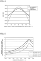
- FIG. 4 illustrates gain characteristic curves in an H-plane (plane in Y-Z directions) of the antenna device for the vehicle.
- FIG. 5 illustrates gain characteristic curves in the H-plane with a conductor length of a pair of parasitic elements varied.
- FIG. 6 is a diagram tabulating relative values of half-power angle in the H-plane with the conductor length of the pair of parasitic elements varied.
- FIG. 7 A is a diagram tabulating maximum radiation directions in the H-plane when a conductor length of a second parasitic element is made longer than that of a first parasitic element.
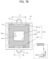
- FIG. 7 B is an internal configuration diagram of the antenna device for the vehicle, illustrating conductor lengths.
- FIG. 8 is a diagram explaining a wiring direction of a coaxial cable in a modification.
- FIG. 9 is a diagram illustrating a modification in which top faces of a pair of parasitic elements and a top face of a radiating element are set to different heights.
- FIG. 10 illustrates gain characteristic curves with a top-face height difference h varied.
- FIG. 11 is a diagram illustrating a modification in which a pair of parasitic elements is provided to outside a peripheral edge of a radiating element.
- directions are defined as follows.
- a radiating element 31 and ground plate 33 also referred to as a ground conductor plate
- the direction from the dielectric substrate 32 to the radiating element 31 is referred to as a “radiation direction.”
- the radiation direction has a fixed orientation rather than including both the direction from the dielectric substrate 32 to the radiating element 31 and the direction from the radiating element 31 to the dielectric substrate 32 .
- three orthogonal axes in a left-handed system are defined. A coordinate origin of the three orthogonal axes is set at the plate center of the radiating element 31 .
- reference directions parallel to each direction of the three orthogonal axes are added in each drawing.
- the term “reference directions” is used here because, correctly speaking, the origin of the three orthogonal axes is the plate center of the radiating element 31 .
- the reference directions are shown for reference purposes only.
- the direction perpendicular to the plate surface of the radiating element 31 is defined as a Z-axis direction and the orientation of the radiation direction is defined as a Z-axis positive direction.
- the direction along the direction of a line segment connecting the center of the radiating element 31 and a feeding point (also referred to as a core wire attachment hole) 31 h is defined as an X-axis direction (see FIG. 2 ) and the direction from the center of the radiating element 31 to the feeding point 31 h is defined as an X-axis positive direction.
- the Y-axis direction and Y-axis positive direction are self-evident because it is known that the three orthogonal axes in the left-handed system are used and because the X-axis positive direction and Z-axis positive direction have been defined.
- the directions are defined in other words, as viewed from the center (origin of the three orthogonal axes) of the radiating element 31 , the direction at an angle of elevation of 90 degrees with respect to the directions (plate directions) along the plate surface of the radiating element 31 is the Z-axis positive direction, the direction from the center of the radiating element 31 to the feeding point 31 h is the X-axis positive direction, and the orientation of the 3 o'clock direction is the Y-axis positive direction when the X-axis positive direction is the 12 o'clock direction.
- the plate directions of the radiating element 31 may be also called azimuth directions or bearing directions.
- X-axis direction herein means directions parallel to the X axis and includes both the X-axis positive (+) direction and X-axis negative ( ⁇ ) direction. The same applies to the Y-axis direction and Z-axis direction. Thus, each axis direction corresponds to the reference directions shown in each drawing.
- an E-plane and H-plane which are an electric field plane of the radiating element 31 and magnetic field plane, respectively, when viewed from the center (origin of the three orthogonal axes) of the radiating element 31 , a plane in X-Z directions including the X-axis direction and Z-axis direction is the E-plane while a plane in the Y-Z directions including the Y-axis direction and Z-axis direction is the H-plane.
- a plane including the direction perpendicular to the plate surface of the radiating element 31 and the direction of the line connecting the center of the radiating element 31 and feeding point 31 h is the E-plane while a plane perpendicular to the E-plane and including the direction perpendicular to the plate surface of the radiating element 31 is the H-plane.
- FIG. 1 is an external perspective view illustrating a configuration example of an antenna device for a vehicle 10 according to the present embodiment and a conceptual diagram illustrating an application example.
- the antenna device for the vehicle 10 which is equipped with a patch antenna for 5.9-GHz V2X (Vehicle-to-everything; Vehicle-to-Vehicle. Road-to-Vehicle etc.) communications, is installed in a predetermined orientation at a predetermined position of a vehicle 3 and connected to a V2X controller 5 via a coaxial cable 4 .
- V2X Vehicle-to-Vehicle. Road-to-Vehicle etc.
- the antenna device for the vehicle 10 is installed in upper part (e.g., near a rearview mirror) of a windshield inside the vehicle in such a way that the radiation direction (Z-axis positive direction) will face forward of the vehicle, i.e., in a traveling direction of the vehicle 3 , that the Y-axis positive direction will face to the right of the traveling direction of the vehicle 3 , and that the Y-axis negative direction will face to the left of the traveling direction of the vehicle 3 .
- the installation positions and installed number of the antenna devices for the vehicle 10 can be changed as appropriate according to environmental conditions of expected communications targets and the like.
- the antenna device for the vehicle 10 may be installed, for example, in two or more locations. Examples of possible installation locations include upper part of a dashboard, a bumper, a number plate mount, and pillars such as A-pillars.
- the antenna device for the vehicle 10 may be set up on rear glass inside the vehicle in such a way that the radiation direction will face rearward of the vehicle 3 , where the term “rearward” means the direction opposite to the traveling direction of the vehicle 3 .
- the antenna device for the vehicle 10 may be set up such that the radiation direction will face the right or left side of the vehicle 3 , where the term “right side” means the right side with respect to the traveling direction of the vehicle 3 and the term “left side” means the left side with respect to the traveling direction of the vehicle 3 . Also, if the antenna device for the vehicle 10 is structured to meet performance conditions of water resistance and dust resistance, the antenna device 10 may be installed on a roof of the vehicle 3 .
- the antenna device for the vehicle 10 has a quadrangular external appearance and contains the patch antenna 20 in a case having a split structure divided into a first housing 11 and second housing 12 in the radiation direction. Then, as on-vehicle mounting supports 13 provided on side faces of the housings are mounted on the vehicle 3 , the patch antenna 20 functions suitably as a vertically polarized antenna.
- the supports 13 are provided as bosses for use to insert bolts or screws for use to install the antenna device for the vehicle 10 , on both left and right side faces (opposite side faces in the Y-axis direction) of the housings as viewed from the vehicle 3 , but the setup positions of the supports 13 and the number of supports 13 to be set up may be selected as appropriate.
- the method for installing and fixing the antenna device for the vehicle 10 is not limited to the one that uses bolts or screws, and another method may be used, and accordingly, a structure such as a clip-on structure suitable for the method may be adopted for the supports 13 as appropriate.
- the supports 13 support the first housing 11 and second housing 12 such that the first housing 11 and second housing 12 will be installed in predetermined orientations at predetermined positions of the vehicle 3 .
- the supports 13 support the patch antenna 20 such that the patch antenna 20 will function as a vertically polarized antenna.
- FIG. 2 is a diagram explaining an internal configuration example of the antenna device for the vehicle 10 , illustrating the inside of the second housing 12 as viewed from the Z-axis positive direction with the first housing 11 removed.
- FIG. 3 is a diagram explaining an internal configuration example of the antenna device for the vehicle 10 similarly, and is also a longitudinal sectional view of the antenna device for the vehicle 10 , including the first housing 11 , taken along line III-III in FIG. 2 .
- the first housing 11 defines an upper accommodation space 11 a , which is a recess
- the second housing 12 defines a lower accommodation space 12 a , which is a recess.
- the upper accommodation space 11 a and lower accommodation space 12 a become a single continuous accommodation space when the first housing 11 and second housing 12 are assembled together.
- the patch antenna 20 is installed so as to fit in the accommodation space, and mainly in the lower accommodation space 12 a.
- the patch antenna 20 includes an antenna main body 30 and a pair of parasitic elements 40 ( 40 - 1 and 40 - 2 ).
- the antenna main body 30 has, for example, a quadrangular outer shape as viewed from the Z-axis positive direction and includes the radiating element 31 , the dielectric substrate 32 , and the ground plate 33 in this order from the top in FIG. 3 .
- the antenna main body 30 can be created by the application of a manufacturing method for printed circuit boards.
- the radiating element 31 has a quadrangular plate shape when viewed from the Z-axis positive direction and has a core wire attachment hole 31 h at a position offset (shifted) from the plate center in the X-axis positive direction (direction along a polarization plane of linearly polarized waves of the patch antenna 20 ), where the core wire attachment hole 31 h is a through-hole running in the Z-axis direction and used to insert and fix a core wire 41 of the coaxial cable 4 .
- the core wire attachment hole 31 h serves as a feeding point.
- the feeding point will be referred to as the feeding point 31 h using the same reference sign, as appropriate.
- the radiating element 31 is square in shape when viewed from the Z-axis positive direction, and is designed such that each of its sides is 13.5 mm long.
- the radiating element 31 and ground plate 33 are illustrated with intentionally increased thickness in the Z-axis direction, but actually these components may be formed as thin, plate-like films.
- the dielectric substrate 32 has a wider area than the radiating element 31 when viewed from the Z-axis positive direction. Besides, the dielectric substrate 32 has a non-illustrated core wire insertion hole that is configured to penetrate the dielectric substrate 32 in the Z-axis direction and positioned in such a way as to be communicated with the core wire attachment hole 31 h in the radiating element 31 during assembly.
- the ground plate 33 has a shape that is the same as or slightly smaller than an undersurface of the dielectric substrate 32 and has a non-illustrated core wire insertion hole that is communicated with the core wire attachment hole 31 h in the radiating element 31 and a core wire insertion hole in the dielectric substrate 32 during assembly.
- a coaxial substrate connector 22 is mounted on an undersurface of the ground plate 33 through a non-illustrated insertion hole provided in a bottom portion of the second housing 12 in such a way as to be coaxial with the core wire insertion hole in the ground plate 33 .
- the pair of parasitic elements 40 ( 40 - 1 and 40 - 2 ) is rodlike plate conductors (metal plates) when viewed from the Z-axis positive direction.
- the pair of parasitic elements 40 is provided at positions on opposite sides of the radiating element 31 by being spaced a predetermined distance b away from the opposite sides of the radiating element 31 in planar view in which the radiating element 31 is seen from the direction perpendicular to the plate surface of the radiating element 31 (in planar view in which the radiating element 31 is seen from the Z-axis positive direction). If the parasitic elements 40 are not spaced away from the radiating element 31 , the parasitic elements 40 would operate as if they were part of the radiating element 31 , which might result in changes in the frequency obtained by the patch antenna 20 .
- the pair of parasitic elements 40 - 1 and 40 - 2 is placed at positions on opposite sides of a line segment connecting the center of the radiating element 31 and feeding point 31 h , with respective longitudinal directions of the parasitic elements 40 - 1 and 40 - 2 being orientated along the direction of the line segment (X-axis direction) when viewed from the Z-axis positive direction.
- one of the pair of parasitic elements 40 - 1 and 40 - 2 e.g., the one on the lower side of FIG.
- the parasitic element 40 - 1 will also be referred to as a first parasitic element 40 - 1 as appropriate, and the other parasitic element 40 - 2 (the one on the upper side of FIG. 2 , i.e., on the side of the Y-axis positive direction) will also be referred to as a second parasitic element 40 - 2 as appropriate.
- the antenna main body 30 is fixed to the bottom portion of the second housing 12 . More specifically, a protrusion 12 t protruding in the Z-axis positive direction is provided on the bottom portion of the second housing 12 .
- the antenna main body 30 and the protrusion 12 t are fixed together, with the undersurface (end face on the side of the Z-axis negative direction) of the ground plate 33 abutting against a tip of the protrusion 12 t .
- Any fixing method can be selected as appropriate, including, for example, a method of bonding together the ground plate 33 and protrusion 12 t .
- spacing between the second housing 12 and antenna main body 30 may be an air layer (space), or a resin layer, which is an electrically insulative material.
- space space
- resin layer which is an electrically insulative material.
- the spacing is a resin layer, the resin can be used both as a space filler and bonding agent.
- a maximum length of a diagonal line of the radiating element 31 as viewed from the Z-axis positive direction will be referred to as a “maximum radiating element length” and denoted by “ ⁇ ” as illustrated in FIG. 2 .
- the radiating element 31 since the radiating element 31 has a square shape, of which each side is 13.5 mm long, the maximum radiating element length ⁇ is 19.1 mm.
- the conductor lengths of the parasitic elements 40 - 1 and 40 - 2 (i.e., the longitudinal lengths of the parasitic elements 40 - 1 and 40 - 2 ) and the distance b between the radiating element 31 and parasitic elements 40 - 1 and 40 - 2 are expressed as a magnification of the maximum radiating element length ⁇ and the actual length is shown in parentheses just behind the maximum radiating element length ⁇ . For example, if the conductor length is given as 0.86 ⁇ (approximately 16.5 mm), the length in question is 0.86 ⁇ times the maximum radiating element length ⁇ of 19.1 mm, and approximately 16.5 mm in the parentheses is the actual length.
- FIG. 4 illustrates gain characteristic curves in the H-plane (plane in Y-Z directions), and antenna gain with the Y-axis positive direction in the H-plane being set to 0 degrees and the Y-axis negative direction being set to 180 degrees.
- the 90-degree direction coincides with the Z-axis positive direction and corresponds to the direction at an angle of elevation of 90 degrees as viewed from the center of the radiating element 31 .
- the solid line represents antenna gain characteristics of the patch antenna 20 according to the present embodiment in a configuration in which the conductor lengths of the parasitic elements 40 - 1 and 40 - 2 are set to 0.86 ⁇ (approximately 16.5 mm) and the distance b is set to 0.25 ⁇ (approximately 4.75 mm).
- the broken line represents antenna gain characteristics of a comparative configuration corresponding to a conventional technique in which the pair of parasitic elements 40 - 1 and 40 - 2 is omitted.
- FIG. 5 illustrates gain characteristic curves obtained by graphically plotting minimum values of gain in low-elevation directions in the H-plane (in the ranges of 0 to 45 degrees and 135 to 180 degrees with the Y-axis positive direction in the H-plane being set to 0 degrees and the Y-axis negative direction being set to 180 degrees) when the conductor length of the pair of parasitic elements 40 - 1 and 40 - 2 is varied, where the gain characteristic curves obtained by varying the conductor length and using different distances b are represented by different line styles.
- the solid line is a gain characteristic curve obtained when the distance b is set to 0.51 ⁇ (approximately 9.75 mm)
- the chain line is a gain characteristic curve obtained when the distance b is set to 0.38 ⁇ (approximately 7.25 mm)
- the chain double-dashed line is a gain characteristic curve obtained when the distance b is set to 0.25 ⁇ (approximately 4.75 mm).
- FIG. 6 is a diagram tabulating relative values of half-power angle in the H-plane by varying the conductor length of the pair of parasitic elements 40 - 1 and 40 - 2 with the distance b set to 4.75 mm.
- “No conductor” in the topmost row of the conductor length column corresponds to the comparative configuration in which the pair of parasitic elements 40 - 1 and 40 - 2 is omitted and indicates the relative value (relative value of half-power angle) when the half-power angle of the comparative configuration is set to “1.000.”
- the conductor lengths of the pair of parasitic elements 40 - 1 and 40 - 2 are increased, the minimum values of gain in low-elevation directions increase as well. Then, peaks are reached when the conductor lengths are around 0.89 ⁇ (approximately 17.0 mm), and after the peaks, the minimum values of gain show a downward trend. However, with increases in the conductor lengths, the patch antenna 20 increases in size accordingly.
- the conductor lengths are 0.89 ⁇ (approximately 17.0 mm) or less, which is 0.89 times or less the maximum length ⁇ of the radiating element.
- the conductor length is 0.52 ⁇ (approximately 9.99 mm) or above, which is 0.52 times or more than the maximum length ⁇ of the radiating element.
- the distance b in FIG. 5 when attention is focused on the distance b in FIG. 5 , as the distance b is set to 0.25 ⁇ (approximately 4.75 mm), to 0.38 ⁇ (approximately 7.25 mm), and to 0.51 ⁇ (approximately 9.75 mm) in this order, the minimum values of gain in low-elevation directions increase as well.
- the gain increase range from the gain at a distance b of 0.38 ⁇ (approximately 7.25 mm) to the gain at a distance b of 0.51 ⁇ (approximately 9.75 mm) is smaller than the gain increase range from the gain at a distance b of 0.25 ⁇ (approximately 4.75 mm) to the gain at a distance b of 0.38 ⁇ (approximately 7.25 mm). Therefore, it is expected that after the distance b is increased to a certain level, the gain no longer increases greatly. Besides, with increases in the distance b, the patch antenna 20 increases in size accordingly.
- the distance b is 0.51 ⁇ (approximately 9.75 mm) or less, which is 0.51 times or less the maximum length ⁇ of the radiating element.
- FIG. 7 A is a diagram tabulating maximum radiation directions in the H-plane when a conductor length d of the second parasitic element 40 - 2 is fixed and a conductor length c of the first parasitic element 40 - 1 is varied.
- FIG. 7 B is an internal configuration diagram of an antenna device for the vehicle 10 equivalent to the one illustrated in FIG. 2 , illustrating the conductor length c of the first parasitic element 40 - 1 and the conductor length d of the second parasitic element 40 - 2 .
- FIG. 7 A is a diagram tabulating maximum radiation directions in the H-plane when a conductor length d of the second parasitic element 40 - 2 is fixed and a conductor length c of the first parasitic element 40 - 1 is varied.
- FIG. 7 B is an internal configuration diagram of an antenna device for the vehicle 10 equivalent to the one illustrated in FIG. 2 , illustrating the conductor length c of the first parasitic element 40 - 1 and the conductor length d of the second parasitic element 40
- “No conductor” in the topmost row of the conductor length c column corresponds to a configuration in which only the second parasitic element 40 - 2 is placed without the first parasitic element 40 - 1 .
- the maximum radiation directions correspond to azimuths in the H-plane, which is a plane in Y-Z directions when the Z-axis positive direction corresponding to the direction at an angle of elevation of 90 degrees as viewed from the center of the radiating element 31 is set to 0 degrees and the Y-axis positive direction is set to 90 degrees.
- the maximum radiation direction changes. Specifically, when the conductor length c is increased gradually from 6 mm with the conductor length d fixed, the azimuth of the maximum radiation direction gradually approaches 0 degrees. Then, although not illustrated, as the conductor length c is increased to the same length as the conductor length d, the azimuth of the maximum radiation direction becomes 0 degrees.
- the patch antenna 20 by configuring the patch antenna 20 by changing the conductor lengths c and d, it is possible to alter the maximum radiation direction.
- One of the reasons why the alteration is necessary is installation environment of the antenna device for the vehicle 10 .
- a wiring direction of a coaxial cable may be limited on account of layout and the like in the vehicle.
- available configurations are not limited to the one in which the coaxial cable 4 is wired by being inserted perpendicularly to the plate surface of the radiating element 31 as illustrated in FIG. 3 , and as illustrated in FIG. 8 , by adopting a connector whose wiring direction runs along the plate surface of the radiating element 31 , a coaxial cable 4 a is sometimes wired in parallel to the plate surface.
- the wiring direction affects radiation characteristics of radio waves, which could cause the maximum radiation direction to shift from the direction (e.g., the forward direction of the vehicle 3 ) expected at the time of installation.
- the respective conductor lengths of the parasitic elements 40 - 1 and 40 - 2 are set appropriately by taking into consideration the influence of the wiring configuration of the patch antenna 20 on the radiation characteristics of radio waves, it is possible to make an alteration during installation of the antenna device for the vehicle 10 on the vehicle 3 such that the maximum radiation direction will match a desired radiation direction. Also, even when a desired radiation direction is shifted from the forward direction of the vehicle as with, for example, an electronic toll collection system (ETC) antenna, if the respective conductor lengths of the parasitic elements 40 - 1 and 40 - 2 are changed according to the radiation direction, the antenna can be applied similarly.
- ETC electronic toll collection system
- the conductor length of at least one of the parasitic elements 40 - 1 and 40 - 2 is 0.89 ⁇ (approximately 17.0 mm) or less, which is 0.89 times or less than the maximum length ⁇ of the radiating element. More suitably both the parasitic elements satisfy this condition. Furthermore, it is sufficient that the distance b of at least one of the parasitic elements 40 - 1 and 40 - 2 is 0.51 ⁇ (approximately 9.75 mm) or less, which is 0.51 times or less than the maximum length ⁇ of the radiating element. More suitably both the parasitic elements satisfy this condition.
- the pair of parasitic elements 40 - 1 and 40 - 2 is provided on the peripheral edges of the top face of the dielectric substrate 32 such that the top faces of the parasitic elements 40 - 1 and 40 - 2 will be flush with the top face of the radiating element 31 .
- the pair of parasitic elements 40 - 1 and 40 - 2 may be provided such that the top faces thereof will differ in height from the top face of the radiating element 31 .
- FIG. 9 illustrates an example in which the top faces of the parasitic elements 40 - 1 and 40 - 2 are set higher than that of the radiating element 31 .
- Hp denotes the height of the top face of the parasitic elements 40 - 1 and 40 - 2
- Hr denotes the height of the top face of the radiating element 31
- the top-face height difference h is given by Hp ⁇ Hr.
- Hp and Hr are heights with respect to the top face of the dielectric substrate 32 .
- FIG. 10 illustrates gain characteristic curves of gain vs. azimuth in the H-plane (plane in Y-Z directions) with the Y-axis positive direction being set to 0 degrees and the Y-axis negative direction being set to 180 degrees, where the gain characteristic curves obtained by varying the top-face height difference h are represented by different line styles.
- the conductor lengths c and d of the parasitic elements 40 - 1 and 40 - 2 are 0.86 ⁇ (approximately 16.5 mm) and the distance b is 0.25 ⁇ (approximately 4.75 mm).
- the difference between the top-face height Hp of the parasitic elements 40 a - 1 and 40 a - 2 and the top-face height Hr of the radiating element 31 is 0 mm ⁇ Hp ⁇ Hr.
- the difference between the top-face height Hp of the parasitic elements 40 a - 1 and 40 a - 2 and the top-face height Hr of the radiating element 31 satisfies Hp ⁇ Hr ⁇ 0.05 ⁇ .
- Hp ⁇ Hr ⁇ 0.05 ⁇ desirably 0 mm ⁇ Hp ⁇ Hr. It is sufficient that the top-face height Hp of at least one of the pair of parasitic elements 40 - 1 and 40 - 2 satisfies 0 mm ⁇ Hp ⁇ Hr ⁇ 0.05 ⁇ . More suitably both the parasitic elements satisfy this condition.
- the outer shape of the antenna main body 30 as viewed from the Z-axis positive direction is not limited to the quadrangular shape illustrated by example in FIG. 2 , and may be a circular or other shape.
- the outer shape of the radiating element 31 as viewed from the Z-axis positive direction is not limited to the quadrangular shape illustrated by example in FIG. 2 , and may be a circular or other shape. Since the maximum length ⁇ of the radiating element as viewed from the Z-axis positive direction is the maximum length of the diagonal line, when the outer shape of the radiating element 31 as viewed from the Z-axis positive direction is circular, the maximum length ⁇ of the radiating element is the maximum length of a diameter of the radiating element 31 .
- any one of the pair of parasitic elements 40 - 1 and 40 - 2 may be orientated along the direction of a line segment (X-axis direction) connecting the center of the radiating element 31 and feeding point 31 h when viewed from the Z-axis positive direction. More suitably both the parasitic elements satisfy this condition.
- a pair of parasitic elements 40 b - 1 and 40 b - 2 may be provided to outside the peripheral edges of the radiating element 31 as flat-plate portions or thin-film portions parallel or substantially parallel to each other.
- the parasitic elements 40 b - 1 and 40 b - 2 may be placed by being pasted to an inner surface of the second housing 12 .
- the pair of parasitic elements 40 b - 1 and 40 b - 2 has a quadrangular flat-plate or thin-film shape and are placed on opposite sides of a line segment connecting the center of the radiating element 31 and feeding point 31 h and on opposite sides of the antenna main body 30 in such a way that the longitudinal direction will be orientated along the X-axis direction (direction of a line segment connecting the center of the radiating element 31 and feeding point 31 h ).
- the patch antenna 20 equipped with the pair of parasitic elements 40 ( 40 - 1 and 40 - 2 ) has been illustrated by example, the patch antenna 20 may be equipped with one parasitic element.
- the patch antenna 20 may be equipped with any one of the parasitic elements 40 - 1 and 40 - 2 .
- the shape of the parasitic elements as viewed from the Z-axis positive direction is not limited to the rodlike shape (rectangular shape, to be exact) illustrated by example in the above embodiment, and may be a quadrangular shape such as a rectangular shape whose shorter length as viewed from the Z-axis positive direction is increased, a polygonal shape, a circular shape, an elliptical shape, or the like.
- the present embodiment and modifications thereof can improve the gain in low-elevation directions as viewed from the center of the radiating element.
- materials for the dielectric substrate 32 in addition to commonly-used ceramics, inexpensive materials such as glass are available for use.
- available materials for the dielectric substrate 32 include glass epoxy resin substrates designated by the National Electrical Manufacturers Association (NEMA) symbol FR-4, paper phenol substrates designated by the NEMA symbol XPC, paper epoxy substrates designated by the NEMA symbol FR-3, and glass composite substrates designated by the NEMA symbol CEM-3 as well as glass polyimide substrates, fluorine (ceramic) substrates, and glass PPO substrates. Then, selecting an appropriate one of these materials according to cost and performance requirements, it is possible to obtain a suitable patch antenna.
- NEMA National Electrical Manufacturers Association
- the shape of the radiating element not only a polygonal shape such as a quadrangular shape, but also a polygonal shape whose corners have been cut off, a circular shape, an elliptical shape, or the like in planar view in which the radiating element is seen from the direction perpendicular to the plate surface of the radiating element can be adopted.
Landscapes
- Engineering & Computer Science (AREA)
- Remote Sensing (AREA)
- Waveguide Aerials (AREA)
- Aerials With Secondary Devices (AREA)
- Details Of Aerials (AREA)
- Support Of Aerials (AREA)
Applications Claiming Priority (3)
| Application Number | Priority Date | Filing Date | Title |
|---|---|---|---|
| JP2018-030681 | 2018-02-23 | ||
| JP2018030681 | 2018-02-23 | ||
| PCT/JP2019/004333 WO2019163521A1 (ja) | 2018-02-23 | 2019-02-07 | パッチアンテナおよび車載用アンテナ装置 |
Related Parent Applications (1)
| Application Number | Title | Priority Date | Filing Date |
|---|---|---|---|
| PCT/JP2019/004333 A-371-Of-International WO2019163521A1 (ja) | 2018-02-23 | 2019-02-07 | パッチアンテナおよび車載用アンテナ装置 |
Related Child Applications (1)
| Application Number | Title | Priority Date | Filing Date |
|---|---|---|---|
| US18/241,250 Continuation US12355156B2 (en) | 2018-02-23 | 2023-09-01 | Patch antenna and antenna device for vehicle |
Publications (2)
| Publication Number | Publication Date |
|---|---|
| US20210091480A1 US20210091480A1 (en) | 2021-03-25 |
| US11799208B2 true US11799208B2 (en) | 2023-10-24 |
Family
ID=67688072
Family Applications (2)
| Application Number | Title | Priority Date | Filing Date |
|---|---|---|---|
| US16/971,690 Active US11799208B2 (en) | 2018-02-23 | 2019-02-07 | Patch antenna and antenna device for vehicle |
| US18/241,250 Active 2039-02-28 US12355156B2 (en) | 2018-02-23 | 2023-09-01 | Patch antenna and antenna device for vehicle |
Family Applications After (1)
| Application Number | Title | Priority Date | Filing Date |
|---|---|---|---|
| US18/241,250 Active 2039-02-28 US12355156B2 (en) | 2018-02-23 | 2023-09-01 | Patch antenna and antenna device for vehicle |
Country Status (5)
| Country | Link |
|---|---|
| US (2) | US11799208B2 (https=) |
| EP (1) | EP3758147B1 (https=) |
| JP (3) | JP7231608B2 (https=) |
| CN (1) | CN111788741B (https=) |
| WO (1) | WO2019163521A1 (https=) |
Families Citing this family (8)
| Publication number | Priority date | Publication date | Assignee | Title |
|---|---|---|---|---|
| CN112005435B (zh) | 2018-04-24 | 2022-08-05 | Agc株式会社 | 车辆用天线、附带车辆用天线的窗玻璃及天线系统 |
| WO2021006033A1 (ja) * | 2019-07-11 | 2021-01-14 | 株式会社オートネットワーク技術研究所 | ルーフパネルモジュール及びルーフ用モジュール |
| WO2021065818A1 (ja) * | 2019-10-02 | 2021-04-08 | パナソニックIpマネジメント株式会社 | アンテナ装置及び車両 |
| JP7643450B2 (ja) * | 2020-03-24 | 2025-03-11 | Agc株式会社 | 車両用アンテナシステム |
| JP7490070B2 (ja) * | 2020-09-28 | 2024-05-24 | 株式会社ヨコオ | パッチアンテナ |
| CN112086745A (zh) * | 2020-09-30 | 2020-12-15 | 广州市埃特斯通讯设备有限公司 | 一种与v2x设备融合的etc天线 |
| WO2023100908A1 (ja) | 2021-12-03 | 2023-06-08 | Agc株式会社 | アンテナ装置及び車両用アンテナ装置 |
| WO2023127765A1 (ja) * | 2021-12-28 | 2023-07-06 | Agc株式会社 | アンテナ装置及び車両用アンテナ装置 |
Citations (11)
| Publication number | Priority date | Publication date | Assignee | Title |
|---|---|---|---|---|
| JPH0270104A (ja) | 1988-06-14 | 1990-03-09 | Koden Electron Co Ltd | 広指向性マイクロストリップアンテナ |
| JPH05183327A (ja) | 1991-12-26 | 1993-07-23 | Maspro Denkoh Corp | 車載用アンテナ |
| US5576718A (en) * | 1992-05-05 | 1996-11-19 | Aerospatiale Societe Nationale Industrielle | Thin broadband microstrip array antenna having active and parasitic patches |
| JP2002158534A (ja) | 2000-11-17 | 2002-05-31 | Ntt Docomo Inc | パッチ型アンテナ |
| JP2003347838A (ja) | 2002-05-30 | 2003-12-05 | Yokowo Co Ltd | アンテナ装置 |
| US20080088510A1 (en) * | 2004-09-30 | 2008-04-17 | Toto Ltd. | Microstrip Antenna And High Frequency Sensor Using Microstrip Antenna |
| US20080180332A1 (en) | 2007-01-25 | 2008-07-31 | Junichi Noro | Antenna device |
| US20080316110A1 (en) | 2007-06-22 | 2008-12-25 | Suncall Corporation | Patch Antenna and RFID Inlet |
| US20150097738A1 (en) | 2013-10-07 | 2015-04-09 | Denso Corporation | Antenna system and antenna unit |
| US20150123838A1 (en) * | 2013-11-06 | 2015-05-07 | Delphi Technologies, Inc. | Radar antenna assembly |
| JP2016171439A (ja) | 2015-03-12 | 2016-09-23 | 三菱電機株式会社 | アンテナ装置 |
Family Cites Families (14)
| Publication number | Priority date | Publication date | Assignee | Title |
|---|---|---|---|---|
| US6320544B1 (en) * | 2000-04-06 | 2001-11-20 | Lucent Technologies Inc. | Method of producing desired beam widths for antennas and antenna arrays in single or dual polarization |
| JP4541595B2 (ja) * | 2001-06-18 | 2010-09-08 | マスプロ電工株式会社 | マイクロストリップアンテナ |
| JP4098659B2 (ja) * | 2003-04-14 | 2008-06-11 | 三菱電機株式会社 | 狭域通信車載器 |
| US7505002B2 (en) * | 2006-12-04 | 2009-03-17 | Agc Automotive Americas R&D, Inc. | Beam tilting patch antenna using higher order resonance mode |
| DE102008000502A1 (de) * | 2008-03-04 | 2009-09-10 | Robert Bosch Gmbh | Radarsensor mit Patch-Antenne für Kraftfahrzeuge |
| JP4562010B2 (ja) * | 2008-06-04 | 2010-10-13 | ミツミ電機株式会社 | アンテナ素子 |
| JP2011055419A (ja) * | 2009-09-04 | 2011-03-17 | Japan Radio Co Ltd | 強結合素子アレーアンテナ |
| JP5554352B2 (ja) * | 2012-02-16 | 2014-07-23 | 古河電気工業株式会社 | 広角アンテナ及びアレーアンテナ |
| US9231306B2 (en) * | 2012-09-20 | 2016-01-05 | Casio Computer Co., Ltd. | Patch antenna and wireless communications device |
| US9806422B2 (en) * | 2013-09-11 | 2017-10-31 | International Business Machines Corporation | Antenna-in-package structures with broadside and end-fire radiations |
| CN203942014U (zh) * | 2014-05-12 | 2014-11-12 | 成都振芯科技股份有限公司 | 寄生电容加载实现的小型化天线 |
| JP6299505B2 (ja) * | 2014-07-23 | 2018-03-28 | 株式会社Soken | アンテナ装置 |
| JP6647121B2 (ja) * | 2016-04-05 | 2020-02-14 | 株式会社ユーシン | アンテナ装置、レーダ装置および無線通信装置 |
| US10594036B2 (en) * | 2017-07-06 | 2020-03-17 | Panasonic Intellectual Property Management Co., Ltd. | Antenna and vehicle |
-
2019
- 2019-02-07 US US16/971,690 patent/US11799208B2/en active Active
- 2019-02-07 JP JP2020501656A patent/JP7231608B2/ja active Active
- 2019-02-07 EP EP19756804.1A patent/EP3758147B1/en active Active
- 2019-02-07 WO PCT/JP2019/004333 patent/WO2019163521A1/ja not_active Ceased
- 2019-02-07 CN CN201980014484.6A patent/CN111788741B/zh active Active
-
2023
- 2023-02-16 JP JP2023022193A patent/JP7634032B2/ja active Active
- 2023-09-01 US US18/241,250 patent/US12355156B2/en active Active
-
2025
- 2025-02-07 JP JP2025019453A patent/JP2025065397A/ja active Pending
Patent Citations (14)
| Publication number | Priority date | Publication date | Assignee | Title |
|---|---|---|---|---|
| JPH0270104A (ja) | 1988-06-14 | 1990-03-09 | Koden Electron Co Ltd | 広指向性マイクロストリップアンテナ |
| JPH05183327A (ja) | 1991-12-26 | 1993-07-23 | Maspro Denkoh Corp | 車載用アンテナ |
| US5576718A (en) * | 1992-05-05 | 1996-11-19 | Aerospatiale Societe Nationale Industrielle | Thin broadband microstrip array antenna having active and parasitic patches |
| JP2002158534A (ja) | 2000-11-17 | 2002-05-31 | Ntt Docomo Inc | パッチ型アンテナ |
| JP2003347838A (ja) | 2002-05-30 | 2003-12-05 | Yokowo Co Ltd | アンテナ装置 |
| US7773035B2 (en) | 2004-09-30 | 2010-08-10 | Toto Ltd. | Microstrip antenna and high frequency sensor using microstrip antenna |
| US20080088510A1 (en) * | 2004-09-30 | 2008-04-17 | Toto Ltd. | Microstrip Antenna And High Frequency Sensor Using Microstrip Antenna |
| US20080180332A1 (en) | 2007-01-25 | 2008-07-31 | Junichi Noro | Antenna device |
| JP2008182523A (ja) | 2007-01-25 | 2008-08-07 | Mitsumi Electric Co Ltd | アンテナ装置 |
| US20080316110A1 (en) | 2007-06-22 | 2008-12-25 | Suncall Corporation | Patch Antenna and RFID Inlet |
| US20150097738A1 (en) | 2013-10-07 | 2015-04-09 | Denso Corporation | Antenna system and antenna unit |
| JP2015097377A (ja) | 2013-10-07 | 2015-05-21 | 株式会社日本自動車部品総合研究所 | アンテナシステムおよびアンテナユニット |
| US20150123838A1 (en) * | 2013-11-06 | 2015-05-07 | Delphi Technologies, Inc. | Radar antenna assembly |
| JP2016171439A (ja) | 2015-03-12 | 2016-09-23 | 三菱電機株式会社 | アンテナ装置 |
Non-Patent Citations (5)
| Title |
|---|
| European Patent Office dated Feb. 6, 2023 in corresponding European Patent Application No. 19756804.1, 7 pages. |
| Extended European search report dated Oct. 22, 2021, in corresponding European patent Application No. 19756804.1, 10 pages. |
| International Search Report and Written Opinion of the International Searching Authority dated Apr. 23, 2019, in corresponding PCT Application No. PCT/JP2019/004333 filed on Feb. 7, 2019, 10 pages. |
| Japanese Office Action dated Nov. 8, 2022 in corresponding Japanese Patent Application No. 2020-501656 (with machine-generated English translation), 8 pages. |
| Office Action dated Aug. 16, 2022, in corresponding Japanese patent Application No. 2020-501656, 10 pages. |
Also Published As
| Publication number | Publication date |
|---|---|
| JP7231608B2 (ja) | 2023-03-01 |
| JP2025065397A (ja) | 2025-04-17 |
| EP3758147A1 (en) | 2020-12-30 |
| JP7634032B2 (ja) | 2025-02-20 |
| EP3758147B1 (en) | 2024-06-12 |
| US12355156B2 (en) | 2025-07-08 |
| CN111788741A (zh) | 2020-10-16 |
| WO2019163521A1 (ja) | 2019-08-29 |
| CN111788741B (zh) | 2024-04-16 |
| EP3758147A4 (en) | 2021-11-24 |
| JP2023053368A (ja) | 2023-04-12 |
| US20210091480A1 (en) | 2021-03-25 |
| JPWO2019163521A1 (ja) | 2021-02-04 |
| US20230411865A1 (en) | 2023-12-21 |
Similar Documents
| Publication | Publication Date | Title |
|---|---|---|
| US12355156B2 (en) | Patch antenna and antenna device for vehicle | |
| US11476565B2 (en) | Patch antenna and antenna device for vehicle | |
| CN112310620B (zh) | 层叠贴片天线 | |
| US11005182B2 (en) | Patch antenna | |
| US12451606B2 (en) | Patch antenna | |
| US10720691B2 (en) | Film antenna and antenna device | |
| CN116636088A (zh) | 贴片天线及车载用天线装置 | |
| CN111602292A (zh) | 天线装置 | |
| CN112054291A (zh) | 天线装置 | |
| US20250087900A1 (en) | Antenna device | |
| EP4092827A1 (en) | Multiband antenna | |
| WO2022181576A1 (ja) | パッチアンテナ | |
| US11978970B2 (en) | Antenna device | |
| US20250141110A1 (en) | Antenna device | |
| JP7807432B2 (ja) | アンテナ装置 | |
| KR20130048893A (ko) | 차량용 파노라마 글래스 루프 안테나 장치 | |
| US20240322435A1 (en) | Antenna device and vehicle antenna device | |
| US12620713B2 (en) | Patch antenna and antenna device | |
| CN218160806U (zh) | 贴片天线以及天线装置 | |
| WO2025192069A1 (ja) | アンテナ装置 | |
| WO2025191968A1 (ja) | アンテナ及びアンテナ装置 | |
| WO2024034680A1 (ja) | パッチアンテナ | |
| WO2024116430A1 (ja) | アンテナ装置 | |
| WO2024010006A1 (ja) | アンテナ及び車両用アンテナ装置 |
Legal Events
| Date | Code | Title | Description |
|---|---|---|---|
| AS | Assignment |
Owner name: YOKOWO CO., LTD., JAPAN Free format text: ASSIGNMENT OF ASSIGNORS INTEREST;ASSIGNOR:SAMPO, TAKESHI;REEL/FRAME:053558/0993 Effective date: 20200818 |
|
| FEPP | Fee payment procedure |
Free format text: ENTITY STATUS SET TO UNDISCOUNTED (ORIGINAL EVENT CODE: BIG.); ENTITY STATUS OF PATENT OWNER: LARGE ENTITY |
|
| STPP | Information on status: patent application and granting procedure in general |
Free format text: DOCKETED NEW CASE - READY FOR EXAMINATION |
|
| STPP | Information on status: patent application and granting procedure in general |
Free format text: NON FINAL ACTION MAILED |
|
| STPP | Information on status: patent application and granting procedure in general |
Free format text: RESPONSE TO NON-FINAL OFFICE ACTION ENTERED AND FORWARDED TO EXAMINER |
|
| STPP | Information on status: patent application and granting procedure in general |
Free format text: FINAL REJECTION MAILED |
|
| STPP | Information on status: patent application and granting procedure in general |
Free format text: DOCKETED NEW CASE - READY FOR EXAMINATION |
|
| STPP | Information on status: patent application and granting procedure in general |
Free format text: NON FINAL ACTION MAILED |
|
| STPP | Information on status: patent application and granting procedure in general |
Free format text: RESPONSE TO NON-FINAL OFFICE ACTION ENTERED AND FORWARDED TO EXAMINER |
|
| STPP | Information on status: patent application and granting procedure in general |
Free format text: NOTICE OF ALLOWANCE MAILED -- APPLICATION RECEIVED IN OFFICE OF PUBLICATIONS |
|
| STPP | Information on status: patent application and granting procedure in general |
Free format text: PUBLICATIONS -- ISSUE FEE PAYMENT VERIFIED |
|
| STCF | Information on status: patent grant |
Free format text: PATENTED CASE |