US11621269B2 - Multi-level ferroelectric memory cell - Google Patents
Multi-level ferroelectric memory cell Download PDFInfo
- Publication number
- US11621269B2 US11621269B2 US16/298,413 US201916298413A US11621269B2 US 11621269 B2 US11621269 B2 US 11621269B2 US 201916298413 A US201916298413 A US 201916298413A US 11621269 B2 US11621269 B2 US 11621269B2
- Authority
- US
- United States
- Prior art keywords
- tapered
- electrode
- metal
- trench
- ferroelectric
- Prior art date
- Legal status (The legal status is an assumption and is not a legal conclusion. Google has not performed a legal analysis and makes no representation as to the accuracy of the status listed.)
- Active
Links
Images


Classifications
-
- H01L27/11514—
-
- G—PHYSICS
- G11—INFORMATION STORAGE
- G11C—STATIC STORES
- G11C11/00—Digital stores characterised by the use of particular electric or magnetic storage elements; Storage elements therefor
- G11C11/21—Digital stores characterised by the use of particular electric or magnetic storage elements; Storage elements therefor using electric elements
- G11C11/22—Digital stores characterised by the use of particular electric or magnetic storage elements; Storage elements therefor using electric elements using ferroelectric elements
- G11C11/221—Digital stores characterised by the use of particular electric or magnetic storage elements; Storage elements therefor using electric elements using ferroelectric elements using ferroelectric capacitors
-
- G—PHYSICS
- G11—INFORMATION STORAGE
- G11C—STATIC STORES
- G11C5/00—Details of stores covered by group G11C11/00
- G11C5/02—Disposition of storage elements, e.g. in the form of a matrix array
-
- H—ELECTRICITY
- H01—ELECTRIC ELEMENTS
- H01L—SEMICONDUCTOR DEVICES NOT COVERED BY CLASS H10
- H01L23/00—Details of semiconductor or other solid state devices
- H01L23/52—Arrangements for conducting electric current within the device in operation from one component to another, i.e. interconnections, e.g. wires, lead frames
- H01L23/522—Arrangements for conducting electric current within the device in operation from one component to another, i.e. interconnections, e.g. wires, lead frames including external interconnections consisting of a multilayer structure of conductive and insulating layers inseparably formed on the semiconductor body
- H01L23/5226—Via connections in a multilevel interconnection structure
-
- H01L27/11502—
-
- H—ELECTRICITY
- H01—ELECTRIC ELEMENTS
- H01L—SEMICONDUCTOR DEVICES NOT COVERED BY CLASS H10
- H01L28/00—Passive two-terminal components without a potential-jump or surface barrier for integrated circuits; Details thereof; Multistep manufacturing processes therefor
- H01L28/40—Capacitors
-
- H—ELECTRICITY
- H01—ELECTRIC ELEMENTS
- H01L—SEMICONDUCTOR DEVICES NOT COVERED BY CLASS H10
- H01L28/00—Passive two-terminal components without a potential-jump or surface barrier for integrated circuits; Details thereof; Multistep manufacturing processes therefor
- H01L28/40—Capacitors
- H01L28/55—Capacitors with a dielectric comprising a perovskite structure material
-
- H—ELECTRICITY
- H10—SEMICONDUCTOR DEVICES; ELECTRIC SOLID-STATE DEVICES NOT OTHERWISE PROVIDED FOR
- H10B—ELECTRONIC MEMORY DEVICES
- H10B53/00—Ferroelectric RAM [FeRAM] devices comprising ferroelectric memory capacitors
-
- H—ELECTRICITY
- H10—SEMICONDUCTOR DEVICES; ELECTRIC SOLID-STATE DEVICES NOT OTHERWISE PROVIDED FOR
- H10B—ELECTRONIC MEMORY DEVICES
- H10B53/00—Ferroelectric RAM [FeRAM] devices comprising ferroelectric memory capacitors
- H10B53/20—Ferroelectric RAM [FeRAM] devices comprising ferroelectric memory capacitors characterised by the three-dimensional arrangements, e.g. with cells on different height levels
-
- H—ELECTRICITY
- H01—ELECTRIC ELEMENTS
- H01L—SEMICONDUCTOR DEVICES NOT COVERED BY CLASS H10
- H01L28/00—Passive two-terminal components without a potential-jump or surface barrier for integrated circuits; Details thereof; Multistep manufacturing processes therefor
- H01L28/40—Capacitors
- H01L28/60—Electrodes
- H01L28/82—Electrodes with an enlarged surface, e.g. formed by texturisation
- H01L28/90—Electrodes with an enlarged surface, e.g. formed by texturisation having vertical extensions
-
- H—ELECTRICITY
- H10—SEMICONDUCTOR DEVICES; ELECTRIC SOLID-STATE DEVICES NOT OTHERWISE PROVIDED FOR
- H10B—ELECTRONIC MEMORY DEVICES
- H10B53/00—Ferroelectric RAM [FeRAM] devices comprising ferroelectric memory capacitors
- H10B53/10—Ferroelectric RAM [FeRAM] devices comprising ferroelectric memory capacitors characterised by the top-view layout
Definitions
- the present disclosure relates to semiconductor structures and, more particularly, to a multi-level ferroelectric memory cell and methods of manufacture.
- Ferroelectric RAM is a competitive memory technology with a large range of applications.
- Ferroelectric RAM (FeRAM, F-RAM or FRAM) is a random-access memory similar to DRAM.
- FRAM a ferroelectric layer is used instead of a dielectric layer to achieve non-volatility.
- FeRAM is one of a growing number of alternative non-volatile random-access memory technologies that offer the same functionality as flash memory.
- FRAM technology is based on 2-states cell architecture and is therefore bound to the limit of conventional binary memory systems. That is FRAM is limited to a single storage state per device.
- a structure comprises: a first metallization feature; a tapered ferroelectric capacitor comprising a first electrode, a second electrode and ferroelectric material between the first electrode and the second electrode, the first electrode contacting the first metallization feature; and a second metallization feature contacting the second electrode.
- a multi-level FRAM cell comprises: an upper metal line and upper via; a lower metal line and lower via; and a tapered vertical ferroelectric capacitor with a first metal electrode connected to the upper via and a second metal electrode connected to the lower via.
- a method comprises: forming a lower metal line and a lower via in dielectric material; forming trenches in the dielectric material above the lower via; forming tapered metal spacers on sidewalls of the trenches, and in each trench, a first of the metal spacers connecting to the lower via; forming ferroelectric material between the metal spacers on the sidewalls of the trenches; and forming an upper level via and metal lines, with the upper level via connected to a second of the metal spacers.
- FIG. 1 A is a top view of a memory array composed of multi-level FRAM cells and respective fabrication processes in accordance with aspects of the present disclosure.
- FIG. 1 B is a cross-sectional view of the lower via and metal line of the memory cell along line A-A of FIG. 1 A .
- FIG. 1 C is a cross-sectional view of the lower via and metal line of the memory cell along line B-B of FIG. 1 A .
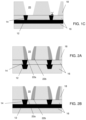
- FIGS. 2 A and 2 B are cross-sectional views along line A-A and line B-B, respectively, of electrode material formed on the sidewalls of trenches, amongst other features, and respective fabrication processes in accordance with aspect of the present disclosure.
- FIGS. 3 A and 3 B are cross-sectional views along line A-A and line B-B, respectively, of a ferroelectric material within the trenches, amongst other features, and respective fabrication processes in accordance with aspect of the present disclosure.
- FIGS. 4 A and 4 B are cross-sectional views along line A-A and line B-B, respectively, of an upper metallization feature directly contacting a second electrode of a tapered ferroelectric material capacitor, amongst other features, and respective fabrication processes in accordance with aspect of the present disclosure.
- FIG. 5 shows the fundamental operating principal of the tapered ferroelectric capacitor enabling multi-level storage in accordance with aspect of the present disclosure.
- FIG. 6 shows operating states of the tapered ferroelectric capacitor enabling multi-level storage in accordance with aspect of the present disclosure.
- FIG. 7 shows a chart of the different operating (polarization) states of the tapered ferroelectric capacitor enabling multi-level storage in accordance with aspect of the present disclosure.
- FIG. 8 shows an exemplary circuit used for the write operations of FIG. 7 .
- the present disclosure relates to semiconductor structures and, more particularly, to a multi-level ferroelectric memory cell and methods of manufacture. More specifically, the present disclosure is directed to an analogue ferroelectric memory cell using a tapered vertical ferroelectric capacitor capable of reaching different overall states of polarization within an electric field depending on an applied bitline voltage.
- the present disclosure provides a multi-level ferroelectric memory cell (FRAM) with the capacity to store multiple memory states with enhanced flexibility, new capabilities and reaching broader applications such as neuromorphic.
- the FRAM also exhibits short programming time, lower power usage and fast write performance.
- the memory cell comprises an upper metal line and via and a lower metal line and via.
- a tapered vertical ferroelectric capacitor is provided with one metal electrode connected to the upper via and metal line and the other metal electrode connected to the lower via and metal line. The use of the tapered vertical ferroelectric capacitor enables controllability to generate a continuous range of polarization states in the capacitor depending on the applied bitline voltage.
- the memory cell can be a sigmoid neuron memory cell.
- the method of forming the memory cell comprises: forming the lower metal line and lower via; forming trenches; forming an inner metal spacer inside the trenches, and in each trench, one metal spacer is connected to the lower via and the other spacer is not connected to the lower via; forming ferroelectric material between the metal spacers; and forming upper level via and metal lines in contact with the other metal spacer.
- the ferroelectric material and the metal spacers form a tapered ferroelectric capacitor.
- the multi-level ferroelectric memory cell of the present disclosure can be manufactured in a number of ways using a number of different tools.
- the methodologies and tools are used to form structures with dimensions in the micrometer and nanometer scale.
- the methodologies, i.e., technologies, employed to manufacture the multi-level ferroelectric memory cell of the present disclosure have been adopted from integrated circuit (IC) technology.
- IC integrated circuit
- the structures are built on wafers and are realized in films of material patterned by photolithographic processes on the top of a wafer.
- the fabrication of the multi-level ferroelectric memory cell uses three basic building blocks: (i) deposition of thin films of material on a substrate, (ii) applying a patterned mask on top of the films by photolithographic imaging, and (iii) etching the films selectively to the mask.
- FIG. 1 A is a top view of a memory array composed of multi-level FRAM cell and respective fabrication processes in accordance with aspects of the present disclosure.
- FIG. 1 B is a cross-sectional view of the lower via and metal line of the memory cell along line A-A of FIG. 1 A ; whereas, FIG. 1 C is a cross-sectional view of the lower via and metal line of the memory cell along line B-B of FIG. 1 A .
- the memory array 10 is formed by a periodic arrangement in both X and Y directions of multiple memory cells 10 ′ (as shown in FIG. 1 A ).
- the memory array 10 includes multiple lower metal lines 12 (Y-lines) and lower vias 14 formed in an insulator material (interlevel dielectric material) 16 .
- the insulator material 16 can be an oxide based material, e.g., SiO 2 .
- the metal line 12 and the lower vias 14 can be any appropriate conductive material, e.g., metal material or metal alloy, known to those of ordinary skill in the art.
- the memory array 10 also includes multiple upper metal lines (X-lines) and upper vias (as shown in FIG. 1 A ).
- the metal line 12 and the lower vias 14 can be fabricated using conventional lithography, etching and deposition processes.
- a resist formed over the insulator material 16 is exposed to energy (light) to form a pattern (opening).
- An etching process with a selective chemistry e.g., reactive ion etching (RIE)
- RIE reactive ion etching
- the resist can then be removed by a conventional oxygen ashing process or other known stripants.
- the conductive material (appropriate metal material or metal alloy) can be deposited by any conventional deposition processes, e.g., chemical vapor deposition (CVD) processes. Any residual material on the surface of the insulator material 16 can be removed by conventional chemical mechanical polishing (CMP) processes.
- CMP chemical mechanical polishing
- the metal line 14 can be formed in a similar manner (additive process) or through a subtractive process.
- additional insulator material 18 is deposited over the lower vias 14 .
- a plurality of trenches 20 is formed in the insulator material 18 , slightly offset from each of the lower vias 14 .
- the distance of the offset “x” would be approximately equal to a thickness of electrode material subsequently deposited on the sidewall of the trenches 20 (e.g., tapered trenches).
- the trenches 20 are formed by conventional lithography and etching processes known to those of skill in the art such that no further explanation is required herein.
- FIGS. 2 A and 2 B are respective cross-sectional views of electrode material formed on the sidewalls of trenches and respective fabrication processes in accordance with aspect of the present disclosure.
- electrode material is formed on the sidewalls of the trenches 20 to form a first electrode 22 a and a second electrode 22 b (of a capacitor) on the sidewalls of the trenches 20 . Due to the tapered nature of the trenches 20 , the first electrode 22 a and the second electrode 22 b can be non-parallel electrodes. As shown in these figures, the first electrode 22 a will directly contact the lower vias 14 , whereas, the second electrode 22 b is remote (offset) from the lower vias 14 .
- the electrode material can be TiN, copper, aluminum, tungsten or other appropriate conductive material matching the ferroelectric material operating requirement.
- the electrode material which form first electrode 22 a and the second electrode 22 b is deposited by a conformal deposition of metal material without pinch-off in the trench 20 .
- An anisotropic metal RIE will be used to taper the metal material on the first electrode 22 a and the second electrode 22 b (liner) in the via sidewalls. In this way, as shown in the figures, the thickness of the metal material at the top is thinner than the bottom of the via 20 .
- the electrode material can be formed on the sidewalls of the trenches 20 by a conformal deposition process, e.g., CVD, followed by an anisotropic etching process to remove the electrode material from horizontal surfaces of the insulator material 16 , 18 .
- the anisotropic etching process tapers the first electrode 22 a and the second electrode 22 b , with a narrow section at an upper portion of the trenches 20 and a wider section at the lower portion of the trenches 20 .
- the taper can form a rounded or curved vertical side surface.
- the tapering of the electrodes 22 a , 22 b can be adjusted during the anisotropic RIE process to tune the capacitor parameters, hence providing flexibility to meet multi-level FRAM design requirements.
- FIGS. 3 A and 3 B are respective cross-sectional views of a ferroelectric material within the trenches and respective fabrication processes in accordance with aspect of the present disclosure. More specifically, in FIGS. 3 A and 3 B , a ferroelectric material 24 is deposited into the remaining portion of the trenches 20 between the first electrode 22 a and the second electrode 22 b .
- examples of the ferroelectric material include, but are not limited to: doped-Hafnium Oxide or other doped high-k dielectric materials, e.g., ZrO 2 :HfO 2 , Y:HfO 2 , Si:HfO 2 , Al:HfO 2 , La:HfO 2 , etc., as well as complex oxides with Perovskite crystalline structures, e.g. Pb(Zr,Ti)O 3 , BiFeO 3 , BaTiO 3 , etc.
- doped-Hafnium Oxide or other doped high-k dielectric materials e.g., ZrO 2 :HfO 2 , Y:HfO 2 , Si:HfO 2 , Al:HfO 2 , La:HfO 2 , etc.
- complex oxides with Perovskite crystalline structures e.g. Pb(Zr,Ti)O 3 , BiFeO 3 ,
- the ferroelectric material 24 will have a tapered profile or shape, with a narrower section at a lower portion of the trenches 20 and a wider section at the upper portion of the trenches 20 .
- the ferroelectric material 24 will act as an insulator material between the two electrodes 22 a , 22 b , forming a capacitor with one of the electrodes 22 a contacting the lower vias 14 and another of the electrodes 22 b contacting upper wiring features (as shown in FIGS. 4 A and 4 B ).
- the ferroelectric material 24 can be deposited by a conventional deposition process included CVD, atomic layer deposition (ALD) or plasma vapor deposition (PVD), to name a few. Following the deposition process, the ferroelectric material 24 will undergo a planarization process, e.g., chemical mechanical polishing (CMP). The planarization process can also remove a portion of the upper section of the electrodes 22 a , 22 b.
- CVD atomic layer deposition
- PVD plasma vapor deposition
- CMP chemical mechanical polishing
- the ferroelectric material provides advantages over other insulator materials. For example, upon the application of an electric field, a spontaneous electric polarization inherent to the crystal structure of the ferroelectric material exists, which will not disappear even when the electric field is removed.
- an applied external electric field will move the center atom in the direction of the electric field, which will remain in such state even after the field is removed. The position of the “central” atom affects the voltage which is used to determine whether it represents “0” or “1”.
- FIGS. 4 A and 4 B are respective cross-sectional views of an upper metallization feature directly contacting the second electrode of the tapered ferroelectric material capacitor, amongst other features, and respective fabrication processes. More specifically, as shown in FIGS. 4 A and 4 B , an upper metallization feature is formed in direct contact with the second electrode 22 b (and remote or away from the first electrode 22 a ). In embodiments, the upper metallization feature includes an upper via 26 and an upper metal line 28 . As shown in these figures, the second electrode 22 b is directly contacting the upper via 26 .
- a tapered profile ferroelectric material capacitor with two non-parallel electrodes e.g., first electrode 22 a and second electrode 22 b
- a lower metallization feature e.g., lower via 12 and lower metal line 14
- the upper metallization feature e.g., upper via 26 and upper metal line 28 .
- FIG. 5 shows the fundamental operating principal of the tapered ferroelectric capacitor 100 enabling multi-level storage.
- the tapered ferroelectric material capacitor 100 exhibits the following characteristics:
- E x is the electric field seen by the ferroelectric material in vertical region x
- V Bit Line is the voltage applied on the ferroelectric material by the bitline and is a constant for a given programing state
- d x is the thickness of the ferroelectric in vertical region x.
- the electric field E x is dependent on the distance d x of the ferroelectric material between the electrodes 22 a , 22 b .
- the tapered ferroelectric capacitor 100 enables controllability to generate a continuous range of polarization states in the capacitor depending on the applied Bit line voltage. For neuromorphic applications, this can be used to create Resistive Synapses carrying multiple “weights” (e.g., multi-states), which will increase energy efficiency and density of neural networks. More specifically, in implementation, the tapered ferroelectric material capacitor can be used to form sigmoid neurons useful for deep learning.
- the ferroelectric material gets polarized for a given threshold electric field (E th ) which depends on the intrinsic physical properties of the ferroelectric material. If the electric field (E) applied across the ferroelectric material is above the threshold electric field (E th ) value, the ferroelectric material will get polarized along the applied field and the intrinsic electrical field in the ferroelectric material will remain once the applied electric field (E) is removed. On the other hand, if the electric field (E) applied across the ferroelectric material is below the threshold electric field (E th ) value, the ferroelectric material will not retain its internal polarization once the applied electric field (E) is removed.
- E th threshold electric field
- ferroelectric capacitor Since the ferroelectric capacitor is tapered: (i) one part of the ferroelectric material can experience an applied electric field (E) above the threshold electric field (E th ) value (bottom part of the capacitor which gets polarized), while (ii) the other part of the ferroelectric material experiences an applied electric field (E) below the threshold electric field (E th ) value (top part of the capacitor which does not get polarized).
- FIG. 6 shows different operating (polarization) states of the tapered ferroelectric capacitor enabling multi-level storage in accordance with aspect of the present disclosure. More specifically, FIG. 6 shows five different states (e.g., states, 0, 1, 2, 3, 4) of the multi-operational tapered ferroelectric material capacitor 100 ; although other states are contemplated herein depending on the applied bitline voltages.
- the different bitline voltages V BL for each of the operational states include: 0 ⁇ V 1 ⁇ V 2 ⁇ V 3 ⁇ V 4 .
- the polarization can be adjusted based on different applied bitline voltages, where the portion under the threshold electric field value (E th ) of the tapered ferroelectric capacitor 100 graphically represents a reverse polarization state.
- E th the portion under the threshold electric field value of the tapered ferroelectric capacitor 100 graphically represents a reverse polarization state.
- This same modeling can be used to create an FeRAM holding N number of memory states by adjusting the height and tapering of the vertical ferroelectric material capacitor.
- FIG. 7 shows a chart of the different operating (polarization) states of the tapered ferroelectric capacitor enabling multi-level storage in accordance with aspect of the present disclosure.
- the chart of FIG. 7 shows respective timing diagrams, polarization states and a state sequence of the ferroelectric capacitor described herein over five (5) write operations (i.e., write operations 0, 1, 2, 3, 4); although it should be understood that more or less states are contemplated herein.
- the timing diagrams show the bitline voltage being applied to a bitline, where V 0 ⁇ V 1 ⁇ V 2 ⁇ V 3 ⁇ V 4 .
- the polarization state schematically or graphically shows the polarization of the ferroelectric material capacitor during the application of each bitline voltage.
- the ferroelectric capacitor gets uniformly polarized in one direction (the capacitor is driven in only a single direction); whereas at V 1 at lower (narrower) portion of the ferroelectric capacitor is reverse polarized.
- the amount of reverse polarization also will increase, effectively allowing or storing of multiple memory states.
- the respective graphs sequentially show the state sequence (e.g., polarization) for the ferroelectric material capacitor during the application of each bitline voltage; that is, the graphs show that the polarization is driven to a different part of the cell due it tapered shape.
- FIG. 8 shows an exemplary schematic of a circuit used for the write operations described in FIG. 7 .
- the circuit 200 includes a wordline WL, a plateline PL and a bitline BL that intersects the wordline WL and the plateline PL.
- An access transistor 202 is connected to the wordline WL, with CBL representing a total parasitic capacitance of the bitline BL.
- the ferroelectric material capacitor 100 is in series with the access transistor 202 and the plateline PL. In embodiments, when the access transistor 202 is ON, the ferroelectric material capacitor 100 is connected to the bitline (BL) and can be written to or read by the plateline (PL).
- the read operation of the multi-state FRAM could be performed using a method similar to standard FRAM.
- the following illustrative steps can be used to for the read operation: 1) precharge the Bit line (BL) to 0 V; 2) activating the Word line (WL) establishes a capacitor divider between the Plateline (PL) and the ground; 3) depending on the data stored, the ferroelectric material capacitor 100 can be approximated by C 0 or C 1 and thus the voltage could be V 0 or V 1 ; 4) the Plateline (PL) is raised to V DD ; 5) at this point, the sense amplifier is activated to drive the Bitline (BL) (e.g., if the Bitline (BL) is V 1 , then full V DD ; if the Bitline (BL) is V 0 , then full 0 V); and 6) the Word line (WL) is kept activated until the sensed voltage on the Bitline (BL) restores the original data back into the memory cell.
- the Bitline (BL) e.g
- multiple states can be read using the total capacitance of the tapered ferroelectric material capacitor 100 .
- the ferroelectric material capacitor 100 can be approximated by C 0 , C 1 , C 2 , C 3 or C 4 and thus voltage could be V 0 , V 1 , V 2 , V 3 or V 4 .
- the read process would be destructive and rewriting the cell would be required after each read.
- the method(s) as described above is used in the fabrication of integrated circuit chips.
- the resulting integrated circuit chips can be distributed by the fabricator in raw wafer form (that is, as a single wafer that has multiple unpackaged chips), as a bare die, or in a packaged form.
- the chip is mounted in a single chip package (such as a plastic carrier, with leads that are affixed to a motherboard or other higher level carrier) or in a multichip package (such as a ceramic carrier that has either or both surface interconnections or buried interconnections).
- the chip is then integrated with other chips, discrete circuit elements, and/or other signal processing devices as part of either (a) an intermediate product, such as a motherboard, or (b) an end product.
- the end product can be any product that includes integrated circuit chips, ranging from toys and other low-end applications to advanced computer products having a display, a keyboard or other input device, and a central processor.
Landscapes
- Engineering & Computer Science (AREA)
- Power Engineering (AREA)
- Computer Hardware Design (AREA)
- Microelectronics & Electronic Packaging (AREA)
- Chemical & Material Sciences (AREA)
- Materials Engineering (AREA)
- Physics & Mathematics (AREA)
- Condensed Matter Physics & Semiconductors (AREA)
- General Physics & Mathematics (AREA)
- Semiconductor Memories (AREA)
- Static Random-Access Memory (AREA)
Priority Applications (4)
| Application Number | Priority Date | Filing Date | Title |
|---|---|---|---|
| US16/298,413 US11621269B2 (en) | 2019-03-11 | 2019-03-11 | Multi-level ferroelectric memory cell |
| TW109104095A TWI772744B (zh) | 2019-03-11 | 2020-02-10 | 多階鐵電記憶胞 |
| CN202010086592.9A CN111681692B (zh) | 2019-03-11 | 2020-02-11 | 多级铁电存储单元 |
| DE102020201684.4A DE102020201684B4 (de) | 2019-03-11 | 2020-02-11 | Mehrfachniveau-FRAM-Zelle und Herstellungsverfahren |
Applications Claiming Priority (1)
| Application Number | Priority Date | Filing Date | Title |
|---|---|---|---|
| US16/298,413 US11621269B2 (en) | 2019-03-11 | 2019-03-11 | Multi-level ferroelectric memory cell |
Publications (2)
| Publication Number | Publication Date |
|---|---|
| US20200295017A1 US20200295017A1 (en) | 2020-09-17 |
| US11621269B2 true US11621269B2 (en) | 2023-04-04 |
Family
ID=72241153
Family Applications (1)
| Application Number | Title | Priority Date | Filing Date |
|---|---|---|---|
| US16/298,413 Active US11621269B2 (en) | 2019-03-11 | 2019-03-11 | Multi-level ferroelectric memory cell |
Country Status (4)
| Country | Link |
|---|---|
| US (1) | US11621269B2 (de) |
| CN (1) | CN111681692B (de) |
| DE (1) | DE102020201684B4 (de) |
| TW (1) | TWI772744B (de) |
Families Citing this family (2)
| Publication number | Priority date | Publication date | Assignee | Title |
|---|---|---|---|---|
| JP2022051465A (ja) * | 2020-09-18 | 2022-03-31 | キオクシア株式会社 | 半導体記憶装置 |
| US11682618B2 (en) * | 2021-03-25 | 2023-06-20 | Taiwan Semiconductor Manufacturing Company, Ltd. | Hybrid metal line structure |
Citations (23)
| Publication number | Priority date | Publication date | Assignee | Title |
|---|---|---|---|---|
| US5155573A (en) * | 1989-12-25 | 1992-10-13 | Kabushiki Kaisha Toshiba | Ferroelectric capacitor and a semiconductor device having the same |
| US6281535B1 (en) * | 1999-01-22 | 2001-08-28 | Agilent Technologies, Inc. | Three-dimensional ferroelectric capacitor structure for nonvolatile random access memory cell |
| US20020155659A1 (en) * | 2001-04-23 | 2002-10-24 | Macronix International Co., Ltd. | Vertical ferroelectric capacitor |
| US20030043618A1 (en) * | 2001-09-04 | 2003-03-06 | Nec Corporation | Semiconductor memory device including shadow ram |
| US6624040B1 (en) * | 2002-09-20 | 2003-09-23 | Chartered Semiconductor Manufacturing Ltd. | Self-integrated vertical MIM capacitor in the dual damascene process |
| US20050067644A1 (en) * | 2003-09-30 | 2005-03-31 | Haoren Zhuang | Device and a method for forming a capacitor device |
| US20060038217A1 (en) * | 2004-08-20 | 2006-02-23 | Matsushita Electric Industrial Co., Ltd. | Dielectric memory device and method for fabricating the same |
| US20080079046A1 (en) * | 2006-09-28 | 2008-04-03 | Kabushiki Kaisha Toshiba | Semiconductor apparatus and method for manufacturing the same |
| US20090294906A1 (en) * | 2008-05-29 | 2009-12-03 | Rohm Co., Ltd. | Semiconductor device and fabrication method for the same, and light modulation device and fabrication method for the same |
| US20100163943A1 (en) * | 2008-09-24 | 2010-07-01 | Kabushiki Kaisha Toshiba | Semiconductor memory device |
| US20110001141A1 (en) * | 2004-06-24 | 2011-01-06 | Nec Corporation | Semiconductor device, Manufacturing method for the same, and electronic device |
| US20150027278A1 (en) | 2013-07-26 | 2015-01-29 | Tsan-Chang Lee | Open wrench |
| US9047568B1 (en) | 2012-09-20 | 2015-06-02 | Brain Corporation | Apparatus and methods for encoding of sensory data using artificial spiking neurons |
| US20150317557A1 (en) | 2014-05-01 | 2015-11-05 | Qualcomm Incorporated | Temporal spike encoding for temporal learning |
| US9195934B1 (en) | 2013-01-31 | 2015-11-24 | Brain Corporation | Spiking neuron classifier apparatus and methods using conditionally independent subsets |
| US9542644B2 (en) | 2013-08-13 | 2017-01-10 | Qualcomm Incorporated | Methods and apparatus for modulating the training of a neural device |
| US20170033120A1 (en) | 2015-07-30 | 2017-02-02 | Snu R&Db Foundation | Vertical neuromorphic devices stacked structure and array of the structure |
| US20170061278A1 (en) | 2015-08-31 | 2017-03-02 | SK Hynix Inc. | Synapse and neuromorphic device including the same |
| US9601546B1 (en) | 2016-09-12 | 2017-03-21 | International Business Machines Corporation | Scaled cross bar array with undercut electrode |
| US9773204B2 (en) | 2015-12-30 | 2017-09-26 | SK Hynix Inc. | Neuromorphic device including synapses having carrier traps distributed at multiple energy levels |
| US20180197879A1 (en) | 2016-02-26 | 2018-07-12 | SK Hynix Inc. | Multi-level ferroelectric memory device and method of manufacturing the same |
| WO2018194544A1 (en) | 2017-04-17 | 2018-10-25 | Intel Corporation | Multi-bit ferroelectric memory |
| US20200161250A1 (en) * | 2018-11-16 | 2020-05-21 | International Business Machines Corporation | Ild gap fill for memory device stack array |
Family Cites Families (9)
| Publication number | Priority date | Publication date | Assignee | Title |
|---|---|---|---|---|
| KR100279297B1 (ko) * | 1998-06-20 | 2001-02-01 | 윤종용 | 반도체 장치 및 그의 제조 방법 |
| US6368517B1 (en) * | 1999-02-17 | 2002-04-09 | Applied Materials, Inc. | Method for preventing corrosion of a dielectric material |
| US6690251B2 (en) * | 2001-04-11 | 2004-02-10 | Kyocera Wireless Corporation | Tunable ferro-electric filter |
| KR100500940B1 (ko) * | 2002-06-21 | 2005-07-14 | 주식회사 하이닉스반도체 | 반도체 장치의 캐패시터 제조방법 |
| CN101084580A (zh) * | 2003-12-22 | 2007-12-05 | 皇家飞利浦电子股份有限公司 | 非易失性铁电存储器设备的制备方法和由此获得的存储器设备 |
| KR100601953B1 (ko) * | 2004-05-03 | 2006-07-14 | 삼성전자주식회사 | 메모리 소자의 캐패시터 및 그 제조 방법 |
| CN106575702B (zh) * | 2014-08-19 | 2018-05-22 | 沙特基础工业全球技术公司 | 具有多级操作的非易失性铁电存储器单元 |
| US9159829B1 (en) * | 2014-10-07 | 2015-10-13 | Micron Technology, Inc. | Recessed transistors containing ferroelectric material |
| US9899073B2 (en) * | 2016-06-27 | 2018-02-20 | Micron Technology, Inc. | Multi-level storage in ferroelectric memory |
-
2019
- 2019-03-11 US US16/298,413 patent/US11621269B2/en active Active
-
2020
- 2020-02-10 TW TW109104095A patent/TWI772744B/zh active
- 2020-02-11 DE DE102020201684.4A patent/DE102020201684B4/de active Active
- 2020-02-11 CN CN202010086592.9A patent/CN111681692B/zh active Active
Patent Citations (23)
| Publication number | Priority date | Publication date | Assignee | Title |
|---|---|---|---|---|
| US5155573A (en) * | 1989-12-25 | 1992-10-13 | Kabushiki Kaisha Toshiba | Ferroelectric capacitor and a semiconductor device having the same |
| US6281535B1 (en) * | 1999-01-22 | 2001-08-28 | Agilent Technologies, Inc. | Three-dimensional ferroelectric capacitor structure for nonvolatile random access memory cell |
| US20020155659A1 (en) * | 2001-04-23 | 2002-10-24 | Macronix International Co., Ltd. | Vertical ferroelectric capacitor |
| US20030043618A1 (en) * | 2001-09-04 | 2003-03-06 | Nec Corporation | Semiconductor memory device including shadow ram |
| US6624040B1 (en) * | 2002-09-20 | 2003-09-23 | Chartered Semiconductor Manufacturing Ltd. | Self-integrated vertical MIM capacitor in the dual damascene process |
| US20050067644A1 (en) * | 2003-09-30 | 2005-03-31 | Haoren Zhuang | Device and a method for forming a capacitor device |
| US20110001141A1 (en) * | 2004-06-24 | 2011-01-06 | Nec Corporation | Semiconductor device, Manufacturing method for the same, and electronic device |
| US20060038217A1 (en) * | 2004-08-20 | 2006-02-23 | Matsushita Electric Industrial Co., Ltd. | Dielectric memory device and method for fabricating the same |
| US20080079046A1 (en) * | 2006-09-28 | 2008-04-03 | Kabushiki Kaisha Toshiba | Semiconductor apparatus and method for manufacturing the same |
| US20090294906A1 (en) * | 2008-05-29 | 2009-12-03 | Rohm Co., Ltd. | Semiconductor device and fabrication method for the same, and light modulation device and fabrication method for the same |
| US20100163943A1 (en) * | 2008-09-24 | 2010-07-01 | Kabushiki Kaisha Toshiba | Semiconductor memory device |
| US9047568B1 (en) | 2012-09-20 | 2015-06-02 | Brain Corporation | Apparatus and methods for encoding of sensory data using artificial spiking neurons |
| US9195934B1 (en) | 2013-01-31 | 2015-11-24 | Brain Corporation | Spiking neuron classifier apparatus and methods using conditionally independent subsets |
| US20150027278A1 (en) | 2013-07-26 | 2015-01-29 | Tsan-Chang Lee | Open wrench |
| US9542644B2 (en) | 2013-08-13 | 2017-01-10 | Qualcomm Incorporated | Methods and apparatus for modulating the training of a neural device |
| US20150317557A1 (en) | 2014-05-01 | 2015-11-05 | Qualcomm Incorporated | Temporal spike encoding for temporal learning |
| US20170033120A1 (en) | 2015-07-30 | 2017-02-02 | Snu R&Db Foundation | Vertical neuromorphic devices stacked structure and array of the structure |
| US20170061278A1 (en) | 2015-08-31 | 2017-03-02 | SK Hynix Inc. | Synapse and neuromorphic device including the same |
| US9773204B2 (en) | 2015-12-30 | 2017-09-26 | SK Hynix Inc. | Neuromorphic device including synapses having carrier traps distributed at multiple energy levels |
| US20180197879A1 (en) | 2016-02-26 | 2018-07-12 | SK Hynix Inc. | Multi-level ferroelectric memory device and method of manufacturing the same |
| US9601546B1 (en) | 2016-09-12 | 2017-03-21 | International Business Machines Corporation | Scaled cross bar array with undercut electrode |
| WO2018194544A1 (en) | 2017-04-17 | 2018-10-25 | Intel Corporation | Multi-bit ferroelectric memory |
| US20200161250A1 (en) * | 2018-11-16 | 2020-05-21 | International Business Machines Corporation | Ild gap fill for memory device stack array |
Non-Patent Citations (10)
| Title |
|---|
| Burr et al., "Neuromorphic computing using non-volatile memory", Advances in Physics: X, ISSN: (Print) 2374-6149 (Online) Journal homepage: http://www.tandfonline.com/loi/tapx20, Published Online: Dec. 4, 2016, vol. 2, No. 1, 37 pages. |
| German Office Action in related DE Application No. 109104095 dated Sep. 29, 2021, 11 pages. |
| Jerry et al., "A ferroelectric field effect transistor based synaptic weight cell", Journal of Physics D: Applied Physics, vol. 51, No. 43, Aug. 23, 2018, Abstract, 2 pages. |
| Jerry et al., "Ferroelectric FET analog synapse for acceleration of deep neural network training", IFFF International Electron Devices Meeting (IEDM), San Francisco, CA, 2017, 4 pages. |
| Ni et al., "In-Memory Computing Primitive for Sensor Data Fusion in 28 nm HKMG FeFET Technology", IEEE International Electron Devices Meeting (IEDM), San Francisco, CA, 2018, 4 pages. |
| Notice of Allowance in related Taiwanese Application No. 109104095 dated Jun. 14, 2022, 2 pages. |
| Taiwanese Office Action in related TW Application No. 109104095 dated Dec. 2, 2020, 13 pages. |
| Taiwanese Office Action in related TW Application No. 109104095 dated Jul. 6, 2021, 14 pages. |
| Wang et al., "Recent Advances on Neuromorphic Systems Using Phase-Change Materials", Nanoscale Research Letters 12:347, DOI 10.1186/s11671-017-2114-9, 2017, 22 pages. |
| Yoon et al., "A FeFET Based Processing-In-Memory Architecture for Solving Distributed Least-Square Optimizations", IEEE, 76th Device Research Conference (DRC), Santa Barbara, CA, 2018, 2 pages. |
Also Published As
| Publication number | Publication date |
|---|---|
| CN111681692B (zh) | 2023-08-29 |
| TW202034506A (zh) | 2020-09-16 |
| CN111681692A (zh) | 2020-09-18 |
| DE102020201684B4 (de) | 2022-06-09 |
| US20200295017A1 (en) | 2020-09-17 |
| DE102020201684A1 (de) | 2020-09-17 |
| TWI772744B (zh) | 2022-08-01 |
Similar Documents
| Publication | Publication Date | Title |
|---|---|---|
| US20240147738A1 (en) | Memory device and method of forming the same | |
| CN110024034B (zh) | 使用漏斗装置的单元干扰预防 | |
| US10692870B2 (en) | Three-dimensional devices having reduced contact length | |
| TWI654742B (zh) | 記憶胞及形成電容器之方法 | |
| US20180006044A1 (en) | Ferroelectric memory and methods of forming the same | |
| US8053302B2 (en) | Non-volatile memory device and method of manufacturing same | |
| US7297997B2 (en) | Semiconductor memory device with dual storage node and fabricating and operating methods thereof | |
| JP4708793B2 (ja) | Cu2sのmocvd形成 | |
| US11088170B2 (en) | Three-dimensional ferroelectric memory array including integrated gate selectors and methods of forming the same | |
| TWI686931B (zh) | 三維記憶體陣列及其形成方法 | |
| WO2022000486A1 (en) | Method for reading and writing memory cells in three-dimensional feram | |
| KR100687051B1 (ko) | 스택형 강유전체 메모리 장치, 그 제조 방법, 강유전체메모리 회로 및 구동 방법 | |
| US11621269B2 (en) | Multi-level ferroelectric memory cell | |
| US20220231026A1 (en) | Hybrid memory device and method of forming the same | |
| US6046927A (en) | Nonvolatile semiconductor memory device, a method of fabricating the same, and read, erase write methods of the same | |
| US9478461B2 (en) | Conductive line structure with openings | |
| Kim et al. | Future memory technology and ferroelectric memory as an ultimate memory solution | |
| WO2024103281A1 (en) | Three-dimensional ferroelectric field effect transistor random access memory devices and fabricating methods thereof | |
| US20230397432A1 (en) | Method device and electronic device including the same | |
| JP2024056635A (ja) | 非二元論理用の強誘電体ナノ粒子キャパシタ | |
| WO2004030069A2 (en) | Method of patterning capacitors and capacitors made thereby | |
| JPH11220105A (ja) | 強誘電体メモリ装置およびその製造方法 | |
| KR19980068061A (ko) | 강유전체 메모리 장치 제조 방법 |
Legal Events
| Date | Code | Title | Description |
|---|---|---|---|
| AS | Assignment |
Owner name: GLOBALFOUNDRIES INC., CAYMAN ISLANDS Free format text: ASSIGNMENT OF ASSIGNORS INTEREST;ASSIGNORS:FROUGIER, JULIEN;XIE, RUILONG;REEL/FRAME:048838/0592 Effective date: 20190308 |
|
| FEPP | Fee payment procedure |
Free format text: ENTITY STATUS SET TO UNDISCOUNTED (ORIGINAL EVENT CODE: BIG.); ENTITY STATUS OF PATENT OWNER: LARGE ENTITY |
|
| AS | Assignment |
Owner name: GLOBALFOUNDRIES U.S. INC., CALIFORNIA Free format text: ASSIGNMENT OF ASSIGNORS INTEREST;ASSIGNOR:GLOBALFOUNDRIES INC.;REEL/FRAME:054633/0001 Effective date: 20201022 |
|
| STPP | Information on status: patent application and granting procedure in general |
Free format text: RESPONSE TO NON-FINAL OFFICE ACTION ENTERED AND FORWARDED TO EXAMINER |
|
| STPP | Information on status: patent application and granting procedure in general |
Free format text: FINAL REJECTION MAILED |
|
| STPP | Information on status: patent application and granting procedure in general |
Free format text: RESPONSE AFTER FINAL ACTION FORWARDED TO EXAMINER |
|
| STPP | Information on status: patent application and granting procedure in general |
Free format text: ADVISORY ACTION MAILED |
|
| STPP | Information on status: patent application and granting procedure in general |
Free format text: DOCKETED NEW CASE - READY FOR EXAMINATION |
|
| STPP | Information on status: patent application and granting procedure in general |
Free format text: NON FINAL ACTION MAILED |
|
| AS | Assignment |
Owner name: GLOBALFOUNDRIES U.S. INC., NEW YORK Free format text: RELEASE BY SECURED PARTY;ASSIGNOR:WILMINGTON TRUST, NATIONAL ASSOCIATION;REEL/FRAME:056987/0001 Effective date: 20201117 |
|
| STPP | Information on status: patent application and granting procedure in general |
Free format text: RESPONSE TO NON-FINAL OFFICE ACTION ENTERED AND FORWARDED TO EXAMINER |
|
| STPP | Information on status: patent application and granting procedure in general |
Free format text: FINAL REJECTION MAILED |
|
| STPP | Information on status: patent application and granting procedure in general |
Free format text: RESPONSE AFTER FINAL ACTION FORWARDED TO EXAMINER |
|
| STPP | Information on status: patent application and granting procedure in general |
Free format text: ADVISORY ACTION MAILED |
|
| STPP | Information on status: patent application and granting procedure in general |
Free format text: DOCKETED NEW CASE - READY FOR EXAMINATION |
|
| STPP | Information on status: patent application and granting procedure in general |
Free format text: NON FINAL ACTION MAILED |
|
| STPP | Information on status: patent application and granting procedure in general |
Free format text: RESPONSE TO NON-FINAL OFFICE ACTION ENTERED AND FORWARDED TO EXAMINER |
|
| STPP | Information on status: patent application and granting procedure in general |
Free format text: NOTICE OF ALLOWANCE MAILED -- APPLICATION RECEIVED IN OFFICE OF PUBLICATIONS |
|
| STCF | Information on status: patent grant |
Free format text: PATENTED CASE |