US10934624B2 - Laminated film - Google Patents
Laminated film Download PDFInfo
- Publication number
- US10934624B2 US10934624B2 US15/773,499 US201615773499A US10934624B2 US 10934624 B2 US10934624 B2 US 10934624B2 US 201615773499 A US201615773499 A US 201615773499A US 10934624 B2 US10934624 B2 US 10934624B2
- Authority
- US
- United States
- Prior art keywords
- film
- thin film
- based thin
- gas
- silicon oxide
- Prior art date
- Legal status (The legal status is an assumption and is not a legal conclusion. Google has not performed a legal analysis and makes no representation as to the accuracy of the status listed.)
- Active
Links
- 239000010409 thin film Substances 0.000 claims abstract description 223
- 239000010408 film Substances 0.000 claims abstract description 168
- VYPSYNLAJGMNEJ-UHFFFAOYSA-N Silicium dioxide Chemical compound O=[Si]=O VYPSYNLAJGMNEJ-UHFFFAOYSA-N 0.000 claims abstract description 93
- 239000002985 plastic film Substances 0.000 claims abstract description 91
- 229920006255 plastic film Polymers 0.000 claims abstract description 91
- 229910052814 silicon oxide Inorganic materials 0.000 claims abstract description 91
- 229910003481 amorphous carbon Inorganic materials 0.000 claims abstract description 56
- 238000005268 plasma chemical vapour deposition Methods 0.000 claims abstract description 13
- 229920006284 nylon film Polymers 0.000 claims description 6
- 229920000728 polyester Polymers 0.000 claims description 3
- 230000004888 barrier function Effects 0.000 abstract description 26
- 238000004519 manufacturing process Methods 0.000 abstract description 26
- 239000011248 coating agent Substances 0.000 abstract description 22
- 238000000576 coating method Methods 0.000 abstract description 22
- 239000007789 gas Substances 0.000 description 144
- 239000007858 starting material Substances 0.000 description 72
- 239000000463 material Substances 0.000 description 47
- 239000004952 Polyamide Substances 0.000 description 36
- 229920002647 polyamide Polymers 0.000 description 36
- HSFWRNGVRCDJHI-UHFFFAOYSA-N alpha-acetylene Natural products C#C HSFWRNGVRCDJHI-UHFFFAOYSA-N 0.000 description 31
- 125000002534 ethynyl group Chemical group [H]C#C* 0.000 description 31
- 230000015572 biosynthetic process Effects 0.000 description 28
- PQDJYEQOELDLCP-UHFFFAOYSA-N trimethylsilane Chemical compound C[SiH](C)C PQDJYEQOELDLCP-UHFFFAOYSA-N 0.000 description 25
- 239000000203 mixture Substances 0.000 description 24
- IJGRMHOSHXDMSA-UHFFFAOYSA-N Atomic nitrogen Chemical compound N#N IJGRMHOSHXDMSA-UHFFFAOYSA-N 0.000 description 23
- 229910052799 carbon Inorganic materials 0.000 description 18
- 238000000034 method Methods 0.000 description 18
- OKTJSMMVPCPJKN-UHFFFAOYSA-N Carbon Chemical compound [C] OKTJSMMVPCPJKN-UHFFFAOYSA-N 0.000 description 17
- 229910044991 metal oxide Inorganic materials 0.000 description 16
- 150000004706 metal oxides Chemical class 0.000 description 16
- 238000001878 scanning electron micrograph Methods 0.000 description 16
- 230000000052 comparative effect Effects 0.000 description 12
- 239000011261 inert gas Substances 0.000 description 12
- 238000003475 lamination Methods 0.000 description 12
- 229920000139 polyethylene terephthalate Polymers 0.000 description 11
- 239000005020 polyethylene terephthalate Substances 0.000 description 11
- 238000002156 mixing Methods 0.000 description 10
- 229910052757 nitrogen Inorganic materials 0.000 description 10
- MYMOFIZGZYHOMD-UHFFFAOYSA-N Dioxygen Chemical compound O=O MYMOFIZGZYHOMD-UHFFFAOYSA-N 0.000 description 9
- 239000003085 diluting agent Substances 0.000 description 9
- 229910001882 dioxygen Inorganic materials 0.000 description 9
- 150000002736 metal compounds Chemical class 0.000 description 9
- 238000012545 processing Methods 0.000 description 9
- 229920005989 resin Polymers 0.000 description 9
- 239000011347 resin Substances 0.000 description 9
- UQEAIHBTYFGYIE-UHFFFAOYSA-N hexamethyldisiloxane Chemical compound C[Si](C)(C)O[Si](C)(C)C UQEAIHBTYFGYIE-UHFFFAOYSA-N 0.000 description 8
- 239000004215 Carbon black (E152) Substances 0.000 description 7
- QVGXLLKOCUKJST-UHFFFAOYSA-N atomic oxygen Chemical compound [O] QVGXLLKOCUKJST-UHFFFAOYSA-N 0.000 description 7
- 238000005452 bending Methods 0.000 description 7
- 229930195733 hydrocarbon Natural products 0.000 description 7
- 150000002430 hydrocarbons Chemical class 0.000 description 7
- 239000001301 oxygen Substances 0.000 description 7
- 229910052760 oxygen Inorganic materials 0.000 description 7
- 239000005022 packaging material Substances 0.000 description 7
- -1 polypropylene Polymers 0.000 description 7
- 230000000694 effects Effects 0.000 description 6
- VNWKTOKETHGBQD-UHFFFAOYSA-N methane Chemical compound C VNWKTOKETHGBQD-UHFFFAOYSA-N 0.000 description 6
- 238000005192 partition Methods 0.000 description 6
- PNEYBMLMFCGWSK-UHFFFAOYSA-N Alumina Chemical compound [O-2].[O-2].[O-2].[Al+3].[Al+3] PNEYBMLMFCGWSK-UHFFFAOYSA-N 0.000 description 5
- 238000001505 atmospheric-pressure chemical vapour deposition Methods 0.000 description 5
- XUIMIQQOPSSXEZ-UHFFFAOYSA-N Silicon Chemical compound [Si] XUIMIQQOPSSXEZ-UHFFFAOYSA-N 0.000 description 4
- BOTDANWDWHJENH-UHFFFAOYSA-N Tetraethyl orthosilicate Chemical compound CCO[Si](OCC)(OCC)OCC BOTDANWDWHJENH-UHFFFAOYSA-N 0.000 description 4
- OLBVUFHMDRJKTK-UHFFFAOYSA-N [N].[O] Chemical compound [N].[O] OLBVUFHMDRJKTK-UHFFFAOYSA-N 0.000 description 4
- 230000005540 biological transmission Effects 0.000 description 4
- 238000000151 deposition Methods 0.000 description 4
- 230000008021 deposition Effects 0.000 description 4
- 230000006872 improvement Effects 0.000 description 4
- 230000008569 process Effects 0.000 description 4
- 229910052710 silicon Inorganic materials 0.000 description 4
- 239000010703 silicon Substances 0.000 description 4
- 229920002379 silicone rubber Polymers 0.000 description 4
- 239000004945 silicone rubber Substances 0.000 description 4
- 238000003786 synthesis reaction Methods 0.000 description 4
- LFQCEHFDDXELDD-UHFFFAOYSA-N tetramethyl orthosilicate Chemical compound CO[Si](OC)(OC)OC LFQCEHFDDXELDD-UHFFFAOYSA-N 0.000 description 4
- 238000004804 winding Methods 0.000 description 4
- LYCAIKOWRPUZTN-UHFFFAOYSA-N Ethylene glycol Chemical compound OCCO LYCAIKOWRPUZTN-UHFFFAOYSA-N 0.000 description 3
- 238000007664 blowing Methods 0.000 description 3
- 238000010586 diagram Methods 0.000 description 3
- 229910001873 dinitrogen Inorganic materials 0.000 description 3
- 230000007246 mechanism Effects 0.000 description 3
- 229920003023 plastic Polymers 0.000 description 3
- 239000004033 plastic Substances 0.000 description 3
- 229920006267 polyester film Polymers 0.000 description 3
- 239000004953 Aliphatic polyamide Substances 0.000 description 2
- RYGMFSIKBFXOCR-UHFFFAOYSA-N Copper Chemical compound [Cu] RYGMFSIKBFXOCR-UHFFFAOYSA-N 0.000 description 2
- YCKRFDGAMUMZLT-UHFFFAOYSA-N Fluorine atom Chemical compound [F] YCKRFDGAMUMZLT-UHFFFAOYSA-N 0.000 description 2
- XEEYBQQBJWHFJM-UHFFFAOYSA-N Iron Chemical compound [Fe] XEEYBQQBJWHFJM-UHFFFAOYSA-N 0.000 description 2
- 239000004642 Polyimide Substances 0.000 description 2
- 239000004743 Polypropylene Substances 0.000 description 2
- ATUOYWHBWRKTHZ-UHFFFAOYSA-N Propane Chemical compound CCC ATUOYWHBWRKTHZ-UHFFFAOYSA-N 0.000 description 2
- 229920003231 aliphatic polyamide Polymers 0.000 description 2
- 239000004411 aluminium Substances 0.000 description 2
- XAGFODPZIPBFFR-UHFFFAOYSA-N aluminium Chemical group [Al] XAGFODPZIPBFFR-UHFFFAOYSA-N 0.000 description 2
- 229910052782 aluminium Inorganic materials 0.000 description 2
- 229910052802 copper Inorganic materials 0.000 description 2
- 239000010949 copper Substances 0.000 description 2
- 238000005336 cracking Methods 0.000 description 2
- 230000003247 decreasing effect Effects 0.000 description 2
- 239000003814 drug Substances 0.000 description 2
- 229920001971 elastomer Polymers 0.000 description 2
- 239000011737 fluorine Substances 0.000 description 2
- 229910052731 fluorine Inorganic materials 0.000 description 2
- 229910052739 hydrogen Inorganic materials 0.000 description 2
- 230000002452 interceptive effect Effects 0.000 description 2
- 238000010030 laminating Methods 0.000 description 2
- 238000005259 measurement Methods 0.000 description 2
- CMWTZPSULFXXJA-VIFPVBQESA-N naproxen Chemical group C1=C([C@H](C)C(O)=O)C=CC2=CC(OC)=CC=C21 CMWTZPSULFXXJA-VIFPVBQESA-N 0.000 description 2
- BASFCYQUMIYNBI-UHFFFAOYSA-N platinum Chemical compound [Pt] BASFCYQUMIYNBI-UHFFFAOYSA-N 0.000 description 2
- 229920001721 polyimide Polymers 0.000 description 2
- 239000002861 polymer material Substances 0.000 description 2
- 229920001155 polypropylene Polymers 0.000 description 2
- 238000007639 printing Methods 0.000 description 2
- 239000005060 rubber Substances 0.000 description 2
- 238000007789 sealing Methods 0.000 description 2
- OEPOKWHJYJXUGD-UHFFFAOYSA-N 2-(3-phenylmethoxyphenyl)-1,3-thiazole-4-carbaldehyde Chemical compound O=CC1=CSC(C=2C=C(OCC=3C=CC=CC=3)C=CC=2)=N1 OEPOKWHJYJXUGD-UHFFFAOYSA-N 0.000 description 1
- 229920001634 Copolyester Polymers 0.000 description 1
- OTMSDBZUPAUEDD-UHFFFAOYSA-N Ethane Chemical compound CC OTMSDBZUPAUEDD-UHFFFAOYSA-N 0.000 description 1
- LFQSCWFLJHTTHZ-UHFFFAOYSA-N Ethanol Chemical compound CCO LFQSCWFLJHTTHZ-UHFFFAOYSA-N 0.000 description 1
- 229920000219 Ethylene vinyl alcohol Polymers 0.000 description 1
- UFHFLCQGNIYNRP-UHFFFAOYSA-N Hydrogen Chemical compound [H][H] UFHFLCQGNIYNRP-UHFFFAOYSA-N 0.000 description 1
- JHWNWJKBPDFINM-UHFFFAOYSA-N Laurolactam Chemical compound O=C1CCCCCCCCCCCN1 JHWNWJKBPDFINM-UHFFFAOYSA-N 0.000 description 1
- OFOBLEOULBTSOW-UHFFFAOYSA-N Malonic acid Chemical compound OC(=O)CC(O)=O OFOBLEOULBTSOW-UHFFFAOYSA-N 0.000 description 1
- 229920000299 Nylon 12 Polymers 0.000 description 1
- 229920002292 Nylon 6 Polymers 0.000 description 1
- 229920002302 Nylon 6,6 Polymers 0.000 description 1
- BQCADISMDOOEFD-UHFFFAOYSA-N Silver Chemical compound [Ag] BQCADISMDOOEFD-UHFFFAOYSA-N 0.000 description 1
- ORLQHILJRHBSAY-UHFFFAOYSA-N [1-(hydroxymethyl)cyclohexyl]methanol Chemical compound OCC1(CO)CCCCC1 ORLQHILJRHBSAY-UHFFFAOYSA-N 0.000 description 1
- FDLQZKYLHJJBHD-UHFFFAOYSA-N [3-(aminomethyl)phenyl]methanamine Chemical compound NCC1=CC=CC(CN)=C1 FDLQZKYLHJJBHD-UHFFFAOYSA-N 0.000 description 1
- 238000010521 absorption reaction Methods 0.000 description 1
- 239000004760 aramid Substances 0.000 description 1
- 229920003235 aromatic polyamide Polymers 0.000 description 1
- 125000003118 aryl group Chemical group 0.000 description 1
- 230000008901 benefit Effects 0.000 description 1
- 239000011111 cardboard Substances 0.000 description 1
- 239000013626 chemical specie Substances 0.000 description 1
- 229910052681 coesite Inorganic materials 0.000 description 1
- 150000001875 compounds Chemical class 0.000 description 1
- 239000000470 constituent Substances 0.000 description 1
- 229920001577 copolymer Polymers 0.000 description 1
- 229910052906 cristobalite Inorganic materials 0.000 description 1
- 230000006866 deterioration Effects 0.000 description 1
- 238000002474 experimental method Methods 0.000 description 1
- 238000011049 filling Methods 0.000 description 1
- PCHJSUWPFVWCPO-UHFFFAOYSA-N gold Chemical compound [Au] PCHJSUWPFVWCPO-UHFFFAOYSA-N 0.000 description 1
- 229910052737 gold Inorganic materials 0.000 description 1
- 239000010931 gold Substances 0.000 description 1
- 239000001257 hydrogen Substances 0.000 description 1
- 125000004435 hydrogen atom Chemical group [H]* 0.000 description 1
- 238000007733 ion plating Methods 0.000 description 1
- 229910052742 iron Inorganic materials 0.000 description 1
- 229910052751 metal Inorganic materials 0.000 description 1
- 239000002184 metal Substances 0.000 description 1
- 239000007769 metal material Substances 0.000 description 1
- 238000012986 modification Methods 0.000 description 1
- 230000004048 modification Effects 0.000 description 1
- 239000012785 packaging film Substances 0.000 description 1
- 229920006280 packaging film Polymers 0.000 description 1
- 238000004806 packaging method and process Methods 0.000 description 1
- 239000011087 paperboard Substances 0.000 description 1
- NRNCYVBFPDDJNE-UHFFFAOYSA-N pemoline Chemical compound O1C(N)=NC(=O)C1C1=CC=CC=C1 NRNCYVBFPDDJNE-UHFFFAOYSA-N 0.000 description 1
- 238000005240 physical vapour deposition Methods 0.000 description 1
- 229910052697 platinum Inorganic materials 0.000 description 1
- 229920003207 poly(ethylene-2,6-naphthalate) Polymers 0.000 description 1
- 229920001707 polybutylene terephthalate Polymers 0.000 description 1
- 239000011112 polyethylene naphthalate Substances 0.000 description 1
- 229920000642 polymer Polymers 0.000 description 1
- 239000002243 precursor Substances 0.000 description 1
- 239000001294 propane Substances 0.000 description 1
- 238000004064 recycling Methods 0.000 description 1
- 230000009467 reduction Effects 0.000 description 1
- 150000003377 silicon compounds Chemical class 0.000 description 1
- 239000000377 silicon dioxide Substances 0.000 description 1
- LIVNPJMFVYWSIS-UHFFFAOYSA-N silicon monoxide Chemical compound [Si-]#[O+] LIVNPJMFVYWSIS-UHFFFAOYSA-N 0.000 description 1
- 229910052709 silver Inorganic materials 0.000 description 1
- 239000004332 silver Substances 0.000 description 1
- 238000001179 sorption measurement Methods 0.000 description 1
- 238000004544 sputter deposition Methods 0.000 description 1
- 229910001220 stainless steel Inorganic materials 0.000 description 1
- 239000010935 stainless steel Substances 0.000 description 1
- 229910052682 stishovite Inorganic materials 0.000 description 1
- 238000006467 substitution reaction Methods 0.000 description 1
- 230000001360 synchronised effect Effects 0.000 description 1
- 229910052905 tridymite Inorganic materials 0.000 description 1
- 238000001771 vacuum deposition Methods 0.000 description 1
Images


Classifications
-
- C—CHEMISTRY; METALLURGY
- C23—COATING METALLIC MATERIAL; COATING MATERIAL WITH METALLIC MATERIAL; CHEMICAL SURFACE TREATMENT; DIFFUSION TREATMENT OF METALLIC MATERIAL; COATING BY VACUUM EVAPORATION, BY SPUTTERING, BY ION IMPLANTATION OR BY CHEMICAL VAPOUR DEPOSITION, IN GENERAL; INHIBITING CORROSION OF METALLIC MATERIAL OR INCRUSTATION IN GENERAL
- C23C—COATING METALLIC MATERIAL; COATING MATERIAL WITH METALLIC MATERIAL; SURFACE TREATMENT OF METALLIC MATERIAL BY DIFFUSION INTO THE SURFACE, BY CHEMICAL CONVERSION OR SUBSTITUTION; COATING BY VACUUM EVAPORATION, BY SPUTTERING, BY ION IMPLANTATION OR BY CHEMICAL VAPOUR DEPOSITION, IN GENERAL
- C23C16/00—Chemical coating by decomposition of gaseous compounds, without leaving reaction products of surface material in the coating, i.e. chemical vapour deposition [CVD] processes
- C23C16/44—Chemical coating by decomposition of gaseous compounds, without leaving reaction products of surface material in the coating, i.e. chemical vapour deposition [CVD] processes characterised by the method of coating
- C23C16/54—Apparatus specially adapted for continuous coating
- C23C16/545—Apparatus specially adapted for continuous coating for coating elongated substrates
-
- C—CHEMISTRY; METALLURGY
- C23—COATING METALLIC MATERIAL; COATING MATERIAL WITH METALLIC MATERIAL; CHEMICAL SURFACE TREATMENT; DIFFUSION TREATMENT OF METALLIC MATERIAL; COATING BY VACUUM EVAPORATION, BY SPUTTERING, BY ION IMPLANTATION OR BY CHEMICAL VAPOUR DEPOSITION, IN GENERAL; INHIBITING CORROSION OF METALLIC MATERIAL OR INCRUSTATION IN GENERAL
- C23C—COATING METALLIC MATERIAL; COATING MATERIAL WITH METALLIC MATERIAL; SURFACE TREATMENT OF METALLIC MATERIAL BY DIFFUSION INTO THE SURFACE, BY CHEMICAL CONVERSION OR SUBSTITUTION; COATING BY VACUUM EVAPORATION, BY SPUTTERING, BY ION IMPLANTATION OR BY CHEMICAL VAPOUR DEPOSITION, IN GENERAL
- C23C16/00—Chemical coating by decomposition of gaseous compounds, without leaving reaction products of surface material in the coating, i.e. chemical vapour deposition [CVD] processes
- C23C16/22—Chemical coating by decomposition of gaseous compounds, without leaving reaction products of surface material in the coating, i.e. chemical vapour deposition [CVD] processes characterised by the deposition of inorganic material, other than metallic material
- C23C16/26—Deposition of carbon only
-
- C—CHEMISTRY; METALLURGY
- C23—COATING METALLIC MATERIAL; COATING MATERIAL WITH METALLIC MATERIAL; CHEMICAL SURFACE TREATMENT; DIFFUSION TREATMENT OF METALLIC MATERIAL; COATING BY VACUUM EVAPORATION, BY SPUTTERING, BY ION IMPLANTATION OR BY CHEMICAL VAPOUR DEPOSITION, IN GENERAL; INHIBITING CORROSION OF METALLIC MATERIAL OR INCRUSTATION IN GENERAL
- C23C—COATING METALLIC MATERIAL; COATING MATERIAL WITH METALLIC MATERIAL; SURFACE TREATMENT OF METALLIC MATERIAL BY DIFFUSION INTO THE SURFACE, BY CHEMICAL CONVERSION OR SUBSTITUTION; COATING BY VACUUM EVAPORATION, BY SPUTTERING, BY ION IMPLANTATION OR BY CHEMICAL VAPOUR DEPOSITION, IN GENERAL
- C23C16/00—Chemical coating by decomposition of gaseous compounds, without leaving reaction products of surface material in the coating, i.e. chemical vapour deposition [CVD] processes
- C23C16/22—Chemical coating by decomposition of gaseous compounds, without leaving reaction products of surface material in the coating, i.e. chemical vapour deposition [CVD] processes characterised by the deposition of inorganic material, other than metallic material
- C23C16/30—Deposition of compounds, mixtures or solid solutions, e.g. borides, carbides, nitrides
- C23C16/40—Oxides
- C23C16/401—Oxides containing silicon
-
- C—CHEMISTRY; METALLURGY
- C23—COATING METALLIC MATERIAL; COATING MATERIAL WITH METALLIC MATERIAL; CHEMICAL SURFACE TREATMENT; DIFFUSION TREATMENT OF METALLIC MATERIAL; COATING BY VACUUM EVAPORATION, BY SPUTTERING, BY ION IMPLANTATION OR BY CHEMICAL VAPOUR DEPOSITION, IN GENERAL; INHIBITING CORROSION OF METALLIC MATERIAL OR INCRUSTATION IN GENERAL
- C23C—COATING METALLIC MATERIAL; COATING MATERIAL WITH METALLIC MATERIAL; SURFACE TREATMENT OF METALLIC MATERIAL BY DIFFUSION INTO THE SURFACE, BY CHEMICAL CONVERSION OR SUBSTITUTION; COATING BY VACUUM EVAPORATION, BY SPUTTERING, BY ION IMPLANTATION OR BY CHEMICAL VAPOUR DEPOSITION, IN GENERAL
- C23C16/00—Chemical coating by decomposition of gaseous compounds, without leaving reaction products of surface material in the coating, i.e. chemical vapour deposition [CVD] processes
- C23C16/44—Chemical coating by decomposition of gaseous compounds, without leaving reaction products of surface material in the coating, i.e. chemical vapour deposition [CVD] processes characterised by the method of coating
- C23C16/50—Chemical coating by decomposition of gaseous compounds, without leaving reaction products of surface material in the coating, i.e. chemical vapour deposition [CVD] processes characterised by the method of coating using electric discharges
Definitions
- the present invention relates to a laminated body in which a thin film is formed on the surface of a base material comprising a plastic material, and to a method for producing same and an apparatus for producing same.
- the present invention relates to a packaging material in which a thin film having excellent gas barrier properties is laminated on the surface of a plastic base material.
- Plastic films are often used for packaging foodstuffs and pharmaceuticals because of their high processability and sealing properties, and attention has also focused in recent years on packaging materials for electronic devices which are susceptible to the effects of oxygen and moisture.
- various techniques are used in order to improve the gas barrier properties of plastic films.
- a technique such as vapour deposition of aluminium or lamination, or a technique of coating or laminating a polymer material having high gas barrier properties but low processability, such as vinylidene chloride resin or ethylene-vinyl alcohol copolymer, on a material which does not have high gas barrier properties but is generally used as a packaging film material, such as polypropylene (PP), polyethylene terephthalate (PET) or polyamide (PA).
- PP polypropylene
- PET polyethylene terephthalate
- PA polyamide
- These thin films are conventionally formed by film formation using a physical vapour deposition method such as sputtering under a vacuum, ion plating or vacuum deposition, or using plasma CVD in which a chemical species is activated by means of plasma excited by a high frequency or by microwaves in order to produce reactive deposition.
- a physical vapour deposition method such as sputtering under a vacuum, ion plating or vacuum deposition
- plasma CVD in which a chemical species is activated by means of plasma excited by a high frequency or by microwaves in order to produce reactive deposition.
- film formation takes place in a normal temperature region which the plastic film can withstand, so the film must be formed in a low-pressure region from a high vacuum to a medium vacuum (see Non-Patent Document 1, for example).
- the film-formation apparatus requires costly equipment such as a chamber for maintaining a vacuum and a vacuum pump, and there are problems in that the running costs increase and there are problems in the difficulty of managing the equipment.
- a thin film which is formed by means of atmospheric-pressure plasma CVD (a thin film such as DLC or silicon oxide) has a lower density than a film formed by a vacuum method and there is a deterioration in gas barrier properties for the same thickness of film, and therefore it is necessary to form a thicker film than in the case of a vacuum method, the time taken to form the film becomes longer, and there are problems in that cracking occurs and the barrier properties deteriorate due to bending stress etc. during processing, among other things.
- plasma discharge is maintained under atmospheric pressure in an atmospheric-pressure plasma CVD method, so it is necessary to apply a high-frequency pulse voltage between electrodes having a gap of around several millimetres therebetween, and a particulate compound in which the active species derived from the starting material gas re-binds is produced and deposited on the counter electrodes facing the film base material, so it is difficult to produce a stable coating film continuously.
- the aim of the present invention lies in solving the abovementioned problem by inexpensively providing a thin-film laminated film having excellent barrier properties.
- a further aim of the present invention lies in providing a method for producing a thin-film laminated film in which a plurality of thin films are coated on a plastic film by means of atmospheric-pressure plasma CVD which has low equipment costs and running costs, and also in providing a thin-film laminated film production apparatus which is able to operate continuously for a long period of time and can produce high-speed coating.
- a thin-film laminated film according to the present invention includes a plastic film, a first silicon oxide-based thin film containing silicon oxide as the main component, and a first amorphous carbon-based thin film, wherein the first amorphous carbon-based thin film is formed on the first silicon oxide-based thin film, and the first silicon oxide-based thin film has pinholes with a diameter in the range of 10-200 nm.
- the thin-film laminated film according to the present invention includes a mode in which a part of the first amorphous carbon-based thin film fits into the pinholes.
- the thin-film laminated film according to the present invention further includes a second silicon oxide-based thin film and/or a second amorphous carbon-based thin film.
- the thin-film laminated film according to the present invention includes a plastic film, a first amorphous carbon-based thin film formed on one surface of the plastic film, a first silicon oxide-based thin film formed on one surface of the first amorphous carbon-based thin film, and a second amorphous carbon-based thin film formed on one surface of the first silicon oxide-based thin film, wherein the first silicon oxide-based thin film has pinholes with a diameter in the range of 10-200 nm.
- the thin-film laminated film according to the present invention includes a mode in which a part of the second amorphous carbon-based thin film fits into the pinholes.
- the thickness of the first amorphous carbon-based thin film is 10-150 nm per layer at a location where there are no pinholes, and the thickness of the first silicon oxide-based thin film is 5-100 nm per layer at a location where there are no pinholes.
- the plastic film is preferably a polyester-based film or a nylon film.
- a polyester film is easy to use because there are various grades thereof as packaging materials, and although a nylon film has the property of reducing oxygen barrier properties at high humidity, this reduction can be limited by means of the present invention.
- a method for producing a thin-film laminated film according to the present invention includes a step in which a high-frequency pulse voltage is applied under atmospheric pressure to a carbon-based starting material gas which is a mixture of a diluent gas comprising an inert gas and a hydrocarbon gas whereby the carbon-based starting material gas forms a discharge plasma, and the carbon-based starting material gas formed into a discharge plasma is brought into contact with a surface on which a film is to be formed, and a amorphous carbon-based thin film is formed on said surface, and a step in which a high-frequency pulse voltage is applied under atmospheric pressure to a metal-oxide starting material gas which is a mixture of a diluent gas comprising an inert gas, a vaporized silicon-containing organic metal compound and oxygen gas whereby the metal-oxide starting material gas forms a discharge plasma, and the metal-oxide starting material gas formed into a discharge plasma is brought into contact with a surface on which a film is to be formed, and a silicon oxide
- the method for producing a thin-film laminated film according to the present invention includes a step in which a plastic film is prepared, a step in which a high-frequency pulse voltage is applied under atmospheric pressure to a carbon-based starting material gas which is a mixture of a diluent gas comprising an inert gas and a hydrocarbon gas whereby the carbon-based starting material gas forms a discharge plasma, and the carbon-based starting material gas formed into a discharge plasma is brought into contact with one surface of the plastic film to form a first amorphous carbon-based thin film, a step in which a high-frequency pulse voltage is applied under atmospheric pressure to a metal-oxide starting material gas which is a mixture of a diluent gas comprising an inert gas, a vaporized silicon-containing organic metal compound and oxygen gas whereby the metal-oxide starting material gas forms a discharge plasma, and the metal-oxide starting material gas formed into a discharge plasma is brought into contact with one surface of the first amorphous carbon-based thin film to
- the organic metal compound is preferably at least one selected from the group consisting of: trimethylsilane (TrMS), tetraethoxysilane (TEOS), tetramethoxysilane (TMOS) and hexamethyldisiloxane (HMDSO).
- TrMS trimethylsilane
- TEOS tetraethoxysilane
- TMOS tetramethoxysilane
- HMDSO hexamethyldisiloxane
- An apparatus for producing a thin-film laminated film is an apparatus in which at least two thin films are laminated by means of atmospheric-pressure plasma CVD on at least one surface of a strip-shaped plastic film constituting a base material, said apparatus being characterized in that it comprises at least two chambers arranged in a line, and a high-frequency pulse power supply; each of said chambers comprises an inlet/outlet through which the strip-shaped plastic film passes back and forth inside the chambers; a first roll electrode group comprising a plurality of roll electrodes that contact a film non-formation surface of the strip-shaped plastic film on its outward path and convey the strip-shaped plastic film by rotating about the axis thereof, and a second roll electrode group comprising a plurality of roll electrodes that contact a film non-formation surface of the strip-shaped plastic film on its return path and convey the strip-shaped plastic film by rotating about the axis thereof, are disposed inside an internal space of each chamber, at positions such that the film-formation surface of the strip-shaped plastic film on
- the thin-film laminated film according to the present invention has high gas barrier properties which are unlikely to deteriorate due to bending during processing as a packaging material or due to stress from printing etc. Furthermore, atmospheric-pressure CVD is used, and therefore it is possible to reduce the apparatus costs and running costs in comparison with a conventional vacuum process. The rate of film formation is also greater than that of a vacuum process and production costs can be considerably reduced.
- FIG. 1 is a schematic diagram of the apparatus for producing a thin-film laminated film according to a mode of embodiment, where (A) is an overall view and (B) is an enlargement of a roll electrode 51 ;
- FIG. 2 is a schematic diagram of Variant Example 1 of the apparatus for producing a thin-film laminated film according to a mode of embodiment
- FIG. 3 is a schematic diagram of Variant Example 2 of the apparatus for producing a thin-film laminated film according to a mode of embodiment
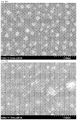
- FIG. 4 is an SEM image according to Experimental Example 1, without coating
- FIG. 5 is an SEM image according to Experimental Example 3, with a coating of a 50 nm SiOx film
- FIG. 6 is an SEM image according to Experimental Example 5, with a coating of a 100 nm SiOx film
- FIG. 7 is an SEM image according to Experimental Example 7, with a coating of a 50 nm DLC film
- FIG. 8 is an SEM image according to Experimental Example 9, with a coating of a 100 nm DLC film
- FIG. 9 is an SEM image according to Experimental Example 15, with a coating of a 100 nm DLC/50 nm SiOx/100 nm DLC laminated film;
- FIG. 10 is an SEM image according to Experimental Example 19, with a coating of a 100 nm DLC/100 nm SiOx/100 nm DLC laminated film.
- FIG. 11 is an SEM image according to Experimental Example 33, with a coating of a 50 nm SiOx/100 nm DLC laminated film.
- the thin-film laminated film according to this mode of embodiment has a structure in which one layer each or a total of three or more alternating layers of a silicon oxide-based thin film comprising silicon oxide as the main component and an amorphous carbon-based thin film are laminated on at least one surface of a plastic film constituting a base material, said thin-film laminated film comprising at least one lamination unit formed by one set in which the amorphous carbon-based thin film is formed on the silicon oxide-based thin film, and the silicon oxide-based thin film has pinholes with a diameter in the range of 10-200 nm.
- the thin-film laminated film according to this mode of embodiment includes a mode in which the amorphous carbon-based thin film formed on the silicon oxide-based thin film fits into the pinholes in the silicon oxide-based thin film.
- the amorphous carbon-based thin film formed by means of atmospheric-pressure CVD does not have a large effect in terms of improving the gas barrier properties because said film is polymer-like, but said film is flexible and improves adhesion with the base material, and therefore has strong resistance to bending.
- the silicon oxide-based thin film is formed with a large number of pinholes having a diameter of 0.01-0.2 micrometer.
- the silicon oxide-based thin film is closer to an inorganic film than the amorphous carbon-based thin film and has higher gas barrier properties excluding the pinholes.
- the silicon oxide-based thin film is dense and therefore has poor adhesion and weak resistance to bending processing.
- the deposition takes place in such a way that the amorphous carbon fills the pinholes in the silicon oxide-based thin film, and there is a dramatic improvement in the gas barrier properties while processing damage is reduced because the amorphous carbon-based thin film is buffered.
- the plastic film constituting the base material is preferably a polyester film or a nylon film.
- Polyester films include: polyethylene terephthalate (PET) resin, polyethylene terephthalate copolyester resin (e.g., a copolymer employing cyclohexanedimethanol instead of ethylene glycol in the polyester alcohol component), polybutylene terephthalate resin, and polyethylene naphthalate resin.
- PET polyethylene terephthalate
- polyethylene terephthalate copolyester resin e.g., a copolymer employing cyclohexanedimethanol instead of ethylene glycol in the polyester alcohol component
- polybutylene terephthalate resin e.g., a copolymer employing cyclohexanedimethanol instead of ethylene glycol in the polyester alcohol component
- polybutylene terephthalate resin e.g., polyethylene naphthalate resin
- Nylon films include aliphatic poly
- the film thickness is 12-50 micrometer, for example, and more preferably 12-20 micrometer.
- the film formation surface of the laminated film is one or both surfaces of the plastic film. When a film is formed on only one surface of the laminated film, it is possible to laminate a different plastic film or paper or cardboard on the surface on which a thin-film is not laminated.
- the silicon oxide-based thin film comprising silicon oxide as the main component is not limited to an SiO 2 film, and also includes an SiOx film which is a film denoted as SiO:CH or the like, in which C and H derived from an organic silicon compound are bonded to the skeleton.
- the silicon oxide-based thin film is not formed with pinholes when a vacuum method of film formation under a lower pressure than atmospheric pressure is used for the plasma CVD method (see FIG. 8 of Non-Patent Document 1, for example).
- an atmospheric-pressure method is used to form the film under atmospheric pressure, the abovementioned pinholes are formed.
- the thin-film laminated film according to this mode of embodiment therefore solves the problem of pinholes which are produced when an atmospheric-pressure method is used.
- the thickness of the silicon oxide-based thin film is preferably 5-100 nm per layer at a location where there are no pinholes, and more preferably 10-50 nm. If the film thickness is less than 5 nm, it may not be possible to achieve gas barrier properties. Furthermore, if the film thickness exceeds 100 nm, cracks are likely to form.
- the amorphous carbon-based thin film includes an amorphous hydrocarbon film (a-C:H) comprising a maximum of 50 at. % hydrogen atoms, which is DLC formed by an atmospheric-pressure method.
- the laminated thickness of the amorphous carbon-based thin film is preferably 10-150 nm per layer in a location where there are no pinholes in the silicon oxide-based thin film, and more preferably 50-100 nm. If the film thickness is less than 10 nm, it may not be possible to achieve gas barrier properties. Furthermore, if the film thickness exceeds 150 nm, cracks are likely to form. Furthermore, when lamination takes place, the thickness of the amorphous carbon-based thin film is preferably greater than the thickness of the silicon oxide-based thin film. This makes it possible to exhibit a greater effect of limiting the formation of cracks in the silicon oxide-based thin film.
- the thin-film laminated film comprises at least one lamination set in which the amorphous carbon-based thin film is formed on the silicon oxide-based thin film.
- the silicon oxide-based thin film is formed on the plastic film, and the amorphous carbon-based thin film is formed thereon.
- the silicon oxide-based thin film is formed on the plastic film, the amorphous carbon-based thin film is formed thereon, and the silicon oxide-based thin film is formed on top of that, and when further layers are laminated, those thin films are laminated alternately. Furthermore, according to a different form, the amorphous carbon-based thin film is formed on the plastic film, the silicon oxide-based thin film is formed thereon, and the amorphous carbon-based thin film is formed on top of that, and when further layers are laminated, those thin films are laminated alternately. In either form, at least one lamination unit is included.
- the thin-film laminated film according to this mode of embodiment is formed on the surface of the plastic film, and a total of three or more layers of thin films are alternately laminated, with the silicon oxide-based thin film and the amorphous carbon-based thin film being formed in succession on the amorphous carbon-based thin film.
- the amorphous carbon-based thin film By forming the amorphous carbon-based thin film on the surface of the plastic film, it is possible to achieve excellent adhesion.
- by laminating one or more sets of lamination units in which the pinholes in the silicon oxide-based thin film are covered by the amorphous carbon-based thin film it is possible to achieve high gas barrier properties.
- the upper limit for the number of layers laminated is preferably a total of 10 layers comprising layers of the silicon oxide-based thin film and layers of the amorphous carbon-based thin film. If there are more than 10 layers, the film thickness increases and there is a risk of cracks forming in the laminated thin films, while the lamination process also becomes complex, more time is needed and there are economic drawbacks in terms of practical application.
- the number of layers laminated is preferably between three and five layers.
- the method for producing the thin-film laminated film will be described next.
- the form of lamination of the thin-film laminated film is as described above.
- the following steps are each performed in order to form the amorphous carbon-based thin film or the silicon oxide-based thin film.
- the starting material gas which is used is a carbon-based starting material gas which is a mixture of a diluent gas comprising an inert gas and a hydrocarbon gas.
- An atmospheric-pressure plasma method is used, and therefore the inert gas is preferably nitrogen.
- the hydrocarbon gas is a mixture containing carbon, hydrogen and/or oxygen, and any one of acetylene, methane, ethane or propane, or a mixture thereof, is preferred.
- the concentration of hydrocarbon gas in the carbon-based starting material gas is preferably 1-10 vol % and more preferably 2-5 vol %.
- a high-frequency pulse voltage is applied under atmospheric pressure whereby the carbon-based starting material gas forms a discharge plasma, and the carbon-based starting material gas formed into a discharge plasma is brought into contact with a surface on which a film is to be formed, and the amorphous carbon-based thin film is formed on said surface.
- the pulse repeat frequency of the high-frequency pulse voltage is preferably 10-50 kHz, and more preferably 15-30 kHz.
- the applied high-frequency pulse voltage is preferably 5-30 kV at a 0-peak, and more preferably 7-20 kV.
- the pulse peak width is preferably 1-10 microseconds and more preferably 2-5 microseconds.
- the film formation time is preferably the time for the required film thickness to be achieved, but is preferably 0.5-2 seconds, for example.
- the starting material gas which is used is a metal-oxide starting material gas which is a mixture of a diluent gas comprising an inert gas, a vaporized silicon-containing organic metal compound and oxygen gas.
- the inert gas is preferably nitrogen.
- the organic metal compound is preferably at least one selected from the group consisting of: trimethylsilane (TrMS), tetraethoxysilane (TEOS), tetramethoxysilane (TMOS) and hexamethyldisiloxane (HMDSO).
- the concentration of the organic metal compound in the metal-oxide starting material gas is preferably 10-200 ppm (volume ratio), and more preferably 20-100 ppm.
- the oxygen gas concentration in the metal-oxide starting material gas is preferably 1-10 vol %, and more preferably 2-5 vol %.
- the order of mixing the inert gas, organic metal compound and oxygen gas may involve mixing the three simultaneously or mixing any two to start with and then further mixing the remaining one.
- the preferred order in this mode of embodiment involves mixing the inert gas and the organic metal compound first of all because the organic metal compound is bubbled, and then mixing the oxygen gas therewith.
- TrMS is a gas at normal temperature and atmospheric pressure, and therefore the starting material gas may be obtained by mixing the inert gas and the oxygen gas in a predetermined ratio of each.
- a high-frequency pulse voltage is applied under atmospheric pressure whereby the metal-oxide starting material gas forms a discharge plasma, and the metal-oxide starting material gas formed into a discharge plasma is brought into contact with a surface on which a film is to be formed, and the silicon oxide-based thin film is formed on said surface.
- the conditions for application of the high-frequency pulse voltage are the same as the conditions when the amorphous carbon-based thin film is formed.
- Either of the step for forming the amorphous carbon-based thin film or the step for forming the silicon oxide-based thin film may be performed first and the other may be performed next, whereby the thin films can be laminated. If required, these steps are repeated alternately. When these steps are repeated, the preceding thin-film formation step is carried out, after which the following thin-film formation step is preferably carried out within a time in the range of 0-60 seconds. The shorter the interval in lamination, the less adsorption of moisture etc. in the atmosphere and the better the adhesion between the thin films.
- the apparatus for producing the thin-film laminated film according to this mode of embodiment employs film formation in which at least two thin films are laminated by means of atmospheric-pressure plasma CVD on at least one surface of a strip-shaped plastic film constituting a base material.
- the production apparatus performs continuous film formation while the strip-shaped plastic film is conveyed, and can laminate the thin films, and has high producibility.
- the apparatus for producing the thin-film laminated film according to this mode of embodiment will be described with reference to FIG. 1 .
- FIG. 1 shows an apparatus 100 for producing the thin-film laminated film according to this mode of embodiment, where (A) is an overall view and (B) is an enlargement of a roll electrode 51 .
- the production apparatus 100 comprises at least two chambers 7 ( 7 A, 7 B) arranged in a line, and high-frequency pulse power supplies 45 , 46 .
- the chamber 7 A and the chamber 7 B are disposed in series. These chambers are also arranged in series if the production apparatus 100 comprises three or more chambers 7 (not depicted).
- the production apparatus 100 comprises a film-formation roll 1 on which the strip-shaped plastic film constituting the base material is wound, and a roll 2 for winding the strip-shaped plastic film after film formation.
- the strip-shaped plastic film wound out from the roll 1 first of all passes through the inside of the chamber 7 A in which the thin film of a first layer is formed, and then passes through the inside of the chamber 7 B in which the thin film of a second layer is formed. After exiting the chamber 7 B, the strip-shaped plastic film is turned back by means of conveyance rolls 5 , 6 for turning-back and once again passes through the inside of the chamber 7 B in which the thin film of a third layer is formed. The strip-shaped plastic film then once again passes through the inside of the chamber 7 A in which the thin film of a fourth layer is formed. The strip-shaped plastic film then exits the chamber 7 A, after which it is wound onto the roll 2 .
- the strip-shaped plastic film is a plastic film 3 on its outward path, after which it becomes a plastic film 4 on its return path.
- the conveyance route of the plastic film 3 on its outward path is determined by conveyance rolls 21 , 22 , 23 , 24 , 25 , 26 .
- the conveyance route of the plastic film 4 is determined by conveyance rolls 27 , 28 , 29 , 30 , 31 , 32 .
- the conveyance rolls 5 , 6 for turning-back pinch the plastic film therebetween. Furthermore, all of the conveyance rolls are preferably driven in synchronous rotation in such a way that the plastic film can be smoothly conveyed.
- the production apparatus 100 is such that the thin film of the first layer and the thin film of the fourth layer have the same composition (referred to as the “composition A”) and the thin film of the second layer and the thin film of the third layer have the same composition (referred to as the “composition B”).
- the resulting thin-film laminated film therefore has a three-layer structure comprising, from the bottom, the composition A/composition B/composition A on the strip-shaped plastic film.
- the chamber 7 A comprises an inlet/outlet 12 a , 12 b in a partition 8 and an inlet/outlet 13 a , 13 b in a partition 9 in order for the strip-shaped plastic films 3 , 4 to pass back and forth through the inside of the chamber 7 A.
- the distance between the film and the ends of the inlets/outlets is preferably 0.1-0.5 mm from the point of view of the inlets/outlets not interfering with the strip-shaped plastic films 3 , 4 and of minimizing the ingress and egress of gas into and out of the chamber.
- a first roll electrode group 55 comprising a plurality of roll electrodes 53 , 54 that contact a film non-formation surface of the strip-shaped plastic film 3 on its outward path and convey the strip-shaped plastic film 3 by rotating about the axis thereof
- a second roll electrode group 52 comprising a plurality of roll electrodes 50 , 51 that contact a film non-formation surface of the strip-shaped plastic film 4 on its return path and convey the strip-shaped plastic film 4 by rotating about the axis thereof, are disposed inside an internal space of the chamber 7 A, at positions such that the film-formation surface of the strip-shaped plastic film 3 on its outward path and the film-formation surface of the strip-shaped plastic film 4 on its return path are parallel with a gap therebetween.
- the interval formed by the gap (the distance between the film-formation surface of the strip-shaped plastic film 3 on its outward path and the film-formation surface of the strip-shaped plastic film 4 on its return path) is preferably 1-5 mm, and especially preferably 1-3 mm. It should be noted that the interval formed by the gap may be adjusted by the mechanism for moving the roll electrodes.
- the plurality of roll electrodes 53 , 54 in the first roll electrode group 55 are provided at an interval in such a way as not to come into contact with each other.
- FIG. 1 shows a mode in which there are two of the plurality of roll electrodes in the first roll electrode group 55 , but there may be three or more.
- the plurality of roll electrodes 50 , 51 in the second roll electrode group 52 are provided at an interval in such a way as not to come into contact with each other.
- FIG. 1 shows a mode in which there are two of the plurality of roll electrodes in the second roll electrode group 52 , but there may be three or more.
- the plurality of roll electrodes 53 , 54 in the first roll electrode group 55 and the plurality of roll electrodes 50 , 51 in the second roll electrode group 52 comprise a dielectric layer on a roll outer circumference thereof.
- the roll electrode 51 will be described with reference to FIG. 1(B) .
- the roll electrode 51 comprises a cylindrical electrode body 51 a and a rotary shaft 51 b positioned on the axis of the cylinder, and further comprises a dielectric layer 51 c on the roll outer circumference of the cylindrical electrode body 51 a .
- the other roll electrodes 50 , 53 , 54 , 56 , 57 , 59 , 60 are also the same.
- the dielectric layer 51 c has a form in which a polyimide tape, fluorine-based rubber tape, or silicone rubber tape is wound on the roll outer circumference, or a form in which an insulating oxide film such as alumina is coated on the roll outer circumference, for example.
- the whole surface of the roll outer circumference is preferably covered by the dielectric layer.
- the first roll electrode group 55 is earthed.
- the second roll electrode group 52 has a high-frequency pulse voltage applied thereto from the high-frequency pulse power supply 45 .
- the high-frequency pulse voltage may be applied to the first roll electrode group 55
- the second roll electrode group 52 may be earthed.
- the plurality of roll electrodes 53 , 54 in the first roll electrode group 55 are electrically connected to each other by a conductive member which is preferably earthed.
- the plurality of roll electrodes 50 , 51 in the second roll electrode group 52 are electrically connected to each other by a conductive member to which the high-frequency pulse voltage is preferably applied.
- the conductive member preferably conducts with the rotary shaft of the roll electrodes, for example.
- a space 71 between the first roll electrode group 55 and the second roll electrode group 52 forms a discharge space as a result of the application of the high-frequency pulse voltage.
- a starting material gas nozzle 41 for blowing out the starting material gas for forming the first layer of the thin film is further disposed in the space inside the chamber 7 A.
- the starting material gas nozzle 41 is preferably disposed at a position in front of where the plastic film 3 on its outward path and the plastic film 4 on its return path initially pass through the space 71 , as seen from the plastic film 3 on its outward path.
- the length of the space 71 in the film conveyance direction is 20-200 mm, for example.
- the starting material gas nozzle 41 blows out the starting material gas towards the discharge space (space 71 ).
- an exhaust port 42 is provided in the internal space of the chamber 7 A at a position opposite the starting material gas nozzle 41 with the space 71 therebetween. The starting material gas that has passed through the discharge space (space 71 ) is expelled through the exhaust port 42 .
- the chamber 7 B comprises an inlet/outlet 14 a , 14 b in a partition 10 and an inlet/outlet 16 a , 16 b in a partition 11 in order for the strip-shaped plastic films 3 , 4 to pass back and forth through the inside of the chamber 7 B.
- the distance between the film and the ends of the inlets/outlets is preferably 0.1-0.5 mm from the point of view of the inlets/outlets not interfering with the strip-shaped plastic films 3 , 4 and of minimizing the ingress and egress of gas into and out of the chamber.
- a first roll electrode group 61 comprising a plurality of roll electrodes 59 , 60 that contact a film non-formation surface of the strip-shaped plastic film 3 on its outward path and convey the strip-shaped plastic film 3 by rotating about the axis thereof
- a second roll electrode group 58 comprising a plurality of roll electrodes 56 , 57 that contact a film non-formation surface of the strip-shaped plastic film 4 on its return path and convey the strip-shaped plastic film 4 by rotating about the axis thereof, are disposed inside an internal space of the chamber 7 B, at positions such that the film-formation surface of the strip-shaped plastic film 3 on its outward path and the film-formation surface of the strip-shaped plastic film 4 on its return path are parallel with a gap therebetween.
- the interval formed by the gap (the distance between the film-formation surface of the strip-shaped plastic film 3 on its outward path and the film-formation surface of the strip-shaped plastic film 4 on its return path) is preferably 1-5 mm, and especially preferably 1-3 mm. It should be noted that the interval formed by the gap may be adjusted by the mechanism for moving the roll electrodes.
- the plurality of roll electrodes 59 , 60 in the first roll electrode group 61 are provided at an interval in such a way as not to come into contact with each other.
- FIG. 1 shows a mode in which there are two of the plurality of roll electrodes in the first roll electrode group 61 , but there may be three or more.
- the plurality of roll electrodes 56 , 57 in the second roll electrode group 58 are provided at an interval in such a way as not to come into contact with each other.
- FIG. 1 shows a mode in which there are two of the plurality of roll electrodes in the second roll electrode group 58 , but there may be three or more.
- the plurality of roll electrodes 59 , 60 in the first roll electrode group 61 and the plurality of roll electrodes 56 , 57 in the second roll electrode group 58 comprise a dielectric layer on a roll outer circumference thereof (this is the same as the dielectric layer 51 c of the roll electrode 51 ).
- the dielectric layer has a form in which a polyimide tape, fluorine-based rubber tape, or silicone rubber tape is wound on the roll outer circumference, or a form in which an insulating oxide film such as alumina is coated on the roll outer circumference, for example.
- the whole surface of the roll outer circumference is preferably covered by the dielectric layer.
- the first roll electrode group 61 is earthed.
- the second roll electrode group 58 has a high-frequency pulse voltage applied thereto from the high-frequency pulse power supply 46 . It should be noted that the high-frequency pulse voltage may be applied to the first roll electrode group 61 , and the second roll electrode group 58 may be earthed.
- the plurality of roll electrodes 59 , 60 in the first roll electrode group 61 are electrically connected to each other by a conductive member which is preferably earthed. Furthermore, the plurality of roll electrodes 56 , 57 in the second roll electrode group 58 are electrically connected to each other by a conductive member to which the high-frequency pulse voltage is preferably applied.
- the conductive member preferably conducts with the rotary shaft of the roll electrodes, for example.
- a space 72 between the first roll electrode group 61 and the second roll electrode group 58 forms a discharge space as a result of the application of the high-frequency pulse voltage.
- a starting material gas nozzle 43 for blowing out the starting material gas for forming the first layer of the thin film is further disposed in the space inside the chamber 7 B.
- the starting material gas nozzle 43 is preferably disposed at a position in front of where the plastic film 3 on its outward path and the plastic film 4 on its return path initially pass through the space 72 , as seen from the plastic film 3 on its outward path.
- the length of the space 72 in the film conveyance direction is 20-200 mm, for example.
- the starting material gas nozzle 43 blows out the starting material gas towards the discharge space (space 72 ).
- an exhaust port 44 is provided in the internal space of the chamber 7 B at a position opposite the starting material gas nozzle 43 with the space 72 therebetween. The starting material gas that has passed through the discharge space (space 72 ) is expelled through the exhaust port 44 .
- a central compartment 17 bounded by the partitions 9 , 10 is preferably provided between the chamber 7 A and the chamber 7 B.
- An exhaust port 15 is provided in the central compartment 17 . Gas comprising the starting material gases from the chambers 7 A, 7 B that has leaked to the central compartment 17 from the inlets/outlets 13 a , 13 b , 14 a , 14 b is expelled from the exhaust port 15 . This makes it possible to restrict mixing of the gases in the internal spaces of each of the chambers 7 A, 7 B.
- the starting material gas nozzles 41 , 43 in the adjacent chambers ( 7 A and 7 B) provide a flow of different types of starting material gases.
- the carbon-based starting material gas flows from the starting material gas nozzle 41 in the chamber 7 A, while the carbon-based starting material gas flows from the starting material gas nozzle 43 in the chamber 7 B and the metal-oxide starting material gas also flows therefrom.
- the thin-film laminated film has a three-layer structure comprising, from the bottom, the amorphous carbon-based thin film/silicon oxide-based thin film/amorphous carbon-based thin film on the strip-shaped plastic film.
- the thin-film laminated film has a three-layer structure comprising, from the bottom, the silicon oxide-based thin film/amorphous carbon-based thin film/amorphous carbon-based thin film on the strip-shaped plastic film.
- One chamber may be added at the location where the chamber 7 A, 7 B and the conveyance rolls 5 , 6 for turning-back are arranged in succession, so that the arrangement is in the following order: chamber 7 A, chamber 7 B, chamber (not depicted; referred to hereinafter as the “chamber C”), conveyance rolls 5 , 6 for turning-back.
- chamber C chamber (not depicted; referred to hereinafter as the “chamber C”)
- conveyance rolls 5 , 6 for turning-back By arranging the three chambers in series and providing flows of different types of starting material gases from the starting material gas nozzles and the adjacent chambers, it is possible to increase the number of thin films laminated.
- the thin-film laminated film has a five-layer structure comprising, from the bottom, composition A thin film/composition B thin film/composition A thin film/composition B thin film/composition A thin film on the strip-shaped plastic film.
- one or more chambers may be added between the chamber C and the conveyance rolls 5 , 6 for turning-back. This makes it possible to further increase the number of laminations.
- a production apparatus 200 will be described next with reference to FIG. 2 .
- the production apparatus 200 is provided with a pair of plate-shaped electrodes 152 , 155 .
- a high-frequency pulse power supply 145 is connected to a plate 152 a of the plate-shaped electrode 152 .
- a plate 155 a of the plate-shaped electrode 155 is earthed. This connection relationship may be reversed.
- a conveyance roll 153 for smoothly introducing the plastic films 3 , 4 into the space formed between the pair of plate-shaped electrodes 152 , 155 is preferably disposed to the front and the rear of the plate-shaped electrodes 152 , 155 in the direction of advance of the plastic films 3 , 4 .
- Dielectric layers 152 b , 155 b may be provided on the facing surfaces of the plates 152 a , 155 a , respectively.
- the dielectric layers 152 b , 155 b may be the same dielectric layers as in the production apparatus 100 .
- the surfaces of the dielectric layers 152 b , 155 b preferably have a low coefficient of friction with the plastic films 3 , 4 so that said plastic films 3 , 4 make smooth contact therewith.
- a pair of plate-shaped electrodes 158 , 161 are provided instead of the roll electrode group in the chamber 7 B.
- the pair of plate-shaped electrodes 158 , 161 preferably have the same configuration as the pair of plate-shaped electrodes 152 , 155 .
- a production apparatus 300 will be described next with reference to FIG. 3 .
- the production apparatus 300 is provided with a belt-shaped electrode group 252 in which a conductive belt 270 is wound onto belt drive rollers 250 , 251 .
- Said production apparatus is further provided with a belt-shaped electrode group 255 in which a conductive belt 271 is wound onto belt drive rollers 253 , 254 .
- the belt-shaped electrode group 252 and the belt-shaped electrode group 255 form a pair, and the belt-shaped electrode group 252 and the belt-shaped electrode group 255 are arranged in such a way that the facing surfaces of the belts 270 and 271 are parallel.
- the belt drive roller 251 can be rotated by means of a rotary shaft 251 a , and the other belt drive roller also likewise has a rotary shaft.
- the belt drive rollers 250 , 251 , 253 , 254 preferably have a mechanism for turning the belts 270 and 271 synchronously with conveyance of the plastic films 3 , 4 .
- the material of the belts 270 , 271 is preferably a metal such as gold, silver, platinum, stainless steel, copper or iron, and the facing surfaces of the belts 270 , 271 are preferably covered by dielectric layers 270 a , 271 a .
- the dielectric layers 270 a , 271 a are preferably dielectric sheets such as silicone rubber or heat-resistant plastic.
- the surface of the belt 270 opposite the surface on which the dielectric layer 270 a is provided i.e. the inside surface of the belt 270
- a high-frequency pulse power supply 245 is connected to a rotary shaft of the roll-type contact 274 .
- the surface of the belt 271 opposite the surface on which the dielectric layer 271 a is provided i.e. the inside surface of the belt 271
- a rotary shaft of the roll-type contact 275 is earthed. It should be noted that the power input and earthing connection relationship may be reversed.
- a pair of belt-shaped electrode groups 258 , 261 are provided instead of the roll electrode groups in the chamber 7 B.
- the pair of belt-shaped electrode groups 258 , 261 preferably have the same configuration as the pair of belt-shaped electrode groups 252 , 255 .
- the rate at which the thin films are formed in the chambers is adjusted through the starting material gas supply amount, starting material gas concentration and starting material gas plasma-formation conditions etc., in such a way that the required film thickness is achieved at a predetermined film conveyance rate. Furthermore, during an experimental operation to determine the film-formation conditions, said operation is carried out under conditions such that the rate at which the thin films are formed in the chambers is constant (e.g., the DLC film-formation rate is 50 nm/second and the SiOx film-formation rate is 10 nm/second), and a film may be formed in such a way as to reach the required film thickness by adjusting the film conveyance rate. In this case, the film conveyance rate can be adjusted by turning film formation in the chambers on/off at suitable times rather than film formation being permanently on.
- the chamber 7 A is on the side of the film-formation roll 1
- the chamber C is on the side of the conveyance rolls 5 , 6 .
- a nylon film (produced by Kohjin Co., Ltd.; Bonyl RX, thickness 15 micrometer) was used as the base material and was formed into a roll shape having a width of 100 mm and a length of 10 m. Furthermore, a polyethylene terephthalate film (produced by Toray Industries, Inc.; Lumirror S10, thickness 23 micrometer) was used and was formed into a roll shape having a width of 100 mm and a length of 10 m.
- the experimental conditions of the experimental examples are shown in table 1a, table 1b table 1c and table 1d. It should be noted that the gap formed by the discharge spaces (spaces 71 , 72 ) was 2 mm in all the chambers.
- the discharge plasma was formed under conditions of normal pressure at 95 kPa (0.095 MPa), and the pressures inside the chambers (including the pressure in the discharge spaces (spaces 71 , 72 )) were also kept the same.
- the high-frequency voltage was applied under conditions of a negative peak voltage of 18 kV and with a peak width at 20 kHz of 10 microseconds. Furthermore, the normal-pressure conditions were set inside the chambers by substitution with nitrogen gas at a pressure of 95 kPa.
- the roll electrodes were made of copper and the dielectric layer wound on the roll outer circumference was a silicone rubber tape. The interval in the space where plasma was generated by the facing roll electrodes was 20 mm in the direction of advance of the film.
- the metal-oxide starting material gas in the chamber B was prepared as follows.
- a starting material gas obtained by mixing a diluent gas comprising nitrogen gas, TrMS and oxygen gas was introduced to the starting material gas nozzle 43 .
- a starting material gas obtained by mixing a diluent gas comprising nitrogen gas and HMDSO in a vapour generator (evaporator) to form a precursor mixture in the form of a vapour which was then mixed with oxygen gas, was introduced to the starting material gas nozzle 43 .
- the starting material gas nozzle comprised a slit-shaped gas introduction portion and the width was the same as that of the discharge spaces (spaces 71 , 72 ).
- the exhaust port comprised a slit-shaped suction port and the width was the same as that of the discharge spaces (spaces 71 , 72 ).
- the film conveyance rate was adjusted each time in order to achieve a predetermined film thickness for each laminated layer.
- the film-formation rate of the amorphous carbon-based thin film (denoted as a DLC thin film) under the conditions of these experiments was 50 nm/second, and the film-formation rate of the silicon oxide-based thin film (denoted as an SiOx thin film) was 10 nm/second, and therefore the time of movement over the distance of 20 mm in the plasma generation space was adjusted according to the conveyance time in order to control the thickness of each layer.
- it is possible to control the thickness of each layer by changing the distance of the plasma generation space when the conveyance speed is constant in the actual apparatus used.
- Films were formed as follows in Experimental Examples 33 and 34. That is to say, a film was not formed in the chamber 7 A, rather a film was formed by passage through the chamber 7 B and a film was further formed by passage through the chamber 7 C, after which the return path involved winding without a film being formed in either the chamber 7 B or the chamber 7 A.
- the oxygen transmission coefficient (oxygen transmission rate: OTR) was measured using an oxygen transmission rate measurement apparatus (produced by Mocon, Inc.; model OX-TRAN 2/20).
- the film thickness was measured using a stylus surface profilometer (Dektak 3030, produced by Veeco Instruments, Inc., USA).
- FIG. 4 is an SEM image according to Experimental Example 1 where the base material was uncoated.
- FIG. 5 is an SEM image according to Experimental Example 3, with a coating of a 50 nm SiOx film.
- FIG. 6 is an SEM image according to Experimental Example 5, with a coating of a 100 nm SiOx film.
- FIG. 7 is an SEM image according to Experimental Example 7, with a coating of a 50 nm DLC film.
- FIG. 8 is an SEM image according to Experimental Example 9, with a coating of a 100 nm DLC film.
- FIG. 4 is an SEM image according to Experimental Example 1 where the base material was uncoated.
- FIG. 5 is an SEM image according to Experimental Example 3, with a coating of a 50 nm SiOx film.
- FIG. 6 is an SEM image according to Experimental Example 5, with a coating of a 100 nm SiOx film.
- FIG. 7 is an SEM image according to Experimental Example 7, with a coating of a 50
- FIG. 9 is an SEM image according to Experimental Example 15, with a coating of a 100 nm DLC/50 nm SiOx/100 nm DLC laminated film.
- FIG. 10 is an SEM image according to Experimental Example 19, with a coating of a 100 nm DLC/100 nm SiOx/100 nm DLC laminated film.
- FIG. 11 is an SEM image according to Experimental Example 33, with a coating of a 50 nm SiOx/100 nm DLC laminated film.
- FIG. 5 and FIG. 6 a large number of pinholes having a diameter of 10-200 nm were produced in the SiOx film formed on the base material.
- FIG. 7 and FIG. 8 pinhole formation was not apparent in the DLC film formed on the base material, and the surface was smooth.
- FIG. 9 and FIG. 10 white dot-like bodies were observed in the thin film having a three-layer structure comprising DLC/SiOx/DLC formed on the base material.
- FIG. 11 the same white dot-like bodies as in the three-layer structure were observed in the thin film having a two-layer structure comprising SiOx/DLC formed on the base material.
- the white dot-like regions in FIG. 9 and FIG. 10 could be confirmed as being traces from the pinholes formed in the SiOx thin film formed on the DLC thin film being filled by the DLC thin film formed on top.
- the DLC thin film was also formed in the regions of the SiOx thin film where there were no pinholes. It could also be confirmed that the DLC thin film formed on the SiOx thin film fitted into the pinholes in the SiOx thin film. It could be confirmed from FIG. 11 that the pinholes in the SiOx thin film were filled even when only the DLC thin film was formed on the SiOx thin film.
- the rate of improvement of the oxygen transmission rate was compared for the gas barrier properties.
- OTR oxygen transmission rate
- a polyamide film having a thickness of 15 micrometer 39 cc/day/m 2 /atm, 50% RH, 135 cc/day/m 2 /atm, 90% RH
- the OTR was 15.5 cc/day/m 2 /atm, 50% RH, 66 cc/day/m 2 /atm, 90% RH in the case of an SiOx coating formed by means of atmospheric-pressure CVD having a film thickness of 50 nm (Experimental Examples 3 and 4).
- a DLC layer formed by means of atmospheric-pressure CVD does not have a large effect in terms of improving the gas barrier properties because said film is polymer-like, but said film is flexible and improves adhesion with the base material, and therefore has strong resistance to bending; meanwhile, according to SEM observation, the SiOx film is formed with a large number of pinholes of 10-200 nm, but said film is closer to an inorganic film than the DLC thin film and has higher gas barrier properties excluding the pinholes (from a comparison of Experimental Examples 3 and 7). However, the SiOx film is dense and therefore has poor adhesion and weak resistance to bending processing.
- the DLC film When the DLC film is coated on the SiOx film, it is believed that the deposition takes place in such a way that the DLC fills the pinholes in the SiOx film, and there is a dramatic improvement in the gas barrier properties while processing damage is reduced because the DLC film is buffered. Furthermore, the DLC film is coated on the base material first of all, and therefore said DLC film provides a buffer to deformation produced in the base material as a result of moisture absorption and stress, and since it also has good adhesion with the SiOx film, this is believed to be effective for preventing the phenomenon of cracking when the SiOx film is subjected to deformation.
Landscapes
- Chemical & Material Sciences (AREA)
- Engineering & Computer Science (AREA)
- Metallurgy (AREA)
- Chemical Kinetics & Catalysis (AREA)
- Materials Engineering (AREA)
- Mechanical Engineering (AREA)
- General Chemical & Material Sciences (AREA)
- Organic Chemistry (AREA)
- Inorganic Chemistry (AREA)
- Physics & Mathematics (AREA)
- Plasma & Fusion (AREA)
- Chemical Vapour Deposition (AREA)
- Laminated Bodies (AREA)
Applications Claiming Priority (4)
| Application Number | Priority Date | Filing Date | Title |
|---|---|---|---|
| JP2015-217014 | 2015-11-04 | ||
| JP2015217014A JP6427478B2 (ja) | 2015-11-04 | 2015-11-04 | 薄膜積層フィルム、その製造方法及びその製造装置 |
| JPJP2015-217014 | 2015-11-04 | ||
| PCT/JP2016/082783 WO2017078133A1 (en) | 2015-11-04 | 2016-11-04 | Laminated film |
Publications (2)
| Publication Number | Publication Date |
|---|---|
| US20180320268A1 US20180320268A1 (en) | 2018-11-08 |
| US10934624B2 true US10934624B2 (en) | 2021-03-02 |
Family
ID=57442765
Family Applications (1)
| Application Number | Title | Priority Date | Filing Date |
|---|---|---|---|
| US15/773,499 Active US10934624B2 (en) | 2015-11-04 | 2016-11-04 | Laminated film |
Country Status (6)
| Country | Link |
|---|---|
| US (1) | US10934624B2 (https=) |
| EP (1) | EP3371339B1 (https=) |
| JP (1) | JP6427478B2 (https=) |
| CN (1) | CN108368610A (https=) |
| ES (1) | ES2908465T3 (https=) |
| WO (1) | WO2017078133A1 (https=) |
Cited By (1)
| Publication number | Priority date | Publication date | Assignee | Title |
|---|---|---|---|---|
| US20230217839A1 (en) * | 2021-02-26 | 2023-07-06 | Metox Technologies, Inc. | Multi-Stack Susceptor Reactor for High-Throughput Superconductor Manufacturing |
Families Citing this family (2)
| Publication number | Priority date | Publication date | Assignee | Title |
|---|---|---|---|---|
| ES3040230T3 (en) * | 2019-02-19 | 2025-10-29 | Xefco Pty Ltd | System for treatment and/or coating of substrates |
| CN111925552B (zh) * | 2020-08-04 | 2022-11-22 | 佛山金万达科技股份有限公司 | 热塑性树脂薄膜的表面处理及所得产品 |
Citations (16)
| Publication number | Priority date | Publication date | Assignee | Title |
|---|---|---|---|---|
| JPH09272567A (ja) | 1996-02-09 | 1997-10-21 | Kirin Brewery Co Ltd | コーティングフィルムおよびその製造方法 |
| JPH11245327A (ja) | 1998-02-27 | 1999-09-14 | Sony Corp | 保護膜およびその形成方法 |
| JPH11348171A (ja) | 1998-06-08 | 1999-12-21 | Dainippon Printing Co Ltd | 透明バリア性フィルムおよびそれを使用した積層体 |
| US6027793A (en) * | 1997-11-03 | 2000-02-22 | Alusuisse Technology & Management Ltd. | Packaging film |
| JP2002151507A (ja) | 2000-11-15 | 2002-05-24 | Sekisui Chem Co Ltd | 半導体素子の製造方法及びその装置 |
| JP2003171770A (ja) | 2001-04-27 | 2003-06-20 | Konica Corp | プラズマ放電処理装置、プラズマ放電処理方法、その方法で製造された薄膜及び積層体、及び光学フィルム、光学フィルムを用いた偏光板及び表示装置 |
| US20040146667A1 (en) * | 2001-06-26 | 2004-07-29 | Kenichi Hama | Manufacturing device for dlc film coated plastic container, dlc film coated plastic container, and method of manufacturing the dlc film coated plastic container |
| US20040161534A1 (en) | 2003-02-18 | 2004-08-19 | Ngk Insulators, Ltd. | Thin films and a method for producing the same |
| JP2005088452A (ja) * | 2003-09-18 | 2005-04-07 | Dainippon Printing Co Ltd | ガスバリア性フィルム及びそれを用いてなる積層体 |
| US20070031674A1 (en) * | 2002-05-07 | 2007-02-08 | Tolt Zhidan L | Barrier, such as a hermetic barrier layer for O/PLED and other electronic devices on plastic |
| JP2008094447A (ja) | 2006-10-13 | 2008-04-24 | Toppan Printing Co Ltd | 薄膜被覆されたプラスチック容器 |
| WO2008096617A1 (ja) | 2007-02-06 | 2008-08-14 | Konica Minolta Holdings, Inc. | 透明ガスバリア性フィルム及び透明ガスバリア性フィルムの製造方法 |
| JP2009161782A (ja) | 2007-12-28 | 2009-07-23 | Konica Minolta Business Technologies Inc | 大気圧プラズマ処理装置 |
| WO2010100971A1 (ja) * | 2009-03-04 | 2010-09-10 | コニカミノルタホールディングス株式会社 | 薄膜を有する基材 |
| JP2010208277A (ja) | 2009-03-12 | 2010-09-24 | Kanagawa Acad Of Sci & Technol | プラスチック系材料およびその製造方法 |
| JP2014065281A (ja) | 2012-09-27 | 2014-04-17 | Keio Gijuku | 積層体とその製造方法 |
Family Cites Families (1)
| Publication number | Priority date | Publication date | Assignee | Title |
|---|---|---|---|---|
| JP5223466B2 (ja) * | 2008-05-30 | 2013-06-26 | 大日本印刷株式会社 | ガスバリア性フィルム及びその製造方法 |
-
2015
- 2015-11-04 JP JP2015217014A patent/JP6427478B2/ja active Active
-
2016
- 2016-11-04 US US15/773,499 patent/US10934624B2/en active Active
- 2016-11-04 WO PCT/JP2016/082783 patent/WO2017078133A1/en not_active Ceased
- 2016-11-04 EP EP16804917.9A patent/EP3371339B1/en active Active
- 2016-11-04 ES ES16804917T patent/ES2908465T3/es active Active
- 2016-11-04 CN CN201680064665.6A patent/CN108368610A/zh active Pending
Patent Citations (19)
| Publication number | Priority date | Publication date | Assignee | Title |
|---|---|---|---|---|
| JPH09272567A (ja) | 1996-02-09 | 1997-10-21 | Kirin Brewery Co Ltd | コーティングフィルムおよびその製造方法 |
| US6027793A (en) * | 1997-11-03 | 2000-02-22 | Alusuisse Technology & Management Ltd. | Packaging film |
| JPH11245327A (ja) | 1998-02-27 | 1999-09-14 | Sony Corp | 保護膜およびその形成方法 |
| JPH11348171A (ja) | 1998-06-08 | 1999-12-21 | Dainippon Printing Co Ltd | 透明バリア性フィルムおよびそれを使用した積層体 |
| JP2002151507A (ja) | 2000-11-15 | 2002-05-24 | Sekisui Chem Co Ltd | 半導体素子の製造方法及びその装置 |
| JP2003171770A (ja) | 2001-04-27 | 2003-06-20 | Konica Corp | プラズマ放電処理装置、プラズマ放電処理方法、その方法で製造された薄膜及び積層体、及び光学フィルム、光学フィルムを用いた偏光板及び表示装置 |
| US20040146667A1 (en) * | 2001-06-26 | 2004-07-29 | Kenichi Hama | Manufacturing device for dlc film coated plastic container, dlc film coated plastic container, and method of manufacturing the dlc film coated plastic container |
| US20070031674A1 (en) * | 2002-05-07 | 2007-02-08 | Tolt Zhidan L | Barrier, such as a hermetic barrier layer for O/PLED and other electronic devices on plastic |
| US20040161534A1 (en) | 2003-02-18 | 2004-08-19 | Ngk Insulators, Ltd. | Thin films and a method for producing the same |
| JP2005088452A (ja) * | 2003-09-18 | 2005-04-07 | Dainippon Printing Co Ltd | ガスバリア性フィルム及びそれを用いてなる積層体 |
| JP2008094447A (ja) | 2006-10-13 | 2008-04-24 | Toppan Printing Co Ltd | 薄膜被覆されたプラスチック容器 |
| WO2008096617A1 (ja) | 2007-02-06 | 2008-08-14 | Konica Minolta Holdings, Inc. | 透明ガスバリア性フィルム及び透明ガスバリア性フィルムの製造方法 |
| EP2123446A1 (en) | 2007-02-06 | 2009-11-25 | Konica Minolta Holdings, Inc. | Transparent gas barrier film and method for producing transparent gas barrier film |
| US20100003482A1 (en) * | 2007-02-06 | 2010-01-07 | Konica Minolta Holdings, Inc. | Transparent gas barrier film and method for producing transparent gas barrier film |
| US8846187B2 (en) | 2007-02-06 | 2014-09-30 | Konica Minolta Holdings, Inc. | Transparent gas barrier film and method for producing transparent gas barrier film |
| JP2009161782A (ja) | 2007-12-28 | 2009-07-23 | Konica Minolta Business Technologies Inc | 大気圧プラズマ処理装置 |
| WO2010100971A1 (ja) * | 2009-03-04 | 2010-09-10 | コニカミノルタホールディングス株式会社 | 薄膜を有する基材 |
| JP2010208277A (ja) | 2009-03-12 | 2010-09-24 | Kanagawa Acad Of Sci & Technol | プラスチック系材料およびその製造方法 |
| JP2014065281A (ja) | 2012-09-27 | 2014-04-17 | Keio Gijuku | 積層体とその製造方法 |
Non-Patent Citations (8)
| Title |
|---|
| Ahmet G. Erlat et al., SiOx Gas Barrier Coatings on Polymer Substrates: Morphology and Gas Transport Considerations, 103 J. Phys. Chem. B 6047 (1999) (9 pages). |
| Espacenet Translation of JP-11245327-A (Year: 2019). * |
| Espacenet Translation of JP-2005088452-A (Year: 2019). * |
| EspacenetTranslation of WO-2010100971-A1 via JP5780154 (JP Equivalent) (Year: 2019). * |
| Inagaki, Tasaka, and Hiramatu, Journal of Applied Polymer Science, vol. 71,2091-2100 (1999). |
| International Search Report from corresponding PCT Application No. PCT/JP2016/082783 dated Mar. 31, 2017 (5 pages). |
| Ladwig, A. M., Koch, R. D., Wenski, E. G., & Hicks, R. F. (2009). Atmospheric plasma deposition of diamond-like carbon coatings. Diamond and Related Materials, 18(9), 1129-1133. (Year: 2009). * |
| Office Action in corresponding Japanese Application 2015-217014 dated Aug. 7, 2018 (6 pages). |
Cited By (2)
| Publication number | Priority date | Publication date | Assignee | Title |
|---|---|---|---|---|
| US20230217839A1 (en) * | 2021-02-26 | 2023-07-06 | Metox Technologies, Inc. | Multi-Stack Susceptor Reactor for High-Throughput Superconductor Manufacturing |
| US11910726B2 (en) * | 2021-02-26 | 2024-02-20 | Metox International, Inc. | Multi-stack susceptor reactor for high-throughput superconductor manufacturing |
Also Published As
| Publication number | Publication date |
|---|---|
| EP3371339A1 (en) | 2018-09-12 |
| EP3371339B1 (en) | 2022-01-05 |
| ES2908465T3 (es) | 2022-04-29 |
| CN108368610A (zh) | 2018-08-03 |
| US20180320268A1 (en) | 2018-11-08 |
| JP2017087465A (ja) | 2017-05-25 |
| JP6427478B2 (ja) | 2018-11-21 |
| WO2017078133A1 (en) | 2017-05-11 |
Similar Documents
| Publication | Publication Date | Title |
|---|---|---|
| JP5267714B2 (ja) | 透明ガスバリア性フィルムの製造方法および有機エレクトロルミネッセンス素子 | |
| JP5136114B2 (ja) | ガスバリア膜の作製方法及び作製装置 | |
| TWI728283B (zh) | 沉積設備、塗佈軟質基材的方法、及具有塗層的軟質基材 | |
| CN101611168A (zh) | 连续成膜装置 | |
| US10934624B2 (en) | Laminated film | |
| JP2012126969A (ja) | プラズマcvd装置 | |
| WO2007026545A1 (ja) | プラズマ放電処理装置及びガスバリア性フィルムの製造方法 | |
| CN100559513C (zh) | 透明导电膜 | |
| TWI713937B (zh) | 用以塗佈撓性基板的沉積設備、塗佈撓性基板之方法及具有塗佈之撓性基板 | |
| WO2006067952A1 (ja) | ガスバリア性薄膜積層体、ガスバリア性樹脂基材、有機elデバイス | |
| US20110214609A1 (en) | Atmospheric plasma apparatus | |
| JP5719106B2 (ja) | 透明ガスバリア性フィルム及び透明ガスバリア性フィルムの製造方法 | |
| JP2006097105A (ja) | 大気圧プラズマ処理装置 | |
| JP6392494B2 (ja) | 高防湿性フィルム及びその製造方法 | |
| JP2014000782A (ja) | 積層フィルム | |
| JP6607279B2 (ja) | 高防湿性フィルム及びその製造方法 | |
| JP2006175633A (ja) | ガスバリア性薄膜積層体、及びガスバリア性樹脂基材、及び有機elデバイス | |
| EP4689224A1 (en) | Coatings with bilayer arrangements | |
| JP2026513557A (ja) | 材料加工機、多層材料を製造するための方法、及び多層材料 | |
| JP6897567B2 (ja) | ガスバリアーフィルム | |
| JP4821324B2 (ja) | 透明でガスバリア性の高い基材及びその製造方法 | |
| CN121127623A (zh) | 材料加工机、用于生产多层材料的方法以及多层材料 | |
| JP2020007618A (ja) | 積層成膜装置 | |
| JP2018108643A (ja) | フィルム積層体、その製造方法及び成膜装置 |
Legal Events
| Date | Code | Title | Description |
|---|---|---|---|
| FEPP | Fee payment procedure |
Free format text: ENTITY STATUS SET TO UNDISCOUNTED (ORIGINAL EVENT CODE: BIG.); ENTITY STATUS OF PATENT OWNER: LARGE ENTITY |
|
| AS | Assignment |
Owner name: KEIO UNIVERSITY, JAPAN Free format text: ASSIGNMENT OF ASSIGNORS INTEREST;ASSIGNORS:SUZUKI, TETSUYA;FUTAGAMI, YUYA;SHIRAKURA, AKIRA;AND OTHERS;SIGNING DATES FROM 20180418 TO 20180507;REEL/FRAME:045741/0465 Owner name: TETRA LAVAL HOLDINGS & FINANCE S.A., SWITZERLAND Free format text: ASSIGNMENT OF ASSIGNORS INTEREST;ASSIGNORS:SUZUKI, TETSUYA;FUTAGAMI, YUYA;SHIRAKURA, AKIRA;AND OTHERS;SIGNING DATES FROM 20180418 TO 20180507;REEL/FRAME:045741/0465 |
|
| STPP | Information on status: patent application and granting procedure in general |
Free format text: DOCKETED NEW CASE - READY FOR EXAMINATION |
|
| STPP | Information on status: patent application and granting procedure in general |
Free format text: NON FINAL ACTION MAILED |
|
| STPP | Information on status: patent application and granting procedure in general |
Free format text: PRE-INTERVIEW COMMUNICATION MAILED |
|
| STPP | Information on status: patent application and granting procedure in general |
Free format text: NON FINAL ACTION MAILED |
|
| STPP | Information on status: patent application and granting procedure in general |
Free format text: RESPONSE TO NON-FINAL OFFICE ACTION ENTERED AND FORWARDED TO EXAMINER |
|
| STPP | Information on status: patent application and granting procedure in general |
Free format text: FINAL REJECTION MAILED |
|
| STPP | Information on status: patent application and granting procedure in general |
Free format text: DOCKETED NEW CASE - READY FOR EXAMINATION |
|
| STPP | Information on status: patent application and granting procedure in general |
Free format text: NOTICE OF ALLOWANCE MAILED -- APPLICATION RECEIVED IN OFFICE OF PUBLICATIONS |
|
| STCF | Information on status: patent grant |
Free format text: PATENTED CASE |
|
| MAFP | Maintenance fee payment |
Free format text: PAYMENT OF MAINTENANCE FEE, 4TH YEAR, LARGE ENTITY (ORIGINAL EVENT CODE: M1551); ENTITY STATUS OF PATENT OWNER: LARGE ENTITY Year of fee payment: 4 |