US10916938B2 - ESD-protective surface-mount composite component - Google Patents
ESD-protective surface-mount composite component Download PDFInfo
- Publication number
- US10916938B2 US10916938B2 US16/229,115 US201816229115A US10916938B2 US 10916938 B2 US10916938 B2 US 10916938B2 US 201816229115 A US201816229115 A US 201816229115A US 10916938 B2 US10916938 B2 US 10916938B2
- Authority
- US
- United States
- Prior art keywords
- esd
- mount
- inductor
- thin
- conductor
- Prior art date
- Legal status (The legal status is an assumption and is not a legal conclusion. Google has not performed a legal analysis and makes no representation as to the accuracy of the status listed.)
- Active, expires
Links
- 239000002131 composite material Substances 0.000 title claims abstract description 121
- 239000004020 conductor Substances 0.000 claims abstract description 178
- 239000010409 thin film Substances 0.000 claims abstract description 86
- 239000003990 capacitor Substances 0.000 claims description 56
- 239000000758 substrate Substances 0.000 claims description 30
- 230000003071 parasitic effect Effects 0.000 claims description 12
- 239000004065 semiconductor Substances 0.000 description 30
- 239000010410 layer Substances 0.000 description 26
- 239000000463 material Substances 0.000 description 11
- 238000000034 method Methods 0.000 description 7
- 238000010586 diagram Methods 0.000 description 4
- 230000008054 signal transmission Effects 0.000 description 4
- 230000000694 effects Effects 0.000 description 3
- 239000011229 interlayer Substances 0.000 description 3
- 238000004519 manufacturing process Methods 0.000 description 3
- 230000005684 electric field Effects 0.000 description 2
- 239000000696 magnetic material Substances 0.000 description 2
- 230000005540 biological transmission Effects 0.000 description 1
- 238000003780 insertion Methods 0.000 description 1
- 230000037431 insertion Effects 0.000 description 1
- 230000007257 malfunction Effects 0.000 description 1
- 239000011347 resin Substances 0.000 description 1
- 229920005989 resin Polymers 0.000 description 1
- 238000004804 winding Methods 0.000 description 1
Images


Classifications
-
- H—ELECTRICITY
- H02—GENERATION; CONVERSION OR DISTRIBUTION OF ELECTRIC POWER
- H02H—EMERGENCY PROTECTIVE CIRCUIT ARRANGEMENTS
- H02H9/00—Emergency protective circuit arrangements for limiting excess current or voltage without disconnection
- H02H9/04—Emergency protective circuit arrangements for limiting excess current or voltage without disconnection responsive to excess voltage
- H02H9/045—Emergency protective circuit arrangements for limiting excess current or voltage without disconnection responsive to excess voltage adapted to a particular application and not provided for elsewhere
-
- H—ELECTRICITY
- H01—ELECTRIC ELEMENTS
- H01F—MAGNETS; INDUCTANCES; TRANSFORMERS; SELECTION OF MATERIALS FOR THEIR MAGNETIC PROPERTIES
- H01F17/00—Fixed inductances of the signal type
- H01F17/0006—Printed inductances
- H01F17/0013—Printed inductances with stacked layers
-
- H—ELECTRICITY
- H01—ELECTRIC ELEMENTS
- H01L—SEMICONDUCTOR DEVICES NOT COVERED BY CLASS H10
- H01L27/00—Devices consisting of a plurality of semiconductor or other solid-state components formed in or on a common substrate
- H01L27/02—Devices consisting of a plurality of semiconductor or other solid-state components formed in or on a common substrate including semiconductor components specially adapted for rectifying, oscillating, amplifying or switching and having potential barriers; including integrated passive circuit elements having potential barriers
- H01L27/0203—Particular design considerations for integrated circuits
- H01L27/0248—Particular design considerations for integrated circuits for electrical or thermal protection, e.g. electrostatic discharge [ESD] protection
-
- H—ELECTRICITY
- H01—ELECTRIC ELEMENTS
- H01L—SEMICONDUCTOR DEVICES NOT COVERED BY CLASS H10
- H01L28/00—Passive two-terminal components without a potential-jump or surface barrier for integrated circuits; Details thereof; Multistep manufacturing processes therefor
- H01L28/40—Capacitors
- H01L28/60—Electrodes
-
- H—ELECTRICITY
- H02—GENERATION; CONVERSION OR DISTRIBUTION OF ELECTRIC POWER
- H02H—EMERGENCY PROTECTIVE CIRCUIT ARRANGEMENTS
- H02H9/00—Emergency protective circuit arrangements for limiting excess current or voltage without disconnection
- H02H9/04—Emergency protective circuit arrangements for limiting excess current or voltage without disconnection responsive to excess voltage
-
- H—ELECTRICITY
- H03—ELECTRONIC CIRCUITRY
- H03H—IMPEDANCE NETWORKS, e.g. RESONANT CIRCUITS; RESONATORS
- H03H7/00—Multiple-port networks comprising only passive electrical elements as network components
- H03H7/01—Frequency selective two-port networks
- H03H7/0115—Frequency selective two-port networks comprising only inductors and capacitors
-
- H—ELECTRICITY
- H01—ELECTRIC ELEMENTS
- H01F—MAGNETS; INDUCTANCES; TRANSFORMERS; SELECTION OF MATERIALS FOR THEIR MAGNETIC PROPERTIES
- H01F17/00—Fixed inductances of the signal type
- H01F17/0006—Printed inductances
- H01F17/0013—Printed inductances with stacked layers
- H01F2017/0026—Multilayer LC-filter
-
- H—ELECTRICITY
- H01—ELECTRIC ELEMENTS
- H01F—MAGNETS; INDUCTANCES; TRANSFORMERS; SELECTION OF MATERIALS FOR THEIR MAGNETIC PROPERTIES
- H01F27/00—Details of transformers or inductances, in general
- H01F27/28—Coils; Windings; Conductive connections
- H01F27/29—Terminals; Tapping arrangements for signal inductances
- H01F27/292—Surface mounted devices
-
- H—ELECTRICITY
- H01—ELECTRIC ELEMENTS
- H01L—SEMICONDUCTOR DEVICES NOT COVERED BY CLASS H10
- H01L25/00—Assemblies consisting of a plurality of individual semiconductor or other solid state devices ; Multistep manufacturing processes thereof
- H01L25/16—Assemblies consisting of a plurality of individual semiconductor or other solid state devices ; Multistep manufacturing processes thereof the devices being of types provided for in two or more different main groups of groups H01L27/00 - H01L33/00, or in a single subclass of H10K, H10N, e.g. forming hybrid circuits
-
- H—ELECTRICITY
- H02—GENERATION; CONVERSION OR DISTRIBUTION OF ELECTRIC POWER
- H02H—EMERGENCY PROTECTIVE CIRCUIT ARRANGEMENTS
- H02H9/00—Emergency protective circuit arrangements for limiting excess current or voltage without disconnection
- H02H9/04—Emergency protective circuit arrangements for limiting excess current or voltage without disconnection responsive to excess voltage
- H02H9/045—Emergency protective circuit arrangements for limiting excess current or voltage without disconnection responsive to excess voltage adapted to a particular application and not provided for elsewhere
- H02H9/046—Emergency protective circuit arrangements for limiting excess current or voltage without disconnection responsive to excess voltage adapted to a particular application and not provided for elsewhere responsive to excess voltage appearing at terminals of integrated circuits
Definitions
- the present disclosure relates to a surface-mount composite component with an ESD protection function (or ESD-protective surface-mount composite component) including a diode and an inductor.
- ESD protection function or ESD-protective surface-mount composite component
- ESD electro-static discharge
- a radio transmitter disclosed in Patent Document 1 includes an ESD protection circuit between an antenna terminal and a transmitting circuit and a receiving circuit (hereinafter collectively referred to as a transmitting and receiving circuit).
- the ESD protection circuit has a filter function as well as the ESD protection function.
- the ESD protection circuit includes an inductor, a varistor, and capacitors.
- the inductor is connected between the transmitting and receiving circuit and the antenna terminal.
- the varistor is connected between one terminal of the inductor and the ground.
- One of the capacitors is connected between the other terminal of the inductor and the ground, and the other capacitor is connected in parallel to the inductor.
- an inductor, a varistor, and a capacitor have conventionally been separate surface-mount components.
- the inductor, the varistor, and the capacitor are individually mounted on a base circuit board (printed wiring board).
- Patent Document 1 Japanese Unexamined Patent Application Publication No. 2008-54055.
- the ESD protection circuit requires a large space, because its circuit elements are separate surface-mount components individually mounted on the base circuit board. Since the inductor, the varistor, and the capacitor are connected by a routing conductor on the base circuit board, the ESD protection circuit may not be able to achieve desired characteristics of a filter circuit.
- an object of the present invention is to provide an ESD-protective surface-mount composite component that provides desired characteristics and also achieves a compact size compared with conventional designs.
- an ESD-protective surface-mount composite component includes a surface-mount inductor and a thin-film component.
- the surface-mount inductor includes a rectangular-parallelepiped-shaped body containing a magnetic material, an inductor conductor formed inside the body, a first outer conductor and a second outer conductor connected to the inductor conductor and individually formed at both ends of the body in a first direction.
- a third outer conductor is formed at an intermediate position of the body in the first direction.
- the thin-film component includes a flat plate-like body, an ESD protection element formed inside the body, a first terminal conductor connected to a first terminal of the ESD protection element and formed on a front surface of the body, and a second terminal conductor connected to a second terminal of the ESD protection element and formed on the front surface of the body.
- the thin-film component is mounted on a first surface of the body parallel to the first direction in such a manner that the first terminal conductor is connected to the first outer conductor and the second terminal conductor is connected to the third outer conductor.
- the thin-film component is directly mounted on the inductor.
- this configuration eliminates the need for a routing conductor that connects the thin-film component and the inductor mounted on the routing conductor. Without the routing conductor, there is no impact of inductance of the routing conductor on characteristics.
- a parasitic capacitor of the ESD protection element and the inductor may form a filter.
- the thin-film component includes a capacitor formed inside the body and a third terminal conductor formed on the front surface of the body.
- a first counter electrode of the capacitor is connected to the second terminal conductor, and a second counter electrode of the capacitor is connected to the third terminal conductor.
- the third terminal conductor is mounted on the second outer conductor.
- the capacitor, a parasitic capacitor of the ESD protection element, and the inductor may form a filter.
- an area of the thin-film component is smaller than an area of the first surface, and as viewed in a direction orthogonal to the first surface, the thin-film component overlaps the first surface.
- the plane area of the ESD-protective surface-mount composite component is equal to the plane area of the surface-mount inductor.
- the ESD-protective surface-mount composite component is thus compact in size.
- an area of the thin-film component is larger than an area of the first surface, and as viewed in a direction orthogonal to the first surface, the thin-film component overlaps the first surface.
- the plane area of the ESD-protective surface-mount composite component is larger than the plane area of the surface-mount inductor.
- this improves efficiency in producing ESD-protective surface-mount composite components, because inductors can be joined to an array of thin-film components formed in a motherboard.
- the exemplary embodiments of the present invention provide a compact ESD-protective surface-mount composite component that can achieve desired characteristics.
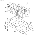
- FIG. 1 is an external perspective view of an ESD-protective surface-mount composite component according to a first exemplary embodiment.
- FIG. 2(A) is a side cross-sectional view of the ESD-protective surface-mount composite component according to the first exemplary embodiment
- FIG. 2(B) is a side view of the ESD-protective surface-mount composite component
- FIG. 2(C) is a plan view of the ESD-protective surface-mount composite component.
- FIG. 3 is an equivalent circuit diagram of the ESD-protective surface-mount composite component according to the first exemplary embodiment.
- FIG. 4(A) is a side cross-sectional view illustrating how the ESD-protective surface-mount composite component according to the first exemplary embodiment is mounted on an external circuit substrate
- FIG. 4(B) is an external perspective view illustrating mounting onto the external circuit substrate.
- FIG. 5 is an exploded perspective view schematically illustrating a configuration of an inductor according to the first exemplary embodiment.
- FIG. 6 is a cross-sectional view schematically illustrating a configuration of a thin-film component according to the first exemplary embodiment.
- FIG. 7 is a side cross-sectional view of an ESD-protective surface-mount composite component according to a second exemplary embodiment.
- FIG. 8 is an equivalent circuit diagram of the ESD-protective surface-mount composite component according to the second exemplary embodiment.
- FIG. 9(A) is a side view of an ESD-protective surface-mount composite component according to a third exemplary embodiment
- FIG. 9(B) is a plan view of the ESD-protective surface-mount composite component.
- FIG. 10 is a flowchart outlining a process of manufacturing ESD-protective surface-mount composite components 10 B according to the third exemplary embodiment.
- FIG. 11 schematically illustrates how surface-mount inductors are mounted on a motherboard.
- FIG. 12 is a side view of an ESD-protective surface-mount composite component according to a fourth exemplary embodiment.
- FIG. 13 is an external perspective view illustrating how the ESD-protective surface-mount composite component according to the fourth exemplary embodiment is mounted on the external circuit substrate.
- FIG. 1 is an external perspective view of the ESD-protective surface-mount composite component according to the first embodiment.
- FIG. 2(A) is a side cross-sectional view of the ESD-protective surface-mount composite component according to the first embodiment
- FIG. 2(B) is a side view of the ESD-protective surface-mount composite component
- FIG. 2(C) is a plan view of the ESD-protective surface-mount composite component. Note that FIG. 2(A) illustrates a cross-section taken along line A-A in FIG. 1 , but does not show the internal structure of a thin-film component 30 .
- an ESD-protective surface-mount composite component 10 includes a surface-mount inductor 20 and the thin-film component 30 coupled thereto.
- the surface-mount inductor 20 includes a body 200 , a first outer conductor 211 , a second outer conductor 212 , and a third outer conductor 213 .
- the body 200 is made of a material containing a magnetic material. Inductor conductors are formed inside the body 200 . The configuration of the body 200 will be detailed later on.
- the body 200 is in the shape of a rectangular parallelepiped. Specifically, as illustrated in FIG. 1 , the body 200 has predetermined dimensions in three axis directions (X-direction, Y-direction, and Z-direction) orthogonal to each other.
- the (dimension in X-direction) ⁇ (dimension in Y-direction) is about 1.0 (mm) ⁇ about 0.5 (mm) or about 0.6 (mm) ⁇ about 0.3 (mm).
- the dimension in the Z-axis is substantially equal to the dimension in the Y-direction.
- the X-direction corresponds to “first direction” of the present disclosure.
- the body 200 has, at one end thereof in the Z-direction, a first surface 21 parallel to the X-direction and also has, at the other end thereof in the Z-direction, a second surface 22 parallel to the X-direction.
- the body 200 has, at one end thereof in the X-direction, a first end face 23 parallel to the Z-direction and also has, at the other end thereof in the X-direction, a second end face 24 parallel to the Z-direction.
- the body 200 also has, at both ends thereof in the Y-direction, side surfaces parallel to the X-direction.
- the first outer conductor 211 is formed at a first end portion (i.e., a first end) of the body 200 in the X-direction.
- the first outer conductor 211 is shaped to cover the entire area of the first end face 23 and extend over part of each of the first surface 21 , the second surface 22 , and the side surfaces.
- the first outer conductor 211 is connected to one ends of the inductor conductors inside the body 200 .
- the second outer conductor 212 is formed at a second end portion (i.e., a second end opposite the first end) of the body 200 in the X-direction.
- the second outer conductor 212 is shaped to cover the entire area of the second end face 24 and extend over part of each of the first surface 21 , the second surface 22 , and the side surfaces.
- the second outer conductor 212 is connected to the other ends of the inductor conductors inside the body 200 .
- the second outer conductor 212 and the first outer conductor 211 are spaced apart.
- the third outer conductor 213 is formed at an intermediate position (e.g., a middle or center portion) of the body 200 in the X-direction.
- the third outer conductor 213 is shaped to extend over the first surface 21 , the second surface 22 , and the side surfaces.
- the third outer conductor 213 is spaced from both the first outer conductor 211 and the second outer conductor 212 .
- the first outer conductor 211 , the third outer conductor 213 , and the second outer conductor 212 are arranged on the body 200 along the first direction and spaced apart from one another.
- the thin-film component 30 includes a body 300 , a first terminal conductor 311 , a second terminal conductor 312 , and a third terminal conductor 313 .
- the body 300 is a flat plate-like member and includes a semiconductor diode and a capacitor C therein.
- the semiconductor diode corresponds to “ESD protection element” of the present disclosure.
- the configuration of the body 300 will be detailed later on. According to an exemplary aspect, for example, the (dimension in X-direction) ⁇ (dimension in Y-direction) of the body 300 is about 0.95 (mm) ⁇ about 0.45 (mm) when the body 200 of the inductor 20 measures 1.0 (mm) ⁇ 0.5 (mm), and the (dimension in X-direction) ⁇ (dimension in Y-direction) of the body 300 is about 0.55 (mm) ⁇ about 0.25 (mm) when the body 200 of the inductor 20 measures 0.6 (mm) ⁇ 0.3 (mm).
- the body 300 has a front surface 32 at one end thereof in the Z-direction (e.g., a side surface), and has a back surface 31 at the other end thereof in the Z-direction (e.g., another side surface).
- the first terminal conductor 311 , the second terminal conductor 312 , and the third terminal conductor 313 are formed to be exposed to the front surface 32 of the body 300 .
- the first terminal conductor 311 , the second terminal conductor 312 , and the third terminal conductor 313 are arranged to be spaced apart along the X-direction.
- the first terminal conductor 311 is formed near a first end of the body 300 in the X-direction
- the third terminal conductor 313 is formed near a second end of the body 300 in the X-direction
- the second terminal conductor 312 is formed at an intermediate position of the body 300 in the X-direction.
- the first terminal conductor 311 is connected to a first end of an ESD protection element TVS formed by a semiconductor diode
- the second terminal conductor 312 is connected to a second end of the ESD protection element TVS. That is, the first terminal conductor 311 and the second terminal conductor 312 are electrically connected through the ESD protection element TVS.
- the second terminal conductor 312 is connected to a first counter electrode of the capacitor C
- the third terminal conductor 313 is connected to a second counter electrode of the capacitor C. That is, the second terminal conductor 312 and the third terminal conductor 313 are electrically connected through the capacitor C.
- the thin-film component 30 is mounted on (i.e., coupled thereto) the first surface 21 of the inductor 20 .
- the first terminal conductor 311 of the thin-film component 30 and the first outer conductor 211 of the inductor 20 are connected, with a conductive joining material 41 interposed therebetween.
- the second terminal conductor 312 of the thin-film component 30 and the third outer conductor 213 of the inductor 20 are connected, with the conductive joining material 41 interposed therebetween.
- the third terminal conductor 313 of the thin-film component 30 and the second outer conductor 212 of the inductor 20 are connected, with the conductive joining material 41 interposed therebetween.
- FIG. 3 is an equivalent circuit diagram of the ESD-protective surface-mount composite component according to the first embodiment of the present invention.
- the ESD-protective surface-mount composite component 10 includes an inductor L, the ESD protection element TVS, and the capacitor C.
- the ESD-protective surface-mount composite component 10 also includes a first terminal P 1 , a second terminal P 2 , and a third terminal P 3 .
- the inductor L is connected between the first terminal P 1 and the second terminal P 2 .
- the ESD protection element TVS is connected between the first terminal P 1 and the third terminal P 3 .
- the capacitor C is connected between the second terminal P 2 and the third terminal P 3 .
- the ESD protection element TVS has a parasitic capacitor Ctvs, and the parasitic capacitor Ctvs is connected in parallel to the ESD protection element TVS in the equivalent circuit.
- the first terminal P 1 and the second terminal P 2 are terminals for inputting and outputting a high-frequency signal.
- the third terminal P 3 is a terminal connected to the ground.
- the ESD-protective surface-mount composite component 10 includes the ESD protection element TVS that connects a high-frequency signal transmission path to the ground.
- the ESD-protective surface-mount composite component 10 further includes a filter circuit (e.g., a low-pass filter) formed by the inductor L inserted in the high-frequency signal transmission path, the parasitic capacitor Ctvs connected between one end of the inductor and the ground, and the capacitor C connected between the other end of the inductor L and the ground.
- a filter circuit e.g., a low-pass filter
- the inductor L illustrated in FIG. 3 is realized by the inductor 20 .
- the first outer conductor 211 serves as the first terminal P 1 and the second outer conductor 212 serves as the second terminal P 2 .
- the third outer conductor 213 serves as the third terminal P 3 .
- the ESD protection element TVS and the capacitor C illustrated in FIG. 3 are realized by the thin-film component 30 .
- the ESD-protective surface-mount composite component 10 is provided in which the thin-film component 30 and the inductor 20 are directly joined together (i.e., joined without using a routing conductor and with, for example, the conductive joining material 41 interposed therebetween).
- This configuration eliminates the need to use a routing conductor to connect the thin-film component 30 and the inductor 20 and prevents negative impact of using a routing conductor on characteristics. Therefore, when the thin-film component 30 and the inductor 20 are formed to achieve desired characteristics, the ESD-protective surface-mount composite component 10 formed by the thin-film component 30 and the inductor 20 can easily achieve desired characteristics (e.g., filter characteristics, transmission characteristics, such as insertion loss characteristics).
- the thin-film component 30 overlaps the inductor 20 .
- a dimension L 300 of the body 300 of the thin-film component 30 in the X-direction is smaller than a dimension L 200 of the body 200 of the inductor 20 in the X-direction.
- a dimension W 300 of the body 300 of the thin-film component 30 in the Y-direction is smaller than a dimension W 200 of the body 200 of the inductor 20 in the Y-direction.
- the plane area of the ESD-protective surface-mount composite component 10 (i.e., corresponding to the area of mounting to the external circuit substrate) is equal to the plane area of the inductor 20 .
- the ESD-protective surface-mount composite component 10 can thus be made smaller in size than an ESD protection circuit where the ESD protection element, the inductor, and the capacitor C are separate surface-mount components. That is, the ESD-protective surface-mount composite component 10 that can achieve desired characteristics can be realized in a compact size.
- FIG. 4(A) is a side cross-sectional view illustrating how the ESD-protective surface-mount composite component according to the first embodiment of the present invention is mounted on an external circuit substrate
- FIG. 4(B) is an external perspective view illustrating mounting onto the external circuit substrate.
- FIG. 4(A) shows the same cross-section as that taken along line A-A in FIG. 1 .
- An external circuit substrate 90 includes a substrate main body 900 and a plurality of land conductors 901 , 902 , and 903 .
- the plurality of land conductors 901 , 902 , and 903 are arranged on the front surface of the substrate main body 900 .
- the plurality of land conductors 901 , 902 , and 903 are spaced apart.
- the land conductors 901 and 902 are connected to an antenna and a high-frequency circuit, such as a transmitting and receiving circuit (not shown).
- the land conductor 903 is connected to a ground terminal (not shown).
- the first outer conductor 211 of the inductor 20 is joined to the land conductor 901 , with a conductive joining material 42 interposed therebetween, and the second outer conductor 212 of the inductor 20 is joined to the land conductor 902 , with the conductive joining material 42 interposed therebetween.
- the third outer conductor 213 of the inductor 20 is joined to the land conductor 903 , with the conductive joining material 42 interposed therebetween.
- the plane area of the ESD-protective surface-mount composite component 10 is equal to the plane area of the inductor 20 , an area the ESD-protective surface-mount composite component 10 occupies on the front surface of the external circuit substrate 90 is small. That is, the ESD-protective surface-mount composite component 10 can be provided in a compact size (as compared with such conventional devices).
- FIG. 5 is an exploded perspective view schematically illustrating a configuration of the inductor according to the first embodiment of the present invention.
- a thick broken line in FIG. 5 indicates that at an intermediate position in the stacking direction, one or more magnetic layers stacked to form the inductor are not shown.
- the body 200 of the inductor 20 is formed by stacking a plurality of magnetic layers 202 .
- Predetermined ones of the plurality of magnetic layers 202 have inductor conductors 201 formed thereon.
- Predetermined ones of the plurality of magnetic layers 202 are provided with interlayer connection conductors 203 .
- the plurality of inductor conductors 201 and the plurality of interlayer connection conductors 203 form a helical conductor pattern having a winding axis extending in the stacking direction (Z-direction).
- the helical conductor pattern is connected at a first end 2011 thereof to the first outer conductor 211 , and connected at a second end 2012 thereof to the second outer conductor 212 .
- the inductor 20 with this configuration i.e., the inductor 20 with a closed magnetic circuit
- the third outer conductor 213 formed on the outer surface of the body 200 is less likely to be coupled to an electric field generated by the inductor 20 . Therefore, an undesired impact of this electric field on the characteristics of the ESD-protective surface-mount composite component 10 can be significantly reduced.
- FIG. 6 is a cross-sectional view schematically illustrating a configuration of the thin-film component according to the first exemplary embodiment. It should be appreciated that the internal configuration of the thin-film component is so complex that it cannot be easily illustrated with a single cross-section. Thus, to avoid complexity and make the configuration of the thin-film component easy to understand, the cross-sectional view of FIG. 6 roughly illustrates the configuration.
- the body 300 of the thin-film component 30 includes a semiconductor substrate 310 and a rewiring layer 320 .
- the semiconductor substrate 310 includes, in an inner region on the front side thereof, an ESD protection element 330 serving as an ESD protection element.
- the ESD protection element 330 is a planar member with a predetermined depth.
- the ESD protection element 330 is formed using a known semiconductor process as would be appreciated to one skilled in the art.
- the semiconductor substrate 310 is made of Si.
- An n-type semiconductor layer (n-type well) 331 with a predetermined depth is formed on the front side of the semiconductor substrate 310 .
- the n-type semiconductor layer 331 includes two p-type semiconductor portions 332 and 333 spaced apart.
- the two p-type semiconductor portions 332 and 333 are exposed to the front surface of the semiconductor substrate 310 .
- the exposed portions of the p-type semiconductor portions 332 and 333 serve as input and output terminals of the ESD protection element 330 .
- two pn junction diodes are formed, which are connected at cathodes thereof and exposed at anodes thereof to the front surface of the semiconductor substrate 310 .
- the ESD protection element 330 can thus be used as an ESD protection element.
- the front surface of the p-type semiconductor portion 332 corresponds to “first terminal” of the present disclosure
- the front surface of the p-type semiconductor portion 333 corresponds to “second terminal” of the present disclosure.
- the rewiring layer 320 is formed by a plurality of insulating layers.
- a first counter electrode 341 and a second counter electrode 342 are formed in the rewiring layer 320 .
- the first counter electrode 341 and the second counter electrode 342 face each other, with a dielectric layer 343 interposed therebetween.
- the first counter electrode 341 , the second counter electrode 342 , and the dielectric layer 343 form the capacitor C (i.e., corresponding to the capacitor C in FIG. 3 ).
- the first counter electrode 341 , the second counter electrode 342 , and the dielectric layer 343 are arranged so as not to coincide in plan view of the thin-film component 30 .
- the p-type semiconductor portion 332 of the ESD protection element 330 is connected through a conductive contact hole 351 to a wiring conductor 361 .
- the first terminal conductor 311 is formed on the front surface of the wiring conductor 361 , and the first terminal conductor 311 is exposed to the front surface of the rewiring layer 320 , that is, to the front surface 32 of the thin-film component 30 .
- the exposed surface may be plated.
- the exposed surface may be Au-plated over a Ni underlayer.
- the p-type semiconductor portion 333 of the ESD protection element 330 is connected through a conductive contact hole 352 to a wiring conductor 362 .
- the second terminal conductor 312 is formed on part of the front surface of the wiring conductor 362 , and the second terminal conductor 312 is exposed to the front surface of the rewiring layer 320 , that is, to the front surface 32 of the thin-film component 30 .
- the exposed surface may be plated.
- the exposed surface may be Au-plated over a Ni underlayer.
- the wiring conductor 362 and the first counter electrode 341 are connected through a conductive contact hole 353 .
- the second counter electrode 342 is connected through a conductive contact hole 354 to a wiring conductor 363 .
- the third terminal conductor 313 is formed on the front surface of the wiring conductor 363 , and the third terminal conductor 313 is exposed to the front surface of the rewiring layer 320 , that is, to the front surface 32 of the thin-film component 30 .
- the exposed surface may be plated.
- the exposed surface may be Au-plated over a Ni underlayer.
- the capacitor C is formed by the first counter electrode 341 and the second counter electrode 342 which are disposed close to each other, with the dielectric layer 343 interposed therebetween.
- a large capacitance can thus be achieved with a thin layer structure. That is, it is possible to make the thin-film component 30 thinner while achieving desired capacitance.
- the ESD-protective surface-mount composite component 10 can be realized, which is thin (compared with conventional designs) but can achieve desired characteristics.
- FIG. 7 is a side cross-sectional view of an ESD-protective surface-mount composite component according to the second embodiment. It is again noted that the internal configuration of the ESD-protective surface-mount composite component is so complex that it cannot be easily illustrated with a single cross-section. Thus, to avoid complexity and make the configuration of the ESD-protective surface-mount composite component easy to understand, the cross-sectional view of FIG. 7 roughly illustrates the configuration.
- an ESD-protective surface-mount composite component 10 A differs from the ESD-protective surface-mount composite component 10 of the first embodiment described above in the configuration of a thin-film component 30 A.
- the other configurations of the ESD-protective surface-mount composite component 10 A are the same as those of the ESD-protective surface-mount composite component 10 , and description of the same portions will be omitted.
- the thin-film component 30 A differs from the thin-film component 30 of the first embodiment in that it does not have any portions that form the capacitor C.
- the thin-film component 30 A includes a body 300 A.
- the body 300 A includes a semiconductor substrate 310 A and a rewiring layer 320 A.
- the ESD protection element 330 is formed on the front side of the semiconductor substrate 310 A.
- the p-type semiconductor portion 332 of the ESD protection element 330 is connected through the conductive contact hole 351 to the wiring conductor 361 .
- the first terminal conductor 311 is formed on the front surface of the wiring conductor 361 , and the first terminal conductor 311 is exposed to the front surface of the rewiring layer 320 A, that is, to the front surface 32 of the thin-film component 30 A.
- the p-type semiconductor portion 333 of the ESD protection element 330 is connected through the conductive contact hole 352 to a wiring conductor 362 A.
- the second terminal conductor 312 is formed on part of the front surface of the wiring conductor 362 A, and the second terminal conductor 312 is exposed to the front surface of the rewiring layer 320 A, that is, to the front surface 32 of the thin-film component 30 A.
- the dimension of the thin-film component 30 A in the X-direction is substantially half the dimension of the inductor 20 in the X-direction, and specifically, is substantially equal to the length from the first outer conductor 211 to the third outer conductor 213 of the inductor 20 in the X-direction.
- FIG. 8 is an equivalent circuit diagram of the ESD-protective surface-mount composite component according to the second embodiment of the present invention.
- the ESD-protective surface-mount composite component 10 A includes the inductor L and the ESD protection element TVS.
- the ESD-protective surface-mount composite component 10 A also includes the first terminal P 1 , the second terminal P 2 , and the third terminal P 3 .
- the inductor L is connected between the first terminal P 1 and the second terminal P 2 .
- the ESD protection element TVS is connected between the first terminal P 1 and the third terminal P 3 .
- the ESD protection element TVS has the parasitic capacitor Ctvs, and the parasitic capacitor Ctvs is connected in parallel to the ESD protection element TVS in the equivalent circuit.
- the first terminal P 1 and the second terminal P 2 are terminals for inputting and outputting a high-frequency signal.
- the third terminal P 3 is a terminal connected to the ground.
- the ESD-protective surface-mount composite component 10 A includes the ESD protection element TVS that connects a high-frequency signal transmission path to the ground.
- the ESD-protective surface-mount composite component 10 A further includes a filter circuit (low-pass filter) formed by the inductor L inserted in the high-frequency signal transmission path and the parasitic capacitor Ctvs connected between one end of the inductor and the ground.
- the ESD-protective surface-mount composite component 10 A of the present embodiment provides an ESD protection circuit with a filter function and has the same operation and effect as the ESD-protective surface-mount composite component 10 of the first embodiment.
- FIG. 9(A) is a side view of an ESD-protective surface-mount composite component according to the third embodiment of the present invention
- FIG. 9(B) is a plan view of the ESD-protective surface-mount composite component.
- an ESD-protective surface-mount composite component 10 B differs from the ESD-protective surface-mount composite component 10 of the first embodiment in dimensional relation between a thin-film component 30 B and the inductor 20 .
- the other configurations of the ESD-protective surface-mount composite component 10 B are the same as those of the ESD-protective surface-mount composite component 10 B, and description of the same portions will be omitted.
- a dimension L 300 B of the thin-film component 30 B in the X-direction is larger than the dimension L 200 of the inductor 20 in the X-direction.
- a dimension W 300 B of the thin-film component 30 B in the Y-direction is larger than the dimension W 200 of the inductor 20 in the Y-direction.
- the plane area of the thin-film component 30 B is larger than the plane area of the inductor 20 . It is preferable here that the plane area of the thin-film component 30 B be larger, within a predetermined range, than the plane area of the inductor 20 .
- the plane area of the thin-film component 30 B is preferably less than or equal to about 1.2 times the plane area of the inductor 20 . The relation between these plane areas may be set appropriately in accordance with the area allowable for the ESD-protective surface-mount composite component 10 A.
- the ESD-protective surface-mount composite component 10 B configured as described above has the same operation and effect as the ESD-protective surface-mount composite component 10 .
- the ESD-protective surface-mount composite component 10 B can be manufactured by the manufacturing process described below.
- FIG. 10 is a flowchart outlining a process of manufacturing ESD-protective surface-mount composite components 10 B according to the third embodiment.
- FIG. 11 schematically illustrates how surface-mount inductors are mounted on a motherboard.
- a plurality of thin-film components 30 B are formed in a motherboard 3 (S 101 ).
- the thin-film components 30 B are thus produced together.
- surface-mount inductors 20 are mounted on the respective thin-film components 30 B in the motherboard 3 (S 102 ). Since the plane area of the thin-film components 30 B is larger than the plane area of the inductors 20 , adjacent ones of the inductors 20 do not touch each other while being mounted. That is, the inductors 20 can be reliably mounted on the thin-film components 30 B. In this step, an array of the ESD-protective surface-mount composite components 10 B is formed in the motherboard 3 .
- the motherboard 3 is cut into individual ESD-protective surface-mount composite components 10 B (S 103 ).
- the thin-film components 30 B can be joined to the inductors 20 before being separated into individual pieces. This improves efficiency in producing the ESD-protective surface-mount composite components 10 B.
- FIG. 12 is a side view of an ESD-protective surface-mount composite component according to the fourth embodiment.
- an ESD-protective surface-mount composite component 10 C differs from the ESD-protective surface-mount composite component 10 A of the second embodiment in that it includes a surface-mount capacitor 50 added thereto.
- the other configurations of the ESD-protective surface-mount composite component 10 C are the same as those of the ESD-protective surface-mount composite component 10 A, and description of the same portions will be omitted.
- the ESD-protective surface-mount composite component 10 C includes the surface-mount inductor 20 , the thin-film component 30 A, and the surface-mount capacitor 50 . It should be appreciated that the surface-mount capacitor 50 corresponds to the capacitor C in FIG. 3 .
- the capacitor 50 is mounted on the side of the second surface 22 of the inductor 20 . That is, in the Z-direction, the capacitor 50 is disposed opposite the thin-film component 30 A with respect to the inductor 20 .
- the capacitor 50 includes a dielectric body 500 and outer conductors 501 and 502 .
- the capacitor 50 is a typical multilayer capacitor and its configuration will not be detailed.
- the dielectric body 500 includes a plurality of first counter electrodes and a plurality of second counter electrodes formed therein. The first counter electrodes and the second counter electrodes are alternately stacked. The first counter electrodes are connected to the outer conductor 501 , and the second counter electrodes are connected to the outer conductor 502 .
- the outer conductor 501 is joined to the third outer conductor 213 of the inductor 20 , with the conductive joining material 41 interposed therebetween.
- the outer conductor 502 is joined to the second outer conductor 212 of the inductor 20 , with the conductive joining material 41 interposed therebetween.
- FIG. 13 is an external perspective view illustrating how the ESD-protective surface-mount composite component according to the fourth embodiment is mounted on the external circuit substrate.
- the ESD-protective surface-mount composite component 10 C is mounted on the external circuit substrate 90 , with a side surface 25 thereof orthogonal to the first surface 21 and the second surface 22 facing the front surface of the external circuit substrate 90 .
- the thin-film component 30 is not limited to one that is formed by a semiconductor process, and may be one in which only an ESD protection element is formed by a semiconductor process and the ESD protection element is covered with insulating resin.
Landscapes
- Engineering & Computer Science (AREA)
- Power Engineering (AREA)
- Microelectronics & Electronic Packaging (AREA)
- Computer Hardware Design (AREA)
- Physics & Mathematics (AREA)
- Condensed Matter Physics & Semiconductors (AREA)
- General Physics & Mathematics (AREA)
- Coils Or Transformers For Communication (AREA)
- Filters And Equalizers (AREA)
Applications Claiming Priority (3)
| Application Number | Priority Date | Filing Date | Title |
|---|---|---|---|
| JP2016-150964 | 2016-08-01 | ||
| JP2016150964 | 2016-08-01 | ||
| PCT/JP2017/026756 WO2018025695A1 (ja) | 2016-08-01 | 2017-07-25 | Esd保護機能付き実装型複合部品 |
Related Parent Applications (1)
| Application Number | Title | Priority Date | Filing Date |
|---|---|---|---|
| PCT/JP2017/026756 Continuation WO2018025695A1 (ja) | 2016-08-01 | 2017-07-25 | Esd保護機能付き実装型複合部品 |
Publications (2)
| Publication Number | Publication Date |
|---|---|
| US20190123554A1 US20190123554A1 (en) | 2019-04-25 |
| US10916938B2 true US10916938B2 (en) | 2021-02-09 |
Family
ID=61074017
Family Applications (1)
| Application Number | Title | Priority Date | Filing Date |
|---|---|---|---|
| US16/229,115 Active 2038-05-20 US10916938B2 (en) | 2016-08-01 | 2018-12-21 | ESD-protective surface-mount composite component |
Country Status (4)
| Country | Link |
|---|---|
| US (1) | US10916938B2 (ja) |
| JP (1) | JP6687115B2 (ja) |
| CN (1) | CN208797911U (ja) |
| WO (1) | WO2018025695A1 (ja) |
Families Citing this family (5)
| Publication number | Priority date | Publication date | Assignee | Title |
|---|---|---|---|---|
| KR20210155431A (ko) * | 2020-06-15 | 2021-12-23 | 삼성디스플레이 주식회사 | 시스템 인 패키지 및 이를 포함하는 전자 모듈 |
| WO2022196642A1 (ja) * | 2021-03-16 | 2022-09-22 | 株式会社村田製作所 | 過渡電圧吸収回路 |
| CN117178359A (zh) * | 2021-04-13 | 2023-12-05 | 株式会社村田制作所 | 瞬态电压吸收元件以及瞬态电压吸收电路 |
| US20230197644A1 (en) * | 2021-12-17 | 2023-06-22 | Intel Corporation | Semiconductor Package, Semiconductor Die and Method for Forming a Semiconductor Package or a Semiconductor Die |
| CN115225050B (zh) * | 2022-09-20 | 2022-12-20 | 深圳新声半导体有限公司 | 用于谐振器制作的方法、体声波谐振器 |
Citations (12)
| Publication number | Priority date | Publication date | Assignee | Title |
|---|---|---|---|---|
| JPH0428409A (ja) | 1990-05-21 | 1992-01-31 | Mitsubishi Electric Corp | 可逆式冷間圧延機の自動板厚制御装置 |
| JPH0595031U (ja) | 1992-05-27 | 1993-12-24 | 太陽誘電株式会社 | 複合セラミック電子部品 |
| JPH09135140A (ja) | 1995-11-10 | 1997-05-20 | Tdk Corp | 複合回路部品 |
| JP2000252131A (ja) | 1999-03-01 | 2000-09-14 | Tdk Corp | 積層チップ部品 |
| US20060077646A1 (en) | 2004-10-11 | 2006-04-13 | Samsung Electro-Mechanics Co., Ltd. | Combined varistor and LC filter device |
| US20070076392A1 (en) * | 2005-09-01 | 2007-04-05 | Ngk Spark Plug Co., Ltd. | Wiring board and capacitor |
| JP2007214166A (ja) | 2006-02-07 | 2007-08-23 | Matsushita Electric Ind Co Ltd | 複合電子部品およびその製造方法 |
| JP2008054055A (ja) | 2006-08-24 | 2008-03-06 | Kenwood Corp | 無線送信装置 |
| US20080309442A1 (en) * | 2007-06-12 | 2008-12-18 | Francois Hebert | Semiconductor power device having a stacked discrete inductor structure |
| US20090035560A1 (en) | 2006-01-05 | 2009-02-05 | Christian Block | Monolithic Ceramic Component and Production Method |
| WO2011152256A1 (ja) | 2010-06-01 | 2011-12-08 | 株式会社村田製作所 | 高周波モジュール |
| JP5704291B1 (ja) | 2013-08-19 | 2015-04-22 | 株式会社村田製作所 | Esd保護機能付薄膜キャパシタ装置およびその製造方法 |
Family Cites Families (1)
| Publication number | Priority date | Publication date | Assignee | Title |
|---|---|---|---|---|
| JP2007250973A (ja) * | 2006-03-17 | 2007-09-27 | Taiyo Yuden Co Ltd | デカップリングデバイス |
-
2017
- 2017-07-25 JP JP2018531844A patent/JP6687115B2/ja active Active
- 2017-07-25 WO PCT/JP2017/026756 patent/WO2018025695A1/ja active Application Filing
- 2017-07-25 CN CN201790000842.4U patent/CN208797911U/zh active Active
-
2018
- 2018-12-21 US US16/229,115 patent/US10916938B2/en active Active
Patent Citations (16)
| Publication number | Priority date | Publication date | Assignee | Title |
|---|---|---|---|---|
| JPH0428409A (ja) | 1990-05-21 | 1992-01-31 | Mitsubishi Electric Corp | 可逆式冷間圧延機の自動板厚制御装置 |
| JPH0595031U (ja) | 1992-05-27 | 1993-12-24 | 太陽誘電株式会社 | 複合セラミック電子部品 |
| JPH09135140A (ja) | 1995-11-10 | 1997-05-20 | Tdk Corp | 複合回路部品 |
| JP2000252131A (ja) | 1999-03-01 | 2000-09-14 | Tdk Corp | 積層チップ部品 |
| US20060077646A1 (en) | 2004-10-11 | 2006-04-13 | Samsung Electro-Mechanics Co., Ltd. | Combined varistor and LC filter device |
| JP2006115460A (ja) | 2004-10-11 | 2006-04-27 | Samsung Electro Mech Co Ltd | バリスター、lcフィルター兼用複合素子 |
| US20070076392A1 (en) * | 2005-09-01 | 2007-04-05 | Ngk Spark Plug Co., Ltd. | Wiring board and capacitor |
| US9532454B2 (en) | 2006-01-05 | 2016-12-27 | Epcos Ag | Monolithic ceramic component and production method |
| US20170236634A1 (en) | 2006-01-05 | 2017-08-17 | Epcos Ag | Monolithic Ceramic Component and Production Method |
| US20090035560A1 (en) | 2006-01-05 | 2009-02-05 | Christian Block | Monolithic Ceramic Component and Production Method |
| JP2009522792A (ja) | 2006-01-05 | 2009-06-11 | エプコス アクチエンゲゼルシャフト | モノリシックセラミック素子および作製方法 |
| JP2007214166A (ja) | 2006-02-07 | 2007-08-23 | Matsushita Electric Ind Co Ltd | 複合電子部品およびその製造方法 |
| JP2008054055A (ja) | 2006-08-24 | 2008-03-06 | Kenwood Corp | 無線送信装置 |
| US20080309442A1 (en) * | 2007-06-12 | 2008-12-18 | Francois Hebert | Semiconductor power device having a stacked discrete inductor structure |
| WO2011152256A1 (ja) | 2010-06-01 | 2011-12-08 | 株式会社村田製作所 | 高周波モジュール |
| JP5704291B1 (ja) | 2013-08-19 | 2015-04-22 | 株式会社村田製作所 | Esd保護機能付薄膜キャパシタ装置およびその製造方法 |
Non-Patent Citations (2)
| Title |
|---|
| International Seach Report issued in PCT/JP2017/026756, dated Oct. 17, 2017. |
| Written Opinion of the International Searching Authority issued in PCT/JP2017/026756, dated Oct. 17, 2017. |
Also Published As
| Publication number | Publication date |
|---|---|
| JPWO2018025695A1 (ja) | 2018-11-22 |
| US20190123554A1 (en) | 2019-04-25 |
| CN208797911U (zh) | 2019-04-26 |
| WO2018025695A1 (ja) | 2018-02-08 |
| JP6687115B2 (ja) | 2020-04-22 |
Similar Documents
| Publication | Publication Date | Title |
|---|---|---|
| US10916938B2 (en) | ESD-protective surface-mount composite component | |
| US11387016B2 (en) | Transmission line substrate and electronic device | |
| US10770451B2 (en) | Thin-film ESD protection device | |
| US9119318B2 (en) | Multilayer substrate module | |
| US20210265555A1 (en) | Mountable electronic component and electronic circuit module | |
| US10855074B2 (en) | Filter component having ESD protection function | |
| TW201503482A (zh) | 電子電路及電子機器 | |
| US20080169883A1 (en) | LC resonant circuit | |
| JP6102770B2 (ja) | 高周波モジュール | |
| US11469593B2 (en) | Thin-film ESD protection device with compact size | |
| US10804258B2 (en) | ESD protection device and signal transmission line | |
| WO2018008422A1 (ja) | Esd保護機能付きインダクタ | |
| CN220172098U (zh) | 电子部件模块 | |
| US20150181708A1 (en) | Semiconductor package module | |
| US7817008B2 (en) | Magnetic element | |
| JP6256575B2 (ja) | 高周波モジュール | |
| WO2021049399A1 (ja) | 電子部品モジュール | |
| CN110556622B (zh) | 天线装置、天线基板及天线元件 | |
| US10709045B2 (en) | High frequency module | |
| US6707681B2 (en) | Surface mount typed electronic circuit of small size capable of obtaining a high-Q | |
| JP2010278602A (ja) | 積層型誘電体フィルタ | |
| JP2013046041A (ja) | 信号伝送路 |
Legal Events
| Date | Code | Title | Description |
|---|---|---|---|
| AS | Assignment |
Owner name: MURATA MANUFACTURING CO., LTD., JAPAN Free format text: ASSIGNMENT OF ASSIGNORS INTEREST;ASSIGNOR:NAKAISO, TOSHIYUKI;REEL/FRAME:047840/0230 Effective date: 20181220 |
|
| FEPP | Fee payment procedure |
Free format text: ENTITY STATUS SET TO UNDISCOUNTED (ORIGINAL EVENT CODE: BIG.); ENTITY STATUS OF PATENT OWNER: LARGE ENTITY |
|
| STPP | Information on status: patent application and granting procedure in general |
Free format text: DOCKETED NEW CASE - READY FOR EXAMINATION |
|
| STPP | Information on status: patent application and granting procedure in general |
Free format text: NOTICE OF ALLOWANCE MAILED -- APPLICATION RECEIVED IN OFFICE OF PUBLICATIONS |
|
| STCF | Information on status: patent grant |
Free format text: PATENTED CASE |