US10784193B2 - IC with thin film resistor with metal walls - Google Patents
IC with thin film resistor with metal walls Download PDFInfo
- Publication number
- US10784193B2 US10784193B2 US16/047,889 US201816047889A US10784193B2 US 10784193 B2 US10784193 B2 US 10784193B2 US 201816047889 A US201816047889 A US 201816047889A US 10784193 B2 US10784193 B2 US 10784193B2
- Authority
- US
- United States
- Prior art keywords
- layer
- metal
- tfr
- resistor
- metal walls
- Prior art date
- Legal status (The legal status is an assumption and is not a legal conclusion. Google has not performed a legal analysis and makes no representation as to the accuracy of the status listed.)
- Active
Links
Images


Classifications
-
- H01L23/5228—
-
- H01L23/5226—
-
- H01L28/24—
-
- H—ELECTRICITY
- H10—SEMICONDUCTOR DEVICES; ELECTRIC SOLID-STATE DEVICES NOT OTHERWISE PROVIDED FOR
- H10D—INORGANIC ELECTRIC SEMICONDUCTOR DEVICES
- H10D1/00—Resistors, capacitors or inductors
- H10D1/40—Resistors
- H10D1/47—Resistors having no potential barriers
- H10D1/474—Resistors having no potential barriers comprising refractory metals, transition metals, noble metals, metal compounds or metal alloys, e.g. silicides
-
- H—ELECTRICITY
- H10—SEMICONDUCTOR DEVICES; ELECTRIC SOLID-STATE DEVICES NOT OTHERWISE PROVIDED FOR
- H10W—GENERIC PACKAGES, INTERCONNECTIONS, CONNECTORS OR OTHER CONSTRUCTIONAL DETAILS OF DEVICES COVERED BY CLASS H10
- H10W20/00—Interconnections in chips, wafers or substrates
- H10W20/40—Interconnections external to wafers or substrates, e.g. back-end-of-line [BEOL] metallisations or vias connecting to gate electrodes
- H10W20/41—Interconnections external to wafers or substrates, e.g. back-end-of-line [BEOL] metallisations or vias connecting to gate electrodes characterised by their conductive parts
- H10W20/42—Vias, e.g. via plugs
-
- H—ELECTRICITY
- H10—SEMICONDUCTOR DEVICES; ELECTRIC SOLID-STATE DEVICES NOT OTHERWISE PROVIDED FOR
- H10W—GENERIC PACKAGES, INTERCONNECTIONS, CONNECTORS OR OTHER CONSTRUCTIONAL DETAILS OF DEVICES COVERED BY CLASS H10
- H10W20/00—Interconnections in chips, wafers or substrates
- H10W20/40—Interconnections external to wafers or substrates, e.g. back-end-of-line [BEOL] metallisations or vias connecting to gate electrodes
- H10W20/498—Resistive arrangements or effects of, or between, wiring layers
-
- H—ELECTRICITY
- H10—SEMICONDUCTOR DEVICES; ELECTRIC SOLID-STATE DEVICES NOT OTHERWISE PROVIDED FOR
- H10W—GENERIC PACKAGES, INTERCONNECTIONS, CONNECTORS OR OTHER CONSTRUCTIONAL DETAILS OF DEVICES COVERED BY CLASS H10
- H10W42/00—Arrangements for protection of devices
-
- H—ELECTRICITY
- H10—SEMICONDUCTOR DEVICES; ELECTRIC SOLID-STATE DEVICES NOT OTHERWISE PROVIDED FOR
- H10W—GENERIC PACKAGES, INTERCONNECTIONS, CONNECTORS OR OTHER CONSTRUCTIONAL DETAILS OF DEVICES COVERED BY CLASS H10
- H10W42/00—Arrangements for protection of devices
- H10W42/121—Arrangements for protection of devices protecting against mechanical damage
-
- H—ELECTRICITY
- H10—SEMICONDUCTOR DEVICES; ELECTRIC SOLID-STATE DEVICES NOT OTHERWISE PROVIDED FOR
- H10W—GENERIC PACKAGES, INTERCONNECTIONS, CONNECTORS OR OTHER CONSTRUCTIONAL DETAILS OF DEVICES COVERED BY CLASS H10
- H10W90/00—Package configurations
Definitions
- This Disclosure relates to semiconductor integrated circuit (IC) devices having thin film resistors (TFRs).
- TFRs Some IC devices include TFRs.
- a TFR generally has a thickness on the order of 0.1 ⁇ m or smaller, while thick film resistor is generally a thousand times thicker.
- Silicon Chromium (SiCr) and nickel chromium (NiCr) have been used for years as TFRs due to their high electrical resistance in thin film form, relatively low temperature coefficient of resistance (TCR), and the ability to reliably carry relatively high current density.
- TFRs may be laser trimmed, particularly for precision ICs, such as for setting an operational-amplifier's offset voltage or a voltage regulator's output voltage.
- Laser trimming is accomplished by ablating away part of the TFR structure using a laser beam. As the TFR's effective cross-sectional area is reduced, its resistance increases. The laser trimming is commonly performed in conjunction with wafer probing.
- An IC includes a substrate having a semiconductor surface layer with functional circuitry for realizing at least one circuit function, with an inter level dielectric (ILD) layer on a metal layer that is above the semiconductor surface layer.
- ILD inter level dielectric
- a TFR including a TFR layer is on the ILD layer.
- At least one vertical metal wall is on at least two sides of the TFR.
- the metal walls include at least 2 metal levels coupled together by filled vias.
- the functional circuitry is outside the metal walls.
- FIG. 1A depicts a cross-sectional view of a portion of an example IC having a TFR including disclosed metal walls that at least partially enclose the TFR.
- FIG. 1B is a top down view of a disclosed TFR having metal walls that at least partially enclose the by walling off 3 of 4 sides of the TFR.
- FIG. 1C is a cross section view of IC shown having a TFR at least partially surrounding the 3 metal walls shown in FIG. 1B .
- FIGS. 2A-2J are cross-sectional diagrams showing process progression for an example method of forming an IC having metal walls that at least partially enclose a TFR, according to an example aspect.
- Coupled to or “couples with” (and the like) as used herein without further qualification are intended to describe either an indirect or direct electrical connection.
- a first device “couples” to a second device, that connection can be through a direct electrical connection where there are only parasitics in the pathway, or through an indirect electrical connection via intervening items including other devices and connections.
- the intervening item generally does not modify the information of a signal but may adjust its current level, voltage level, and/or power level.
- Disclosed ICs feature TFRs that have at least partially surrounding metal walls that can reduce or eliminate the impact of laser trimming induced dielectric damage by containing the dielectric damage so that it does not extend beyond the metal walls.
- Disclosed metal walls comprise metal layers and filled vias (e.g., tungsten filled) that couple together at least 2 different metal levels.
- FIG. 1A depicts a cross-sectional view of a portion of an example IC 100 having a TFR 290 including surrounding metal walls 108 a and 108 b that at least partially enclose the TFR 290 .
- the IC 100 is formed on a substrate 102 such as a silicon wafer.
- the substrate 102 can comprise a bulk substrate material such as silicon, or an epitaxial layer on a bulk substrate material.
- the substrate can comprise silicon-germanium, other Group 4 material, or other semiconductor materials including III-V and II-VI compound semiconductor materials.
- the IC 100 includes at least one TFR shown as TFR 290 that has its respective ends connected to a first node and a second node, respectively, on the IC 100 .
- TFR 290 has its respective ends connected to a first node and a second node, respectively, on the IC 100 .
- the metal walls 108 a and 108 b are shown as double metal walls on positioned on two of the sides of the TFR 290 .
- TFR 290 can comprise chromium or doped polysilicon, and is shown on an Inter-level dielectric (ILD) layer 122 a .
- ILD Inter-level dielectric
- TFR 290 is generally 1 nm to 100 nm thick, and generally has a sheet resistance of 100 to 1,000 ohms/sq.
- the TFR 290 is contacted by via lands shown as 126 a.
- a field oxide (FOX) layer or FOX region 112 is formed in the substrate 102 (e.g., near or adjacent to a top surface of the substrate 102 ) to laterally electrically isolate elements of the IC 100 .
- a pre-metal dielectric (PMD) layer 114 is formed over the substrate 102 including over any FOX region 112 prior to the deposition of subsequent metal layers 118 - 1 to 118 -N, where 118 - 1 can be called Metal 1 (M 1 ), and 118 -N the top metal layer in the example being M 5 .
- the metal layers 118 - 1 to 118 -N can comprise aluminum or copper, or their respective alloys.
- Contacts 116 may be disposed through the PMD layer 114 to provide electrical connections for IC components such as the metal oxide semiconductor (MOS) transistor 106 that includes a gate electrode 111 on a gate dielectric 110 , and a source 107 and a drain 109 .
- MOS metal oxide semiconductor
- the metal walls 108 a and 108 b are shown are electrically isolated from the semiconductor surface layer of the substrate 102 , there can be contacts for grounding the metal walls 108 a and 108 b to the substrate 102 .
- the plurality of metal levels 118 - 1 to 118 -N disposed over the PMD layer 114 may include metal interconnects 120 including some connected to functional circuitry shown by the MOS transistor 106 and the metal walls 108 a , 108 b , as well as any additional components, devices, or circuit portions.
- ILD layers shown as 122 a - e are disposed between the metal interconnects 120 in each metal level and between the respective metal levels.
- Respective via levels 124 are disposed between the metal levels 118 - 1 to 118 -N, wherein the example via levels 124 may include metal vias 126 providing a connection between metal interconnects 120 in adjacent levels.
- the ILD layers may possibly include cap layers and etch stop layers of different dielectric materials, such as silicon nitride, and silicon carbide.
- Disclosed metal walls 108 a , 108 b can be single metal walls, double metal walls or three or more metal walls along with corresponding via rows.
- the metal walls 108 a , 108 b can involve any or all of the metal layers on the IC 100 , so that they can comprise aluminum or copper, or their respective alloys.
- the vias 126 used in the metal walls can include any via level or via levels combined.
- the width of the metal in disclosed metal walls 108 a , 108 b can be sized at a minimum for the metal layers, but is not limited to being the minimum size.
- the via 126 size can also be a minimum for vias on the IC, but is not limited to being the minimum via size.
- the metal on the metal levels for the metal walls 108 a , 108 b can comprise metal islands so that they are not connected to one another.
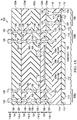
- FIG. 1B is a top down view of a disclosed TFR 290 having metal walls shown as 108 a , 108 b and 108 c that at least partially enclose the TFR 290 by walling off 3 of 4 sides of the TFR 290 .
- the metal walls each comprise a plurality of metal islands shown as 158 that may comprise M 1 , M 2 , M 3 , M 4 and M 5 connected by vias 126 that shown arranged in 2 rows that have the metal islands 158 staggered from one another.
- the metal arrangement on the top level (such as M 5 ) has metal islands 158 that each have 2 or 3 metal vias 126 therein, and the metal walls can extend from M 1 corresponding to 118 - 1 in FIG.
- the metal islands 158 can be are isolated from (shown in FIG. 1A ) or instead connected to the substrate 102 , are isolated from the functional circuitry on the IC, are proximate to the TFR 290 to not have any intervening structure between the TFR 290 and the metal islands 158 .
- FIG. 1C is a cross section view of IC shown as 170 having a TFR 290 with the at least partially surrounding 3 metal walls 108 a , 108 b and 108 c shown in FIG. 1B .
- Damage 167 to ILDs 122 b , 112 c and 122 d shown as cracks from laser trimming is shown contained within the metal walls 108 a and 108 b.
- FIG. 2A shows the in-process IC after depositing an ILD layer shown as 122 a on a substrate 102 including a semiconductor surface layer 103 having a plurality of IC die (e.g., a wafer) formed therein each including functional circuitry 180 comprising a plurality of interconnected transistors such as including MOS transistor 106 shown in FIG. 1A .
- Metal layer 118 - 1 is on PMD 114 and is under the ILD layer shown as 122 a .
- the functional circuitry (see functional circuitry 180 in FIGS. 2A-2I described below) is generally formed in the substrate 102 before forming the TFRs.
- Functional circuitry as used herein realizes and carries out a desired functionality, such as that of a digital IC (e.g., digital signal processor) or analog IC (e.g., amplifier or power converter), and in one aspect a BiCMOS (MOS and Bipolar) IC.
- a digital IC e.g., digital signal processor
- analog IC e.g., amplifier or power converter
- BiCMOS MOS and Bipolar
- the ILD layer 222 a can comprise a tetraethoxysilane TEOS-derived silicon oxide layer.
- other dielectric films can also be used for disclosed ILD layers including deposited silicon oxides such as comprising an organosilicate glass (OSG), a low-k dielectric (i.e., a smaller dielectric constant relative to silicon dioxide), a doped dielectric layer such as a fluorine-doped silica glass (FSG), or a SiN layer or its variants (e.g., SiON).
- OSG organosilicate glass
- FSG fluorine-doped silica glass
- SiN layer or its variants e.g., SiON
- FIG. 2B shows the in-process IC after depositing a TFR layer 161 on the ILD layer 122 a .
- the deposition process can comprise a direct current (DC) or radio frequency (RF) sputtering process.
- the TFR layer 161 can comprise SiCr or its alloys such as carbon containing including SiCCr, SiCOCr where C can be 1 atomic % to 50 atomic %, or NiCr or its alloys such as NiCrFe 61% Ni, 15% Cr, 24% Fe (all atomic % s), or doped polysilicon.
- the thickness of the TFR layer 161 is generally 1 nm to 50 nm, such as 2 nm to 10 nm, or about 3 to 5 nm in one specific aspect.
- FIG. 2C shows the in-process IC after depositing a hardmask layer shown as HM 162 (e.g., a TEOS derived HM layer) and then forming a pattern on the HM layer 162 .
- HM 162 e.g., a TEOS derived HM layer
- Photoresist 163 can be used to form a pattern.
- This deposition process can comprise low pressure CVD (LPCVD) at a pressure of about 300 mTorr and at a temperature of about 700° C. for a TEOS-based deposition process.
- the HM layer 162 thickness range can be 20 A to 300 A.
- FIG. 2D shows the in-process IC after etching the HM layer 162 and TFR layer 161 stopping in the ILD layer 122 a to form at least one TFR 290 that comprises the TFR layer, and then stripping of the PR layer 163 .
- the etch gases for HM layer etch in the case of silicon oxide can be Ar and CF 4 with optional Cl 2 .
- the etch gases used for etching the TFR layer 161 generally includes flowing O 2 , Cl 2 , and at least one carbon-halogen gas.
- O 2 , Cl 2 , and CF 4 with optional Ar may be used for etching SiCr.
- other gasses may also be used for etching the TFR layer such as CHF 3 , or CH 2 F 2 as a replacement for or in addition to CF 4 , and/or N 2 used as well.
- FIG. 2E shows the in-process IC after the deposition of a second ILD layer shown as ILD layer 122 b .
- the ILD layer 122 b generally comprises a deposited silicon oxide.
- FIG. 2F shows the in-process IC after forming vias 126 through the ILD 122 b and HM layer 162 to expose contacts on the TFR layer 161 , and then depositing and patterning another metal layer shown by example as a thick SiCr layer 270 (being thick as compared to TFR layer 161 , such as at least 10 times thicker, e.g., 50 A to 600 A thick).
- the thick SiCr layer 270 can be called the TFR head which is shown formed in the ILD layer 122 b .
- a plasma etch or a wet etch can be used to form vias 126 in the ILD layer 122 b for the TFR heads.
- Metal interconnects 120 contact the vias 126 and the thick SiCr layer 270 .
- FIG. 2G shows the in-process IC after depositing metal layer 118 - 2 (M 2 ) and then defining it, depositing an ILD layer 122 c , and forming vias 126 in the ILD layer 122 c .
- FIG. 2H shows the in-process IC after depositing metal layer 118 - 3 (M 3 ) and defining it, depositing an ILD layer 122 d , and forming vias 126 in the ILD layer 122 d .
- FIG. 2I shows the in-process IC after depositing metal layer 118 - 4 (M 4 ) and defining it, depositing an ILD layer 122 e , and forming vias 126 in the ILD layer 122 e .
- FIG. 2J shows the in-process IC after depositing metal layer 118 - 5 (M 5 ) and defining it on the vias 126 in the ILD layer 122 e.
- the IC can then be completed by known conventional back end of the line (BEOL) processing comprising optionally forming one or more additional metal levels including filled vias thereon to add to the metal walls to optionally include metal levels up to the top metal level.
- the top metal layer as the other metal layers can comprise aluminum or copper, or their respective alloys.
- Passivation overcoat (PO) then generally follows, followed by patterning the PO.
- the PO layer comprises at least one dielectric layer such as silicon oxide, silicon nitride, or SiON.
- the TFRs 290 are connected within the functional circuitry 180 , such as through M 2 connections that through vias and contacts reach nodes within the circuitry in the semiconductor surface layer 103 .
- the semiconductor die may include various elements therein and/or layers thereon, including barrier layers, dielectric layers, device structures, active elements and passive elements including source regions, drain regions, bit lines, bases, emitters, collectors, conductive lines, conductive vias, etc.
- the semiconductor die can be formed from a variety of processes including bipolar, Insulated Gate Bipolar Transistor (IGBT), CMOS, BiCMOS and MEMS.
- IGBT Insulated Gate Bipolar Transistor
Landscapes
- Internal Circuitry In Semiconductor Integrated Circuit Devices (AREA)
- Semiconductor Integrated Circuits (AREA)
- Metal-Oxide And Bipolar Metal-Oxide Semiconductor Integrated Circuits (AREA)
Priority Applications (6)
| Application Number | Priority Date | Filing Date | Title |
|---|---|---|---|
| US16/047,889 US10784193B2 (en) | 2018-07-27 | 2018-07-27 | IC with thin film resistor with metal walls |
| EP19841050.8A EP3830865A4 (en) | 2018-07-27 | 2019-07-25 | THIN FILM RESISTOR IC WITH METAL WALLS |
| CN201980050140.0A CN112514048B (en) | 2018-07-27 | 2019-07-25 | Integrated circuit with thin film resistor having metal wall |
| PCT/US2019/043432 WO2020023743A1 (en) | 2018-07-27 | 2019-07-25 | Ic with thin film resistor with metal walls |
| JP2021527015A JP7469815B2 (ja) | 2018-07-27 | 2019-07-25 | 金属壁を備えた薄膜抵抗器を備える集積回路 |
| US16/995,288 US11424183B2 (en) | 2018-07-27 | 2020-08-17 | IC with thin film resistor with metal walls |
Applications Claiming Priority (1)
| Application Number | Priority Date | Filing Date | Title |
|---|---|---|---|
| US16/047,889 US10784193B2 (en) | 2018-07-27 | 2018-07-27 | IC with thin film resistor with metal walls |
Related Child Applications (1)
| Application Number | Title | Priority Date | Filing Date |
|---|---|---|---|
| US16/995,288 Division US11424183B2 (en) | 2018-07-27 | 2020-08-17 | IC with thin film resistor with metal walls |
Publications (2)
| Publication Number | Publication Date |
|---|---|
| US20200035598A1 US20200035598A1 (en) | 2020-01-30 |
| US10784193B2 true US10784193B2 (en) | 2020-09-22 |
Family
ID=69178626
Family Applications (2)
| Application Number | Title | Priority Date | Filing Date |
|---|---|---|---|
| US16/047,889 Active US10784193B2 (en) | 2018-07-27 | 2018-07-27 | IC with thin film resistor with metal walls |
| US16/995,288 Active 2039-01-28 US11424183B2 (en) | 2018-07-27 | 2020-08-17 | IC with thin film resistor with metal walls |
Family Applications After (1)
| Application Number | Title | Priority Date | Filing Date |
|---|---|---|---|
| US16/995,288 Active 2039-01-28 US11424183B2 (en) | 2018-07-27 | 2020-08-17 | IC with thin film resistor with metal walls |
Country Status (4)
| Country | Link |
|---|---|
| US (2) | US10784193B2 (https=) |
| EP (1) | EP3830865A4 (https=) |
| JP (1) | JP7469815B2 (https=) |
| WO (1) | WO2020023743A1 (https=) |
Cited By (2)
| Publication number | Priority date | Publication date | Assignee | Title |
|---|---|---|---|---|
| US20210272726A1 (en) * | 2020-02-27 | 2021-09-02 | Microchip Technology Incorporated | Thin film resistor (tfr) formed in an integrated circuit device using wet etching of a dielectric cap |
| US11424183B2 (en) * | 2018-07-27 | 2022-08-23 | Texas Instruments Incorporated | IC with thin film resistor with metal walls |
Citations (10)
| Publication number | Priority date | Publication date | Assignee | Title |
|---|---|---|---|---|
| US6081014A (en) * | 1998-11-06 | 2000-06-27 | National Semiconductor Corporation | Silicon carbide chrome thin-film resistor |
| US6475873B1 (en) * | 2000-08-04 | 2002-11-05 | Maxim Integrated Products, Inc. | Method of forming laser trimmable thin-film resistors in a fully planarized integrated circuit technology |
| US20040152299A1 (en) | 2003-02-04 | 2004-08-05 | Pushpa Mahalingam | Method of forming an integrated circuit thin film resistor |
| US20060238292A1 (en) | 2005-04-11 | 2006-10-26 | Texas Instruments Incorporated | Thin film resistor and dummy fill structure and method to improve stability and reduce self-heating |
| US20090023263A1 (en) | 2007-07-18 | 2009-01-22 | Texas Instruments Incorporated | Method to manufacture a thin film resistor |
| US20150069574A1 (en) | 2013-09-06 | 2015-03-12 | Taiwan Semiconductor Manufacturing Co., Ltd. | Integrated circuit and manufacturing and method thereof |
| US9455312B2 (en) | 2012-06-15 | 2016-09-27 | Texas Instruments Incorporated | Multiple depth vias in an integrated circuit |
| WO2018004645A1 (en) | 2016-07-01 | 2018-01-04 | Intel Corporation | Thin film resistor integrated into local interconnect production |
| US20180130849A1 (en) | 2016-03-15 | 2018-05-10 | Texas Instruments Incorporated | Integrated circuit with hall effect and anisotropic magnetoresistive (amr) sensors |
| US10276648B1 (en) * | 2017-12-27 | 2019-04-30 | Texas Instruments Incorporated | Plasma treatment for thin film resistors on integrated circuits |
Family Cites Families (16)
| Publication number | Priority date | Publication date | Assignee | Title |
|---|---|---|---|---|
| JPS60136334A (ja) * | 1983-12-21 | 1985-07-19 | アドバンスト・マイクロ・デバイシズ・インコーポレイテッド | 集積回路用ヒユ−ズ素子及びその製造方法 |
| JP2821316B2 (ja) * | 1992-06-10 | 1998-11-05 | 株式会社デンソー | 半導体装置及びその製造方法 |
| US5389814A (en) * | 1993-02-26 | 1995-02-14 | International Business Machines Corporation | Electrically blowable fuse structure for organic insulators |
| JPH07153910A (ja) * | 1993-11-30 | 1995-06-16 | Sony Corp | 半導体基板上の絶縁構造 |
| JP2002237524A (ja) | 2001-02-09 | 2002-08-23 | Seiko Instruments Inc | 相補型mos半導体装置 |
| JP2005268749A (ja) | 2004-02-19 | 2005-09-29 | Ricoh Co Ltd | 半導体装置 |
| US7193292B2 (en) | 2004-12-02 | 2007-03-20 | Taiwan Semiconductor Manufacturing Co., Ltd | Fuse structure with charge protection circuit |
| JP2008021726A (ja) | 2006-07-11 | 2008-01-31 | Ricoh Co Ltd | トリミング回路及び半導体装置 |
| JP2009141266A (ja) | 2007-12-10 | 2009-06-25 | Nec Electronics Corp | 半導体装置 |
| JP5561668B2 (ja) | 2009-11-16 | 2014-07-30 | ルネサスエレクトロニクス株式会社 | 半導体装置 |
| KR101730784B1 (ko) * | 2010-11-29 | 2017-04-26 | 르네사스 일렉트로닉스 가부시키가이샤 | 반도체 장치 |
| JP6075114B2 (ja) * | 2013-02-27 | 2017-02-08 | ローム株式会社 | 半導体装置および半導体装置の製造方法 |
| JP6115277B2 (ja) | 2013-04-16 | 2017-04-19 | 富士電機株式会社 | 半導体装置 |
| US10269904B2 (en) | 2014-10-31 | 2019-04-23 | Taiwan Semiconductor Manufacturing Company Ltd. | Semiconductor structure and manufacturing method thereof |
| JP2016021586A (ja) | 2015-09-07 | 2016-02-04 | ルネサスエレクトロニクス株式会社 | 半導体装置 |
| US10784193B2 (en) * | 2018-07-27 | 2020-09-22 | Texas Instruments Incorporated | IC with thin film resistor with metal walls |
-
2018
- 2018-07-27 US US16/047,889 patent/US10784193B2/en active Active
-
2019
- 2019-07-25 JP JP2021527015A patent/JP7469815B2/ja active Active
- 2019-07-25 EP EP19841050.8A patent/EP3830865A4/en active Pending
- 2019-07-25 WO PCT/US2019/043432 patent/WO2020023743A1/en not_active Ceased
-
2020
- 2020-08-17 US US16/995,288 patent/US11424183B2/en active Active
Patent Citations (10)
| Publication number | Priority date | Publication date | Assignee | Title |
|---|---|---|---|---|
| US6081014A (en) * | 1998-11-06 | 2000-06-27 | National Semiconductor Corporation | Silicon carbide chrome thin-film resistor |
| US6475873B1 (en) * | 2000-08-04 | 2002-11-05 | Maxim Integrated Products, Inc. | Method of forming laser trimmable thin-film resistors in a fully planarized integrated circuit technology |
| US20040152299A1 (en) | 2003-02-04 | 2004-08-05 | Pushpa Mahalingam | Method of forming an integrated circuit thin film resistor |
| US20060238292A1 (en) | 2005-04-11 | 2006-10-26 | Texas Instruments Incorporated | Thin film resistor and dummy fill structure and method to improve stability and reduce self-heating |
| US20090023263A1 (en) | 2007-07-18 | 2009-01-22 | Texas Instruments Incorporated | Method to manufacture a thin film resistor |
| US9455312B2 (en) | 2012-06-15 | 2016-09-27 | Texas Instruments Incorporated | Multiple depth vias in an integrated circuit |
| US20150069574A1 (en) | 2013-09-06 | 2015-03-12 | Taiwan Semiconductor Manufacturing Co., Ltd. | Integrated circuit and manufacturing and method thereof |
| US20180130849A1 (en) | 2016-03-15 | 2018-05-10 | Texas Instruments Incorporated | Integrated circuit with hall effect and anisotropic magnetoresistive (amr) sensors |
| WO2018004645A1 (en) | 2016-07-01 | 2018-01-04 | Intel Corporation | Thin film resistor integrated into local interconnect production |
| US10276648B1 (en) * | 2017-12-27 | 2019-04-30 | Texas Instruments Incorporated | Plasma treatment for thin film resistors on integrated circuits |
Cited By (3)
| Publication number | Priority date | Publication date | Assignee | Title |
|---|---|---|---|---|
| US11424183B2 (en) * | 2018-07-27 | 2022-08-23 | Texas Instruments Incorporated | IC with thin film resistor with metal walls |
| US20210272726A1 (en) * | 2020-02-27 | 2021-09-02 | Microchip Technology Incorporated | Thin film resistor (tfr) formed in an integrated circuit device using wet etching of a dielectric cap |
| US11990257B2 (en) * | 2020-02-27 | 2024-05-21 | Microchip Technology Incorporated | Thin film resistor (TFR) formed in an integrated circuit device using wet etching of a dielectric cap |
Also Published As
| Publication number | Publication date |
|---|---|
| US11424183B2 (en) | 2022-08-23 |
| US20200381358A1 (en) | 2020-12-03 |
| WO2020023743A1 (en) | 2020-01-30 |
| JP7469815B2 (ja) | 2024-04-17 |
| JP2021531667A (ja) | 2021-11-18 |
| CN112514048A (zh) | 2021-03-16 |
| EP3830865A1 (en) | 2021-06-09 |
| US20200035598A1 (en) | 2020-01-30 |
| EP3830865A4 (en) | 2021-09-08 |
Similar Documents
| Publication | Publication Date | Title |
|---|---|---|
| US10840322B2 (en) | Thin film resistor and top plate of capacitor sharing a layer | |
| US11239230B2 (en) | IC with larger and smaller width contacts | |
| KR101751641B1 (ko) | 집적 회로 및 집적 회로의 제조 방법 | |
| JP5146504B2 (ja) | 半導体装置の製造方法 | |
| US5593925A (en) | Semiconductor device capable of preventing humidity invasion | |
| US20090023263A1 (en) | Method to manufacture a thin film resistor | |
| US8652855B2 (en) | Low resistance stacked annular contact | |
| JP4936643B2 (ja) | 半導体装置及びその製造方法 | |
| US10770538B2 (en) | Method and structure for dual sheet resistance trimmable thin film resistors | |
| JP4776199B2 (ja) | 半導体装置の製造方法 | |
| US11424183B2 (en) | IC with thin film resistor with metal walls | |
| JP4644953B2 (ja) | 半導体装置の製造方法 | |
| JP2005235995A (ja) | 半導体装置及びその製造方法 | |
| US10276648B1 (en) | Plasma treatment for thin film resistors on integrated circuits | |
| CN112838048A (zh) | 互连结构以及其制作方法 | |
| JP2005235888A (ja) | 半導体装置及びその製造方法 | |
| CN112514048B (en) | Integrated circuit with thin film resistor having metal wall | |
| JP4675050B2 (ja) | 半導体装置 | |
| TW202435422A (zh) | 帶有防氧化的薄膜電阻器 | |
| US10439020B2 (en) | In-situ plasma treatment for thin film resistors | |
| US11522043B2 (en) | IC with matched thin film resistors | |
| US20250336812A1 (en) | Thin film resistor integration within a copper interconnect | |
| JP4137040B2 (ja) | 半導体装置の製造方法 | |
| JP2005268749A (ja) | 半導体装置 | |
| JP4497975B2 (ja) | 半導体装置 |
Legal Events
| Date | Code | Title | Description |
|---|---|---|---|
| AS | Assignment |
Owner name: TEXAS INSTRUMENTS INCORPORATED, TEXAS Free format text: ASSIGNMENT OF ASSIGNORS INTEREST;ASSIGNORS:HONG, QIZHONG;GUO, HONGLIN;TIMMER, BENJAMIN JAMES;AND OTHERS;SIGNING DATES FROM 20180701 TO 20180702;REEL/FRAME:046488/0654 |
|
| FEPP | Fee payment procedure |
Free format text: ENTITY STATUS SET TO UNDISCOUNTED (ORIGINAL EVENT CODE: BIG.); ENTITY STATUS OF PATENT OWNER: LARGE ENTITY |
|
| STPP | Information on status: patent application and granting procedure in general |
Free format text: NOTICE OF ALLOWANCE MAILED -- APPLICATION RECEIVED IN OFFICE OF PUBLICATIONS |
|
| STPP | Information on status: patent application and granting procedure in general |
Free format text: NOTICE OF ALLOWANCE MAILED -- APPLICATION RECEIVED IN OFFICE OF PUBLICATIONS |
|
| STPP | Information on status: patent application and granting procedure in general |
Free format text: PUBLICATIONS -- ISSUE FEE PAYMENT VERIFIED |
|
| STCF | Information on status: patent grant |
Free format text: PATENTED CASE |
|
| MAFP | Maintenance fee payment |
Free format text: PAYMENT OF MAINTENANCE FEE, 4TH YEAR, LARGE ENTITY (ORIGINAL EVENT CODE: M1551); ENTITY STATUS OF PATENT OWNER: LARGE ENTITY Year of fee payment: 4 |