US10711368B2 - Method for producing silicon single crystal - Google Patents
Method for producing silicon single crystal Download PDFInfo
- Publication number
- US10711368B2 US10711368B2 US15/778,256 US201615778256A US10711368B2 US 10711368 B2 US10711368 B2 US 10711368B2 US 201615778256 A US201615778256 A US 201615778256A US 10711368 B2 US10711368 B2 US 10711368B2
- Authority
- US
- United States
- Prior art keywords
- monocrystalline silicon
- silicon
- power consumption
- kwh
- manufacturing
- Prior art date
- Legal status (The legal status is an assumption and is not a legal conclusion. Google has not performed a legal analysis and makes no representation as to the accuracy of the status listed.)
- Active, expires
Links
Images




Classifications
-
- C—CHEMISTRY; METALLURGY
- C30—CRYSTAL GROWTH
- C30B—SINGLE-CRYSTAL GROWTH; UNIDIRECTIONAL SOLIDIFICATION OF EUTECTIC MATERIAL OR UNIDIRECTIONAL DEMIXING OF EUTECTOID MATERIAL; REFINING BY ZONE-MELTING OF MATERIAL; PRODUCTION OF A HOMOGENEOUS POLYCRYSTALLINE MATERIAL WITH DEFINED STRUCTURE; SINGLE CRYSTALS OR HOMOGENEOUS POLYCRYSTALLINE MATERIAL WITH DEFINED STRUCTURE; AFTER-TREATMENT OF SINGLE CRYSTALS OR A HOMOGENEOUS POLYCRYSTALLINE MATERIAL WITH DEFINED STRUCTURE; APPARATUS THEREFOR
- C30B15/00—Single-crystal growth by pulling from a melt, e.g. Czochralski method
- C30B15/14—Heating of the melt or the crystallised materials
-
- C—CHEMISTRY; METALLURGY
- C30—CRYSTAL GROWTH
- C30B—SINGLE-CRYSTAL GROWTH; UNIDIRECTIONAL SOLIDIFICATION OF EUTECTIC MATERIAL OR UNIDIRECTIONAL DEMIXING OF EUTECTOID MATERIAL; REFINING BY ZONE-MELTING OF MATERIAL; PRODUCTION OF A HOMOGENEOUS POLYCRYSTALLINE MATERIAL WITH DEFINED STRUCTURE; SINGLE CRYSTALS OR HOMOGENEOUS POLYCRYSTALLINE MATERIAL WITH DEFINED STRUCTURE; AFTER-TREATMENT OF SINGLE CRYSTALS OR A HOMOGENEOUS POLYCRYSTALLINE MATERIAL WITH DEFINED STRUCTURE; APPARATUS THEREFOR
- C30B15/00—Single-crystal growth by pulling from a melt, e.g. Czochralski method
- C30B15/20—Controlling or regulating
-
- C—CHEMISTRY; METALLURGY
- C30—CRYSTAL GROWTH
- C30B—SINGLE-CRYSTAL GROWTH; UNIDIRECTIONAL SOLIDIFICATION OF EUTECTIC MATERIAL OR UNIDIRECTIONAL DEMIXING OF EUTECTOID MATERIAL; REFINING BY ZONE-MELTING OF MATERIAL; PRODUCTION OF A HOMOGENEOUS POLYCRYSTALLINE MATERIAL WITH DEFINED STRUCTURE; SINGLE CRYSTALS OR HOMOGENEOUS POLYCRYSTALLINE MATERIAL WITH DEFINED STRUCTURE; AFTER-TREATMENT OF SINGLE CRYSTALS OR A HOMOGENEOUS POLYCRYSTALLINE MATERIAL WITH DEFINED STRUCTURE; APPARATUS THEREFOR
- C30B15/00—Single-crystal growth by pulling from a melt, e.g. Czochralski method
- C30B15/36—Single-crystal growth by pulling from a melt, e.g. Czochralski method characterised by the seed, e.g. its crystallographic orientation
-
- C—CHEMISTRY; METALLURGY
- C30—CRYSTAL GROWTH
- C30B—SINGLE-CRYSTAL GROWTH; UNIDIRECTIONAL SOLIDIFICATION OF EUTECTIC MATERIAL OR UNIDIRECTIONAL DEMIXING OF EUTECTOID MATERIAL; REFINING BY ZONE-MELTING OF MATERIAL; PRODUCTION OF A HOMOGENEOUS POLYCRYSTALLINE MATERIAL WITH DEFINED STRUCTURE; SINGLE CRYSTALS OR HOMOGENEOUS POLYCRYSTALLINE MATERIAL WITH DEFINED STRUCTURE; AFTER-TREATMENT OF SINGLE CRYSTALS OR A HOMOGENEOUS POLYCRYSTALLINE MATERIAL WITH DEFINED STRUCTURE; APPARATUS THEREFOR
- C30B29/00—Single crystals or homogeneous polycrystalline material with defined structure characterised by the material or by their shape
- C30B29/02—Elements
- C30B29/06—Silicon
Definitions
- the present invention relates to a manufacturing method of monocrystalline silicon.
- a heat radiation body is raised or lowered relative to a heat shield to be positioned at an upper end of a quartz crucible, thereby inhibiting heat radiation from a silicon melt and efficiently transmitting heat of the heat radiation body to the silicon melt via the quartz crucible, so that the silicon melt can be heated to a predetermined temperature using a less electrical power.
- a temperature of an inside, expanding to a lateral upper end, of the quartz crucible can be made uniform, so that the silicon melt can be prevented from adhering on an inner circumferential surface of the upper end of the quartz crucible to inhibit occurrence of dislocation.
- a step in which the silicon melt is left still while a magnetic field is applied to the silicon melt, and subsequently a step in which the application of the magnetic field is stopped and the silicon melt is left still are conducted after a melting step of melting a polycrystalline silicon and before a pull-up step of growing monocrystalline silicon.
- cristobalite is formed on a surface of the quartz crucible in the step in which the silicon melt is left still while a magnetic field is applied to the silicon melt, and subsequently cristobalite is appropriately melted in the step in which the application of the magnetic field is stopped, so that occurrence of dislocation is inhibitable.
- Patent Literature 1 adversely requires design alternation allowing the heat radiation body to be provided therein.
- Patent Literature 2 is not applicable to the CZ method.
- An object of the invention is to provide a simple and general-purpose manufacturing method of monocrystalline silicon in which occurrence of dislocation is reducible.
- occurrence of dislocation in a straight body is reducible by starting forming a straight body of monocrystalline silicon after a power consumption of a heater configured to heat a quartz crucible becomes equal to or more than a predetermine value (i.e., 3.6 ⁇ 10 17 kJ of an energy amount given to the quartz crucible), and has achieved the invention.
- a predetermine value i.e., 3.6 ⁇ 10 17 kJ of an energy amount given to the quartz crucible
- a manufacturing method of monocrystalline silicon includes: melting silicon housed in a quartz crucible into a silicon melt by heating the quartz crucible with a heating unit; dipping a seed crystal into the silicon melt in the quartz crucible to bring the seed crystal into contact with the silicon melt; and pulling up the seed crystal to grow the monocrystalline silicon, in which, in the pulling-up, a formation of a straight body of the monocrystalline silicon is started at a power consumption of the heater being equal to or more than 10000 kWh to grow an entirety of the monocrystalline silicon.
- the manufacturing method of monocrystalline silicon further includes: temporarily-growing and melting-back to be conducted between the dipping and the pulling-up, in which in the temporarily-growing, the seed crystal in contact with the silicon melt is pulled up to grow a part of the monocrystalline silicon, and, in the melting-back, the monocrystalline silicon grown in the temporarily-growing is melted in the silicon melt.
- FIG. 1 schematically illustrates a structure of a single crystal pull-up apparatus according to an exemplary embodiment of the invention.
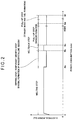
- FIG. 2 is an illustration for explaining a manufacturing method of monocrystalline silicon in the above exemplary embodiment and Example 1 of the invention.
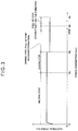
- FIG. 3 is an illustration for explaining a manufacturing method of monocrystalline silicon in a modification and Example 2 of the invention.
- FIG. 4 is an illustration for explaining a manufacturing method of monocrystalline silicon in Comparative of the invention.
- FIG. 5 shows a frequency distribution of a power consumption at the time of occurrence of dislocation in the above Comparative.
- a single-crystal pull-up apparatus 1 which is an apparatus used in the CZ method, includes a pull-up apparatus body 2 and a controller 3 as shown in FIG. 1 .
- the pull-up apparatus body 2 includes: a chamber 21 ; a crucible 22 disposed at the center of the chamber 21 ; a heater 23 (heating unit) configured to radiate heat to the crucible 22 to heat the crucible 22 ; a heat insulating cylinder 24 ; a pull-up cable 25 ; and a heat shield 26 .
- a gas inlet 21 A through which an inert gas (e.g., Ar gas) is introduced into the chamber 21 is provided at an upper portion of the chamber 21 .
- a gas outlet 21 B through which the gas inside the chamber 21 is discharged by driving a vacuum pump (not shown) is provided at the bottom of the chamber 21 .
- the controller 3 controls the inert gas to be introduced at a predetermined gas flow rate into the chamber 21 through the gas inlet 21 A provided at the upper portion of the chamber 21 .
- the introduced gas is discharged from the gas outlet 21 B provided at the bottom of the chamber 21 , so that the inert gas flows downward from an upper side in the chamber 21 .
- a pressure within the chamber 21 (furnace pressure) is controllable by the controller 3 .
- the crucible 22 is configured to melt polycrystalline silicon as a raw material of a silicon wafer to provide a silicon melt M.
- the crucible 22 is supported by a support shaft 27 rotatable at a predetermined speed and vertically movable at a predetermined speed.
- the crucible 22 includes: a bottomed cylindrical quartz crucible 221 ; and a graphite crucible 222 housing the quartz crucible 221 . It should be noted that the quartz crucible 221 and the graphite crucible 222 may have the following specification.
- Thickness from 13 mm to 35 mm
- the heater 23 is disposed outside the crucible 22 .
- the heater 23 heats the crucible 22 to melt the silicon in the crucible 22 .
- the heat insulating cylinder 24 is disposed to surround the crucible 22 and the heater 23 .
- a first end of the pull-up cable 25 is connected to a pull-up drive unit (not shown) disposed above the crucible 22 .
- a second end of the pull-up cable 25 is attached to a seed crystal SC.
- the controller 3 controls the pull-up drive unit to move up and down the pull-up cable 25 at a predetermined speed and rotate the pull-up cable 25 around its own axis.
- the heat shield 26 shields radiation heat upwardly radiated from the heater 23 .
- the controller 3 controls a gas flow rate and a furnace internal pressure in the chamber 21 , a heating temperature of an inside of the chamber 21 heated by the heater 23 , a rotation speed of each of the crucible 22 and monocrystalline silicon SM, a timing of moving up and down the seed crystal SC, and the like to manufacture the monocrystalline silicon SM.
- FIG. 2 is an illustration for explaining the manufacturing method of the monocrystalline silicon SM in the exemplary embodiment, in which the ordinate axis represents an electrical power supply to the heater 23 and the abscissa axis represents a power consumption of the heater 23 .
- the shoulder refers to a region formed continuous with the seed crystal SC and having a gradually increasing diameter
- the straight body refers to a region formed continuous with the shoulder and having an approximately uniform diameter
- the tail refers to a region formed continuous with a lower end of the straight body and having a diameter gradually reduced to zero.
- the controller 3 of the single-crystal pull-up apparatus 1 starts supplying electrical power to the heater 23 whose power consumption is zero to heat the crucible 22 , in which a polysilicon material and a dopant are received, until the power consumption reaches Wa (kWh) (Wa ⁇ 10000), thereby melting the polysilicon material and the dopant to prepare a dopant-added melt MD (the melting).
- the controller 3 introduces Ar gas at a predetermined flow rate from the gas inlet 21 A into the chamber 21 while reducing the pressure inside the chamber 21 , thereby maintaining the chamber 21 under an inert atmosphere at the reduced pressure.
- the controller 3 After the power consumption reaches Wa, the controller 3 reduces the electrical power supply to the heater 23 and lowers the pull-up cable 25 , thereby bringing the seed crystal SC into contact with the dopant-added melt MD (the dipping).
- the controller 3 pulls up the pull-up cable 25 while rotating the crucible 22 and the pull-up cable 25 in respective directions, thereby growing a part of the monocrystalline silicon SM (the temporarily-growing). It should be noted that, in the temporarily-growing, a part or an entirety of the shoulder of the monocrystalline silicon SM may be grown, or a part or an entirety of the straight body in addition to the entirety of the shoulder may be grown.
- the controller 3 increases the electrical power supply to the heater 23 to be substantially the same as that in the melting and lowers the pull-up cable 25 , thereby melting the monocrystalline silicon SM, which is grown in the temporarily-growing, in the dopant-added melt MD (the melting-back).
- the controller 3 decreases the electrical power supply to the heater 23 to be substantially the same as that in the temporarily-growing and then controls in the same manner as in the temporarily-growing, thereby growing an entirety of the monocrystalline silicon SM (the pulling-up).
- a shoulder is formed until the power consumption reaches Wd (kWh) (10000 ⁇ Wd ⁇ 12000), and subsequently a straight body and a tail are formed until the power consumption reaches Wf (kWh) (10000 ⁇ Wf).
- the formation of the straight body of the monocrystalline silicon SM is started at the power consumption of the heater 23 ranging from 10000 kWh to 12000 kWh to grow the entirety of the monocrystalline silicon SM.
- the monocrystalline silicon SM with a reduced occurrence of dislocation in the straight body is manufactured through the above process.
- a manufacturing method of the monocrystalline silicon SM as shown in FIG. 3 may be used.
- the controller 3 conducts the same melting as in the above exemplary embodiment until the power consumption of the heater 23 starting from zero reaches Wa, and subsequently the dopant-added melt MD is left still in a molten state until the power consumption reaches Wg (kWh) (Wg ⁇ 10000) without changing the electrical power supply (the leaving).
- the controller 3 decreases the electrical power supply to the heater 23 and conducts the same dipping as in the above exemplary embodiment to grow an entirety of the monocrystalline silicon SM (the pulling-up) without conducting the temporarily-growing and the melting-back subsequent to the dipping.
- the shoulder is formed until the power consumption reaches Wh (kWh) (10000 ⁇ Wh ⁇ 12000), and subsequently the straight body and the tail are formed until the power consumption reaches Wi (kWh) (10000 ⁇ Wi).
- the formation of the straight body of the monocrystalline silicon SM is started at the power consumption of the heater 23 ranging from 10000 kWh to 12000 kWh to grow the entirety of the monocrystalline silicon SM, so that occurrence of dislocation in the straight body is reducible and reduction in the productivity of the monocrystalline silicon SM is inhibitable.
- each of the temporarily-growing and the melting-back may be conducted twice or more times.
- the leaving may be conducted until the power consumption becomes equal to or more than 10000 kWh.
- each of the temporarily-growing and the melting-back may be conducted once or more times after the dipping.
- meltback simulation may be conducted in place of the leaving.
- the meltback simulation means leaving the seed crystal SC in no contact with the dopant-added melt MD while the electrical power supply to the heater 23 is controlled as shown in a period from Wa (kWh) to We (kWh) of the power consumption in FIG. 2 .
- the formation of the straight body of the monocrystalline silicon SM may start after the power consumption of the heater 23 exceeds 12000 kWh.
- a specification of each of the quartz crucible 221 and the graphite crucible 222 may be different from the above-described specification as long as an advantage of the invention is obtainable.
- the manufacturing method of the monocrystalline silicon of the invention may be applied to an MCZ method of applying a magnetic field to a melt.
- a pair of electromagnetic coils 28 are provided facing each other outside the chamber 21 with the crucible 22 interposed therebetween and as shown in chain double-dashed lines in FIG. 1 to inhibit natural convection of the silicon melt M using a traverse magnetic field in the horizontal direction.
- the same melting as in the above exemplary embodiment was conducted until the power consumption of the heater 23 starting from zero reached Wa.
- the electrical power supply to the heater 23 was decreased and the same dipping as in the exemplary embodiment was conducted to grow an entirety of the monocrystalline silicon (the pulling-up) without conducting the temporarily-growing and the melting-back subsequent to the dipping.
- the shoulder was formed until the power consumption reached Wj (kWh) (Wj ⁇ 10000), and subsequently the straight body and the tail were formed until the power consumption reached Wk (kWh) (10000 ⁇ Wk).
- a plurality of monocrystalline silicon were manufactured according to the manufacturing method of Comparative while observing whether dislocation occurred in the straight body.
- Table 1 shows conditions of occurrence of dislocation.
- FIG. 5 shows a frequency distribution of the power consumption of the heater 23 at the time of occurrence of dislocation.
- an “ALL DF ratio” in Table 1 represents a ratio of monocrystalline silicon pieces in which no occurrence of dislocation was observed in the straight body relative to all of the plurality of monocrystalline silicon pieces.
- AD (%) B 1/ B 2 ⁇ 100 (1)
- a manufacturing method of monocrystalline silicon having a high oxygen concentration is exemplified by a method of promoting incorporation of oxygen from the quartz crucible 221 into the silicon melt (dopant-added melt).
- a reaction on an inner surface of the quartz crucible 221 is promoted, where the state of the inner surface changes from an amorphous state to a brown ring and recrystallization. Since a plurality of crystalline forms are present in the inner surface of the quartz crucible 221 , a difference in thermal expansion between the crystalline forms during the change in the state of the inner surface causes a quartz piece to peel off from the inner surface.
- the quartz piece is incorporated into the monocrystalline silicon, it is considered that a stress is locally generated, whereby dislocation easily occurs.
- the reaction of the quartz crucible 221 is correlated with an oxygen concentration, a heating temperature and a heating time of the quartz crucible 221 .
- the heating temperature and the heating time of the quartz crucible 221 are correlated with the power consumption of the heater 23 (heating unit).
- the inventors inferred that the quartz piece easily peeled off by the reaction of the quartz crucible 221 at the power consumption of the heater 23 ranging from 7000 kWh to less than 10000 kWh and the incorporation of the quartz piece into the straight body caused occurrence of dislocation to concentrate on the straight body.
- the inventors made an assumption that, if the formation of the straight body was started after the power consumption of the heater 23 became equal to or more than 10000 kWh, the quartz piece would peel off before the formation of the straight body and be inhibited from peeling off after the formation of the straight body starts, so that a probability of the quartz piece to be incorporated into the straight body would become low to reduce occurrence of dislocation.
- Examples 1 and 2 below were conducted.
- the respective monocrystalline silicon were manufactured while observing in the same manner as in Comparative whether dislocation occurred in the straight body.
- Examples 1 and 2 exhibited the respective ALL DF ratios of 70% and 100%. Accordingly, it was confirmed that occurrence of dislocation in each of Examples 1 and 2 was more reducible than that in Comparative. In Example 1, dislocation occurred at the power consumption of about 17000 kWh, about 19000 kWh, and about 20000 kWh.
Landscapes
- Chemical & Material Sciences (AREA)
- Engineering & Computer Science (AREA)
- Crystallography & Structural Chemistry (AREA)
- Materials Engineering (AREA)
- Metallurgy (AREA)
- Organic Chemistry (AREA)
- Crystals, And After-Treatments Of Crystals (AREA)
- Liquid Deposition Of Substances Of Which Semiconductor Devices Are Composed (AREA)
Applications Claiming Priority (3)
| Application Number | Priority Date | Filing Date | Title |
|---|---|---|---|
| JP2015231072A JP6515791B2 (ja) | 2015-11-26 | 2015-11-26 | シリコン単結晶の製造方法 |
| JP2015-231072 | 2015-11-26 | ||
| PCT/JP2016/079664 WO2017090325A1 (ja) | 2015-11-26 | 2016-10-05 | シリコン単結晶の製造方法 |
Publications (2)
| Publication Number | Publication Date |
|---|---|
| US20180355508A1 US20180355508A1 (en) | 2018-12-13 |
| US10711368B2 true US10711368B2 (en) | 2020-07-14 |
Family
ID=58763792
Family Applications (1)
| Application Number | Title | Priority Date | Filing Date |
|---|---|---|---|
| US15/778,256 Active 2037-02-01 US10711368B2 (en) | 2015-11-26 | 2016-10-05 | Method for producing silicon single crystal |
Country Status (7)
| Country | Link |
|---|---|
| US (1) | US10711368B2 (ja) |
| JP (1) | JP6515791B2 (ja) |
| KR (1) | KR102056661B1 (ja) |
| CN (1) | CN108291328B (ja) |
| DE (1) | DE112016005411B4 (ja) |
| TW (1) | TWI622671B (ja) |
| WO (1) | WO2017090325A1 (ja) |
Families Citing this family (1)
| Publication number | Priority date | Publication date | Assignee | Title |
|---|---|---|---|---|
| JP2024147945A (ja) * | 2023-04-04 | 2024-10-17 | 株式会社Sumco | シリコン単結晶の製造方法、および、シリコン単結晶製造装置 |
Citations (11)
| Publication number | Priority date | Publication date | Assignee | Title |
|---|---|---|---|---|
| JPH04198087A (ja) | 1990-11-28 | 1992-07-17 | Osaka Titanium Co Ltd | 単結晶引上げ方法 |
| JPH06305878A (ja) | 1993-04-26 | 1994-11-01 | Kawasaki Steel Corp | シリコン単結晶製造装置 |
| JPH07133185A (ja) | 1993-11-08 | 1995-05-23 | Japan Energy Corp | 単結晶の製造方法 |
| JPH11255577A (ja) | 1998-03-11 | 1999-09-21 | Mitsubishi Materials Silicon Corp | シリコン単結晶の引上げ装置及びその引上げ方法 |
| WO2002027076A1 (fr) | 2000-09-26 | 2002-04-04 | Shin-Etsu Handotai Co.,Ltd. | Appareil et procede de production d'un mono-cristal semi-conducteur |
| JP2002226293A (ja) | 2000-11-30 | 2002-08-14 | Memc Japan Ltd | シリコン単結晶の成長方法 |
| JP2006069874A (ja) | 2004-09-06 | 2006-03-16 | Toshiba Ceramics Co Ltd | シリコン単結晶の製造方法 |
| US20080081767A1 (en) * | 2004-12-28 | 2008-04-03 | Tateho Chemical Industries Co., Ltd. | Magnesium Oxide Single Crystal Having Controlled Crystallinity and Method for Producing the Same, and Substrate Using the Single Crystal |
| JP2012082121A (ja) | 2010-10-15 | 2012-04-26 | Shin Etsu Handotai Co Ltd | シリコン単結晶の製造方法 |
| JP2012091942A (ja) | 2010-10-22 | 2012-05-17 | Sumco Corp | シリコン単結晶引き上げ装置及びシリコン単結晶の製造方法 |
| JP2015151283A (ja) | 2014-02-12 | 2015-08-24 | 信越半導体株式会社 | シリコン単結晶製造装置 |
Family Cites Families (1)
| Publication number | Priority date | Publication date | Assignee | Title |
|---|---|---|---|---|
| JP5163101B2 (ja) * | 2007-12-25 | 2013-03-13 | 信越半導体株式会社 | 単結晶製造装置および製造方法 |
-
2015
- 2015-11-26 JP JP2015231072A patent/JP6515791B2/ja active Active
-
2016
- 2016-10-05 KR KR1020187014309A patent/KR102056661B1/ko active Active
- 2016-10-05 WO PCT/JP2016/079664 patent/WO2017090325A1/ja not_active Ceased
- 2016-10-05 DE DE112016005411.4T patent/DE112016005411B4/de active Active
- 2016-10-05 CN CN201680068989.7A patent/CN108291328B/zh active Active
- 2016-10-05 US US15/778,256 patent/US10711368B2/en active Active
- 2016-10-12 TW TW105132822A patent/TWI622671B/zh active
Patent Citations (12)
| Publication number | Priority date | Publication date | Assignee | Title |
|---|---|---|---|---|
| JPH04198087A (ja) | 1990-11-28 | 1992-07-17 | Osaka Titanium Co Ltd | 単結晶引上げ方法 |
| JPH06305878A (ja) | 1993-04-26 | 1994-11-01 | Kawasaki Steel Corp | シリコン単結晶製造装置 |
| JPH07133185A (ja) | 1993-11-08 | 1995-05-23 | Japan Energy Corp | 単結晶の製造方法 |
| JPH11255577A (ja) | 1998-03-11 | 1999-09-21 | Mitsubishi Materials Silicon Corp | シリコン単結晶の引上げ装置及びその引上げ方法 |
| WO2002027076A1 (fr) | 2000-09-26 | 2002-04-04 | Shin-Etsu Handotai Co.,Ltd. | Appareil et procede de production d'un mono-cristal semi-conducteur |
| JP3979291B2 (ja) | 2000-09-26 | 2007-09-19 | 信越半導体株式会社 | 半導体単結晶の製造装置並びに製造方法 |
| JP2002226293A (ja) | 2000-11-30 | 2002-08-14 | Memc Japan Ltd | シリコン単結晶の成長方法 |
| JP2006069874A (ja) | 2004-09-06 | 2006-03-16 | Toshiba Ceramics Co Ltd | シリコン単結晶の製造方法 |
| US20080081767A1 (en) * | 2004-12-28 | 2008-04-03 | Tateho Chemical Industries Co., Ltd. | Magnesium Oxide Single Crystal Having Controlled Crystallinity and Method for Producing the Same, and Substrate Using the Single Crystal |
| JP2012082121A (ja) | 2010-10-15 | 2012-04-26 | Shin Etsu Handotai Co Ltd | シリコン単結晶の製造方法 |
| JP2012091942A (ja) | 2010-10-22 | 2012-05-17 | Sumco Corp | シリコン単結晶引き上げ装置及びシリコン単結晶の製造方法 |
| JP2015151283A (ja) | 2014-02-12 | 2015-08-24 | 信越半導体株式会社 | シリコン単結晶製造装置 |
Non-Patent Citations (3)
| Title |
|---|
| Notice of Allowance in Korean Patent Application No. 10-2018-7014309, dated Nov. 28, 2019; and partial English-language translation thereof. |
| Office Action issued in Japan Counterpart Patent Appl. No. 2015-231072, dated Mar. 19, 2019, along with an English translation thereof. |
| Official Communication issued in Japan Patent Application No. PCT/JP2016/079664, dated Nov. 8, 2016. |
Also Published As
| Publication number | Publication date |
|---|---|
| US20180355508A1 (en) | 2018-12-13 |
| TWI622671B (zh) | 2018-05-01 |
| CN108291328A (zh) | 2018-07-17 |
| KR20180072777A (ko) | 2018-06-29 |
| TW201726985A (zh) | 2017-08-01 |
| CN108291328B (zh) | 2020-11-17 |
| KR102056661B1 (ko) | 2019-12-17 |
| WO2017090325A1 (ja) | 2017-06-01 |
| DE112016005411B4 (de) | 2023-03-16 |
| JP2017095323A (ja) | 2017-06-01 |
| JP6515791B2 (ja) | 2019-05-22 |
| DE112016005411T5 (de) | 2018-08-02 |
Similar Documents
| Publication | Publication Date | Title |
|---|---|---|
| US11702760B2 (en) | N-type silicon single crystal production method, n-type silicon single crystal ingot, silicon wafer, and epitaxial silicon wafer | |
| US7588638B2 (en) | Single crystal pulling apparatus | |
| US10233564B2 (en) | Manufacturing method of monocrystalline silicon and monocrystalline silicon | |
| US10329686B2 (en) | Method for producing single crystal | |
| US20160208408A1 (en) | Upper heat shielding body, ingot growing apparatus having the same and ingot growing method using the same | |
| US20200135460A1 (en) | Single crystal silicon production method, epitaxial silicon wafer production method, single crystal silicon, and epitaxial silicon wafer | |
| US10494734B2 (en) | Method for producing silicon single crystals | |
| US20170362736A1 (en) | Apparatus and method for growing silicon single crystal ingot | |
| JP2010024120A (ja) | シリコン単結晶およびその育成方法 | |
| CN107109686A (zh) | 用于制造单晶硅锭的方法、以及通过该制备方法制备的单晶硅锭 | |
| CN119082841A (zh) | 一种顶部籽晶法生长碳化硅晶体的装置及生长方法 | |
| US10711368B2 (en) | Method for producing silicon single crystal | |
| US20090293803A1 (en) | Method of growing silicon single crystals | |
| CN109154101B (zh) | 生产单晶硅半导体晶片的方法、生产单晶硅半导体晶片的设备和单晶硅半导体晶片 | |
| JP2009292662A (ja) | シリコン単結晶育成における肩形成方法 | |
| JP5489064B2 (ja) | シリコン単結晶の育成方法 | |
| JP2016204231A (ja) | シリコン単結晶の製造方法 | |
| KR100946558B1 (ko) | 커스프 자기장을 이용한 반도체 단결정 제조장치 및 방법 | |
| JP2004262723A (ja) | 単結晶引上装置及び単結晶引上方法 | |
| US20200199776A1 (en) | Method for producing silicon single crystal | |
| JP2014058414A (ja) | 評価用シリコン単結晶の製造方法 | |
| WO2005075715A1 (ja) | 単結晶半導体の製造方法 | |
| JP2021098622A (ja) | 単結晶シリコンインゴットの製造方法 | |
| CN110983439A (zh) | 原料供给方法和单晶硅的制造方法 | |
| KR101193678B1 (ko) | 대구경 단결정 잉곳 제조방법 |
Legal Events
| Date | Code | Title | Description |
|---|---|---|---|
| AS | Assignment |
Owner name: SUMCO CORPORATION, JAPAN Free format text: ASSIGNMENT OF ASSIGNORS INTEREST;ASSIGNOR:KIM, TEGI;REEL/FRAME:045879/0280 Effective date: 20180409 |
|
| FEPP | Fee payment procedure |
Free format text: ENTITY STATUS SET TO UNDISCOUNTED (ORIGINAL EVENT CODE: BIG.); ENTITY STATUS OF PATENT OWNER: LARGE ENTITY |
|
| STPP | Information on status: patent application and granting procedure in general |
Free format text: DOCKETED NEW CASE - READY FOR EXAMINATION |
|
| STPP | Information on status: patent application and granting procedure in general |
Free format text: NON FINAL ACTION MAILED |
|
| STPP | Information on status: patent application and granting procedure in general |
Free format text: RESPONSE TO NON-FINAL OFFICE ACTION ENTERED AND FORWARDED TO EXAMINER |
|
| STPP | Information on status: patent application and granting procedure in general |
Free format text: NOTICE OF ALLOWANCE MAILED -- APPLICATION RECEIVED IN OFFICE OF PUBLICATIONS |
|
| STPP | Information on status: patent application and granting procedure in general |
Free format text: PUBLICATIONS -- ISSUE FEE PAYMENT VERIFIED |
|
| STCF | Information on status: patent grant |
Free format text: PATENTED CASE |
|
| MAFP | Maintenance fee payment |
Free format text: PAYMENT OF MAINTENANCE FEE, 4TH YEAR, LARGE ENTITY (ORIGINAL EVENT CODE: M1551); ENTITY STATUS OF PATENT OWNER: LARGE ENTITY Year of fee payment: 4 |