US10686417B2 - Radio frequency amplifier - Google Patents
Radio frequency amplifier Download PDFInfo
- Publication number
- US10686417B2 US10686417B2 US15/520,378 US201515520378A US10686417B2 US 10686417 B2 US10686417 B2 US 10686417B2 US 201515520378 A US201515520378 A US 201515520378A US 10686417 B2 US10686417 B2 US 10686417B2
- Authority
- US
- United States
- Prior art keywords
- data stream
- delta
- modulator
- sigma
- signal
- Prior art date
- Legal status (The legal status is an assumption and is not a legal conclusion. Google has not performed a legal analysis and makes no representation as to the accuracy of the status listed.)
- Active, expires
Links
- 238000012545 processing Methods 0.000 claims abstract description 58
- 239000000872 buffer Substances 0.000 claims description 26
- 238000000034 method Methods 0.000 claims description 19
- 238000007493 shaping process Methods 0.000 claims description 9
- 230000036962 time dependent Effects 0.000 claims description 7
- 230000001419 dependent effect Effects 0.000 claims description 3
- 230000003139 buffering effect Effects 0.000 claims description 2
- 230000006870 function Effects 0.000 description 30
- 230000003321 amplification Effects 0.000 description 13
- 238000003199 nucleic acid amplification method Methods 0.000 description 13
- 238000004891 communication Methods 0.000 description 9
- 230000000875 corresponding effect Effects 0.000 description 8
- 230000008901 benefit Effects 0.000 description 7
- 238000010586 diagram Methods 0.000 description 7
- 238000013459 approach Methods 0.000 description 5
- 238000005516 engineering process Methods 0.000 description 5
- 238000005562 fading Methods 0.000 description 5
- 238000012546 transfer Methods 0.000 description 5
- 101100445834 Drosophila melanogaster E(z) gene Proteins 0.000 description 4
- XUIMIQQOPSSXEZ-UHFFFAOYSA-N Silicon Chemical compound [Si] XUIMIQQOPSSXEZ-UHFFFAOYSA-N 0.000 description 4
- 230000000694 effects Effects 0.000 description 4
- 238000012986 modification Methods 0.000 description 4
- 230000004048 modification Effects 0.000 description 4
- 229910052710 silicon Inorganic materials 0.000 description 4
- 239000010703 silicon Substances 0.000 description 4
- 238000004088 simulation Methods 0.000 description 4
- 230000003595 spectral effect Effects 0.000 description 4
- 230000009467 reduction Effects 0.000 description 3
- 230000004044 response Effects 0.000 description 3
- 238000001228 spectrum Methods 0.000 description 3
- 230000009286 beneficial effect Effects 0.000 description 2
- 239000000969 carrier Substances 0.000 description 2
- 238000001914 filtration Methods 0.000 description 2
- 230000008569 process Effects 0.000 description 2
- 239000004065 semiconductor Substances 0.000 description 2
- 230000001052 transient effect Effects 0.000 description 2
- 239000010752 BS 2869 Class D Substances 0.000 description 1
- 238000004458 analytical method Methods 0.000 description 1
- 230000005540 biological transmission Effects 0.000 description 1
- 230000001413 cellular effect Effects 0.000 description 1
- 230000000295 complement effect Effects 0.000 description 1
- 238000004590 computer program Methods 0.000 description 1
- 230000002596 correlated effect Effects 0.000 description 1
- 238000000354 decomposition reaction Methods 0.000 description 1
- 230000008030 elimination Effects 0.000 description 1
- 238000003379 elimination reaction Methods 0.000 description 1
- 230000001747 exhibiting effect Effects 0.000 description 1
- 230000005669 field effect Effects 0.000 description 1
- 230000007774 longterm Effects 0.000 description 1
- 238000005070 sampling Methods 0.000 description 1
- 238000012360 testing method Methods 0.000 description 1
Images


Classifications
-
- H—ELECTRICITY
- H03—ELECTRONIC CIRCUITRY
- H03M—CODING; DECODING; CODE CONVERSION IN GENERAL
- H03M3/00—Conversion of analogue values to or from differential modulation
- H03M3/30—Delta-sigma modulation
- H03M3/39—Structural details of delta-sigma modulators, e.g. incremental delta-sigma modulators
-
- H—ELECTRICITY
- H03—ELECTRONIC CIRCUITRY
- H03F—AMPLIFIERS
- H03F3/00—Amplifiers with only discharge tubes or only semiconductor devices as amplifying elements
- H03F3/20—Power amplifiers, e.g. Class B amplifiers, Class C amplifiers
- H03F3/21—Power amplifiers, e.g. Class B amplifiers, Class C amplifiers with semiconductor devices only
- H03F3/217—Class D power amplifiers; Switching amplifiers
- H03F3/2175—Class D power amplifiers; Switching amplifiers using analogue-digital or digital-analogue conversion
-
- H—ELECTRICITY
- H03—ELECTRONIC CIRCUITRY
- H03F—AMPLIFIERS
- H03F3/00—Amplifiers with only discharge tubes or only semiconductor devices as amplifying elements
- H03F3/189—High-frequency amplifiers, e.g. radio frequency amplifiers
- H03F3/19—High-frequency amplifiers, e.g. radio frequency amplifiers with semiconductor devices only
-
- H—ELECTRICITY
- H03—ELECTRONIC CIRCUITRY
- H03M—CODING; DECODING; CODE CONVERSION IN GENERAL
- H03M3/00—Conversion of analogue values to or from differential modulation
- H03M3/30—Delta-sigma modulation
-
- H—ELECTRICITY
- H03—ELECTRONIC CIRCUITRY
- H03M—CODING; DECODING; CODE CONVERSION IN GENERAL
- H03M3/00—Conversion of analogue values to or from differential modulation
- H03M3/30—Delta-sigma modulation
- H03M3/39—Structural details of delta-sigma modulators, e.g. incremental delta-sigma modulators
- H03M3/412—Structural details of delta-sigma modulators, e.g. incremental delta-sigma modulators characterised by the number of quantisers and their type and resolution
- H03M3/422—Structural details of delta-sigma modulators, e.g. incremental delta-sigma modulators characterised by the number of quantisers and their type and resolution having one quantiser only
-
- H—ELECTRICITY
- H03—ELECTRONIC CIRCUITRY
- H03M—CODING; DECODING; CODE CONVERSION IN GENERAL
- H03M3/00—Conversion of analogue values to or from differential modulation
- H03M3/30—Delta-sigma modulation
- H03M3/458—Analogue/digital converters using delta-sigma modulation as an intermediate step
- H03M3/466—Multiplexed conversion systems
- H03M3/468—Interleaved, i.e. using multiple converters or converter parts for one channel, e.g. using Hadamard codes, pi-delta-sigma converters
- H03M3/47—Interleaved, i.e. using multiple converters or converter parts for one channel, e.g. using Hadamard codes, pi-delta-sigma converters using time-division multiplexing
-
- H—ELECTRICITY
- H03—ELECTRONIC CIRCUITRY
- H03M—CODING; DECODING; CODE CONVERSION IN GENERAL
- H03M3/00—Conversion of analogue values to or from differential modulation
- H03M3/30—Delta-sigma modulation
- H03M3/50—Digital/analogue converters using delta-sigma modulation as an intermediate step
-
- H—ELECTRICITY
- H03—ELECTRONIC CIRCUITRY
- H03M—CODING; DECODING; CODE CONVERSION IN GENERAL
- H03M7/00—Conversion of a code where information is represented by a given sequence or number of digits to a code where the same, similar or subset of information is represented by a different sequence or number of digits
- H03M7/30—Compression; Expansion; Suppression of unnecessary data, e.g. redundancy reduction
- H03M7/3002—Conversion to or from differential modulation
- H03M7/3004—Digital delta-sigma modulation
- H03M7/3015—Structural details of digital delta-sigma modulators
-
- H—ELECTRICITY
- H03—ELECTRONIC CIRCUITRY
- H03F—AMPLIFIERS
- H03F2200/00—Indexing scheme relating to amplifiers
- H03F2200/171—A filter circuit coupled to the output of an amplifier
-
- H—ELECTRICITY
- H03—ELECTRONIC CIRCUITRY
- H03F—AMPLIFIERS
- H03F2200/00—Indexing scheme relating to amplifiers
- H03F2200/331—Sigma delta modulation being used in an amplifying circuit
-
- H—ELECTRICITY
- H03—ELECTRONIC CIRCUITRY
- H03F—AMPLIFIERS
- H03F2200/00—Indexing scheme relating to amplifiers
- H03F2200/451—Indexing scheme relating to amplifiers the amplifier being a radio frequency amplifier
-
- H—ELECTRICITY
- H03—ELECTRONIC CIRCUITRY
- H03M—CODING; DECODING; CODE CONVERSION IN GENERAL
- H03M3/00—Conversion of analogue values to or from differential modulation
- H03M3/30—Delta-sigma modulation
- H03M3/458—Analogue/digital converters using delta-sigma modulation as an intermediate step
- H03M3/466—Multiplexed conversion systems
-
- H—ELECTRICITY
- H04—ELECTRIC COMMUNICATION TECHNIQUE
- H04B—TRANSMISSION
- H04B1/00—Details of transmission systems, not covered by a single one of groups H04B3/00 - H04B13/00; Details of transmission systems not characterised by the medium used for transmission
- H04B1/02—Transmitters
- H04B1/04—Circuits
-
- H—ELECTRICITY
- H04—ELECTRIC COMMUNICATION TECHNIQUE
- H04B—TRANSMISSION
- H04B1/00—Details of transmission systems, not covered by a single one of groups H04B3/00 - H04B13/00; Details of transmission systems not characterised by the medium used for transmission
- H04B1/06—Receivers
- H04B1/16—Circuits
-
- H—ELECTRICITY
- H04—ELECTRIC COMMUNICATION TECHNIQUE
- H04B—TRANSMISSION
- H04B1/00—Details of transmission systems, not covered by a single one of groups H04B3/00 - H04B13/00; Details of transmission systems not characterised by the medium used for transmission
- H04B1/02—Transmitters
- H04B1/04—Circuits
- H04B2001/0408—Circuits with power amplifiers
Definitions
- the present invention relates to an amplifier for amplifying radio frequency (RF) signals.
- the invention has particular but not exclusive relevance to delta-sigma amplifiers for wireless communications systems and devices thereof operating according to the Long Term Evolution (LTE) technologies defined by the 3 rd Generation Partnership Project (3GPP).
- LTE Long Term Evolution
- 3GPP 3 rd Generation Partnership Project
- Linear refers to the ability of an amplifier to produce output signals that are accurate copies of the input signal (generally) at increased power levels.
- Linear amplification is essential for non-constant envelope signals such as OFDM to prevent the creation of unwanted in-band interference signals.
- Linear amplification must be achieved for peak signal power, not just for average signal power. Peak signal power can be up to 10 dB higher than average signal power for OFDM signals.
- Linearity is usually achieved by backing-off the amplifier's power level to below its maximum (and most efficient) region to a region exhibiting a more linear amplification for both the average and the expected maximum signal level.
- this effectively results in a reduction of the amplifier's overall power efficiency compared to the case when the amplifier operates near its peak power level most of the time. Consequently, linear RF amplifiers typically have a power efficiency of less than 10%.
- S-class amplifier uses delta-sigma modulation to generate directly an amplified RF signal. Since S-class amplifiers use field effect transistors (e.g. metal-oxide-semiconductor, ‘MOS’ transistors) (or other transistors) for generating a modulated signal, and since transistors are either turned on or off, efficiency of S-class amplifiers can theoretically approach 100%.
- MOS metal-oxide-semiconductor
- delta-sigma modulation signal frequency also referred to as the delta sigma bitstream rate
- the delta-sigma modulation signal frequency must be at least twice (typically four times) the carrier frequency of the signal to be amplified (due to the Nyquist sampling theorem).
- delta-sigma modulation has a single-cycle feedback loop, which consists of several steps including: summation of the input signal with a loop-filtered error signal; quantisation (usually as truncation of a fixed point binary number); and error feedback into a loop filter.
- the logic in the delta-sigma modulator must be computed at the delta sigma bitstream rate. Since cellular signals may be transmitted at around 1 GHz (typically in the range of 800-900 MHz for applications such as LTE) or even above 1 GHz, the delta-sigma modulation signal must be generated at several GHz. This effectively means that the delta-sigma modulator logic must operate at an impractically high rate, which would inhibit feasible and/or economical implementation of delta-sigma amplification for radio frequency signals used in LTE systems and/or the like.
- preferred embodiments of the present invention aim to provide methods and apparatus which address or at least partially deal with the above issues.
- delta-sigma ( ⁇ ) amplifier refers to any communications device employing a delta-sigma modulation technology for amplification of a transmitted signal (e.g. a data burst). It will also be appreciated that the technology described herein can be implemented on any (mobile and/or generally stationary) communications device that can communicate with another communications device and/or a communications network.
- the invention provides a modulator circuit comprising: means for receiving an input data stream having a carrier frequency (which may be zero); means for splitting the input data stream into a plurality of data stream portions; a plurality of signal processing branches, each signal processing branch comprising means for performing a delta-sigma modulation of a respective data stream portion of said plurality of data stream portions in order to generate a modulated signal; and means for combining the respective modulated signal from each of said plurality of signal processing branches to form an output signal, and for outputting said output signal at said carrier frequency.
- a carrier frequency which may be zero
- each signal processing branch comprising means for performing a delta-sigma modulation of a respective data stream portion of said plurality of data stream portions in order to generate a modulated signal
- the means for receiving an input data stream, the means for splitting, the plurality of signal processing branches, and the means for combining and for outputting may all form part of a first circuit portion and the output signal of said first circuit portion may comprise a first output signal.
- the modulator circuit may further comprise: a second circuit portion, the second circuit portion comprising: further means for receiving the input data stream; further means for splitting the input data stream into a further plurality of data stream portions; a further plurality of signal processing branches, each further signal processing branch comprising respective further means for performing a delta-sigma modulation of a respective further data stream portion of said plurality of further data stream portions in order to generate a further modulated signal; and further means for combining the respective further modulated signal from each of said plurality of further signal processing branches to form a further output signal, and for outputting said further output signal at said carrier frequency as a second output signal; and means for generating a combined output signal from said first output signal and said second output signal, wherein said generating comprises applying a respective window function to each
- the applying of a respective window function may comprise applying a respective time dependent weight to each of said first and said second output signals.
- the respective time dependent weights applied to said first and said second output signals may sum together to give a constant (e.g. 1).
- the respective time dependent weights may vary with time in the manner of a substantially triangular waveform.
- the substantially triangular waveform may comprise a substantially continuous triangular waveform in which the sides of the triangular wave are substantially linear.
- the respective time dependent weights may vary with time in the manner of a stepped waveform.
- the respective time dependent weights may vary with time in the manner of a stepped but generally triangular waveform.
- the plurality of data stream portions of the first circuit portion may be offset in time compared to the further plurality of data stream portions of the second circuit portion.
- the weight applied to the first output signal may be substantially zero at a start and end of each data stream portion of said plurality of data stream portions, and wherein a weight applied to said second output signal is substantially zero at a start and end of each data stream portion of said further plurality of data stream portions.
- the invention provides an amplifier circuit comprising the above described modulator circuit.
- the invention provides a method performed by a modulator circuit comprising a plurality of signal processing branches having means for performing a delta-sigma modulation, the method comprising: receiving an input data stream having a carrier frequency; splitting the input data stream into a plurality of data stream portions; in each of said plurality of signal processing branches, performing a delta-sigma modulation of a respective data stream portion of said plurality of data stream portions in order to generate a modulated signal; combining the respective modulated signal from each of said plurality of signal processing branches to form an output signal; and outputting said output signal at said carrier frequency.
- aspects of the invention extend to corresponding computer program products such as computer readable storage media having instructions stored thereon which are operable to program a programmable processor to carry out a method as described in the aspects and possibilities set out above or recited in the claims and/or to program a suitably adapted computer to provide the apparatus recited in any of the claims.
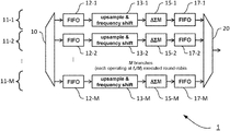
- FIG. 1 illustrates schematically a delta-sigma modulator for processing concatenated independent blocks
- FIG. 2 is a schematic diagram of an exemplary radio frequency delta-sigma amplifier circuit which includes the delta-sigma modulator shown in FIG. 1 ;
- FIG. 3 is a schematic diagram illustrating an exemplary error feedback delta-sigma modulator forming part of the delta-sigma modulator shown in FIG. 1 ;
- FIG. 4 illustrates an exemplary noise transfer function for bandpass delta-sigma amplifier in accordance with embodiments of the present invention
- FIG. 5 is an exemplary timing snapshot illustrating the operation of a branch of a delta-sigma modulator employing concatenated independent blocks
- FIG. 6 is an exemplary power spectral density diagram illustrating simulation results for different block lengths
- FIGS. 7 a and 7 b illustrate an exemplary window function and a possible implementation thereof
- FIG. 8 is an exemplary power spectral density diagram illustrating simulation results when employing the window function shown in FIG. 7 a;
- FIGS. 9 a and 9 b illustrate another exemplary window function and a possible implementation thereof.
- FIG. 10 is an exemplary power spectral density diagram illustrating simulation results when employing the window function shown in FIG. 9 a.
- FIG. 1 schematically illustrates a delta-sigma modulator circuit 1 for processing RF signals.
- the delta-sigma modulator circuit 1 comprises a so-called Donoghue-Phillips-Tan delta-sigma modulator (hereafter referred to as a DPT modulator 1 ) forming part of an exemplary (S-Class) RF amplifier 2 .
- the RF amplifier 2 includes, amongst others, the DPT modulator 1 , transistor switching circuits and a bandpass filter.
- modulation of a transmit signal is achieved using concatenated independent blocks (CIBs). Specifically, each transmit burst (received at demultiplexer 10 ) is split into a number of consecutive blocks of output symbols and for each block upsampling, frequency shift and modulation is performed independently.
- CBs concatenated independent blocks
- processing of the consecutive blocks is realised by demultiplexing, in a “round-robin” manner, the blocks of input baseband samples to a number of branches 11 - 1 to 11 -M at the demultiplexer 10 .
- Each branch 11 comprises a respective: input buffer 12 - 1 to 12 -M; optionally an independent upsampler and frequency shift portion 13 - 1 to 13 -M; delta-sigma modulator portion 15 - 1 to 15 -M (denoted ‘ ⁇ M’ in FIG. 1 ); and output buffer 17 - 1 to 17 -M.
- Each input buffer 12 and each output buffer 17 comprises a suitable ‘first-in-first-out’ (FIFO) input buffer.
- Each upsampler and frequency shift portion 13 may comprise, for example, a finite impulse response (FIR) filter, cascaded integrator-comb (CIC) filters, oscillator and a frequency mixer, although it will be appreciated that other types of filters and/or other filter combinations and frequency shifters may also be used. It will also be appreciated that the upsampler and frequency shift portions 13 - 1 to 13 -M are optional and may be omitted.
- FIR finite impulse response
- CIC cascaded integrator-comb
- Each block of symbols from the demultiplexer 10 are buffered in the input buffer 12 of a respective branch 11 for processing that block.
- Symbols are taken from input buffer in a FIFO manner and are (optionally) upsampled and frequency shifted by the corresponding upsampler and frequency shift portion 13 to provide an upsampled and frequency shifted output.
- the upsampled and frequency shifted output is modulated by the corresponding delta-sigma modulator portion 15 .
- the modulated output from each delta-sigma modulator portion 15 i.e. the signal corresponding to the block processed by that branch 11
- the contents of the output buffers 17 are multiplexed into an output signal at a multiplexer 20 .
- each part of the multiplexed signal is generated ‘offline’, in a round-robin manner, via a different branch 11 , before being re-combined (multiplexed) at the output multiplexer 20 of the DPT modulator circuit 1 to re-combine the signals from the respective branches into a single modulated signal stream.
- the re-combined signal is sent to appropriate transmit circuitry (e.g. a switching amplifier and bandpass filter, shown in FIG. 2 ) for transmission at the required power level.
- each branch 11 can operate at a relatively low rate of f s /M, where ‘f s ’ is the delta-sigma bitstream rate (e.g. a minimum of twice the carrier frequency), and ‘M’ is the number of branches.
- f s is the delta-sigma bitstream rate (e.g. a minimum of twice the carrier frequency)
- M is the number of branches.
- the resulting delta-sigma amplification circuit 2 (including the DPT modulator 1 ) is able to achieve the necessary parallelism and linearity for high frequency applications such as amplification of radio frequency signals (e.g. OFDM).
- radio frequency signals e.g. OFDM
- FIGS. 1 to 6 A more detailed description will now be given (with reference to FIGS. 1 to 6 ) of an exemplary delta-sigma modulation technique implemented in accordance with an embodiment of the present invention.
- FIG. 2 illustrates an exemplary S-class RF amplifier 2 which includes the DPT modulator 1 shown in FIG. 1 .
- the amplifier 2 can receive (at its input) a digital (e.g. OFDM) signal which may be at baseband, at an intermediate frequency or at the carrier frequency.
- the digital signal is optionally upsampled and frequency shifted, and then modulated by the DPT modulator 1 .
- the modulated input signal is sent through a complementary metal-oxide-semiconductor (CMOS) or other type of transistor circuit, which results in an amplified output signal (denoted ‘Amplified Output’ in FIG. 2 ) being generated at the output of the transistor circuit.
- CMOS complementary metal-oxide-semiconductor
- an output signal substantially corresponding to a copy of the input signal, albeit at increased power level and shifted frequency
- FIG. 3 illustrates an exemplary delta-sigma error feedback model that may be used to help understand operation of the delta-sigma modulator ( ⁇ M) portion 15 shown in FIG. 1 .
- ⁇ M delta-sigma modulator
- a delta-sigma modulator is effectively an infinite impulse response (IIR) filter, thus its current state depends on an infinite history of previous states (i.e. it has an impulse response which does not become zero past a certain point, but continues indefinitely).
- the delta-sigma modulator also has a non-linearity in its feedback loop meaning that standard linear time-invariant (LTI) analysis for the delta-sigma modulator fails.
- LTI linear time-invariant
- the quantiser shown in FIG. 3 may be considered, conceptually, to be replaced with the addition of a quantisation error, +E(z), which equals the difference between the quantiser's input and its output (T output ⁇ T input ).
- V ( z ) NTF ( z ) ⁇ E ( z )+ U ( z )
- U(z) is the input signal
- V(z) is the output signal
- NTF(z) is a noise transfer function equal to 1 ⁇ H(z) (H(z) being the feedback function as shown in FIG. 3 )
- E(z) is the quantisation error.
- the noise transfer function (NTF(z)) is designed to dump noise energy into regions of spectrum outside a band of interest around ‘U(z)’. Any signal (noise) falling into such outside or “don't care” regions may be removed from further processing by applying an appropriate filter to the signal (e.g. a bandpass filter, a pair of appropriately configured low-pass and high-pass filters, and/or the like). The resulting filtered signal is therefore more likely to comprise information corresponding to the input signal U(z) than noise.
- an appropriate filter e.g. a bandpass filter, a pair of appropriately configured low-pass and high-pass filters, and/or the like.
- FIG. 4 illustrates the resulting noise transfer function with a sharp notch around the carrier frequency ‘f c ’ for an exemplary 4 th order bandpass delta-sigma amplifier, configured with the following parameters:
- FIG. 5 is an example timing diagram (timing snapshot) illustrating a method carried out by components of the DPT modulator circuit 1 shown in FIG. 1 .
- FIG. 5 illustrates the operation of the first branch 11 - 1 in relation to the operation of the other branches 11 of the delta-sigma amplification circuit 1 .
- the number of branches in this case is four, although it will be appreciated that in practice a different (typically greater) number of branches may be used.
- a processing round begins by filling up the input buffer 12 - 1 with the corresponding block of data (i.e. the first demultiplexed portion of the data burst received at the input 10 of the DPT modulator circuit 1 ).
- step S 102 processing of the content of the input buffer 12 - 1 begins.
- the delta-sigma modulator portion 15 - 1 reads the data from the input buffer 12 - 1 (e.g. following an appropriate upsampling and frequency shift by the upsampling and frequency shift portion 13 - 1 ) and performs an appropriate delta-sigma modulation at the rate of f s /M (where ‘f s ’ is the delta-sigma bitstream rate; and ‘M’ is the number of branches, i.e. in this case, four).
- the modulated data is made available for sending to the output 20 (e.g. via output buffer 17 - 1 ).
- step S 111 prior to outputting the modulated signal at S 103 , the already emptied input buffer 12 - 1 is being filled up with the next block of data (i.e. the fourth subsequent block) that needs to be processed by this branch 11 - 1 so that upon outputting the processed (modulated) signal at S 103 , processing of the next block can begin immediately (at step S 112 ).
- the next block of data i.e. the fourth subsequent block
- processing of the next block can begin immediately (at step S 112 ).
- the second branch 11 - 2 (and similarly the third and fourth branches) carries out the same procedure as explained above with reference to steps S 101 to S 103 , albeit processing for each subsequent branch being shifted in time by the block length relative to the immediately preceding branch.
- each branch 11 processes its allocated block of data at the same rate, and since there are four branches (in this example) each processing one fourth of the transmit burst, the resulting output signal (at output 20 ) has the same rate as the original signal (at input 10 ).
- an optional “lead-in” (comprising a predetermined number of overlapping samples) may be provided when filling up the input buffers 12 of each branch 11 prior to receiving the actual data to be processed by that branch 11 .
- a lead-in may allow each branch 11 to reach a comparable state (to state of the preceding branch), which in turn may beneficially reduce/minimise transients resulting from switching between output blocks from one branch 11 (stream) to another.
- an optional overlap of at least 1% (but preferably between 5% and 20%) of the length of the processed block of data may greatly improve the overall noise floor resulting from processing of a series of (concatenated) blocks of data via multiple parallel branches 11 .
- the use and the length of a lead-in overlap may depend on implementation, e.g. the type of signal being modulated, the level of amplification to be achieved, the number of branches/blocks used, whether the FIFO buffers are shared between branches, and/or the like.
- FIG. 6 is an exemplary power spectral density diagram illustrating simulation results for different block lengths (B).
- the bottom curve shows the ideal noise floor and the other curves (from top to bottom) show progressively better noise floors in the vicinity of the desired signal.
- the lead-in time (L) used in this example is the same as the block length (i.e.
- L the value of L
- an appropriate lead-in time e.g. L ⁇ B
- L ⁇ B an appropriate lead-in time
- the order of a delta-sigma modulator is determined by the order of noise shaping filter (H(z) in FIG. 3 ).
- high-order delta-sigma modulators are known to provide a number of performance benefits compared with lower-order (e.g. fourth order) delta-sigma modulators.
- a sixth order delta-sigma modulator generates a significantly lower noise floor in the frequencies surrounding a wanted signal, which results in a wanted signal with higher signal to noise ratio.
- the DPT modulator 1 employs high-order (in this example sixth-order) delta-sigma modulators 15 to process concatenated independent blocks of finite length, where the delta-sigma modulator 15 is reset to its initial state before processing each new block.
- this takes advantage of the fact that modulator instability only becomes apparent after a very large number of input samples (typically millions).
- the DPT modulator 1 can remain stable for significantly larger numerical input signals than would have been possible for a conventional sixth-order delta-sigma modulator. Accordingly, this allows the DPT modulator to generate a significantly larger wanted output signal than would otherwise have been possible, which simplifies the task of creating a power-efficient amplifier.
- DPT modulator 1 uses a fixed block length, as described above, for the DPT modulator 1 has the potential to allow the use of other complex of noise-shaping filters which would otherwise be unstable when employed within a conventional delta-sigma modulator.
- the delta-sigma amplification circuit 2 with DPT modulator circuit 1 provides at least the following benefits over conventional delta-sigma amplifiers.
- the DPT modulator circuit 1 is able to achieve a higher bitstream rate (than conventional delta-sigma modulators) since each parallel path can be computed independently at a slower clock rate.
- the DPT modulator circuit 1 may also achieve a low noise floor (suitable for RF use) by making the block lengths arbitrarily long.
- the DPT modulator circuit 1 may beneficially employ a wide range of noise-shaping filters, e.g. filters that include multi-bit multiplications (due to the lower clock rate of the filters). Similarly, the DPT modulator circuit 1 may also employ reprogrammable noise-shaping filters that include multi-bit multiplications (due to the lower clock rate of the filters).
- filters e.g. filters that include multi-bit multiplications (due to the lower clock rate of the filters).
- the DPT modulator circuit 1 may also employ reprogrammable noise-shaping filters that include multi-bit multiplications (due to the lower clock rate of the filters).
- the DPT modulator circuit 1 may be used as part of a particularly efficient, linear RF amplifier circuit 2 .
- the following benefits may also be achieved:
- M parallel streams (branches 11 - 1 to 11 -M) are shown, it will be appreciated that the actual number of parallel streams used may depend on the frequency of the RF signal to be processed by the delta-sigma amplifier. For example, the higher the frequency of the RF signal, the more streams may be used (whilst any unused streams may be switched off).
- the largest potential impact on silicon area is the need for input FIFO buffers before the delta-sigma modulators. If the input buffers are placed directly at the input of their associated delta-sigma modulator then they must be greater than B samples deep. However, if the input buffers are placed at the input of their associated upsampler and frequency shift portion (as shown in FIG. 1 ) then they may be reduced in size by the upsampling ratio (which is typically 200). The configuration shown in FIG. 1 thus beneficially reduces the associated silicon size (and hence cost) for the input buffers to a negligible level.
- the concatenated independent blocks (CIB) based approach employed by the RF amplifier may introduce a noise floor in the band-of-interest.
- the noise floor is largely influenced by the number of times it is necessary to switch between parallel delta-sigma paths—i.e. the smaller the blocks are, the more often it is necessary to switch between parallel delta-sigma paths, resulting in an increased noise.
- the noise floor may be reduced by increasing the block length, albeit at the expense of increased latency and memory size.
- Statistical fading between two bitstreams may be achieved, for example, by choosing bits from either a first or a second bitstream on a weighted random basis. In this case, at the start of the fading window, bits are more likely to be chosen from the first bitstream; at the middle of the fading window bits are equally likely to be chosen from either bitstream; and at the end of the fading window, bits are more likely to be chosen from the second bitstream.
- data from two parallel bit streams each representing a different respective delta-sigma path for the same data, but with the boundary of CIBs at different positions may be combined using a predetermined window function to weight the contribution from each path version to the combined total.
- a window function or ‘weighting function’
- Such a window function may be employed for gradually switching between the outputs of the two path versions, and then back again, such that the contribution from data at the edges of the CIBs in each path is minimised.
- Such gradual switching may result in a significantly reduced noise floor compared to the case when using the output of a single bitstream only (for a given block length).
- the RF amplifier may achieve the same (or in some cases lower) noise floor even at relatively small block lengths, as a DPT circuit employing a large block length (but no weighting window). Accordingly, the drawbacks (e.g. latency) associated with increased block length can be alleviated by employing a window function based gradual switching between the outputs of two bitstreams (even for relatively small block lengths).
- window function may be applied to the bitstreams (the outputs of which are being combined) at a suitable point (e.g. after the respective multiplexer circuit outputs of two versions of the circuit shown in FIG. 1 ). Two of such exemplary window functions are described below with reference to FIGS. 7 a to 10 .
- FIG. 8 shows the resulting spectrum (using a 6th order 40 MHz bandwidth, 3 GHz sample rate).
- the noise floor drops by 6 dB for each doubling of the block length (compared to a drop of 3 dB when not using the triangular window function).
- the performance of a regular CIB (an RF amplifier that does not use a window function) with block length ‘N’ can be achieved with block length sqrt(N) when using a window function (e.g. as shown in FIGS. 7 a and 7 b ).
- FIGS. 9 a and 9 b illustrate a stepped triangular window function (with 4-bit resolution in the steps, i.e. 16 distinct steps), and FIG. 10 illustrates the resulting spectrum (using a 6th order 40 MHz bandwidth, 3 GHz sample rate).
- FIG. 10 illustrates the resulting spectrum (using a 6th order 40 MHz bandwidth, 3 GHz sample rate).
- the effect of such a stepped triangular window on the noise floor is not as good as that of the triangular window of FIG. 7 a , however, it is approximately 10 to 12 dB better than using a regular CIB (that does not employ a window function). This suggests a reduction of about 3 dB in the noise floor for each bit of resolution in the stepped triangular window.
- This also suggests that about 10 bits of resolution would be required to achieve optimal performance when using a stepped triangular window function with a blocks length of N 256.
- the DPT modulator will typically be implemented on an application-specific integrated circuit (ASIC) or a field-programmable gate array (FPGA).
- ASIC application-specific integrated circuit
- FPGA field-programmable gate array
- the delta-sigma bitstream may be routed to multiple serializer/deserializer (SerDes) outputs, which may allow easy connection to multiple RF driver stages with different bandpass characteristics.
- SerDes serializer/deserializer
- FPGAs are available with SerDes that are able to switch at 28 GHz. It is therefore possible to support delta-sigma RF amplifiers for microwave applications (e.g. up to 14 GHz).
- the delta-sigma amplifier may generate signals for multiple carriers spaced across a wide band (i.e. the same delta-sigma amplifier may be configured to operate over a wide bandwidth with several carriers spaced within that bandwidth; alternatively the same delta-sigma amplifier may be configured to operate over several narrow bands, spaced over a wide bandwidth, with a carrier in each of the narrow bands).
- any non-linearity caused by RF driver transistors and/or analogue bandpass filter may be compensated via pre-distortion of the modulated signal.
- the delta-sigma bitstream may be extended from binary to multi-bit in order to drive multiple RF transistors simultaneously.
- the RF transistors may have equal or weighted drive strengths.
- a DPT modulator using multiple branches may be implemented as part of a digital to analogue converter and/or as part of an analogue to digital converter.
- a DPT modulator using multiple branches may be implemented as part of a radio transmitter and/or a radio receiver.
- the splitting means might comprise a demultiplexer and the combining means might comprise a multiplexer.
- Each delta-sigma modulation means might be configured to operate at a branch modulation rate generally inversely dependent on the number of branches.
- the carrier frequency might be between 800 MHz and 14 GHz (preferably between 800 MHz and 2600 MHz as used in LTE networks) and each delta-sigma modulation means might be configured to operate at a branch modulation rate of between 50 MHz and 200 MHz.
- the plurality of signal processing branches might be configured to perform delta-sigma modulation of each of said plurality of data stream portions in a substantially parallel manner.
- the splitting means might be operable to split said input data stream into a sequence of chronologically generally consecutive blocks, each block forming a different one of said data stream portions.
- each of said generally consecutive blocks might have a portion that is common to at least one (preferably two) neighbouring blocks of said sequence.
- Each of said plurality of signal processing branches might have a respective input buffer for buffering associated data stream portions.
- Each input buffer might comprise a first-in/first-out (FIFO) buffer.
- Each of said plurality of signal processing branches might comprise respective means for upsampling and frequency shifting input data for modulation by said delta-sigma modulation means of that branch.
- the plurality of data stream portions might comprise a plurality of concatenated independent blocks of data.
- the delta-sigma modulation may advantageously be applied in an amplifier that employs a class-D output stage. This provides, inter alia, benefits in terms of power efficiency.
Landscapes
- Engineering & Computer Science (AREA)
- Theoretical Computer Science (AREA)
- Power Engineering (AREA)
- Compression, Expansion, Code Conversion, And Decoders (AREA)
- Amplifiers (AREA)
Applications Claiming Priority (3)
| Application Number | Priority Date | Filing Date | Title |
|---|---|---|---|
| GB1418622.5 | 2014-10-20 | ||
| GB1418622.5A GB2531532B (en) | 2014-10-20 | 2014-10-20 | Radio frequency amplifier |
| PCT/GB2015/053126 WO2016063038A1 (en) | 2014-10-20 | 2015-10-20 | Radio frequency amplifier |
Publications (2)
| Publication Number | Publication Date |
|---|---|
| US20180302048A1 US20180302048A1 (en) | 2018-10-18 |
| US10686417B2 true US10686417B2 (en) | 2020-06-16 |
Family
ID=52013293
Family Applications (1)
| Application Number | Title | Priority Date | Filing Date |
|---|---|---|---|
| US15/520,378 Active 2036-10-09 US10686417B2 (en) | 2014-10-20 | 2015-10-20 | Radio frequency amplifier |
Country Status (7)
Families Citing this family (18)
| Publication number | Priority date | Publication date | Assignee | Title |
|---|---|---|---|---|
| US10020818B1 (en) | 2016-03-25 | 2018-07-10 | MY Tech, LLC | Systems and methods for fast delta sigma modulation using parallel path feedback loops |
| US10530372B1 (en) | 2016-03-25 | 2020-01-07 | MY Tech, LLC | Systems and methods for digital synthesis of output signals using resonators |
| EP3249818A1 (en) * | 2016-05-24 | 2017-11-29 | Alcatel Lucent | Method and apparatus for converting an input signal to an output signal |
| GB2555413B (en) | 2016-10-25 | 2022-05-04 | Cambridge Consultants | Sampling circuitry |
| WO2018094380A1 (en) * | 2016-11-21 | 2018-05-24 | MY Tech, LLC | High efficiency power amplifier architectures for rf applications |
| US10142137B2 (en) | 2017-03-02 | 2018-11-27 | Micron Technology, Inc. | Wireless devices and systems including examples of full duplex transmission |
| US11941516B2 (en) | 2017-08-31 | 2024-03-26 | Micron Technology, Inc. | Cooperative learning neural networks and systems |
| US10554375B2 (en) | 2017-09-11 | 2020-02-04 | Micron Technology, Inc. | Full duplex device-to-device cooperative communication |
| US11206050B2 (en) | 2018-02-06 | 2021-12-21 | Micron Technology, Inc. | Self interference noise cancellation to support multiple frequency bands |
| US10523478B1 (en) * | 2018-06-12 | 2019-12-31 | Mitsubishi Electric Research Laboratories, Inc. | System and method for generating high speed digitized-RF signals |
| US10187232B1 (en) * | 2018-06-12 | 2019-01-22 | Mitsubishi Electric Research Laboratories, Inc. | Multi-band radio frequency transmitter |
| US10615819B1 (en) * | 2018-11-02 | 2020-04-07 | Huawei Technologies Co., Ltd. | Modified pi-sigma-delta-modulator based digital signal processing system for wide-band applications |
| CN113796013A (zh) | 2019-03-14 | 2021-12-14 | 混合信号设备股份有限公司 | 数模转换器(dac)和模数转换器(adc)的线性化和相关方法 |
| US10979097B2 (en) | 2019-09-05 | 2021-04-13 | Micron Technology, Inc. | Wireless devices and systems including examples of full duplex transmission using neural networks or recurrent neural networks |
| US11258473B2 (en) | 2020-04-14 | 2022-02-22 | Micron Technology, Inc. | Self interference noise cancellation to support multiple frequency bands with neural networks or recurrent neural networks |
| JP7710253B2 (ja) | 2021-02-05 | 2025-07-18 | ミックスト-シグナル デバイシーズ インコーポレイテッド | 周波数逓倍器を使用したデジタル信号のチャープ発生のためのシステムおよび方法 |
| US11933919B2 (en) | 2022-02-24 | 2024-03-19 | Mixed-Signal Devices Inc. | Systems and methods for synthesis of modulated RF signals |
| US12231145B1 (en) | 2022-02-24 | 2025-02-18 | Mixed-Signal Devices Inc. | Systems and methods for digital signal synthesis with variable sample rate DAC |
Citations (19)
| Publication number | Priority date | Publication date | Assignee | Title |
|---|---|---|---|---|
| JP2001024512A (ja) | 1999-07-06 | 2001-01-26 | Advantest Corp | 信号処理装置およびその装置を用いた半導体デバイス試験装置 |
| JP2004096434A (ja) | 2002-08-30 | 2004-03-25 | Prime Motion:Kk | シングルビット乗算回路 |
| EP1487111A1 (en) | 2003-06-12 | 2004-12-15 | Northrop Grumman Corporation | Conversion employing delta-sigma modulation |
| US20060188027A1 (en) | 2005-02-18 | 2006-08-24 | Samsung Electronics Co., Ltd. | Apparatus and method for reduced sample rate class S RF power amplifier |
| EP1753135A1 (en) | 2005-08-10 | 2007-02-14 | Northrop Grumman Corporation | High speed digital delta-sigma modulator with integrated upsampler |
| WO2008114236A2 (en) | 2007-03-22 | 2008-09-25 | National University Of Ireland Maynooth | A power amplifier |
| EP2063536A1 (en) | 2007-11-26 | 2009-05-27 | Alcatel-Lucent Deutschland AG | A switching signal generator |
| WO2012024333A1 (en) | 2010-08-17 | 2012-02-23 | Qualcomm Incorporated | Radio channel aggregation and segmentation using block-tdm |
| US20120146823A1 (en) | 2010-12-08 | 2012-06-14 | National Semiconductor Corporation | Sigma-delta difference-of-squares rms to dc converter with multiple feedback paths |
| WO2012087731A1 (en) | 2010-12-22 | 2012-06-28 | Shure Acquisition Holdings, Inc. | Wireless audio equipment using a quadrature modulation system |
| US20130021104A1 (en) * | 2011-07-18 | 2013-01-24 | Ubidyne, Inc. | Amplifier arrangement |
| JP2013081106A (ja) | 2011-10-04 | 2013-05-02 | Sumitomo Electric Ind Ltd | 送信機、受信機、通信システム、及び無線基地局装置 |
| WO2014132683A1 (ja) | 2013-02-28 | 2014-09-04 | クラリオン株式会社 | デジタルアンプ、3値信号出力方法、及び、スピーカー |
| US20160072520A1 (en) * | 2009-06-26 | 2016-03-10 | Syntropy Systems, Llc | Sampling/Quantization Converters |
| US20160072647A1 (en) * | 2011-10-27 | 2016-03-10 | Intel Corporation | Direct digital synthesis of signals using maximum likelihood bit-stream encoding |
| US20170077945A1 (en) * | 2014-03-26 | 2017-03-16 | Syntropy Systems, Llc | Conversion of a Discrete-Time Quantized Signal into a Continuous-Time, Continuously Variable Signal |
| US20170111188A1 (en) * | 2011-04-21 | 2017-04-20 | Mediatek Pte Ltd. | Pa cell, pa module, wireless communication unit, rf transmitter architecture and method therefor |
| US20180145700A1 (en) * | 2016-11-21 | 2018-05-24 | MY Tech, LLC | High Efficiency Power Amplifier Architectures for RF Applications |
| US20180343014A1 (en) * | 2017-05-29 | 2018-11-29 | Seiko Epson Corporation | Idle Tone Dispersion Device And Frequency Ratio Measuring Device |
Family Cites Families (5)
| Publication number | Priority date | Publication date | Assignee | Title |
|---|---|---|---|---|
| US6727832B1 (en) * | 2002-11-27 | 2004-04-27 | Cirrus Logic, Inc. | Data converters with digitally filtered pulse width modulation output stages and methods and systems using the same |
| CN101207418A (zh) * | 2006-12-18 | 2008-06-25 | 华为技术有限公司 | 一种数据速率控制方法及装置 |
| JP2008167056A (ja) * | 2006-12-27 | 2008-07-17 | Rohm Co Ltd | デジタル信号処理回路およびδς変調器ならびにこれらを利用した電子機器 |
| US8879643B2 (en) * | 2008-04-15 | 2014-11-04 | Qualcomm Incorporated | Data substitution scheme for oversampled data |
| US9686062B2 (en) * | 2011-03-04 | 2017-06-20 | Alcatel Lucent | Virtual aggregation of fragmented wireless spectrum |
-
2014
- 2014-10-20 GB GB1418622.5A patent/GB2531532B/en active Active
-
2015
- 2015-10-20 JP JP2017540329A patent/JP6734286B2/ja active Active
- 2015-10-20 US US15/520,378 patent/US10686417B2/en active Active
- 2015-10-20 KR KR1020177013571A patent/KR20170087879A/ko not_active Withdrawn
- 2015-10-20 EP EP15790637.1A patent/EP3210299A1/en not_active Ceased
- 2015-10-20 WO PCT/GB2015/053126 patent/WO2016063038A1/en active Application Filing
- 2015-10-20 CN CN201580068612.7A patent/CN107005206A/zh active Pending
Patent Citations (23)
| Publication number | Priority date | Publication date | Assignee | Title |
|---|---|---|---|---|
| JP2001024512A (ja) | 1999-07-06 | 2001-01-26 | Advantest Corp | 信号処理装置およびその装置を用いた半導体デバイス試験装置 |
| JP2004096434A (ja) | 2002-08-30 | 2004-03-25 | Prime Motion:Kk | シングルビット乗算回路 |
| EP1487111A1 (en) | 2003-06-12 | 2004-12-15 | Northrop Grumman Corporation | Conversion employing delta-sigma modulation |
| US20040252038A1 (en) | 2003-06-12 | 2004-12-16 | Robinson Ian Stuart | Conversion employing delta-sigma modulation |
| JP2005006273A (ja) | 2003-06-12 | 2005-01-06 | Northrop Grumman Corp | デルタ・シグマ変調を使用した変換 |
| US20060188027A1 (en) | 2005-02-18 | 2006-08-24 | Samsung Electronics Co., Ltd. | Apparatus and method for reduced sample rate class S RF power amplifier |
| EP1753135A1 (en) | 2005-08-10 | 2007-02-14 | Northrop Grumman Corporation | High speed digital delta-sigma modulator with integrated upsampler |
| WO2008114236A2 (en) | 2007-03-22 | 2008-09-25 | National University Of Ireland Maynooth | A power amplifier |
| EP2063536A1 (en) | 2007-11-26 | 2009-05-27 | Alcatel-Lucent Deutschland AG | A switching signal generator |
| US20160072520A1 (en) * | 2009-06-26 | 2016-03-10 | Syntropy Systems, Llc | Sampling/Quantization Converters |
| WO2012024333A1 (en) | 2010-08-17 | 2012-02-23 | Qualcomm Incorporated | Radio channel aggregation and segmentation using block-tdm |
| US20120146823A1 (en) | 2010-12-08 | 2012-06-14 | National Semiconductor Corporation | Sigma-delta difference-of-squares rms to dc converter with multiple feedback paths |
| JP2014502801A (ja) | 2010-12-08 | 2014-02-03 | 日本テキサス・インスツルメンツ株式会社 | 多数のフィードバックパスを備えるシグマデルタ二乗差rms−dcコンバータ |
| WO2012087731A1 (en) | 2010-12-22 | 2012-06-28 | Shure Acquisition Holdings, Inc. | Wireless audio equipment using a quadrature modulation system |
| US20170111188A1 (en) * | 2011-04-21 | 2017-04-20 | Mediatek Pte Ltd. | Pa cell, pa module, wireless communication unit, rf transmitter architecture and method therefor |
| US20130021104A1 (en) * | 2011-07-18 | 2013-01-24 | Ubidyne, Inc. | Amplifier arrangement |
| JP2013081106A (ja) | 2011-10-04 | 2013-05-02 | Sumitomo Electric Ind Ltd | 送信機、受信機、通信システム、及び無線基地局装置 |
| US20160072647A1 (en) * | 2011-10-27 | 2016-03-10 | Intel Corporation | Direct digital synthesis of signals using maximum likelihood bit-stream encoding |
| WO2014132683A1 (ja) | 2013-02-28 | 2014-09-04 | クラリオン株式会社 | デジタルアンプ、3値信号出力方法、及び、スピーカー |
| US20150382109A1 (en) | 2013-02-28 | 2015-12-31 | Clarion Co., Ltd. | Digital amplifier, three-value signal output method and speaker |
| US20170077945A1 (en) * | 2014-03-26 | 2017-03-16 | Syntropy Systems, Llc | Conversion of a Discrete-Time Quantized Signal into a Continuous-Time, Continuously Variable Signal |
| US20180145700A1 (en) * | 2016-11-21 | 2018-05-24 | MY Tech, LLC | High Efficiency Power Amplifier Architectures for RF Applications |
| US20180343014A1 (en) * | 2017-05-29 | 2018-11-29 | Seiko Epson Corporation | Idle Tone Dispersion Device And Frequency Ratio Measuring Device |
Non-Patent Citations (2)
| Title |
|---|
| International Search Report and Written Opinion for PCT/GB2015/053126, dated Apr. 12, 2016. |
| UK Search Report for GB 1418622.5, dated Apr. 15, 2015. |
Also Published As
| Publication number | Publication date |
|---|---|
| US20180302048A1 (en) | 2018-10-18 |
| WO2016063038A4 (en) | 2016-07-07 |
| JP6734286B2 (ja) | 2020-08-05 |
| GB201418622D0 (en) | 2014-12-03 |
| KR20170087879A (ko) | 2017-07-31 |
| WO2016063038A1 (en) | 2016-04-28 |
| EP3210299A1 (en) | 2017-08-30 |
| JP2017535221A (ja) | 2017-11-24 |
| GB2531532A (en) | 2016-04-27 |
| CN107005206A (zh) | 2017-08-01 |
| GB2531532B (en) | 2020-12-30 |
Similar Documents
| Publication | Publication Date | Title |
|---|---|---|
| US10686417B2 (en) | Radio frequency amplifier | |
| JP4065227B2 (ja) | デルタ・シグマ変調を使用した変換 | |
| KR102616755B1 (ko) | 에너지 효율적인 스펙트럼 필터링을 갖는 초고속 데이터 레이트의 디지털 밀리미터파 송신기 | |
| EP2037585B1 (en) | Method for notch filtering a digital signal, and corresponding electronic device | |
| JP5781872B2 (ja) | 無線送信機 | |
| JP2008509575A (ja) | ディジタル帯域通過シグマ・デルタ変調器を含む全ディジタル送信機 | |
| US8831085B2 (en) | Digital time-interleaved RF-PWM transmitter | |
| US9813086B2 (en) | RF transmitter, integrated circuit device, wireless communication unit and method therefor | |
| US10516424B2 (en) | Signal processing arrangement for a transmitter | |
| EP2515445A1 (en) | RF Transmitter and integrated circuit device | |
| Bhide et al. | An 8-GS/s 200-MHz Bandwidth 68-mW $\Delta\Sigma $ DAC in 65-nm CMOS | |
| JP6090441B2 (ja) | 送信回路 | |
| Hühn et al. | A new modulator for digital RF power amplifiers utilizing a wavetable approach | |
| US20150280732A1 (en) | Communication unit, digital band-pass sigma-delta modulator and method therefor | |
| US9077391B2 (en) | Transmitter front-end device for generating output signals on basis of polyphase modulation | |
| JP5892162B2 (ja) | デジタル変調器 | |
| Dinis et al. | An FPGA-based multi-level all-digital transmitter with 1.25 GHz of bandwidth | |
| Wang et al. | A highly-efficient multi-band multi-mode digital quadrature transmitter with 2D pre-distortion | |
| US9484943B2 (en) | Digital-to-analog converter with integrated fir filter | |
| US8217818B2 (en) | Digital RF converter and RF converting method thereof | |
| JP2011018994A (ja) | Δς変換器を用いて複数の帯域のrf信号を同時に送信する送信機及びプログラム | |
| WO2015170486A1 (ja) | 信号処理装置及び通信装置 | |
| EP3249818A1 (en) | Method and apparatus for converting an input signal to an output signal | |
| EP3024147A1 (en) | Apparatuses, receiver module, transmitter module, analog-digital converter, methods and computer programs for providing a delta-sigma-modulated signal | |
| EP2523344A1 (en) | Device and method to amplify a digital multibit signal |
Legal Events
| Date | Code | Title | Description |
|---|---|---|---|
| AS | Assignment |
Owner name: CAMBRIDGE CONSULTANTS LIMITED, GREAT BRITAIN Free format text: ASSIGNMENT OF ASSIGNORS INTEREST;ASSIGNORS:DONOGHUE, BRYAN JAMES;PHILLIPS, DESMOND;ROBERT, TAN;AND OTHERS;SIGNING DATES FROM 20170621 TO 20170622;REEL/FRAME:043373/0531 |
|
| STPP | Information on status: patent application and granting procedure in general |
Free format text: APPLICATION DISPATCHED FROM PREEXAM, NOT YET DOCKETED |
|
| STPP | Information on status: patent application and granting procedure in general |
Free format text: DOCKETED NEW CASE - READY FOR EXAMINATION |
|
| STPP | Information on status: patent application and granting procedure in general |
Free format text: NON FINAL ACTION COUNTED, NOT YET MAILED |
|
| STPP | Information on status: patent application and granting procedure in general |
Free format text: NON FINAL ACTION MAILED |
|
| STPP | Information on status: patent application and granting procedure in general |
Free format text: RESPONSE TO NON-FINAL OFFICE ACTION ENTERED AND FORWARDED TO EXAMINER |
|
| STPP | Information on status: patent application and granting procedure in general |
Free format text: NOTICE OF ALLOWANCE MAILED -- APPLICATION RECEIVED IN OFFICE OF PUBLICATIONS |
|
| STPP | Information on status: patent application and granting procedure in general |
Free format text: PUBLICATIONS -- ISSUE FEE PAYMENT VERIFIED |
|
| STCF | Information on status: patent grant |
Free format text: PATENTED CASE |
|
| AS | Assignment |
Owner name: CAMBRIDGE CONSULTANTS LIMITED, GREAT BRITAIN Free format text: ASSIGNMENT OF ASSIGNORS INTEREST;ASSIGNORS:DONOGHUE, BRYAN JAMES;PHILLIPS, DESMOND;TAN, ROBERT;AND OTHERS;SIGNING DATES FROM 20201116 TO 20201117;REEL/FRAME:054493/0992 |
|
| FEPP | Fee payment procedure |
Free format text: PETITION RELATED TO MAINTENANCE FEES GRANTED (ORIGINAL EVENT CODE: PTGR); ENTITY STATUS OF PATENT OWNER: LARGE ENTITY |
|
| CC | Certificate of correction | ||
| MAFP | Maintenance fee payment |
Free format text: PAYMENT OF MAINTENANCE FEE, 4TH YEAR, LARGE ENTITY (ORIGINAL EVENT CODE: M1551); ENTITY STATUS OF PATENT OWNER: LARGE ENTITY Year of fee payment: 4 |